Thermal runaway in power transistors
48
Scholars' Mine Scholars' Mine Masters Theses Student Theses and Dissertations 1968 Thermal runaway in power transistors Thermal runaway in power transistors Jerry H. Lee Follow this and additional works at: https://scholarsmine.mst.edu/masters_theses Part of the Electrical and Computer Engineering Commons Department: Department: Recommended Citation Recommended Citation Lee, Jerry H., "Thermal runaway in power transistors" (1968). Masters Theses. 6906. https://scholarsmine.mst.edu/masters_theses/6906 This thesis is brought to you by Scholars' Mine, a service of the Missouri S&T Library and Learning Resources. This work is protected by U. S. Copyright Law. Unauthorized use including reproduction for redistribution requires the permission of the copyright holder. For more information, please contact [email protected].
Transcript of Thermal runaway in power transistors

Scholars' Mine Scholars' Mine
Masters Theses Student Theses and Dissertations
1968
Thermal runaway in power transistors Thermal runaway in power transistors
Jerry H. Lee
Follow this and additional works at: https://scholarsmine.mst.edu/masters_theses
Part of the Electrical and Computer Engineering Commons
Department: Department:
Recommended Citation Recommended Citation Lee, Jerry H., "Thermal runaway in power transistors" (1968). Masters Theses. 6906. https://scholarsmine.mst.edu/masters_theses/6906
This thesis is brought to you by Scholars' Mine, a service of the Missouri S&T Library and Learning Resources. This work is protected by U. S. Copyright Law. Unauthorized use including reproduction for redistribution requires the permission of the copyright holder. For more information, please contact [email protected].

THERMAL RUNAWAY
IN
POWER TRANSISTORS
:BY
JERRY H. LEE 1 19'f3
A
~IS
Submitted to the Faaulty o~· the
UNIVERSITY OF MISSOURI - ROLLA
in Partial. Ful.fd.llment of the Requirements :for the
Deg:nee of
MASTER OF SCIENCE IN ELECTRICAL ENGINEERING
Ro~la, .Missouri
1968
Approved by
~£~,(Advisor) c ~-~
:132949

ACKNOWLEDGMENTS
'fhe, author w.ishe:s to expr.esa his sineene·: gratitude to
Dn;. Ral.ph s. Carson~ Pnofess.ol!· of Electrical Eng:ineering_, :Btu:·
his invaluabl.e aonsul.tation and guidano.a during> t:he: course:· of:·
this neseanch.
~anks ane al.so due Mn• Dick Sahnoeder, Di.nect:or of
EJ.eetlron:l.c:: Shop~ for his assistance in using the Erquipments".

iii
ABSTRACT
Conside:r.re.ble work has been d-ona on the; theocy o:Jr
thenmal nunaway and the relationship between transistor
junction tem:peftature and collector power dis&ipation. The
first part of this thesis is a review o:tr literature. An
equation for the normalized junction temperature and itm
peak value is developed. From this equation, the junction
temperature at the thermal runaway poi.n.t for a given maximum
power dissipation could be determined. The second part of
this: the&is is experimental. The author examined the thermal
runaw~ points for eight different transistors in the basi~
common emitter class A circuit which operated under no
signal DC conditions.

LIS~ .. OF
LIS'J! OF
LIST OF
IV
TABLE OF CONTENTS
Pa:gfl, FIGURES. ........................................... vi.
TABI.ES • • • • • • • • • • • • • • • • • • • • • .. • • • • • • • • • • • • • • • • • • • • • v::i.:t.
S~I.S • • • •• • • • ..... • • • • • •• • • • • •••• • ......... • • • • • • "V::..:i...i.
CHAPTER I. INTRODUCTION AND REVIEW OF THE
A.
B.
LI TER.A -T.URE.. • • • • • • • • • • • • • • • • • • • • • • • • • • • • • • 1
Th63:mla.l. requ::i.remen ts for ci.r.cw.:i. t desi.gn ••
De f:1n:1 t:i.on o :f' thermal. runaway ••••••••••••
1
2
c. D:tacussi.on o:fi." therma:L eq'Uati.on in general.
DC- M.as dlleu:l.. t • .. • • • • . • • .. • • • • . • • . • . • • • . . • 4
CHAPTER II. THERMAL RUNAWAY IN CI,ASS A OPERA'r.ION...... 7
CHAPTER III. EXPERIMEN~ ••.•••••••••••••••••••••••••• 15
A. Object~yes ••.•••••••••••••••••••••••••••• 15
B. Dea:i.gn o:t the ei:ro::u:i.t •••••••••••••••••••• 15
c. Eq~pment ••••••••••••••••••••••.••••••••• 16.
D. ~i:tJB:ni.a1. • • • • • • • • • • • • • • • • • • • • • • • • • • • • • • • • 1 6
E. Proeedil.re.. ..................... ~ • • • • • • • • • • • 16
F. Resu1 ts • • • • • • • • • • • • • • • • • • • • • • • • • • • • .. • • • • • 20
CHAP!f!ER IV. DISCUSSION AND CONCLUSIONS ••••.•••••••••• 23
BIBI..tiOG.B.A.PHY. • • • • • • • • • • • • • • • • • • • • • • • • • • • .• .. • • • • • • • • • • • • • • • 28
APPENDICES
I. Derivation of thermaa eq~at:i.on ••••••••••• 29
II. Exper:i.menta1 data and resu1 ts my using
the assumpt~on hFE2 = ~1 AT/50 • 2 •••••• 32
I :II • Experi.men tal. resul. ts of checki.:n.g the.
accuracy of equation AT/50 hFE2 = hFEl • 2 • 34
v
IV. The WATFOR. program for sol.vi.ng:. the nonlill.ean·
thersna:l. equatti.on ............................ 36
VITA. • • • • .. • . . • • • • • . • • • • • • . • • • . • • • . . . • . • . • • • • • • •. • • • • • • • . . • • 38

VI
LIST OF FIGURES
Figura:: Page.
1. Il.J.us:trating, positive feedback associated with the.nmal.
r ·unaway. . • . . . • • • . . . • • . . . • • . . .. • . . . . . . • . . . • . . . • . . • . . . . . . 3
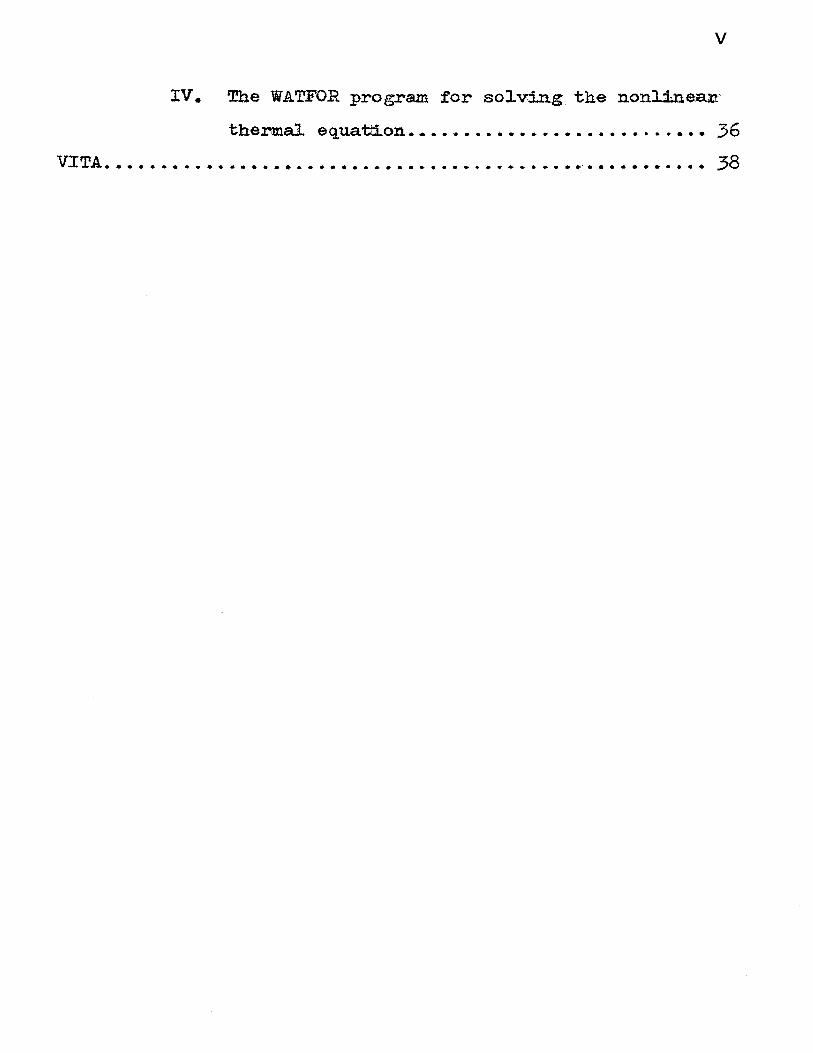
2. D-C cino.ui t and V ce vs Ic for d-e crl..raui t.... . . . . . . . . . 5
3. BJ.o«k diagram of thermal feedback •••.. . .•.•••••••••••• 9
4. Normalized juna:tion tempenat.ure vs power dissipation
* o:u.rve. with K as a . parameter. • • • • . • • • • • • • • • • • • • • • • • • • • 13
5.. Normal..:i.z.ed maximum power dissipation at thar.mal.
runaway vs.· normalized junctti.on tempera:tlura............. 14
6~ Common emittan· DC bias cirauitt ••••.••••••••••••••••••• 17
7. Cut-of:.fi' a:oJ.l.aa:b:or current: measuring eincmiti~... . . • . . . • 17
8. Comparison of experi.men tal. and theonetia:al cu~ves for
( e p c ) Max VS AT. • . • • • • • • • • • • • • • • • • • • • • • • • • • • • • • • • • • • • • • 22
9. Common emitter c:i..neui.t . for measuring hFE•••••········· 25 ~T/50 A-1 Comparison of equa~on hFE2 = hFE1 • . 2 and
exper:i..mental. resu1ts •••••••••••••••••••••••••••••••••• 35

.. VII
LIST OF nBLES
Pag~ 2-1 Experi.mental. Resul.ts for T"ransia.~r.:s:: 2N2142, 2N2143
.2N2144, 2}1'2145 ••••••••••••••••••••••••••••••••••••• 20
2-2 Expemmen.tal. Resul. ta:. for Transi.s.tors 2N1359, 2N1360
.2N"1529 t ,2N'1530. • • • • • • • • • • • • • • • • • • • • • • • • • .. • • • • • • • • • • 21
A-1 Daii:a and Resu1ts by usi.ng the Assnmpt:ton hFE2 = hn1 • 21>T/50 f!Or Tran&iators 2N2142, 2N2143, 2N2144
2N2145. • • • • • • • • • • • • • • • • • • • • • • • • • • • • • • • • • .. • • • • • • • • • • 32
A-2 Data. and Ra:sul.ts by usi.ng the Assumpt:Lon hFE2 =
hFEt• 2AT/50 for Tnans:istors 2N1359, 2Nl360, 2N1529
2N"1.530-. • • • • • • • • • • • • • • • • • • • • • • • • • • .. • • • • • • • • • • • • • • • • • 33
A-3 bper:tm.ental. darta of Short Circuit Current Gain hFE
by using ~s:Lstor 2N214,5 ••••••••••••••••••••••••• 34

T J
I co v eb
s
AT
Pc
eth
a
Ecc EBB
w
A
K
k
* k
* AT
e
* K
TA
Ic
IE
IB
Tth
1 CA
Re
• • •
• • •
• • •
• • •
. . . •••
. . .
. . . •••
.....
.....
..... • • •
• • •
•••
. . . •••
• • •
• • •
•••
•••
. . . • • •
• • •
LIST OF SYMBOLS
transistor junction temperature
leBO cut-off collector current
voltage drop between emitter and base
stabi:Lity factor
increment of temperature
col:Lector power dissipation
viii
total. thermal resistance from transistor ·case to
ambient
ratio of the collector current to emitter current
collector DC bias
base:~ Dc bias
par.a.meter
parameter
temperature co.ef'ficient of Ico
temperature coefficient of Veb
normalized collector power dissipation
normalized junction temperature
constant
normalized temperature coefficient of leBO
ambient temperature
collector current
emitter current
base current
thermal loop gain
collector current at operating point
emitter resistance

ix
~ • • • load r¢sistance
Rb • • • base resistance
RT • • • the total resistance of emitter and collector circuit
* PC • • • normalized collector power dissipation
(Ecc)th••• colle«tor power supply at thermal runaway
hFE ••• short circuit current gain
eJ-c··· thermal resistance from the junction to transistor
case
ec-s··· thermal resistance from the transistor case to heat
sink
Ss-A••• thermal resistance from the heat sink to ambient
rbb'··· the ohmic resistano:e between the aative base region,
B', of the transistor and the external base lead, B.
a •
0' •
9 •
• •
• •
• •
partial differential. operator
di:f:ference operator
thermal resistance
P dis a. • • a.ollector power dissipa ttl on

CHAPTER I
IN~DUCTION .AND REVIEW OF THE LITERATURE
A. Thenmal Requirements for Circuit Design
In the desigp of' a t:oansiator _ampl:i.fti..er cine:uit, the.r:&.:
are. two thermal. requirements wh:i.ah must be met :for satis
factory trans:Lstor openati.on.
1
1) The: g;neatest instantaneous heat:. released at the junctt:Lon
must flow through the ther.mu :i.mpedano:e at the lrlghest ..
ambient temperature ever encounte.ned without raising_ the
junction above its ma.x:lmum rate.d temperature. In other words:
2) The <rl.r.:aui t must be stabilized against thermal. runaway.
For requirement 1, if the junction temperature is hi~her
than :i. ts maximum .rated temperature, then the. trans is tor will.
be burned up.
For requirement 2, the power dissipation at tha:· coll.e.a±:or
junction :increases the junction temperature. TJ and henc:.e.
causes shifts in both Ico and V eb , there::fore some of the:
transistor parameters woul.d also be changed.
These sh:I...f:ts of operating point Q and transistor_
para.m.ete::rs rill cause some error :I..n transistor amplifier
cira:u.i t calcul.ations if we. assumed the. ool.l.ector junction
remaineQat the ambient temperature.
The shi:fLts in TJ and in the.: Q-point are" dependent upon
arc the va:J..ue: of stability factor S ( - a Ico ) ; i.:f' it is smaJ..l
then the shifts wil.l. be small and we do not need to take

2
care:· of the increases of juno.tion temperature. But if S is
large, then the circuit may be in an unstable condition for
which AT ( = T J - TA ) will be large and thermal runaway
may occur.
B. Defin:it:Lon of Thermal. Runaway
Thermal. runaway may be expl.a.:ined as a cha.l.n of events
rel.ated to the transistor jun~tion temperature, cut-off
col.l.ec:tor current:, and collector current. There:fere a rise
in junc;t,ti.on temperature al. ter.s the transistor. parameters :i.n
a direction that will increase cut-off coll.ea::tor current:
leBO • This incneased cut-off collector current:, in tu:on
increases the collector current, this increased collector
current may increase collector :power d:Lss:L:pat:Lon and
juno:t:Lon temperature. Th:Ls cycle repeats until f:inal.l.y the
transistor junction temperature reaches a point at wh:Lch
the collector current goes up infinitely.
We may conclude that thermal. runaway consists of a
repetition of the following thDee physi4a1 process:
1 ) A change in Ic results :in a change in P diss •
2) A change in Pdiss results in a change in TJ •
3) A change :1.n TJ results :ln a change in Ic •
These~ statements can be further :Lllustra~ed by the block
diagram of F1g. 1. where it is noted that:
· ·i' T J = 'th • 3 P c
~I . . ~I 00. w' co=aT
J
ei c

3
----p
f>Pc 9th alJ
~a ' ~leo _'Ole b ,.J
·-
'
~lc 6 - ~Ico
Figure 1 .. ·~ ~ IJ.J.ustrating positive .. · feedback associated with
thermal. runaway.

4
Hene:e. the moduJ.us of the thermal l.oop gain 'l'th o:f the:
system :is deduced from Fi.g. 1 • to ba.
• ep c ~I c
If Tth is equal. to or greater than unity then the, system
becomes unstabl.e, i..e. , the transi.ator circuit is under
the thermal runaway condition.
C. Discuss:i.Gn of Thermal Eguati.on in General. DC Bias
C:ir:r:uit
* From the mathematical derivati.on for a typi.cal
transistor DC bi.as circuit, we may finally obtain the
temperature change to be
(if AT is small.)
I:tr V is negative, then AT will. always decr.ease; if V i.s
positive and S is too 1arge, then ~T may become infinite
and thermal. runaway w:i.J.J. occur.
There.f'ore by the restriction on V :for stability, it i.s
ev:Ldent that for V:li>O, i.e. , ( Ecc - 2 IcA~ ) >o
E CC ........ -~ I
~ CA.. 2RT .
then
* ~:fer to Appendix I
5
'{e
I c..

Refer to F:lg. 2. This inequality shows that an
operating point q at Vcn£_ greater than one-ha1f the auppJ.y
voltage; Ecc wiJ.J. . give;: a '. :Large tempenatture. inareasa and
6
more bias sh:i.f'ts than. we may expect by cal.cu:Lating ~T as just
P9, and thenmaJ. runaway may oca:ur at that .. :point. In other
words.~ for stab:Le operation, the operating point indicated in
Fig. 2. should be be:Low the ~d-point m, i.e. Vee at
operating point has to be. smaJ..:Ler than one-hal. f the supp:Ly
voltage.

7
CHAPTER II
THERMAL RUNAWAY IN CLASS A OPERATION
In general., the:rma.J. runaway is not of importance exce.:pt
in class A amp~ifier operation, for example, :in transformer
coupled power output stages, where the load and emitter
resistance are negligibly small and almost the entire supply
voltage is across the transistor. If the input o.ira.uit is
also transformer coupled, then by the:: equation for stability
factor
* s = , therefore S = 1 and the ~ncuit
is possible ill a stable condition.
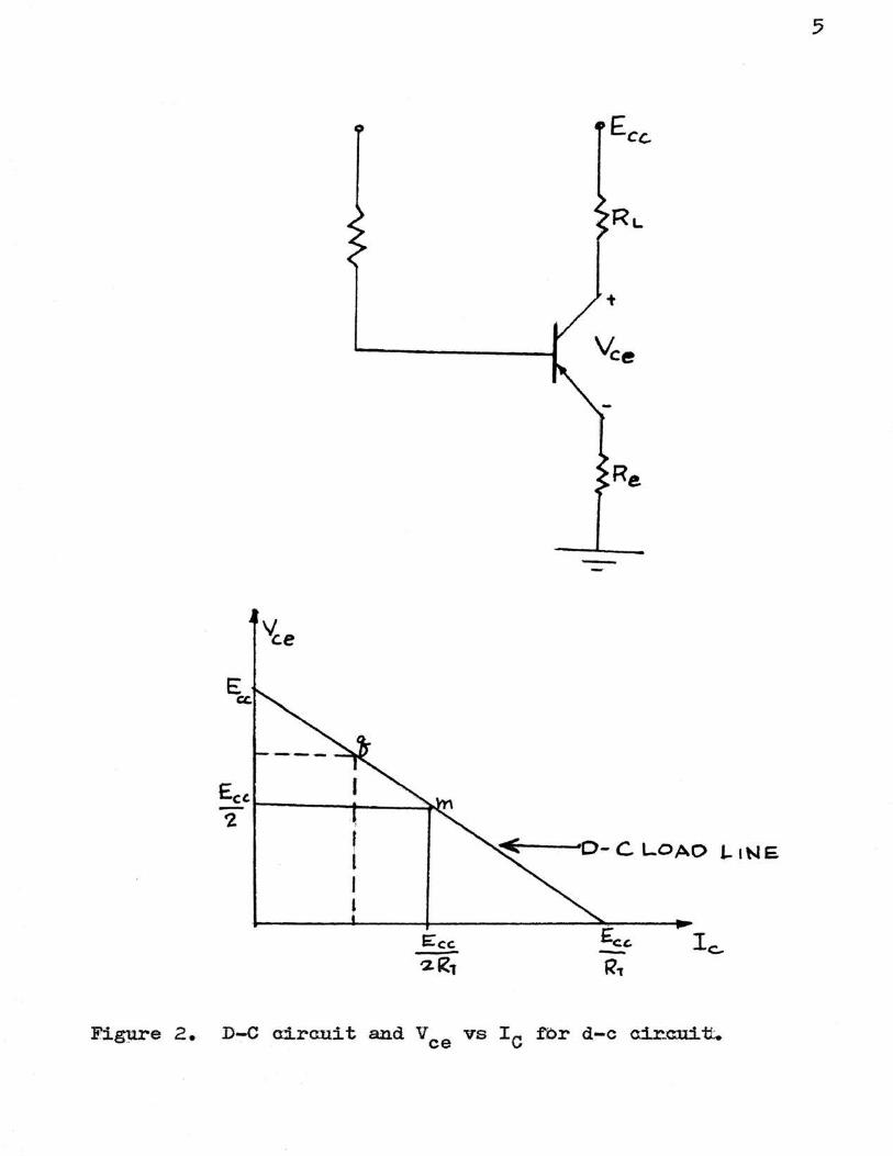
For convenience, we may construct a thenmaa cirauit as
shown in Fig. 3.
Various definitions and assumptions concerning the
circuit ar.e as follows:
1) The system operates under class A, no input signal
conditions.
2) The voltage drops across R_r. and Re ar..e negl.igi ble
compared with the supply voltage, so that Vee = Ecc •
3) Ic' is the collector aurrent with no Ico flowing, i.e. ,
at T = TA •
4) PC 1 = Ecc Ic 1 is the collector powar with no Ico
flowing.
5) e is overa:l.l. thermal. resistance from juncrtti.on to
* :Refer to Appendix I

8
ambient.
6) Fe - Eccic is the. total co11ector powe:rt;.
7) AT - TJ - TA = 6Pc is the difference, between the
ac::bual juna:ti.on temperature and ambient temperatune.
8) AV .b ... - k 4T where k = - 2.5 mv /°C e . AT
9) IC02 - IC01 • exp ( ) where., K is a constant
that governs the rate of increase of Ico with temperature.
10) Therma1 capacitances are ignored.
11) Ic01 is the I 00 at the ambient tempeDature, that is
when 4T = o.
12) w = Ecc • I 001 • s
a • E • S • k 13) A - CC .
lie+~
9
I~ ", Pc. J e AT
. i= --
AVeb - -~ -
Figure J. Block diagram of: thermaJ. feedback.

Now from the thanmai cirau2t
AT - ( e PC' ) + ( A a ) AT + e W exp ( A T/ K )
S.ol.ve. for AT to obtain
P c 'e + e W e:xp ( AT/ K ) .6-T:::~-----------
1 - A.e
TO
(1)
If'! we: assume that. a bias compensation, sua:h as diode
compensation, has been employed to remove the e£fect of tha..
variation :in the.. em:itterc-base junction voltage with
temperature, then A = 0 and
A T = 6 Pc ' + 6 W exp: ( b. T/ K ) (1-a)
By max:l.mizing PC 'e w:l th respecr,t to 6..T, wa obtain the
peak vcdue of .dT and 6Pc' •
( Pc' 8 )Peak = ATPe:ak - K (2)
B)' picking a · different vaJ..ue of K, and using WfJ as: a:
parameter we couJ.d generate a family of ( Pc' 9 ) vs 6.T ourves
and Equation (2) serves as a locus of points at which thermal
runaway occurs.
For simplicity, we may normalize equation (1-a) with
res-;pec t to we to 0 bta:in
eP • c we
AT
we - exp ( AT/ ew K/8W
* * * * P c = AT - exp ( AT I K )
The slope of all cur.ves is
* 1
)
d Pc
* dAT * * = 1 - --,. exp ( f:t. T I K )
K
* At A T - 0 •
(3)

11
* 1 d Pc
* =1--"'='*- sJ.o pe ini tia1J.y of a.-11 curves d AT K
* At A T = 0 fOr Equation (3)
* Pc = -1
* Maximum Pc occurs when 1 - ---4 -K
1 * * exp ( D.T I K )
* * * or K - exp ( AT I K )
* * * Thus A T = K ln ( K ) (4)
Substituting (4) into Eq~ation (3)
* * * then ( PC ) Max = ( A .T ) - K
which
when
Then
From
or
* * is zerto at AT = K
* AT = o. * ) * ( Pc - - K Max
* Equation (3) when Pc
* AT
AT
we
* * ) - exp. ( AT I K
* * = exp ( AT I K )
*
= 0
(.5)
At. the condition of Pc = 0 , when thermal runaway oconrs from
Equat:i.on (.5)
therefi:>re:
AT
we - e
and we= AT e
then AT= K
From the cli.saussd.on above two boundany c.ondi tions :for
sa::£6 opera:tion were obtained. As in Fig. 4, fOr a . given K,
the stia.bl.e operaXd.on region is batween these two J.ines and
each value of parameter we o:orres:ponds to a new AT.
Bllrthermore, rewr~te Equation (3) and Equat~on (4)
together
* * exp ( Ll ~ I K )
12
* * * AT = K ln (K ) (5)
~ay are two depend en t-var~abl.e simul tan eo us equa t:ions
* with K as a parameter. Theoret~cal.l.y it ~s possible to
* e1iminate K between them but because of the nonl~nearity
of the equations, we can not do l:Je.tter than ushg the
* * numer:tcal. method to draw a curve of ( Pc )Max vs AT as
shown in F1g. 5. from which we can see the re1ationship
* * between ( Pc )Max. and ( AT )Max •
:ElY" using this curve one may :predict the junct~on
temper~ture at thermal runaway when col.1ector power
dissipation is given for any k:i.nd of transistor.
If the bias compensation scheme is omitted, so that
A 1: 0, then we have the A 9 term :i.n Equation ( 1 ) • I .
~us P 8 ::: ( 1 - A 8 ) AT - We exp ( AT/ K ) c which can be written as
LlT 9P c' /( 1 - A e ) WB/(1- A9) we /(1
- exp ( L:,. T/ K ) Ae)
when normalized, this becomes .ft,
Pc ·v' * * * * = Pc = 4 T - e""Y"n ( AT I K ) W lf -·r
* K where K = VI&/( 1- Aft)
Using the same procedure as before, we f'ina1.1y coul.d

13
obtain the curves as shown :tn Fig. 4. and Fig. 5.
respectively.
z 0 -r<( a. ({) Ul -Q
(( lJJ
~ D Ul N
NORMAL\ZED JUNCTION TEMPERATURE
Figure 4. Normal.ized junction ,temperature vs powen dissipation
* aurve.: with K aa,: a pa::rame:tea:ot.

* (~ J MAX
?o
z C> t=-
40 & ~ ~
~
30 w i: &. ct 0
'20 ~ ...! ...1
3 :;: ::J ~
tO '>< <(
~
NORMALIZED JUNCTION TEMPERATURE INCREMENT_
Figure 5. Normalized maximum power dissipation at thermal
runaway vs normal.ized juna..tion te:mperature:.
14

t.5
C.RAP'fER III
EXPERIMENTAL
A. Objectives
~e objectives of the experimental measur•ments are to
oli:tain the transistor juna..tion temperatures at the thermal.
runaway points for several. dif'feren t power transistors in
tthe same common-emitter DC bi.as c:irctd t, and to compare
them. with the theoretical. val.ues gi-v:en in F.i..g. 5.
B. Design of). the Circuit
Because of the intention to induce thermal nun~way, it
is necessa.zzy- to build up .;m unstabl.e circui. t, which means to
make the _stability factor a.a. ~arge as possi.bl.e. For making
.S _l.arge, we may operate the transistor circuit as a cl.ass A \
ampl.ifier with high input resistano..-e. Furthermore, s:Lnc.e
the maxi naum power :is dissipated in the transistor wi. th no
signa1 present, we onl.y need to examine thermal. runaway in
the DC aircui t.
When the transistor is operating, col.l.ector dissipation
pow~r increases, which in turn :increases the june:tion
temperature, which caus~s heat to be generated within the
semiconductor. In order to reduce the junction tempera:tune,
a heat sink is required to direct heat from the junat:i.on
into the ambient air. For the objectives of this experiment,
a . hea:tt s:i.nk. that i.s jus:t lis enougll to :induce thermal.
run~ is Used. Al.so,in order. to reduce:. the hip thenmaJ
:impedance Of an air gap present b·etween the ma·t:ing surf'a.<te
of r~he semiconductor case and the heat sink sur:ta:ee, a · type_

120 thermal joi.nt compound is used'.
c.. Equipment
1 ) 1 miaroammeter
16
a) 3 DC power supplies ( one range 0-40 V tbn base bias, 2
range:' 0-32 V ar& in series for coJ.l.ao±or bias ) •
3) 2 ammeters ( 0-1 amp. )
4) Oven
5) Transistor parameter tester
D. Material.
1) 1 thousand~ohm resistor
2) 2 one-ohm resistors
3) Powen· transistor types: 2N2142, 2N2143, 2N2144, 2N2145,
2N1359, 2N1360, 2Nl529, 2N1530.
4) 120 s~oon joint «ompound
5) Heat s:i.nks: NC621, NC403
E. Pro e edU..re:
1 ) Measuring ICBO
In onder to det1e:rmin6' the) tempenatura-, croe£fd.c:1.en t of
leBO fibr a ' specified transistor, several values of ICBO at
ctlf'ferent te.mper_atura ara required.
Set the transistor cincrui.t board as india.ated :i..n F:ig. 7
into the: oven, then start to incn:te:a:.se: the:.. temperatura
from the ambient. In orcltnr· to keep the tempenature of the.
oven constant f'orr a sufficiently long t:tme~. at ea:ah step,
one mua;t. keep rotating the knob forward and backwatrd.
After the::. sc:al.e: i.ndi.cated that the tempera.11ura of' the
oven ia' nearly constant, ren:ord the vaJ..ua: oft cur:n.ent

l7
:Figure 6. Common emitter DC bias cira.ui t.
figure 7. eut-of:ff collector current measuring a:i.nauit.

18
flowing through the miaroamme.ter. Repaat the same proo:edure
at several. different temperature.
2) Testing of tha transistor short-cirGUit aurrent gadn
By usJ.ng the , tr.ans3.s.tor :parameter tester; the short cira.ui t _
current gain :fo.n-· a speaif'ied transistor at ambient temperature
is o bta:i.ne-d.
3) Satting the bias
Connect a one-thousand ohm resistor in the base. ai.:neuit:
and appl.y a naverse bias EBB w.hiah has the val.ue only a J.i ttle
bit larger than vbe ' that has= baen g:iven by manufac::tiuren' s
datax. Then connect the i;wo-ohm resis-tors in hoth emitter and'
collactor cirauits.
4) Apply a DC power supply :in to the coll.e:c±o:n aircruit as
reverse bias. Reaord the o:ol.l.ao.tior cur:r_ent at that instant
and after five minutes, then increase Ecc to a new v.a.lue.
Repeart the same proo..adu.r.a at each step. When the thermal.
runaway poi.nt is approaa.hed, the: a:ol.leator curnent will. go up
graduaJ.l.y for a given bias, and at themLal. mmaway the
a:olleo:tor current is increased very rapidly. One should
watch the increment very care~J.y and shut down the
system be:-:fore the maxi mum aJ.l.owable coll.eetor aurren t
has been rea<:hed, otherwise:- the transistor will l:Ie burned
up.
5) Since the aoJ.l.ec.tor eurr.ent used in Equation ( 1) is
~he one with no I flowing,. in. other words, it is the . CBO
coll.eeXor current at T = TA , the eoll~or dUrrent
o.orrespond.i.ng td the collector DC bi.as which woul.d' i.ndua-.e_

tharmaJ. runaway has to be examined again. Wait.~ unti.l tiha
elements of' the. circuits ane comple.tel.y o:ool.ed cfown uo
ambient: t:emper.adinre.., then 1iuim. on the syst.em and' set the.:
19
* colle:o.t.or Mas, at ( Ecc ) th and: necro:rd1 the crol.len.tor a.urnen t :
at 'tfuat·; i.nstan t · ac cro.r.ctl.ng:l.y.
6) Using, eight power transis.tors and repeating tha same
pnocedune..- ei.gll.t times, eight thermal nuna.way points were
obtained.
7) Ca1cuJ.at.e the juno.t:i.on temperature: by using the v:al.ues of
P'8 = Ecc• Ic• tT, k, K, ICBO, hFE, in Equation (1).
The IBM 360-50 a:om:pu te.r was used to sol v.e this nonl.ine.ai!!·
eq'\lattLon.
'* ( Ecc ) 1ih nepresen ts the o.oll.eo::tior;. DC Oi.as voJ. tage a .t wbich
thermail. runaway ocaurs.

.. - .. .. . -
TYPE Ecc. I~ el Ic.so K hFe Pee 6T A1' f:RRoR VOLT" AMP OHM /{)A oc T== teoc ·c "G D/o WA1T
T=l8~ EXP~R THE OR.
ZN- 4' 0-?5 3·\ 4o \1·8 1? 4a.e b4·'3 bB.l b·'ib z t4'Z
ZN- '21 0·~4, fi·8 4? l8· 'l. 9'5 '35·4 49·~ ?4·\ ~·'50 ?143
2N- 'lB 0-'l.'jh ?·8 ~t6 PJ.? eo 4l·q 54·S ?~·4 a.oo Zl44
2.N- ?O 0. 28'l JJ·B 18 \b·? ~? 4'3·0 b?·4 b~· \ 4·b0 'Zl41j
REMARK 1) ASSUME: h¥E CPN'S1'~NT
2) THEO~E \\CAL. VALUES of AI At=l.E' oP.rTAlNE"O fROM
50lVlN~ 1HE 'EGL (?) fOR. A {:,.\V~~ ?.e8
TABLE 2-\ EXPE R \ MENAl-: RE~UL1''S FOR TAAN'Sl51'0RS Zt\\2l4'2, ZN2l43, 'ZN2l44, '.2M2. \4-7
~ •
t.U <l> Ol
~ ~ I'D
(\) 0

~
.. . . ~ -
Ec.c lc. · el lc.eo ~ hFe p(:.e AT AI fRRoR
TYPE VOLT AMP JJA t T=:.IBC7c WA\i oc., oc. OHM
1= IB°C EKPER Tl-te'OR
ZN-l ~r;~
30 0·\2 ?·4- 335 24·4 40 \~·4 'lb· \ ~1·?
ZN- Z4 O.'l2 · ?·4 ?I ll·~ t40 ze.~ ~1·7 AD·O 1360
ZN- 3Z 0·32 5·4 30 l 112~
\b·~ '?'j . '7?·? 11· 'j 17-1
'ZN- '2.3 0·3') .,.4 6\ \4.4 ~0 4?·6 rjl·~ bl·4 t s;;o
- .
TABLE Z-Z
E.XPER\MEN\AL RESUL"TS fOR \RANS\'5\0RS ZN\3'5~/
2N I ~bO, Z.N l ?2~, 'l.N l?'3o
o/o
5·'2
6·0
l·'Z
b·~'J : I
N -

22
40 EXPERIMENTAL-+ •
+---THEORE-TICAL.-
30
20
( 0 .
10 z..o 30 40
TRANSISTOR JUNCT\ON TEIV\Pe;RATLIRE
F~gure 8. Companison o:r experimental. and thaonetical curves
for ( 9 Pc )Max vs .6-T.

CHAPTER IV
DISCUSSION AND CONCLUSIONS
There~ are several. problems inherent in calculating the
junction tempenature.
23
The first is unavoidable when tbe devi.ces.are considered
over a wide range o :f input parameters. It involves the
necess:i ty o :f assuming that the transistor pa!t"ameters such as
a . or rbb, are. constant w:i. th tempe.I!B.ture and with the
operating point. For exampJ.e, when thermal. runaway is
approached, Ic increases which norm.al.J.y decnease.s.; a; on the.
other hand, the temperature increases wh:Lch normal.~y increases
a. Ifno emitte-r resistance~ or a ver-:y small. emitter resistance
is employed, the stabil.ity factor S is equal to ( 1 + hFE ) ,
so that smal.J. changes in a wil~ hav..e J.acge: effects upon the:
runaway paint.
In this~ expeniment it is impossibl.e to obtain the exact
value of hFE and hence a at each bias step; o:f course one may
use the fundamental. current identity :for common emitter
transistor cirauit.: to sol.ve for a,
i.e. ,
liy using this equation, the author has met: the :following
difficul. ty.
1) Since the val.ue of a is very nearl.y equal to 1, and
also I co is a very small value, thus I 0 and IE may be verzy
cl.ose. Therefore i.t is hard to obtain the exact difference
between IE and Ic just by using a common current meter or a
oscilloscope. If they are not the exac'b~. vaJ.ue, then large

error wil.l. be induced.
2) S:i.nce the coefficient K is variable at each
tampe~ature for a given transistor, the ~ut off current
1000 obtained from the equation Icoz = Icol exp (A 'f/ K )
is unrel.iabJ.e. Thus it is evident that the val.ue of hFE is
di.fficul.t to estnate exactly from the. discussion above.
The onl.y wa:y to handJ.e this pro b~em seems to involve some
assumptions on hFE •
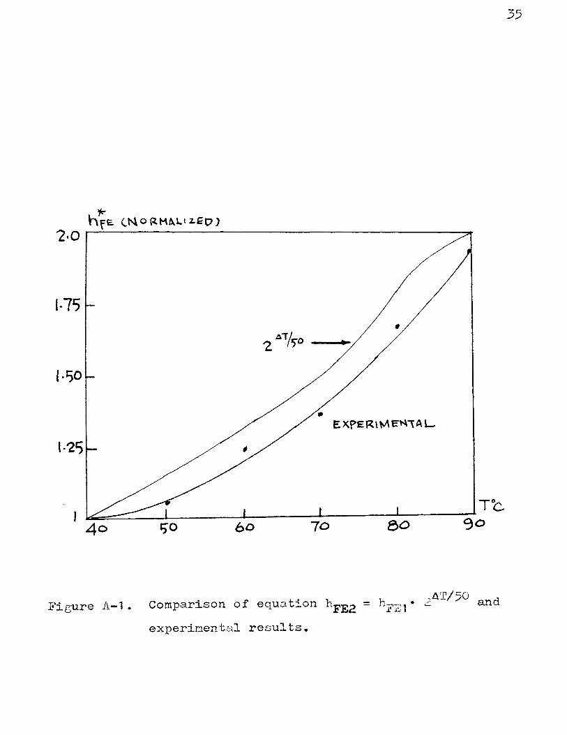
The first assumpt.:i.on made on hFE is by assuming tha:t
( AT/.50) . . ( hFE )T=1'A • 2 · and negl.ectJ.ng the i.nfl.uen.c.e
of Ic • This assumption is based on the investigation that 0
the short'.,..current gain will. be doubled for each 50 C
:increase for a germanium. semiconductor, in general.
In order to check the accuracy of this assumption, one
transistor was selected arbitrarily and used in the common
emitter DC circuit shown in F1g. (9).
Having properl.y biased the circuit, put the transistor
circuit board into the oven and heat it up from 20°C to 7o·c. 0
Record the values of Ic and IB for each 10 c increment.
~en appl.ying them into the equa.t:i.on
Ic
IB * the current gains at each tempema.ture l.evel were obtained.
By compari.sion with the a.ssumpt:i.on made on tba.· hFE
variation with temperature, a ; standard error o:f 11% was
* found •
* See Appendi.x II

25
R~..= t .n
~.:. \ ..n.
F:i.gure 9. Common emitter cincu:i t : for measuring hFE •
Upon us~g this assumption, for mjnjmum error, the
average::. vall.ue of K was used for ca.l.cul.at1.ng the juna.tion
26
' * temperatu:n.e, quite satisfactory results hav..e. b.a.en obtained •
But because the influence of collector current on the
variation of hFE coul.d not be neglected, the only reasonable
approach appears to be to assume the fall-off in hFE from
increased currant density will compensate for the increase
due to increased temperature. In other words, hFE is assumed
to be unchanged during the whole operating process --- ~his
is the sea:ond assumption made on hFE • A:flte:r aarefully
exam:i.ning thia; problem, it seems that the second assumption
is more reasonabLe.
Also for i.nducing the minimum error, tha :m:i.nimum. value ..
of' K was used instead' of average K. The r:esul t by using this
assumption is given on pages 20, and 21.
The second problem is the one of determining what val.ues
to use for e T , k, K.
The semiconductor manufacturer normally gives the
thermal resistance from the junction to the: transistor case
i J -c • 'f'.he hea.;t sink manufacturer gives the thermal.
resistan<;.E3: from the heat sink to ambient 9 S-A • The only
thing remaining to exam; n e is the thermal resistance from
transistor case to heat sink e c-s • Because of the
dependence of the flatness: of the heat sink surfan.a: and
semiconductor surface:, when using 120 joint compound for a
* .S.ee Appendix II

given semiconductor aase atyle, it is unexpected to
estimat:e an exact va1ue of. 6 C-S •
An av.erag~ va1ue o.f' a c-s :fOr different de:gr.ees ofi
f'~atness was: se1eo:ted :i.n this exper:i..m.ent. Of: cou.nse:, some
smaJ.l ernor was induc:ed.
27
AE£ neg.ard to k, for simplici. ty no a.tttempt. was'. made. to
meast~..r.e k. Itt is dea:i.nable to ass.ume k to ba: -2.5 mv/o C fbl:!
each transiaton. ~e nea.son f'o:n · usi.ng_ this assumption :is:
that. k rll.l not infil.uenoe the juna.t:Lon tempenat~e
appzre!;iably in this experiment.
Be.cauae of' the di.f'fd.cul ty of'. keeping the tampel.1a.t.ur.e
o:f. the: oven constant when maasuning Icoo , di.f:fi~ent:. va.:Lues
of K wene introduced for each measunment:. Joyce & Clark ( 1)
sugg_estt 'tihat one shoul.d assume the lowes:tt expected v:al.ua
fon K. By using thia suggestion and asm1ming hFE o:onstant
dur:tng the w.ho1e process, a set of tabul.at:e.d data and
diagrams we:o:e obtained as shown on page 20, 21, and 22 •
.All :1n a11, these:. considerations add up to make a
a.e:rta:in amount o:e: guesswork. ~erefore., the error ll.e .tween
the exper:imental. and· theoretia:aJ.. results for ea<Ih tnansisto:rr
is: in the range: of. 5-1 0 %.

BIBLIOGRAPHY
1. Joyce, M. V. , and K. K. Clarke~ (1961) Transistor
Cirau2t Analysis. Addison-Wesley, Massachusetts, p. 66-
144 •
28
2. Texas Instruments Incorporated, Transistor Ciraui.t Desi.gn.
McGraw-Hill, p. 55-58, p. 105-123.
3. Pierce J .F. Transistor Circuit Theory and Design. Charles_
E. Merrill~ Ohio, p. 177-208.
4• John, E.A.J. , and J. J. Hilliard, Heat-Sinking Techniques
for Power Transistor in A Space Environment. IEEE
Transactions on Space Electronics and~ Telemetry, June.
1963.
5. Goldman, W. E. The Art of Heat Sinking, Wakefield
Engineering, Massachusetts.
6. Mortenson, K. E. , !t'rans:i.a,tor Junction T~mper.a t:w:re. as A
Function of Time. Proceedings of The. IRE April, 1957,
p. 511-512.

APPENDIX I
DERIVATION OF THERMAL EQUATION
For the input c:i.rau.i. t
E = ReiE + veb + ((1-a) IE - Ico ) ~
- (Re + (1-a) ~ ) IE + veb - leo~
Therefore
E - vebl 1co1 Rb Let 1El - +
R + (1-a) Rb R + (1-a) ~ e e
E - veb2 I C02 ~ IE2 - +
R + (1-a) ~ R+ (1-a) ~ e e
therefore
29
< r)
(2)

where AV eb = Veb2 - V eb1
From ( 1) we obtain the variation eq~ation for 6. Ic
Aic = aAIE + AICO
.Substitute AIE into (3)
Arc -a aveb
-R + e (1-a)
-aAVeb =
R+ e
By definition
arc .s ' -= ----- -
therefore
( 1-a)
Let:: Ic = ICA + Aic
l:J.Vb=-k6T e
Rb
~
+ a .6.Ico ~
R+ e (1-a) ~
+ (Re +Rb) Aico
R + e ( 1-a) Rb
AT/K .6 ICO = ICOA ( e - 1 )
Re + ~ = ~
+ ~Ico
30
(3)

31
Then P0 ~ Ecc • r0 - Ic2 ( ~+ R8 )
= (ICA + 6.Ic) {ECC - (ICA. + 6 Ic) RT)
- (IC.A.ECC - l.CA 2 ~) + Aic( Ecc- 2 1cART- AIC~ )
2 Now PA = IcAECC - ICA RT
and in g~eral 2 leA>> A Ic 1n any <rl.reui. t for good stabi.li ty,
so that the A Ic 2 ~ term may be..' droppe:d.
theret'ore..
· for S ~ 1 then 6 'r wil.l. be. smal.1
AT Iff <.. 0.3
AT then e AT/K - ! = --
K
(4)
Making this substi.tut:i.on i.nto Equati.on (4) giv.ea tha thennal.
eq]:lation

-- · -
Ecc lc 9r lcso y, hFE Ra 6T · bT ERROR TYPE' L :. ·. - 1
VOLT AMP OHM )JP,. -'C 1= \f>£:, wAlT oc, ! oc /o 1= 1eoc ~XpER · TH:foR
1
:.lN· · 4-S 0·3? 3· \ 4-0 23 75 48·6 ~~-l . bB·~ ~·7 'Z\4l
... . .
ZN- 1.1 0· 2.4~ . ~·8 4~ '?.5·1 ~? 38·4 48·8 '54·' ~·~ Zl45 ... ~ . ..
ZN- Z8 o.Z')'=' r; ·8 26 Zl44
'ZO eo 4\·~ ?4·~ '5'~·4- 8·0
' -
ZN- 30 o.'ZSZ ?·B \e> Zf4?
'22· ~ ~5 4~ '=>t;·+ 6g·l 4·b
TABLE A-1 ~TA AND RE5UL.'T5 BY U~\NC( iHE A~SUMPi\ON hF£'1=hfli' · 2'lT/~o
fOP. 1RAN~t5TOR5 ZNZ142, 2N2l4~, ZN Zl44, 2NZJ47
~ s tzj
~ ~ H
ttl
~ ~ 1-3 t-3 ~ H 0 z t;j
:r:-t-3
nf >
R1 ~ t1
II
~ .f tzj t:1 ~
• ~ "i>~ ~ ~ ~
~ ~
~ 'tl
! H ~
H H
\.N (\)

--
TYFt Ecc. Ic eT I ceo r<- hFE rce AT AT ~RoR
VOLT AMP OHM -1)A "c T=lBt WA\T oc fc I ·c • 0 I
T== \5-c.. EXPE~ iHEOR
Z.N-135~
30 0·\ z 5·4 33~ 2B 4-0 1~·4 Z8·1 'Z7·3 r;.z
ZN- 74 o.zz ?·4 51 Z2.4 140 'ZB·? 37-(:, 40·0 6·0 \3b0
2.N- 3Z. 0·32. 5·4 30 2l·? 35 55'-3 '7-7 77·1 13·8 l5Z9
2N- '23 1530
0·3? ?·4 61 2b·5 90 43· 5 57·6 ,,.4 6·'3 '5
TABLE A-2 DATA AND RE.5ULT5 8'( USING THE A55UMPTtON hFe1=hf~' · ZA)T/~o
FOR 'TRANSISTORS Z.N 13?~1 ZN l'3b0, 'ZN1?2.q, 2.N 1530
~

0 ' T c :
40
50
60
70 ··----
80
90
APPENDIX III
EXPERIMENTAL RESULTS OF CHECKING THE
ACCURACY OF EQUATION hFE2 = hFEl .. 2/lT/50
MA M.A. NORMALIZED t_T/50 Ib Ic;: hFE hFE DIFF.
.~- -···
0.?48 11.5 154 1 1 0
0.?45 121 162 1.05 1 .14 o.o9
0.730 139 191 1.25 1.32 0.0?
0.?30 153 210 t .36 1.49 0.13 ·- - -
0.?15 183 257 1.6? 1.82 0.15
o.690 207 299 1.94 2 0.06
TabJ.e A-3 Exper:tmentail data ofr shor..t cirmdt canrent
gain hFE 1ly using transl.stor 2N2145
Standard Error= j <0 ·022 2+Co.oz) 2+(0.122 2+(o.1!22 2+(o.o6) 2
5
34
=" o,0081 + o.oo49 + o.o169 + 0,0222 + o,0036 5
- 11 %
35
"F" hre. (.~ o RM~LI Z.ED) £.0~-----------------------------------
1-1?
I .r;o
EXPER\ME~1:AL
1·'2'5
')0 60
F . A 1 c . f t• h h ?~T/50 d •J..g;ure .<~.- • omparJ..son o equa J..On FE2 = FEl • ._ an
experinental results.
1 ~
2
3·· ~
5 6 7 8 9
10
11
12
13
14 15 16
1? 18 19 20
21
22
23
24 25 26
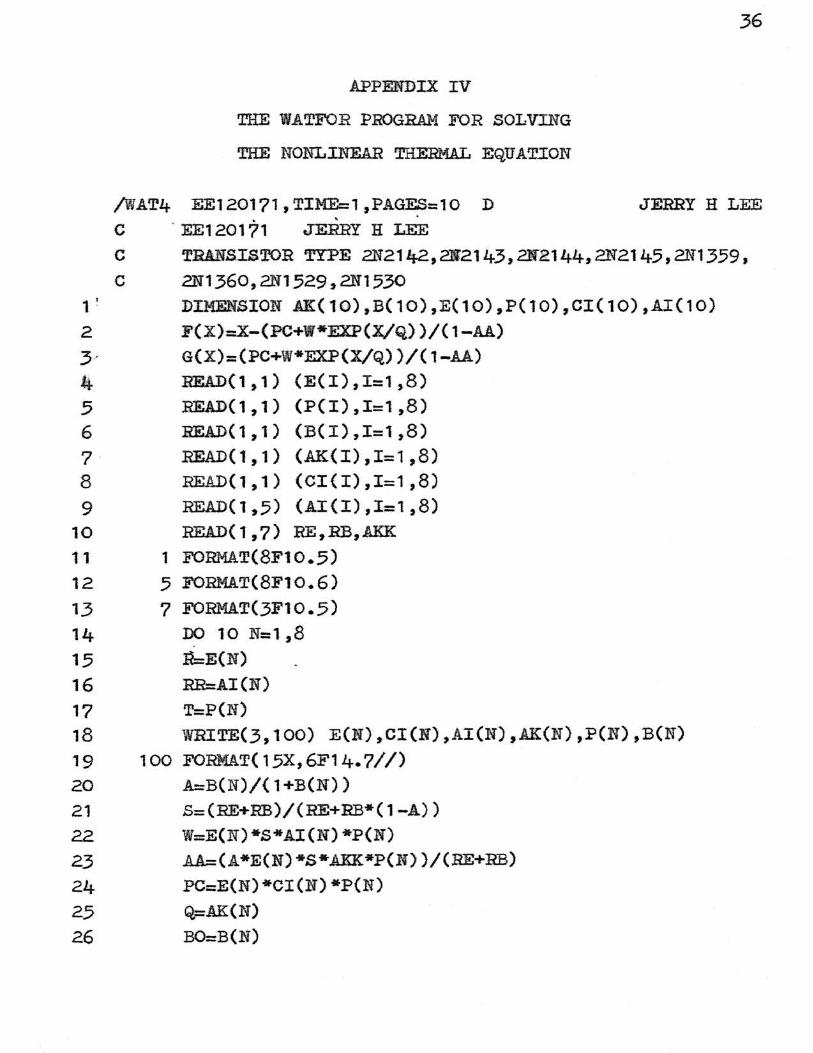
.APPENDIX IV
THE WATFOR PROGRAM FOR S-OLVING
THE NONLINEAR THERMAL EQUATION
36
/WAT4 EE1201?1,TIMEC1,PAGES=10 D JERRY H LEE c . EE1201'71 JEBRY H LEE
c c
TIUNSLSTOR TYPE 2N2142,211'2143,2NR144,2N2145,2N1359,
2N1360,2N1529,2N1530 DIMENSION AK( 1 0) ,B( 10) ,E( 10) ,P( 1 0) ,CI( 1 0) ,AI( 1 0)
F(X)::X-(PC+W*EXP(X/Q))/(1-AA) G(X):(PC+W*EXP(X/Q))/(1-AA) READ(1,1) (E(I),I=1,8) READ(1,1) (P{l),I=1,8) READ(l,l) (B(I),I=1,8) READ(1,1) (AK(I),I=1,8) ~JD(l,l) (CI(I),I=1,8) READ( 1 ,5) (AI (I), I=l ,8) READ(l ,7) RE,RB,.AKK
1 FORMAT(8F10.5) 5 FORMAT(8F10.6) ? FORMAT{3F10.5)
DO 10 N=1,8 IbE(N)
RR::.A.I(N)
T P(N) WEaTE{3,100) E(X),CI(N),AI(N),AK(N),P(N),B(N)
100 FORMAT(15X,6F14.7//) A=B(N)/( 1 +B(N))
S=(RE+RB)/(RE+RB*(1-A)) W::E(N) *S*AI(N) *P(N) AA=(A*E(N)*S*AKK*P(N))/(RE+RB) PC=E(N)*CI{N)*P(N) Q=AK(N)
BO=B(N)
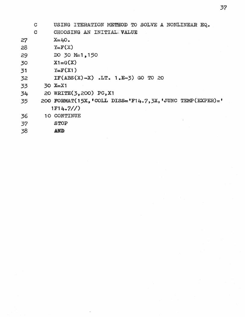
c c
27 28 29 30 31 32 33 34 35
36 37 38
USING ITERATION METHOD TO SOLVE A NONLINEAR EQ.
CHOOSING AN INITI.AL:;- VALUE
X::40.
Y=F(X) DO 30 M;: 1 , 1 50 X1=G(X) Y=F(X1) IF(ABS(X)-X) .LT. l.E-3) GO TO 20
30 X=Xl
20 WRITE(3,200) PC~X1
37
200 FORHA'f( 1,5X, 1 COLL DIS.Sc 'F14. 7 ~ 3X~ 'JUNC TEMP(EXPER)= 1
1F1It.7//) 10 CONTINUE
STOP .AfiD

VITA
The author was born on Octobe;n_ 2, 1943, :in Kan-su,
Ch:lna. He received his: primary and high sahool e .duo.ar.tion
in Taipei, Taawan, China. He rece:i ved' hia a.ollege educ.ation
:in National. Taiwan Uni ver.si ty, Taiwan, China, and a btained a
B.S. degree in El.ectrical. Engi.neer:ing in June 1965. Ha. came.
to the Unite.d Sta:bes in October 1:966 and enrolled in the
Graduate School of The Un:iv.e:nsn_ty of Mi.ssottri. at Rollai in
January, 1967.