Aberrant Ventricular Conduction Types and Concealed Conduction
Upload
nguyentrucCategory
view
219download
1
K. E. Goodson Mechanical Engineering Department,
Stanford University, Stanford, CA 94305-3030
Thermal Conduction in onhomogeneous. CVD eamond Layers =n
Electronic Microstructures Chemical-vapor-deposited diamond layers of thickness between 0.1 and 5 ,am have the potential to improve conduction cooling in electronic microstructures. However, thermal conduction in these layers is strongly impeded by phonon scattering on defects', whose concentrations can be highly nonhomogeneous, and on layer bound- aries. By assuming that defects are concentrated near grain boundaries, this work relates the internal phonon scattering rate to the local characteristic grain dimension and to the dimensionless grain-boundary scattering strength, a parameter defined here that varies little within a given layer. Solutions to the Peierls-Boltzmann phonon transport equation for conduction along and normal to layers account Jbr the nonho- mogeneous internal scattering rate. Predictions for conduction along and normal to layers as thin as 0.2 ,am agree well with room-temperature data. This research helps optimize diamond layer thicknesses for specific microstructures, such as silicon-on- diamond (SOD) circuits.
1 Introduction
At room temperature, chemical-vapor-deposited (CVD) dia- mond can be both an excellent thermal conductor and an electri- cal insulator, making it ideal for passive use in electronic micro- structures. The benefit is greatest if diamond can be brought within micrometers of active regions, typically made of silicon or gallium arsenide (Goodson, 1995). The small separation allows the diamond to reduce the problem of local hotspots with micrometer-scale dimensions, which degrade the perfor- mance and reliability of electronic systems. One example is a high-power-density laser-diode array based on a novel compos- ite diamond/gallium-arsenide substrate (Goodson et al., 1995c). Another example is a. silicon-on-diamond (SOD) cir- cuit in which a thin diamond layer separates active silicon re- gions from the substrate (Ravi and Landstrass, 1989). SOD circuits are a novel form of silicon-on-insulator (SOI) technol- ogy, which improve the speed and voltage-blocking capability of devices through the use of a buried insulating layer. The use of diamond as the buried insulating layer offers the promise of avoiding the thermal resistance due to conventional buried insulators, such as silicon dioxide (Goodson et al., 1995a). Temperature fields in SOD circuits are strongly influenced by conduction along and normal to diamond layers thinner than 5 # m .
The deposition of thin diamond layers on silicon yields a highly imperfect and nonhomogeneous material, particularly near the interface. This is evident in the grain structure, which is shown in the cross-sectional micrograph in Fig. 1 and approx- imately depicted in Fig. 2. The nucleation of diamond on a silicon substrate results in very small grains near the interface (e.g., Stoner et al., 1992). The scattering rate of phonons, which are responsible for heat conduction in diamond, is strongly in- fluenced by the local grain size. However, the relationship be- tween the phonon scattering rate and the grain size has not
Contributed by the Heat Transfer Division and presented at the Fourth ASME/ JSME Thermal Engineering Joint Conference, Maui, Hawaii, March 19-24, 1995. Manuscript received by the Heat Transfer Division February 1995; revision re- ceived December 1995. Keywords: Conduction, Electronic Equipment. Associate Technical Editor: R. Viskanta.
been rigorously determined. In thin layers, heat conduction is influenced by the strong nonhomogeneity of the phonon scatter- ing rate, which results from the varying grain size, and by phonon scattering on the layer boundaries. Predictions require solutions to the phonon transport equation in nonhomogeneous layers, which are not available.
Previous data demonstrated the strong dependence of the local thermal conductivity along diamond layers on the coordinate z in Fig. 2 (Graebner et al., 1992a, b; K~iding et al., 1993, 1994). The room-temperature conductivity varies from approximately 2000 W m -~ K -~ for values of z greater than about 150 #m, to values below the conductivity of silicon, 150 W m -1 K i, for values of z less than about 5 ,am. Recent work measured the effective thermal conductivities normal to tNnner layers, obtaining values between 12 and 75 W m -t K -~ for layers of thickness 0.2 and 2.6 ,am, respectively (Goodson et al., 1995b). Previous analysis solved the transient equation of phonon radiative transfer for conduction normal to diamond layers using the homogeneous phonon-scatter- ing parameters of nearly perfect crystals (Joshi and Majumdar, 1993). There is a need to solve the transport equation considering the nonhomogeneous, highly imperfect conditions in contemporary layers of thickness less than a few micrometers.
This work develops a theory for the dependence of the local phonon scattering rate in diamond layers on the local characteristic dimension of grains, da. The phonon transport equation is integrated for the case of conduction along a layer with a nonhomogeneous phonon mean free path, yielding the effective thermal conductivity as a function of layer thick- ness, temperature, and parameters describing the grain struc- ture. An approximate solution to the transport equation for the case of conduction normal to a nonhomogeneous layer is also given. Predictions for conduction along and normal to diamond layers as thin as 0.2 ,am are compared with experi- mental data. This work is of interest to researchers fitting the temperature-dependent conductivity in diamond polycrystals, who lack a precise treatment of the scattering rate due to grain boundaries. This research helps quantify the benefit of using passive diamond layers in electronic microstructures, which is governed by the ability of the layers to conduct heat from active semiconducting regions.
Journal of Heat Transfer MAY 1996, Vol. 118 / 279
Copyright © 1996 by ASMEDownloaded 21 Nov 2008 to 171.64.49.29. Redistribution subject to ASME license or copyright; see http://www.asme.org/terms/Terms_Use.cfm
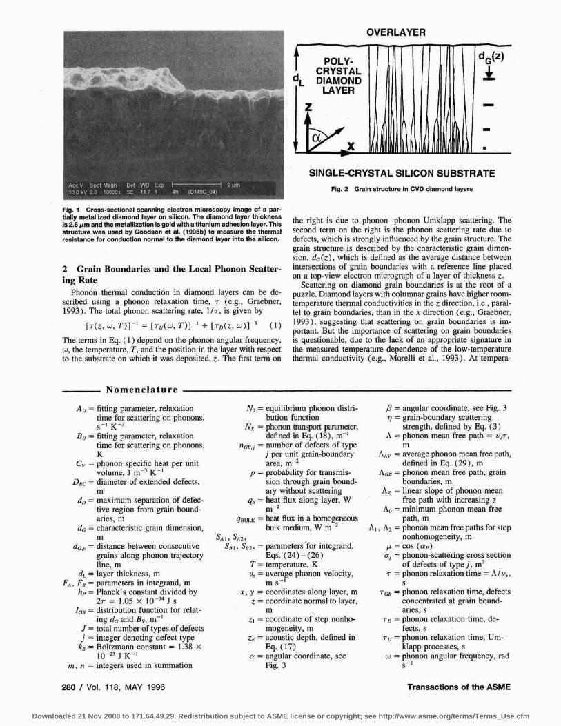
Fig. 1 Cross-sectional scanning electron microscopy image of a par- tially metallized diamond layer on silicon. The diamond layer thickness is 2,6/.¢m and the metallization is gold with a titanium adhesion layer. This structure was used by Goodson et ai. (1995b) to measure the thermal resistance for conduction normal to the diamond layer into the silicon.
2 Grain Boundaries and the Local Phonon Scatter- ing Rate
Phonon thermal conduction in diamond layers can be de- scribed using a phonon relaxation time, r (e.g., Graebner, 1993). The total phonon scattering rate, l / r , is given by
[v-(Z, w, T ) ] - ' = [7-u(W, T)] -1 "t" [TD(Z, W)] : ' (1)
The terms in Eq. ( 1 ) depend on the phonon angular frequency, w, the temperature, T, and the position in the layer with respect to the substrate on which it was deposited, z. The first term on
POLY- CRYSTAL DIAMOND
LAYER
OVERLAYER
=,,,
!l/Ill
m
dG(Z)
SINGLE-CRYSTAL SILICON SUBSTRATE Fig. 2 Grain structure in CVD diamond layers
the right is due to phonon-phonon Umklapp scattering. The second term on the right is the phonon scattering rate due to defects, which is strongly influenced by the grain structure. The grain structure is described by the characteristic grain dimen- sion, do(z), which is defined as the average distance between intersections of grain boundaries with a reference line placed on a top-view electron micrograph of a layer of thickness z.
Scattering on diamond grain boundaries is at the root of a puzzle. Diamond layers with columnar grains have higher room- temperature thermal conductivities in the z direction, i.e., paral- lel to grain boundaries, than in the x direction (e.g., Graebner, 1993), suggesting that scattering on grain boundaries is im- portant. But the importance of scattering on grain boundaries is questionable, due to the lack of an appropriate signature in the measured temperature dependence of the low-temperature thermal conductivity (e.g., Morelli et al., 1993). At tempera-
N o m e n c l a t u r e
Au = fitting parameter, relaxation time for scattering on phonons, S-1 K-3
Be = fitting parameter, relaxation time for scattering on phouons, K
Cv = phonon specific heat per unit volume, J m -3 K -I
DRc = diameter of extended defects, m
dD= maximum separation of defec- tive region from grain bound- aries, m
d~ = characteristic grain dimension, m
d~,. = distance between consecutive grains along phonon trajectory line, m
dL= layer thickness, m FA, Fe = parameters in integrand, m
hp = Planck's constant divided by 27r = 1.05 × 10⁻³⁴ J s
Ice = distribution function for relat- ing dG and By, m -1
J = total number of types of defects j = integer denoting defect type
ke = Boltzmann constant = 1.38 × 10 .23 J K - '
m, n = integers used in summation
No = equilibrium phonon distil- /3 = bution function ~7 =
Nx = phonon transport parameter, defined in Eq. (18), m -l A =
naBj = number of defects of type j per unit grain-boundary AAV = area, m -2
p = probability for transmis- A6n = sion through grain bound- ary without scattering Az =
q, = heat flux along layer, W m -2 Ao =
qBVLK = heat flux in a homogeneous bulk medium, W m -2 Al, A2 =
SA,, SA2, SBi, Sez, = parametersfor integrand, # =
Eqs, ( 2 4 ) - (26) a: = T = temperature, K v, = average phonon velocity, r =
m s - ' x, y = coordinates along layer, m roe =
z = coordinate normal to layer, m
zl = coordinate of step nonho- rD = mogeneity, m
ze = acoustic depth, defined in ru = Eq. (17)
c~ = angular coordinate, see ov = Fig. 3
angular coordinate, see Fig. 3 grain-boundary scattering strength, defined by Eql (3) phonon mean free path = u:- , m average phonon mean free path, defined in Eq. (29), m phonon mean free path, grain boundaries, m linear slope of phonon mean free path with increasing z minimum phonon mean free path, m phonon mean free paths for step nonhomogeneity, m cos (Otp) phonon-scattering cross section of defects of type j , m 2 phonon relaxation time = A/us, S phonon relaxation time, defects concentrated at grain bound- aries, s phonon relaxation time, de- fects, s phonon relaxation time, Um- klapp processes, s phonon angular frequency, rad S-1
280 / Vol. 118, MAY 1996 Transactions of the ASME
Downloaded 21 Nov 2008 to 171.64.49.29. Redistribution subject to ASME license or copyright; see http://www.asme.org/terms/Terms_Use.cfm

tures above a few degrees Kelvin, the rate of phonon scattering on distinct grain boundaries, which is independent of the phonon frequency, is much smaller than the rate of scattering on other types of defects, e.g., impurities, which depends strongly on the phonon frequency.
An explanation is suggested by the electron micrographs of Heatherington et al. (1990), which show a high concentration of defects within about 2000 A of grain boundaries. Scattering on defects concentrated at grain boundaries yields anisotropy in layers with columnar grains and has the phonon frequency dependence needed to explain low-temperature conductivity data. Goodson et al. (1994b) used this assumption to relate the effective thermal conductivity along layers to do, yielding predictions in reasonable agreement with data for which the local value of de is known. This work assumes that in layers of thickness less than a few micrometers, the small grain dimen- sion causes phonon scattering on defects near grain boundaries to dominate over scattering on defects within grains. This allows 1/TD in Eq. ( 1 ) to be replaced by 1/~-6B, which is the scattering rate due to grain boundaries. This work also assumes that I/7-D can be treated as homogeneous within a given plane z in solving the phonon transport equation, even though the scattering rate must be higher near grain boundaries. This yields accurate pre- dictions of the heat flux as long as (a) the characteristic length scale of the medium in which transport is analyzed is large compared to da and (b) the geometry is such that energy must travel through many grain boundaries, both of which are satis- fied here.
This analysis uses two different approximations to relate 1/ TO, to de. The first, approximation A, distributes the defects contributed by grain boundaries homogeneously within the plane z. The second, approximation B, assumes that the defects contributed by a grain boundary are located within a distinct distance from grain boundaries, do, that is finite but much smaller than de. For case B, the scattering rate due to grain boundaries is analyzed considering ballistic phonon transport between boundaries, at which phonons have a probability for transmission without scattering. For both cases, the total scatter- ing rate is calculated using Eq. (1) with the expression for the scattering rate due to grain boundaries derived in the following subsections. Approximation A is most appropriate for do ~ do and approximation B is most appropriate for dc >> do. The electron micrographs of Heatherington et al. (1990) indicate that dD ~ 2000 A for grains with dc ~ 1 #m. Since grain dimensions in diamond layers vary between a few tens of nanometers to several tens of micrometers depending on the coordinate z, both approximations are of practical impor- tance.
2.1 Approximation A: Lateral.Homogeneous Distribu- tion of Defects Related to Grain Boundaries. Because grain-boundary scattering is considered geometrically in this work, it is helpful to define a mean free path for scattering on grain boundaries A~, = ~-G,v,, where v, = 1.32 × 10⁴ m s -t is the average phonon velocity in diamond. Given approximation A, the inverse of the mean free path can be expanded using
[AeR(z, tv)] - l = Bv(z)~7(z, w) (2)
where By is the grain-boundary area per unit volume. The scat- tering rate determined using Eq. (2) can be applied directly in Eq. (1). The dimensionless grain-boundary scattering strength is defined here,
J
rl(Z, ~) = ~ aj(w)nGBj(Z) (3) j = l
where cr is the scattering cross section of defects of type j for phonons of frequency ~o. The concentration of defects of type j is the product of the number density of those defects per unit grain-boundary area, neB,j, and By. Section 2.2 shows that rl is
PHONON ~ 1 TRAJECTO~ ~ p I
VECTOR '~ NORMAL ~ I ~ TOAREA"~,~,,~L-G~ ~ |
GRAIN BOUNDARY AREA ELEMENT
x iiJ
y, Fig. 3 Angles describing a phonon trajectory and a differential grain- boundary area element
simply related to the probability for phonon transmission through a grain boundary without scattering.
This work derives the relationship between By and dG by assuming that do is independent of the direction of the reference line within a given x-y plane. This is not strictly correct for nearly heteroepitaxial layers, which have a large fraction of grain boundaries oriented in the crystallographic directions of the underlying silicon substrates (e.g., R6sler et al., 1993). But the oriented grains prevail only for relatively large values of z, so the present approach is still appropriate. The angles aGR and /3oR of the area-element normal vector and a set of relative rectangular coordinates are defined in Fig. 3. The grain-bound- ary area per unit volume is
uff/2 I~B(Z, ae,, /36.) d/3~Rdae, (4) By(z) = 4 sin (aeB) cos (/3~s)
where Io,(aG,, 13o,)daoBd/3aR is the number of intersections per unit length of grains of angles ac, B and fit8 with the x ' axis, which serves here as the reference line for the measurement of do. The denominator of the integrand in Eq. (4) accounts for the increased contribution of grain-boundary area per unit vol- ume by area elements with normal vectors not parallel to the reference line.
If the grain structure is random, then I~, is
l~B(z, ol.B, /~o~)
= [sin (aaB)][sin (~cB)lcos (Bcn)Jl 2~rd~.(z)
The first term in brackets accounts for the fraction of grain- boundary area elements in the x ' - y ' plane having angle acB, which decreases to zero with a~B. The second term in brackets accounts for the diminished profiles presented by grain-bound- ary area elements whose normal vectors are not parallel to the reference line. In layers with columnar grain structure, grain boundaries are predominantly parallel to the z axis but have intersections with x ' - y ' planes that are randomly oriented. For this case, IG, is
loB(Z, ~.I,, l~n)
= 6 o ~ 2 2
Journal of Heat Transfer MAY 1996, Vol. 118 / 281
Downloaded 21 Nov 2008 to 171.64.49.29. Redistribution subject to ASME license or copyright; see http://www.asme.org/terms/Terms_Use.cfm
! , 0
0.1 "%. 0.01 0.1 1 1 0
G R A I N - B O U N D A R Y S C A T T E R I N G S T R E N G T H , TI (m)
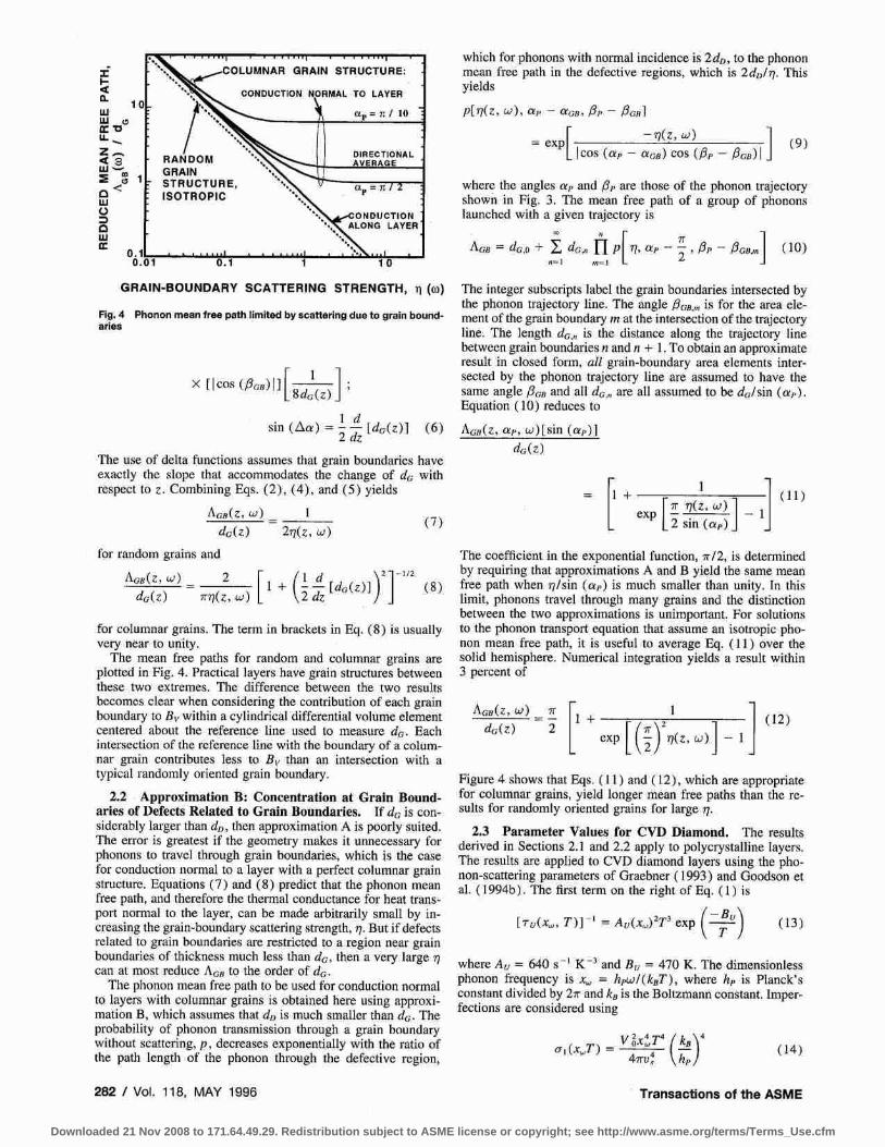
Fig. 4 Phonon mean free path limited by scattering due to grain bound- aries
X [Icos ( t o . ) [ ] [ 8dc---~---(z) 1 ",
1 d sin (Ac~) = ~ z z [do(z)] (6)
The use of delta functions assumes that grain boundaries have exactly the slope that accommodates the change of do with respect to z. Combining Eqs. (2), (4), and (5) yields
Ao.(z, co) _ 1 ( 7 )
do(z) 2r/(z, co)
for random grains and
Ace(z, co) _ 2 1 + [do(z)] (8) do(z) 7r~7(z, co)
for columnar grains. The term in brackets in Eq. (8) is usually very near to unity.
The mean free paths for random and columnar grains are plotted in Fig. 4. Practical layers have grain structures between these two extremes. The difference between the two results becomes clear when considering the contribution of each grain boundary to By within a cylindrical differential volume element centered about the reference line used to measure do. Each intersection of the reference line with the boundary of a colum- nar grain contributes less to By than an intersection with a typical randomly oriented grain boundary.
2.2 Approximation B: Concentration at Grain Bound- aries of Defects Related to Grain Boundaries. If da is con- siderably larger than do, then approximation A is poorly suited. The error is greatest if the geometry makes it unnecessary for phonons to travel through grain boundaries, which is the case for conduction normal to a layer with a perfect columnar grain structure. Equations (7) and (8) predict that the phonon mean free path, and therefore the thermal conductance for heat trans- port normal to the layer, can be made arbitrarily small by in- creasing the grain-boundary scattering strength, ~7. But if defects related to grain boundaries are restricted to a region near grain boundaries of thickness much less than do, then a very large r~ can at most reduce At . to the order of do.
The phonon mean free path to be used for conduction normal to layers with columnar grains is obtained here using approxi- mation B, which assumes that d . is much smaller than do. The probability of phonon transmission through a grain boundary without scattering, p, decreases exponentially with the ratio of the path length of the phonon through the defective region,
which for phonons with normal incidence is 2do, to the phonon mean free path in the defective regions, which is 2dDhT. This yields
p D 7 ( z , co), ,~p - oeoB, t P -- t o . ]
[ - r / (z , co) ] (9) = exp Icos (cep - cat.) cos (tip - t o . ) l
where the angles cep and t v are those of the phonon trajectory shown in Fig. 3. The mean free path of a group of phonons launched with a given trajectory is
Aa. = da.o + do, P ~7, up - ~ , tip - ttB.m (10) n = l m = l
The integer subscripts label the grain boundaries intersected by the phonon trajectory line. The angle to.a, is for the area ele- ment of the grain boundary m at the intersection of the trajectory line. The length do. is the distance along the trajectory line between grain boundaries n and n + 1. To obtain an approximate result in closed form, all grain-boundary area elements inter- sected by the phonon trajectory line are assumed to have the same angle rio. and all do,., are all assumed to be do~sin (up). Equation (10) reduces to
Ao.(z, ae, co)[sin (oev)]
do(z)
I' I t ' l l + (11 ) exp ~7(z, co) - 1
sin (ap)
The coefficient in the exponential function, 7r/2, is determined by requiring that approximations A and B yield the same mean free path when ~7/sin (ap) is much smaller than unity. In this limit, phonons travel through many grains and the distinction between the two approximations is unimportant. For solutions to the phonon transport equation that assume an isotropic pho- non mean free path, it is useful to average Eq. (11) over the solid hemisphere. Numerical integration yields a result within 3 percent of
aon(Z , co) _ rc
do(z) 2
1 1 + 712 (12)
Figure 4 shows that Eqs. (11 ) and (12), which are appropriate for columnar grains, yield longer mean free paths than the re- sults for randomly oriented grains for large r/.
2.3 Parameter Values for CVD Diamond. The results derived in Sections 2.1 and 2.2 apply to polycrystalline layers. The results are applied to CVD diamond layers using the pho- non-scattering parameters of Graebner (1993) and Goodson et al. (1994b). The first term on the right of Eq. ( 1 ) is
[rv(xoo, T ) ] - ! = A v ( x ~ ) 2 T 3 e x p ( ~ ) (13)
where Au = 640 s-1 K-3 and Bu = 470 K. The dimensionless phonon frequency is x~ = heco/(kBT), where he is Planck's constant divided by 27r and k. is the Boltzmann constant. Imper- fections are considered using
4trY, 4 \ hTJ (14)
282 / Vol. 118, M A Y 1996 " T r a n s a c t i o n s of the A S M E
Downloaded 21 Nov 2008 to 171.64.49.29. Redistribution subject to ASME license or copyright; see http://www.asme.org/terms/Terms_Use.cfm

for point defects, where Vo = 5.68 ×
k 4 ' cr2(x~T) = 7rD~----~ (~eB)4v~ (x°°T)4
10 -30 m 3, and
hers for x,oT < - -
k~Dkc
7r( DRc) 2 hey, - - - for x~T >- - - (15)
4 kRDkc
for extended defects, e.g., groups of point defects or small re- gions with amorphous microstructure. These cross sections vary with phonon angular frequency but not with temperature, so the independent variable is denoted as the product x J . This work uses the values fitted by Goodson et al. (1994b) for the diameter of extended defects, DRc = 1.4 X 10 -9 m, and for the number densities of defects per unit grain boundary area, ncA.~ = 2.2 x 10²° m -2 and riG&2 = 1.5 × 10 TM m 2.
These scattering cross sections do not explicitly account for normal phonon-phonon scattering processes. While normal phonon-phonon scattering does not contribute directly to the thermal resistance, it increases the coupling between phonon scattering at high frequencies and phonons at low frequencies, which effectively increases the resistance. This could be most significant at low temperatures, where normal processes become more important compared to Umklapp processes. The scattering cross sections used here were fitted to thermal conductivity data for thick diamond layers over a large regime of temperatures (Graebner, 1993), and therefore implicitly account for normal processes. A small error may result in the present study of thin layers due to the impact of nonhomogeneity and boundary scattering on the influence of normal processes.
3 Solutions to the Phonon Transport Equat ion for N o n h o m o g e n e o u s Layers
The scattering mechanisms discussed in Section 2 govern phonon transport within diamond layers. For layers that are sufficiently thin, phonon scattering on the layer boundaries can also be important (e.g., Flik et al., 1992). This necessitates solving the phonon transport equation of Peierls (1955) based on the Boltzmann equation, whose boundary conditions de- scribe the interaction of phonons with the interfaces of a layer. To accommodate the phonon mean free path developed in Sec- tion 2, the collision integral in the Peierls-Boltzmann equation must be simplified using the relaxation-time approximation. If the medium is isotropic and the differences between phonon polarizations are neglected, the steady-state form of this equa- tion for the two-dimensional geometry in Fig. 2 reduces to
ON(x, z, co, ap, Bp) sin (ae) cos (fie)
Ox
ON(x, z, w, olv, tip) + cos (oto)
Oz
= No(co, T(x , z)) - N ( x , z, w, tee, r e ) (16)
A(z, co, T)
where N is the local phonon distribution function and No is the local equilibrium distribution function. An approximate solution approach is to enforce energy conservation within each energy level (e.g., Brewster, 1992), which in this case is distinguished by the phonon angular frequency, co. This can lead to inaccurate predictions of phonon distribution functions, but it is expected to yield good predictions of the total phonon heat flux. When this method is used, Eq. (16) differs only by a constant of multiplication from the equation of phonon radiative transfer derived by Majumdar (1993). It is useful to define the dimen- sionless acoustic depth
fo : dz' (17) ze(z, co, T) = A(z, ~o, T)
3.1 Transport Along a Layer. Transport in the x direc- tion is due to the following condition:
ONo(w, T ) ONo(co, T) OT
Ox OT Ox - N x (18)
where Nx is defined here. For conduction along layers it helps to integrate the Eq. (16) along a line of sight. The position along this line is zE/I.z, where/z = cos (ae) . For phonons with # > 0, i.e., that travel upward in Fig. 2, the integration yields
+ No[x(z~)] exp - dz~ (19) #
where
No[x(z~.)]
= No(xo) - Nx[Z(Ze) - z(z)) ] tan (ae) cos ( t e ) (20)
The heat flux is an integral involving the distribution function over all frequencies. The challenge for a nonhomogeneous me- dium arises due to the nested integral, whose evaluation must carefully consider the variation of the free path in the medium. This work chooses two forms for A(z) that allow the heat flux to be evaluated analytically:
Linear Nonhomogeneity:
A(z, co, T) = A0(w, T) + zAz(w, T) (21)
Step Nonhomogeneity:
A(z , co, T) = Al(co, T), 0 <_ z < zt (22)
= A2(co, T) , zl --< z < dL
where x~ is the dimensionless phonon frequency defined in Section 2.3. For the calculations presented in Section 4, a linear dependence is used, as in Eq. (21). This gradual growth is consistent with micrographs of the layers whose transport prop- erties are predicted in the present study. Conduction in some diamond layers may be better modeled using the step change, due to a highly disordered near-interrfacial region beneath a region of relatively large grains.
The heat flux for both cases reduces to
dT Cv(x~o, T) ~'~ qa(x~) = - ~x 4dL
fo eL fo "2 X sin 2 (ae) tan (c~)[Fa + Fs]dapdz (23)
where dL is the layer thickness. The specific heat function Cv is from the theory of Debye (Berman, 1976). For linear nonho- mogeneity, the parameters Fa and Fn are
F A -~- Z ( S A i + SA2 -- SALSA2 ) -- /zA~ + l
(24)
F B = Z ( S B i + SB2 -- SB1SB2 ) -- 1 - ~Az
(25)
Journal of Heat Transfer MAY 1996, Vol. 118 / 283
Downloaded 21 Nov 2008 to 171.64.49.29. Redistribution subject to ASME license or copyright; see http://www.asme.org/terms/Terms_Use.cfm

where
) / A \-l/~az Ao [Z~z + 1| s~,= 7X7+1 ; s~=\-Xo- /, ,~ d _ 0 . 7 5
SB~= 1 Z~z ; S~2 = 1 - A ~ z / (26) ~ , - l i p 0 . 5
For the step nonhomogeneity, ~ ~
0 . 2 5
FA=#Ai 1 - e x p --7- for O-<z~z~
= NA2 + Z exp
Zl( #A2
[Z[ - - Z] + e x p k - ~ - j
• ' - - - , ~ . ~ . ¢ . ~ - , 2 . . . . . . . . . . . . . . . . . . . . . i S O L U T I O N I F O R ..... ° ' ; : ' : : .~" , HOMOGENEOUS
" , " . ' , . ~ " MEAN FREE PATH • % m I • ' " . : Q ' . ~ • • FUCHS 0 9 3 8 ) A N D "~,'Q",~", SONDHEIMER (1952)
~='~1= ,~.~.,"..'N', " 2~ ~".?N', , o o - - - N . . . : : ? X , `
i % =% t
P R E S E N T A N A L Y S I S NON.OMOGENEOUS "'.. ".:::N'.~ M E A N ~ . ' . "', ."q.~
. . . . . . . . . STEP, z, -: . ~ ~ ' " ' - - . : . . . . . . . ~ . . . . . . . . . . . ' . . . . . . . . ' . . . . . . . . ' , , , ;'i"tr
0 . 0 1 0 .1 1 1 0 1 0 0
REDUCED AVERAGE MEAN FREE PATH, AAVE(m ) / d L
Fig. 5 Reduction of heat flux along a thin layer due to boundary scatter- ing considering a nonhomogeneous mean free path. The bulk heat f l u x
is that for an infinite medium with mean free path equal to the spatially averaged value in the layer.
exp( )l for z~ ~ z ~ dL
for 0 -< Z ~ dL -- Zl
(27)
I (A,)] dL--Zl) 1 - - ~ --Z
= /zA1 + z exp #A1
zl - dL X [ ( z + # a z ) t l - e x p ( - ~ - - ) ) - z - # A , ]
for d L - - Z i < Z < - = d L (28)
It is useful to compare the heat flux calculated here to that along a very thick homogeneous layer, which has a mean free path that is equal to the average of that in the thin diamond layer,
qBULK(X~) = dT 1 Cv(x~, T) v, fo iL - Z ~ ~ A(z, x ~ ) d z
dT 1 dx3
Cv( x,,,, T )v ,Aav( X~o) (29)
Figure 5 contrasts the ratio of Eqs. (23) and (29) to the solution to the transport equation for a homogeneous medium, which was provided by Fuchs (1938) and Sondheimer (1952). Al- though these authors actually solved the equation to determine the impact of electron-boundary scattering on the electrical con- ductivity, the mathematics is completely analogous. When the linear form applies, the average heat flux along the layer can be estimated within 15 percent using the solution of Fuchs (1938) and Sondheimer (1952) and AAV. Nonhomogeneity re- duces the heat flux along a layer. Conduction in regions with a relatively long mean free path is more strongly impeded by the boundaries than in a homogeneous layer with the same average mean free path, which prevents the heat flux in these regions from completely balancing the low heat flux in regions with a relatively short mean free path. This is most clearly evidenced
by the step model, which yields predictions that differ substan- tially from the homogeneous case.
The effective thermal conductivity along the layer is
ka,ezr = - Go qa(&,)dx~ (30)
where 0 = 2032 K is the Debye temperature of diamond.
3.2 Transport Normal to a Layer. The solution to Eq. (16) for conduction normal to a layer is discussed in textbooks for photon transport normal to a gray medium with gray, diffuse boundaries (e.g., Brewster, 1992). The exact solution for the heat flux cannot be written explicitly. But the solution obtained using the diffusion approximation and a slip boundary condition is simple and agrees within a few percent of the exact result. Chen and Tien (1993) used the approximate result to derive the effective thermal conductivity for conduction normal to ho- mogeneous layers. This expression yields predictions that agree with thermal-resistance data for conduction normal to thin amorphous silicon-dioxide layers at low temperatures (Goodson et al., 1994a). For a nonhomogeneous medium,
1 = kn,eff = v~ f o / r
RT dL 3 !,,o Cv( x~, T)dx~
d ~ ( x ~ , T ) + : + - - - 1 Ol!
where the dimensionless effective layer thickness de is calcu- lated using z = dL in Eq. (17). The transmission coefficients for phonons into the bounding media, a0 and at , are calculated using the diffuse mismatch theory of Swartz and Pohl (1989).
This study neglects lateral variation of the phonon scattering rate, which yields a thermal resistance that is homogeneous in the x - y plane. In practical layers, the thermal resistance may vary significantly in the x - y plane due to the higher scattering rate near grain boundaries. Since the resistance is dominated by the regions with smallest grains, nonuniformity would be observable using experimental techniques with resolution finer than dao. Section 4 compares the thermal resistance predictions with data from a laser-reflectance technique with resolution limited by diffraction to roughly 1 #m. Since de0 is of the order of 20-50 nm for the layers interrogated here, the comparison is appropriate.
284 / Vol. 118, MAY 1996 Transactions of theASME
Downloaded 21 Nov 2008 to 171.64.49.29. Redistribution subject to ASME license or copyright; see http://www.asme.org/terms/Terms_Use.cfm
4 Results and Discussion Figure 6 plots the effective conductivity along layers as a
function of the layer thickness at temperatures of 300 and 77 K. The calculations are performed using two different linear slopes relating the grain dimension to z. The data in the figure are for layers in which the reported grain dimension at a given thickness is approximately equal to that used in the calculations. Graebner et al. (1992b) measured the conductivity along several thin layers of varying thickness grown under different condi- tions. The two layers studied here were grown at nearly the same rate and had almost the same ratios of dc(dD/dL. In order to plot the data in Fig. 6, these two layers are both assumed to have the same linear dependence of d6 on z. The intercept grain dimension, 0.2 ,am, is chosen for consistency with the other grain-dimension function, which was provided by Plamann et al. (1994) for their layers. While both sets of layers were fabricated using a similar microwave-plasma assisted technique, the pro- cess of Plamann et al. (1994) yielded a microstructure with finer grains. The agreement between the predictions and data at room temperature is achieved using no fitting parameters. The grain-boundary scattering strength ~7 used here was determined during a prior research project by fitting the conductivity of diamond layers thicker than 50 #m (Goodson et al., 1994b). This lends support to the assumption that ~ is independent of Z.
Figure 6 shows the importance of obtaining a rapid increase of grain dimension with the layer thickness. The conductivity of layers with larger grains increases far more rapidly with increasing z, which can allow a total required conductance along a layer to be achieved using less diamond. The conductivities predicted in Fig. 6 are much less than that of high-quality thick CVD diamond layers at both 77 K and 300 K, which exceeds 2000 W m -~ K -~. The reduction is most severe at cryogenic temperatures. At 77 K the phonon mean free path is limited by scattering on grain and layer boundaries and the phonon specific heat is much less than that at room temperature. This causes the conductivities at 77 K of the diamond layers to be more than an order of magnitude less than those at room temperature, although the bulk conductivity has the opposite behavior.
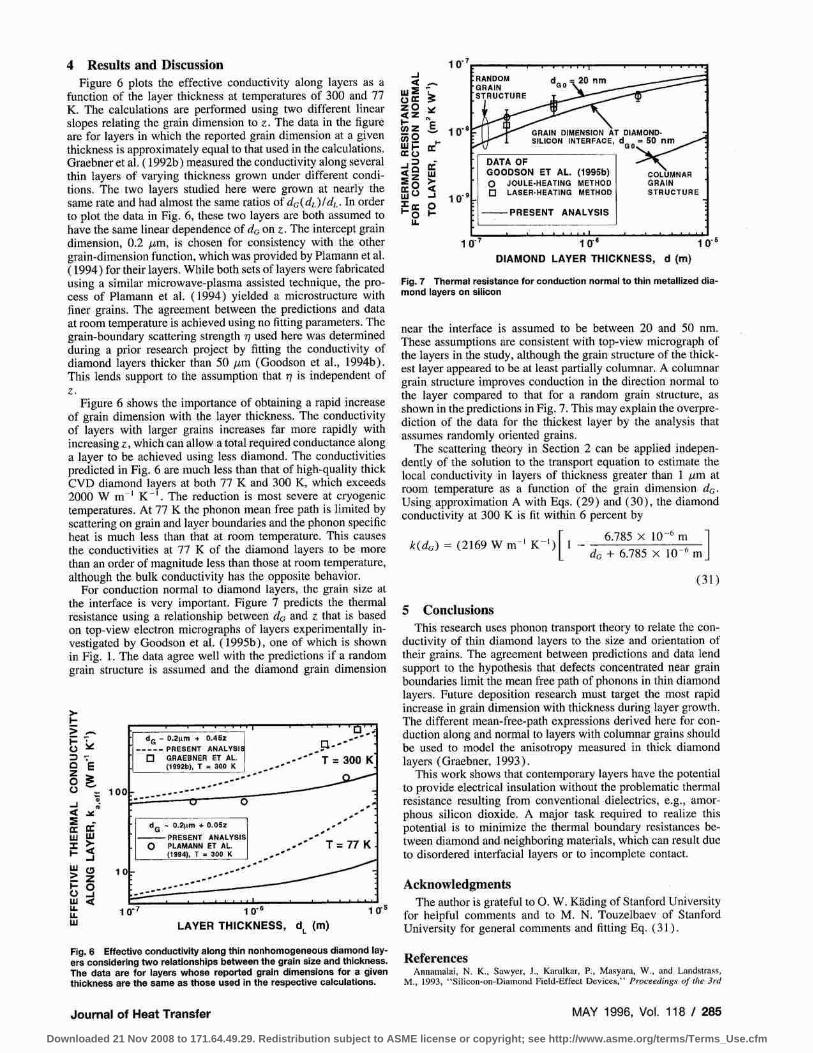
For conduction normal to diamond layers, the grain size at the interface is very important. Figure 7 predicts the thermal resistance using a relationship between da and z that is based on top-view electron micrographs of layers experimentally in- vestigated by Goodson et al. (1995b), one of which is shown in Fig. 1. The data agree well with the predictions if a random grain structure is assumed and the diamond grain dimension
>.
T E
Z
0 : 100
W
I- -,I
, o I -
tu <
UJ 10-7
d G - O .2gm + 0 . 4 5 z - - ' - - P R E S E N T ANALYSI~ ~ ' ' ' ' ' " :
[ ] GRAEBNER ET AL. . ' ' " ' T = 300 K' (1992b), T = 300 K . . . . - "
; G ~ 0 . 2 g m + O.05z . ° * S *
P R E S E N T A N A L Y S I S * ° PLAMANN ET AL, o ' ' ' " T = 77 K (1994), T = 300 K . ~ * "
:=:=...: i i i i i i i i I I I . . . . . .
1 0 "s ffs
LAYER THICKNESS, d L (m)
Fig, 6 Effective conductivity along thin nonhomogeneous diamond lay- ers considering two relationships between the grain size and thickness, The data are for layers whose reported grain dimensions for a given thickness are the same as those used in the respective calculations.
10-7 f R A N O O ; ' ' ' tGRAiN ao % - ~ - ~
z ,~, 10""F I I ~ ~ N DIMENSION AT DIAMOND- 0
[ GOODSON ET AL. (1995b) COLUMNAR ~ ,~ r o JOULE-HEATING METHOD GRAIN
0 ~ 1 0 "9 | [ ] LASERH- EATING M E T H O D STRUCTURE
I I I I I I I I I I I I I . . . . . 1 0 -7 1 0 4 0 "G
DIAMOND LAYER THICKNESS, d (m)
Fig. 7 Thermal resistance for conduction normal to thin metallized dia- mond layers on silicon
near the interface is assumed to be between 20 and 50 nm. These assumptions are consistent with top-view micrograph of the layers in the study, although the grain structure of the thick- est layer appeared to be at least partially columnar. A columnar grain structure improves conduction in the direction normal to the layer compared to that for a random grain structure, as shown in the predictions in Fig. 7. This may explain the overpre- diction of the data for the thickest layer by the analysis that assumes randomly oriented grains.
The scattering theory in Section 2 can be applied indepen- dently of the solution to the transport equation to estimate the local conductivity in layers of thickness greater than 1 ~m at room temperature as a function of the grain dimension dG. Using approximation A with Eqs. (29) and (30), the diamond conductivity at 300 K is fit within 6 percent by
[ 6"785× 10-6m ] k(dc) = ( 2 1 6 9 W m ~ K - l ) 1 - d e + 6.785 × 10 6m
(31)
5 Conclus ions This research uses phonon transport theory to relate the con-
ductivity of thin diamond layers to the size and orientation of their grains. The agreement between predictions and data lend support to the hypothesis that defects concentrated near grain boundaries limit the mean free path of phonons in thin diamond layers. Future deposition research must target the most rapid increase in grain dimension with thickness during layer growth. The different mean-free-path expressions derived here for con- duction along and normal to layers with columnar grains should be used to model the anisotropy measured in thick diamond layers (Graebner, 1993).
This work shows that contemporary layers have the potential to provide electrical insulation without the problematic thermal resistance resulting from conventional dielectrics, e.g., amor- phous silicon dioxide. A major task required to realize this potential is to minimize the thermal boundary resistances be- tween diamond and neighboring materials, which can result due to disordered interracial layers or to incomplete contact.
Acknowledgments The author is grateful to O. W. K~iding of Stanford University
for helpful comments and to M. N. Touzelbaev of Stanford University for general comments and fitting Eq. (31 ).
References Annamatai, N. K., Sawyer, J., Karulkar, P., Masyara, W., and Landstrass,
M., 1993, "Silicon-on-Diamond Field-Effect Devices," Proceedings of the 3rd
Journa l of H e a t T ransfer M A Y 1996, Vol. 118 / 285
Downloaded 21 Nov 2008 to 171.64.49.29. Redistribution subject to ASME license or copyright; see http://www.asme.org/terms/Terms_Use.cfm

IUMRS International Conference on Advanced Materials, Tokyo, Japan, Aug. 31-Sept. 4.
Berman, R., 1976, Thermal Conduction in Solids, Oxford University Press, Oxford, United Kingdom, p. 23.
Brewster, M. Q., 1992, Thermal Radiative Transfer and Properties, Wiley, New York, Chap. 11, p. 232.
Chen, G., and Tien, C. L., 1993, "Thermal Conductivity of Quantum-Well Structures," J. Thermophysics and Heat Transfer, Vol. 7, pp. 311-318.
Flik, M. I., Choi, B. I., and Goodson, K. E., 1992, "Heat Transfer Regimes in Microstructures," ASME JOURNAL OF HEAT TRANSFER, Vol. 114, pp. 666-674.
Fuchs, K., 1938, "The Conductivity of Thin Metallic Films According to the Electron Theory of Metals," Proc. Cambridge Phil Soc., Vol. 34, pp. 100-108.
Goodson, K. E., Flik, M. I., Su, L. T., and Antoniadis, D. A., 1994a, "Prediction and Measurement of the Thermal Conductivity of AmoIphous Dielectric Layers," ASME JOURNAL OF HEAT TRANSFER, Vol. 116, pp. 317-324.
Goodson, K. E., Kading, O. W., and Zachai, R., 1994b, "Thermal Resistances at the Boundaries of CVD Diamond Layers in Electronic Systems," presented at the ASME Winter Annual Meeting, Chicago, IL, Nov. 11-18.
Goodson, K. E., 1995, "Impact of CVD Diamond Layers on the Thermal Engineering of Electronic Systems," Annual Review of Heat Transfer, Vol. VI, Begell House, New York, pp. 323-353.
Goodson, K. E., Flik, M. I., Su, L. T., and Antoniadis, D. A., 1995a, "Prediction and Measurement of Temperature Fields in Silicon-on-Insulator Electronic Cir- cuits," ASME JOURNAL OF HEAT TRANSFER, Vol. 117, pp. 574-581.
Goodson, K. E., Kfiding, O. W., ROsier, M., and Zachai, R., 1995b, "Experi- mental Investigation of Thermal Conduction Normal to Diamond-Silicon Bound- aries," J. Appl. Phys., Vol. 77, pp. 1385-1392.
Goodson, K. E., Kurabayashi, K., and Pease, R. F. W., 1995c, "Improved Heat Sinking for Laser-Diode Arrays Using Microchannels in CVD Diamond," Proceedings of the ASME National Heat Transfer Conference, Portland, OR, Aug. 5-9, S. S. Sadhal et al., eds., Vol. 3, pp. 187-192.
Graebner, J. E., Jin, S., Kammlott, G. W., Herb, J. A., and Gardinier, C. F., 1992a, "Unusually High Thermal Conductivity in Diamond Films," AppL Phys. Lett., Vol. 60, pp. 1576-1578.
Graebner, J. E., Mucha, J. A., Seibles, L., and Kammlott, G. W., 1992b, "The Thermal Conductivity of Chemical-Vapor-Deposited Diamond Films on Silicon," J. Appl. Phys., Vol. 71, pp. 3143-3146.
Graebner, J. E., 1993, "Thermal Conductivity of CVD Diamond: Techniques and Results," Diamond Films and Technology, Vol. 3, pp. 77-130.
Heatherington, A. V., Wort, C. J. H., and Southworth, P., 1990, "Crystalline Perfection of Chemical Vapor Deposited Diamond Films," J. Materials Research, Vol. 5, pp. 1591-1594.
Joshi, A. A., and Majumdar, A., i993, "Transient Ballistic and Diffusive Phonon Heat Transport in Thin Films," J. Appl. Phys., Vol. 74, pp. 31-39.
K~ding, O. W., Matthias, E., Zachai, R., FfiBer, H. J., and Mtlnziger, P., 1993, ' 'Thermal Diffusivities of Thin Diamond Films on Silicon," Diamond and Related Materials, Vol. 2, pp. 1185-1190.
Kfiding, O. W., R6sler, M., Zachai, R., and F~JBer, H.-J., 1994, "Lateral Thermal Diffusivity of Epitaxial Diamond Films," Diamond and Related Materials, Vol. 3, pp. 1175-1182.
Majumdar, A., 1993, "Microscale Heat Conduction in Dielectric Thin Films," ASME JOURNAL OF HEAT TRANSFER, Vol. 115, p. 7.
Morelli, D. T., Uher, C., and Robinson, C. J, 1993, "Transmission of Phonons Through Grain Boundaries in Diamond Films," Appl. Phys. Lett., Vol. 62, pp. 1085-1087.
Peierls, R. E., 1955, Quantum Theory of Solids, Oxford University Press, New York, Chaps. 1 and 2.
Plamann, K., Foumier, D., Anger, E., and Gicquel, A., 1994, "Photothermal Examination of the Heat Diffusion Inhomogeneity in Diamond Films of Sub- micron Thickness," Diamond and Related Materials, Vol. 3, pp. 752-756.
Ravi, K. V., and Landstrass, M. I., 1989, "Silicon on Insulator Technology Using CVD Diamond," Proceedings of the First International Symposium on Diamond and Diamond-Like Films, J. P. Dismukes et aL, eds., The Electrochemi- cal Society, Pennington, NJ, pp. 24-37.
ROsier, M., Zachai, R., FtiBer, H.-J., Jiang, X., and Klages, C.-P., 1993, "Struc- tural Properties of Heteroepitaxial Diamond on Silicon," Proceedings of the 2nd International Conference on the Applications of Diamond Films and Related Materials, M. Yoshikawa et al., eds., MYU Press, Tokyo, Japan, pp. 691-696.
Sondheimer, E. H., 1952, "The Mean Free Path of Electrons in Metals," Advances in Physics, Vol. 1, pp. 1-42.
Stoner, B. R., Ma, G.-H. M., Wolter, S. D., and Glass, J. T., 1992, "Character- ization of Bias-Enhanced Nucleation of Diamond on Silicon by in Vacno Surface Analysis and Transmission Electron Microscopy," Phys. Rev. B, Vol. 45, pp. 11067-11084.
Swartz, E. T., and Pohl, R. O., 1989, "Thermal Boundary Resistance," Rev. Mod. Phys., Vol. 61, pp. 605-668.
286 / Voh 118, MAY 1996 Transactions of the ASME
Downloaded 21 Nov 2008 to 171.64.49.29. Redistribution subject to ASME license or copyright; see http://www.asme.org/terms/Terms_Use.cfm