
Theory of Electron, Phonon and Spin Transport in Nanoscale ...
30
HATEF SADEGHI, 2018, NANOTECHNOLOGY, 29, 373001 1 Theory of Electron, Phonon and Spin Transport in Nanoscale Quantum Devices Hatef Sadeghi Physics Department, Lancaster University, Lancaster LA1 4YB, UK At the level of fundamental science, it was recently demonstrated that molecular wires can mediate long-range phase-coherent tunnelling with remarkably low attenuation over a few nanometre even at room temperature. Furthermore, a large mean free path has been observed in graphene and other graphene-like two-dimensional materials. These create the possibility of using quantum and phonon interference to engineer electron and phonon transport through nanoscale junctions for wide range of applications such as molecular switches, sensors, piezoelectricity, thermoelectricity and thermal management. To understand transport properties of such devices, it is crucial to calculate their electronic and phononic transmission coefficients. The aim of this tutorial article is to outline the basic theoretical concepts and review the state-of-the-art theoretical and mathematical techniques to treat electron, phonon and spin transport in nanoscale molecular junctions. This helps not only to explain new phenomenon observed experimentally but also provides a vital design tool to develop novel nanoscale quantum devices. Index Terms—Molecular electronics, Nanoelectronics, Theory and modelling, Quantum interference, Phonon interference I. I NTRODUCTION:MOLECULAR ELECTRONICS T HE silicon-based semiconductor industry is facing a grave problem because of the performance limits imposed on semiconductor devices when miniaturized to nanoscale [1]. To counter this problem, new nanoscale materials such as car- bon nanotubes, graphene and transition metal dichalcogenide monolayers have been proposed [2]. Alternatively, the idea of using single molecules as building blocks to design and fabricate molecular electronic components has been around for more than 40 years [3], but only recently has it attracted huge scientific interest to explore their unique properties and opportunities. Molecular electronics including self-assembled monolayers [4] and single-molecule junctions [5] are of inter- est not only for their potential to deliver logic gates [6], sensors [7], and memories [8] with ultra-low power requirements and sub-10-nm device footprints, but also for their ability to probe room-temperature quantum properties at the molecular scale such as quantum interference [9] and thermoelectricity [10, 11]. There are five main area of research in molecular- scale electronics [5] namely: molecular mechanics, molecular optoelectronics, molecular electronics, molecular spintronics and molecular thermoelectrics. By studying electron and phonon transport across a junction consisting of two or more electrodes connected to a single or few hundred molecules, one could study the electrical and mechanical properties of nanoscale junctions such as molec- ular electronic building blocks, sensors, molecular spintronic, thermoelectric, piezoelectric and optoelectronic devices. For example, when a single molecule is attached to metallic electrodes, de Broglie waves of electrons entering the molecule from one electrode and leaving from the other form a complex interference pattern inside the molecule. These patterns could be utilized to optimize the single-molecule device performance e-mail: [email protected]; [email protected] Published in Nanotechnology, 2018, Volume 29, Number 37, Page 373001. DOI: 10.1088/1361-6528/aace21 Corresponding author: H. Sadeghi [6]. In addition, the potential of such junctions for removing heat from nanoelectronic devices (thermal management) and thermoelectrically converting waste heat into electricity has re- cently been recognized [10]. Indeed, electrons passing through single molecules have been demonstrated to remain phase coherent, even at room temperature. In this tutorial, the aim is to outline the basic theoretical concepts and review theoretical and mathematical techniques to model electron, phonon and spin transport in nanoscale molecular junctions. This helps not only to understand the experimental observations but also provides a vital design tool to develop strategies for molecular electronic building blocks, thermoelectric devices and sensors. Transport on the molecular scale: Any nanoscale device consists of two or more electrodes (leads) connected to a scattering region (figure 1). Electrodes are perfect wave- guides where electrons and phonons can transmit without any scattering. The main scattering occurs either at the interface to leads or inside scattering region. The goal is to understand the electrical and vibrational properties of nano and molecular junctions where a nanoscale scatter or a molecule is bonded to electrodes with strong or weak coupling in the absence or presence of surroundings, such as an electric field (e.g. gate and bias voltages or local charge), a magnetic field, a laser beam or a molecular environment (e.g. water, gases, biological spices, donors and acceptors). There are different approaches to study the electronic and vibrational properties of molecular junctions such as semi-classical methods [12–14], kinetic theory of quantum transport [15], scattering theory [16] and master equation approach [17]. In this paper, our focus is mostly on the scattering theory based on the Green’s function formalism and the master equation approach. Here, we begin with the Schr¨ odinger equation and relate it to the physical description of a matter at the nano and molecular scale. Then we will discuss the definition of the current using the time-dependent Schr¨ odinger equation and introduce density functional theory (DFT) and a tight binding description of quantum system. The scattering theory and non-
Transcript of Theory of Electron, Phonon and Spin Transport in Nanoscale ...

HATEF SADEGHI, 2018, NANOTECHNOLOGY, 29, 373001 1
Theory of Electron, Phonon and Spin Transportin Nanoscale Quantum Devices
Hatef SadeghiPhysics Department, Lancaster University, Lancaster LA1 4YB, UK
At the level of fundamental science, it was recently demonstrated that molecular wires can mediate long-range phase-coherenttunnelling with remarkably low attenuation over a few nanometre even at room temperature. Furthermore, a large mean free pathhas been observed in graphene and other graphene-like two-dimensional materials. These create the possibility of using quantum andphonon interference to engineer electron and phonon transport through nanoscale junctions for wide range of applications such asmolecular switches, sensors, piezoelectricity, thermoelectricity and thermal management. To understand transport properties of suchdevices, it is crucial to calculate their electronic and phononic transmission coefficients. The aim of this tutorial article is to outlinethe basic theoretical concepts and review the state-of-the-art theoretical and mathematical techniques to treat electron, phonon andspin transport in nanoscale molecular junctions. This helps not only to explain new phenomenon observed experimentally but alsoprovides a vital design tool to develop novel nanoscale quantum devices.
Index Terms—Molecular electronics, Nanoelectronics, Theory and modelling, Quantum interference, Phonon interference
I. INTRODUCTION: MOLECULAR ELECTRONICS
THE silicon-based semiconductor industry is facing agrave problem because of the performance limits imposed
on semiconductor devices when miniaturized to nanoscale [1].To counter this problem, new nanoscale materials such as car-bon nanotubes, graphene and transition metal dichalcogenidemonolayers have been proposed [2]. Alternatively, the ideaof using single molecules as building blocks to design andfabricate molecular electronic components has been aroundfor more than 40 years [3], but only recently has it attractedhuge scientific interest to explore their unique properties andopportunities. Molecular electronics including self-assembledmonolayers [4] and single-molecule junctions [5] are of inter-est not only for their potential to deliver logic gates [6], sensors[7], and memories [8] with ultra-low power requirementsand sub-10-nm device footprints, but also for their ability toprobe room-temperature quantum properties at the molecularscale such as quantum interference [9] and thermoelectricity[10, 11]. There are five main area of research in molecular-scale electronics [5] namely: molecular mechanics, molecularoptoelectronics, molecular electronics, molecular spintronicsand molecular thermoelectrics.
By studying electron and phonon transport across a junctionconsisting of two or more electrodes connected to a single orfew hundred molecules, one could study the electrical andmechanical properties of nanoscale junctions such as molec-ular electronic building blocks, sensors, molecular spintronic,thermoelectric, piezoelectric and optoelectronic devices. Forexample, when a single molecule is attached to metallicelectrodes, de Broglie waves of electrons entering the moleculefrom one electrode and leaving from the other form a complexinterference pattern inside the molecule. These patterns couldbe utilized to optimize the single-molecule device performance
e-mail: [email protected]; [email protected] in Nanotechnology, 2018, Volume 29, Number 37, Page 373001.DOI: 10.1088/1361-6528/aace21Corresponding author: H. Sadeghi
[6]. In addition, the potential of such junctions for removingheat from nanoelectronic devices (thermal management) andthermoelectrically converting waste heat into electricity has re-cently been recognized [10]. Indeed, electrons passing throughsingle molecules have been demonstrated to remain phasecoherent, even at room temperature. In this tutorial, the aim isto outline the basic theoretical concepts and review theoreticaland mathematical techniques to model electron, phonon andspin transport in nanoscale molecular junctions. This helpsnot only to understand the experimental observations but alsoprovides a vital design tool to develop strategies for molecularelectronic building blocks, thermoelectric devices and sensors.
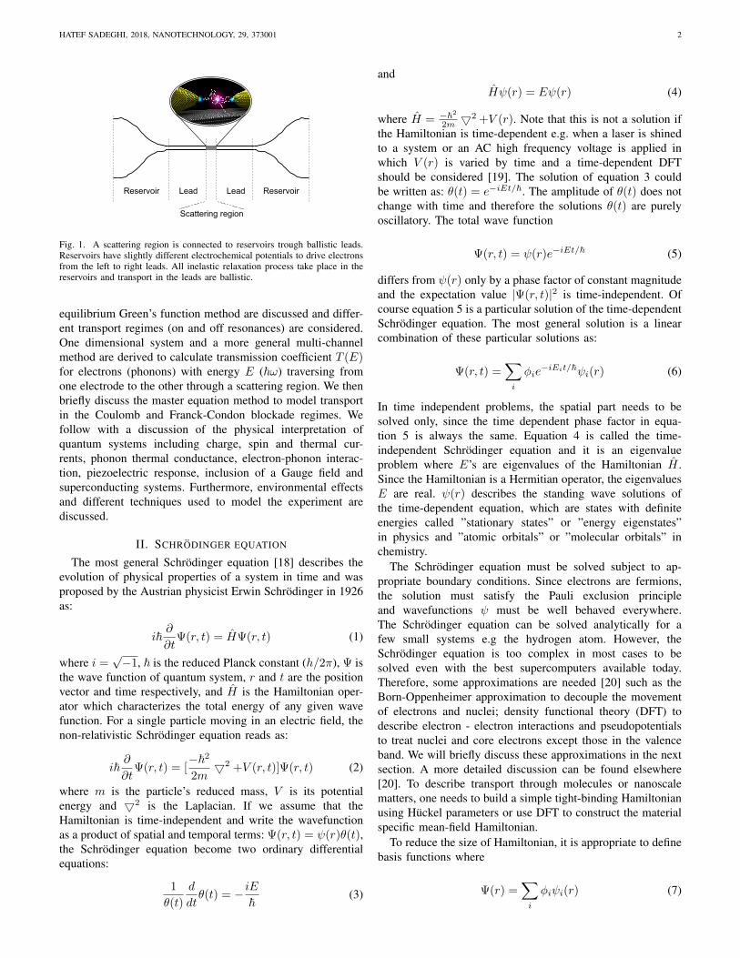
Transport on the molecular scale: Any nanoscale deviceconsists of two or more electrodes (leads) connected to ascattering region (figure 1). Electrodes are perfect wave-guides where electrons and phonons can transmit without anyscattering. The main scattering occurs either at the interfaceto leads or inside scattering region. The goal is to understandthe electrical and vibrational properties of nano and molecularjunctions where a nanoscale scatter or a molecule is bondedto electrodes with strong or weak coupling in the absenceor presence of surroundings, such as an electric field (e.g.gate and bias voltages or local charge), a magnetic field, alaser beam or a molecular environment (e.g. water, gases,biological spices, donors and acceptors). There are differentapproaches to study the electronic and vibrational propertiesof molecular junctions such as semi-classical methods [12–14],kinetic theory of quantum transport [15], scattering theory [16]and master equation approach [17]. In this paper, our focus ismostly on the scattering theory based on the Green’s functionformalism and the master equation approach.
Here, we begin with the Schrodinger equation and relateit to the physical description of a matter at the nano andmolecular scale. Then we will discuss the definition of thecurrent using the time-dependent Schrodinger equation andintroduce density functional theory (DFT) and a tight bindingdescription of quantum system. The scattering theory and non-
HATEF SADEGHI, 2018, NANOTECHNOLOGY, 29, 373001 2
Fig. 1. A scattering region is connected to reservoirs trough ballistic leads.Reservoirs have slightly different electrochemical potentials to drive electronsfrom the left to right leads. All inelastic relaxation process take place in thereservoirs and transport in the leads are ballistic.
equilibrium Green’s function method are discussed and differ-ent transport regimes (on and off resonances) are considered.One dimensional system and a more general multi-channelmethod are derived to calculate transmission coefficient T (E)for electrons (phonons) with energy E (~ω) traversing fromone electrode to the other through a scattering region. We thenbriefly discuss the master equation method to model transportin the Coulomb and Franck-Condon blockade regimes. Wefollow with a discussion of the physical interpretation ofquantum systems including charge, spin and thermal cur-rents, phonon thermal conductance, electron-phonon interac-tion, piezoelectric response, inclusion of a Gauge field andsuperconducting systems. Furthermore, environmental effectsand different techniques used to model the experiment arediscussed.
II. SCHRODINGER EQUATION
The most general Schrodinger equation [18] describes theevolution of physical properties of a system in time and wasproposed by the Austrian physicist Erwin Schrodinger in 1926as:
i~∂
∂tΨ(r, t) = HΨ(r, t) (1)
where i =√−1, ~ is the reduced Planck constant (h/2π), Ψ is
the wave function of quantum system, r and t are the positionvector and time respectively, and H is the Hamiltonian oper-ator which characterizes the total energy of any given wavefunction. For a single particle moving in an electric field, thenon-relativistic Schrodinger equation reads as:
i~∂
∂tΨ(r, t) = [
−~2
2m52 +V (r, t)]Ψ(r, t) (2)
where m is the particle’s reduced mass, V is its potentialenergy and 52 is the Laplacian. If we assume that theHamiltonian is time-independent and write the wavefunctionas a product of spatial and temporal terms: Ψ(r, t) = ψ(r)θ(t),the Schrodinger equation become two ordinary differentialequations:
1
θ(t)
d
dtθ(t) = − iE
~(3)
andHψ(r) = Eψ(r) (4)
where H = −~2
2m 52 +V (r). Note that this is not a solution if
the Hamiltonian is time-dependent e.g. when a laser is shinedto a system or an AC high frequency voltage is applied inwhich V (r) is varied by time and a time-dependent DFTshould be considered [19]. The solution of equation 3 couldbe written as: θ(t) = e−iEt/~. The amplitude of θ(t) does notchange with time and therefore the solutions θ(t) are purelyoscillatory. The total wave function
Ψ(r, t) = ψ(r)e−iEt/~ (5)
differs from ψ(r) only by a phase factor of constant magnitudeand the expectation value |Ψ(r, t)|2 is time-independent. Ofcourse equation 5 is a particular solution of the time-dependentSchrodinger equation. The most general solution is a linearcombination of these particular solutions as:
Ψ(r, t) =∑i
φie−iEit/~ψi(r) (6)
In time independent problems, the spatial part needs to besolved only, since the time dependent phase factor in equa-tion 5 is always the same. Equation 4 is called the time-independent Schrodinger equation and it is an eigenvalueproblem where E’s are eigenvalues of the Hamiltonian H .Since the Hamiltonian is a Hermitian operator, the eigenvaluesE are real. ψ(r) describes the standing wave solutions ofthe time-dependent equation, which are states with definiteenergies called ”stationary states” or ”energy eigenstates”in physics and ”atomic orbitals” or ”molecular orbitals” inchemistry.
The Schrodinger equation must be solved subject to ap-propriate boundary conditions. Since electrons are fermions,the solution must satisfy the Pauli exclusion principleand wavefunctions ψ must be well behaved everywhere.The Schrodinger equation can be solved analytically for afew small systems e.g the hydrogen atom. However, theSchrodinger equation is too complex in most cases to besolved even with the best supercomputers available today.Therefore, some approximations are needed [20] such as theBorn-Oppenheimer approximation to decouple the movementof electrons and nuclei; density functional theory (DFT) todescribe electron - electron interactions and pseudopotentialsto treat nuclei and core electrons except those in the valenceband. We will briefly discuss these approximations in the nextsection. A more detailed discussion can be found elsewhere[20]. To describe transport through molecules or nanoscalematters, one needs to build a simple tight-binding Hamiltonianusing Huckel parameters or use DFT to construct the materialspecific mean-field Hamiltonian.
To reduce the size of Hamiltonian, it is appropriate to definebasis functions where
Ψ(r) =∑i
φiψi(r) (7)
HATEF SADEGHI, 2018, NANOTECHNOLOGY, 29, 373001 3
The wavefunction can then be represented by a column vector|φ〉 consisting of the expansion coefficients φi. The time-independent Schrodinger equation could be written as a matrixequation:
[H]|φ〉 = E[S]|φ〉 (8)
whereSij = 〈i|j〉 =
∫drψ∗j (r)ψi(r) (9)
andHij = 〈i|H|j〉 =
∫drψ∗j (r)Hψi(r) (10)
The evaluation of these integrals is the most time-consumingstep, but once [H] and [S] are obtained, the eigenvalues Enand eigenvectors φn are easily calculated. If 〈i| and |j〉 areorthogonal then Sij = δij where δij is the Kronecker delta(δij = 1 if i = j and δij = 0 if i 6= j). Note that a system withthe Hamiltonian H and overlap matrix S obtained using non-orthogonal basis could be transformed to a new HamiltonianH = S−1/2×H×S−1/2 with orthogonal basis (S = I whereI is the Identity matrix.)
A. Density functional theory (DFT)
In order to understand the behavior of molecular electronicdevices, it is necessary to possess a reliable source of structuraland electronic information. A solution to the many bodyproblem has been sought by many generations of physicists.The task is to find the eigenvalues and eigenstates of the fullHamiltonian operator of a system consisting of nuclei andelectrons as shown in figure 2. Since this is not practicallypossible for the systems bigger than a few particles, some ap-proximations are needed. The atomic masses are roughly threeorders of magnitudes bigger than the electron mass, hence theBorn-Oppenheimer approximation [20] can be employed todecouple the electronic wave function and the motion of thenuclei. In other words, we solve the Schrodinger equation forthe electronic degrees of freedom only. Once we know theelectronic structure of a system, we can calculate classicalforces on the nuclei and minimize these forces to find theground-state geometry (figure 2a).
Once the Schrodinger equation was solved, the wavefunc-tion is known and all physical quantities of intereste couldbe calculated. Although the Born-Oppenheimer approximationdecouple the electronic wave function and the motion of thenuclei, the electronic part of the problem has reduced tomany interacting particles problem which even for modestsystem sizes i.e. a couple of atoms, its diagonalization ispractically impossible even on a modern supercomputer. Thevirtue of density functional theory DFT [20, 21] is that itexpresses the physical quantities in terms of the ground-statedensity and by obtaining the ground-state density, one can inprinciple calculate the ground-state energy. However, the exactform of the functional is not known. The kinetic term andinternal energies of the interacting particles cannot generallybe expressed as functionals of the density. The solution isintroduced by Kohn and Sham in 1965. According to Kohn andSham, the original Hamiltonian of the many body interacting
system can be replaced by an effective Hamiltonian of non-interacting particles in an effective external potential, whichhas the same ground-state density as the original system asillustrated in figure 2a. The difference between the energy ofthe non-interacting and interacting system is referred to theexchange correlation functional (figure 2a).
Exchange and correlation energy: There are numerousproposed forms for the exchange and correlation energy Vxcin the literature [20, 21]. The first successful - and yet simple- form was the Local Density Approximation (LDA) [21],which depends only on the density and is therefore a localfunctional. Then the next step was the Generalized GradientApproximation (GGA) [21], including the derivative of thedensity. It also contains information about the neighborhoodand therefore is semi-local. LDA and GGA are the twomost commonly used approximations to the exchange andcorrelation energies in density functional theory. There are alsoseveral other functionals, which go beyond LDA and GGA.Some of these functionals are tailored to fit specific needsof basis sets used in solving the Kohn-Sham equations and alarge category are the so called hybrid functionals (eg. B3LYP[22], HSE [23] and Meta hybrid GGA [22]), which includeexact exchange terms from Hartree-Fock. One of the latestand most universal functionals, the Van der Waals densityfunctional (vdW-DF [24]), contains non-local terms and hasproven to be very accurate in systems where dispersion forcesare important.
Pseudopotentials: Despite all simplifications shown in fig-ure 2, in typical systems of molecules which contain manyatoms, the calculation is still very large and has the po-tential to be computationally expensive. In order to reducethe number of electrons, one can introduce pseudopotentialswhich effectively remove the core electrons from an atom.The electrons in an atom can be split into two types: core andvalence, where core electrons lie within filled atomic shellsand the valence electrons lie in partially filled shells. Togetherwith the fact that core electrons are spatially localized aboutthe nucleus, only valence electron states overlap when atomsare brought together so that in most systems only valenceelectrons contribute to the formation of molecular orbitals.This allows the core electrons to be removed and replacedby a pseudopotential such that the valence electrons still feelthe same screened nucleon charge as if the core electronswere still present. This reduces the number of electrons in asystem dramatically and in turn reduces the time and memoryrequired to calculate properties of molecules that contain alarge number of electrons. Another benefit of pseudopotentialsis that they are smooth, leading to greater numerical stability.
Basis Sets: In order to turn the partial differential equations(e.g. the Schrodinger equation 1) into algebraic equationssuitable for efficient implementation on a computer, a setof functions (called basis functions) is used to represent theelectronic wave function. For a periodic system, the plane-wave basis set is natural since it is, by itself, periodic.However, to construct a tight-binding Hamiltonian, we need touse localised basis sets discussed in the next section, which arenot implicitly periodic. An example is a Linear Combinationof Atomic Orbital (LCAO) basis set which are constrained to

HATEF SADEGHI, 2018, NANOTECHNOLOGY, 29, 373001 4
Fig. 2. From many-body problem to density functional theory DFT. (a) Born-Oppenheimer approximation, Hohenberg-Kohn theorem and Kohn-Sham ansatz,(b) Schematic of the DFT self-consistency process.
be zero after some defined cut-off radius, and are constructedfrom the orbitals of the atoms.
Mean-field Hamiltonian from DFT: To obtain the groundstate mean-field Hamiltonian of a system from DFT, the calcu-lation is started by constructing the initial atomic configurationof the system. Depending on the applied DFT implementation,the appropriate pseudopotentials for each element which canbe different for every exchange-correlation functional might beneeded. Furthermore, a suitable choice of the basis set has tobe made for each element present in the calculation. The larger
the basis set, the more accurate our calculation - and, of course,the longer it will take. With a couple of test calculationswe can optimize the accuracy and computational cost. Otherinput parameters are also needed that set the accuracy of thecalculation such as the fineness and density of the k-grid pointsused to evaluate the integral([21, 25]). Then an initial chargedensity assuming no interaction between atoms is calculated.Since the pseudopotentials are known, this step is simple andthe total charge density will be the sum of the atomic densities.
The self-consistent calculation [21] (figure 2b) starts by
HATEF SADEGHI, 2018, NANOTECHNOLOGY, 29, 373001 5
calculating the Hartree and exchange correlation potentials.Since the density is represented in real space, the Hartreepotential is obtained by solving the Poisson equation with themulti-grid or fast Fourier-transform method. Then the Kohn-Sham equations are solved and a new density is obtained. Thisself-consistent iterations end when the necessary convergencecriteria are reached such as density matrix tolerance. Once theinitial electronic structure of a system was obtained, the forceson the nucleis is calculated and a new atomic configuration tominimize these forces obtained. New atomic configuration isthe new initial coordinate for the next self-consistent calcula-tion. This structural optimization is controlled by the conjugategradient method for finding the minimal ground state energyand the corresponding atomic configuration [21]. From theobtained ground state geometry of the system, the ground stateelectronic properties of the system such as the total energy,the binding energies between different part of the system, thedensity of states, the local density of states, the forces couldbe calculated. It is apparent that the DFT could potentiallyprovide an accurate description of the ground state propertiesof a system such as the total energy, the binding energy andthe geometrical structures. However, all electronic propertiesrelated to excited states are less accurate within DFT.
B. Tight-Binding Model
By expanding wave function over a finite set of atomicorbitals, Hamiltonian of a system can be written in a tight-binding model. The main idea is to represent the wave functionof a particle as a linear combination of some known localizedstates. A typical choice is to consider a linear combinationof atomic orbitals (LCAO). If the LCAO basis is used withinDFT, the Hamiltonian H and overlap S matrices used withinthe scattering calculation (section III) could be directly ex-tracted. However, if a plane-wave DFT code is used, a LCAO-like based Hamiltonian could be constructed using Wannierfunctions. For a periodic system where the wave function isdescribed by a Bloch function, equation 8 could be written as∑
β,c′
Hα,c;β,c′φβ,c′ = E∑β,c′
Sα,c;β,c′φβ,c′ (11)
where c and c′ are the neighboring identical cells containingstates α and
Hα,c;β,c′ = Hα,β(Rc −Rc′) (12)
and
φβ,c = φβeik.Rc . (13)
Equation 11 could be written as∑β
Hαβ(k)φβ = E∑β
Sαβ(k)φβ (14)
where
Hαβ(k) =∑c′
Hαβ(Rc −Rc′)eik(Rc−Rc′ ) (15)
and
Sαβ(k) =∑c′
Sαβ(Rc −Rc′)eik(Rc−Rc′ ) (16)
More generally, the single-particle tight-binding Hamiltonianin the Hilbert space formed by |Rα〉 could be written as:
H =∑α
(εα + eVα)|α〉〈α|+∑αβ
γαβ |α〉〈β| (17)
where εα is the corresponding on-site energy of the state |α〉,Vα is the electrical potential and γαβ are the hopping matrixelements between states |α〉 and |β〉.
Simple TB Hamiltonian: For conjugated hydrocarbons, theenergy of molecular orbitals associated with the π electronscould be determined by a very simple LCAO molecular or-bital method called Huckel molecular orbital method (HMO).Therefore, a simple TB description of system could be con-structed by assigning a Huckel parameter to on-site energyεα of each atom in the molecule connected to the nearestneighbours with a single Huckel parameter (hopping matrixelement) γαβ . Obviously, more complex TB models could bemade using HMO by taking the second, third, forth or morenearest neighbours hopping matrix elements into account.
It is worth mentioning that once a material specific LCAOmean-field DFT or a simple HMO Hamiltonians (describedin this section) were obtained, electron and spin transportproperties of a junction can be calculated.
1) Two level systemAs a simplest example, consider a close system of two
single-orbital sites with on-site energies ε and −ε coupled toeach other by the hoping integral γ. The Hamiltonian of such
system is written as: H =
(ε γγ∗ −ε
), so the Schrodinger
equation reads: (ε γγ∗ −ε
)(ψφ
)= E
(ψφ
)(18)
The eigenvalues E are calculated by solving det(H−EI) = 0
where I =
(1 00 1
)is the identity matrix.
E± = ±√ε2 + |γ|2 (19)
E− and E+ are called the bonding and anti-bonding states.
There must be two orthogonal eigenvectors(ψ+
φ+
)and
(ψ−φ−
)corresponding to each eigenvalue. By substituting equation 19into equation 18,
ψ±φ±
=γ
E± − ε=E± + ε
γ∗(20)
If ε = 0 and E = ±γ, simplest normalised eigenstates couldbe written as:(
ψ+
φ+
)=
1√2
(11
),
(ψ−φ−
)=
1√2
(1−1
)(21)
If γ = 0 and E = ±ε, the wave functions are fully localisedon each site:(
ψ+
φ+
)=
1√2
(01
),
(ψ−φ−
)=
1√2
(10
)(22)
HATEF SADEGHI, 2018, NANOTECHNOLOGY, 29, 373001 6
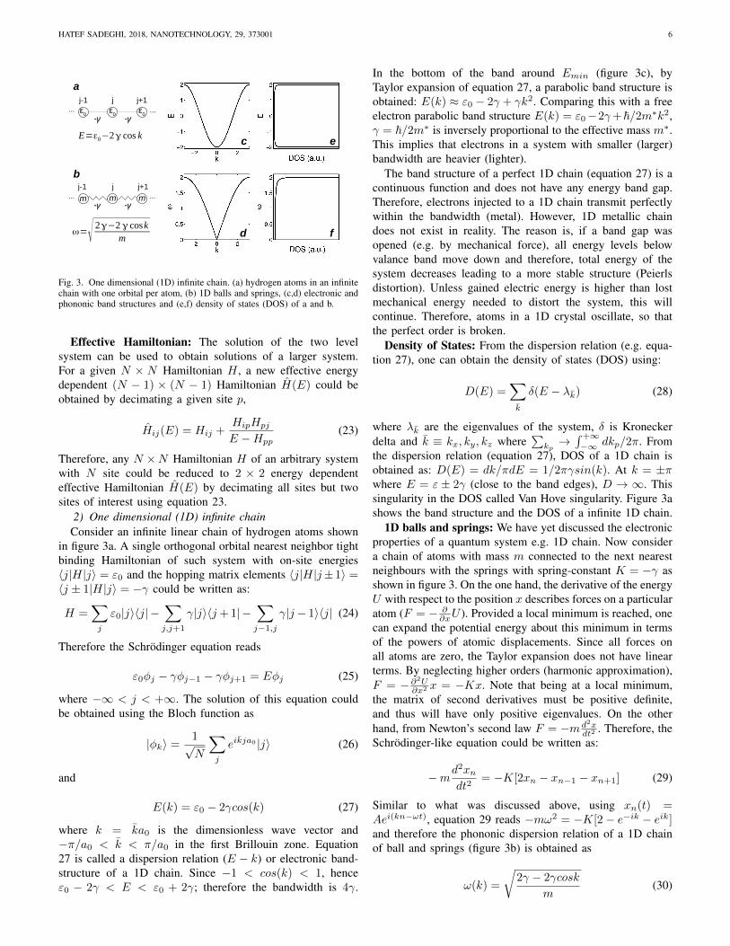
Fig. 3. One dimensional (1D) infinite chain. (a) hydrogen atoms in an infinitechain with one orbital per atom, (b) 1D balls and springs, (c,d) electronic andphononic band structures and (e,f) density of states (DOS) of a and b.
Effective Hamiltonian: The solution of the two levelsystem can be used to obtain solutions of a larger system.For a given N × N Hamiltonian H , a new effective energydependent (N − 1) × (N − 1) Hamiltonian H(E) could beobtained by decimating a given site p,
Hij(E) = Hij +HipHpj
E −Hpp(23)
Therefore, any N ×N Hamiltonian H of an arbitrary systemwith N site could be reduced to 2 × 2 energy dependenteffective Hamiltonian H(E) by decimating all sites but twosites of interest using equation 23.
2) One dimensional (1D) infinite chainConsider an infinite linear chain of hydrogen atoms shown
in figure 3a. A single orthogonal orbital nearest neighbor tightbinding Hamiltonian of such system with on-site energies〈j|H|j〉 = ε0 and the hopping matrix elements 〈j|H|j±1〉 =〈j ± 1|H|j〉 = −γ could be written as:
H =∑j
ε0|j〉〈j| −∑j,j+1
γ|j〉〈j + 1| −∑j−1,j
γ|j− 1〉〈j| (24)
Therefore the Schrodinger equation reads
ε0φj − γφj−1 − γφj+1 = Eφj (25)
where −∞ < j < +∞. The solution of this equation couldbe obtained using the Bloch function as
|φk〉 =1√N
∑j
eikja0 |j〉 (26)
and
E(k) = ε0 − 2γcos(k) (27)
where k = ka0 is the dimensionless wave vector and−π/a0 < k < π/a0 in the first Brillouin zone. Equation27 is called a dispersion relation (E − k) or electronic band-structure of a 1D chain. Since −1 < cos(k) < 1, henceε0 − 2γ < E < ε0 + 2γ; therefore the bandwidth is 4γ.
In the bottom of the band around Emin (figure 3c), byTaylor expansion of equation 27, a parabolic band structure isobtained: E(k) ≈ ε0 − 2γ + γk2. Comparing this with a freeelectron parabolic band structure E(k) = ε0−2γ+~/2m∗k2,γ = ~/2m∗ is inversely proportional to the effective mass m∗.This implies that electrons in a system with smaller (larger)bandwidth are heavier (lighter).
The band structure of a perfect 1D chain (equation 27) is acontinuous function and does not have any energy band gap.Therefore, electrons injected to a 1D chain transmit perfectlywithin the bandwidth (metal). However, 1D metallic chaindoes not exist in reality. The reason is, if a band gap wasopened (e.g. by mechanical force), all energy levels belowvalance band move down and therefore, total energy of thesystem decreases leading to a more stable structure (Peierlsdistortion). Unless gained electric energy is higher than lostmechanical energy needed to distort the system, this willcontinue. Therefore, atoms in a 1D crystal oscillate, so thatthe perfect order is broken.
Density of States: From the dispersion relation (e.g. equa-tion 27), one can obtain the density of states (DOS) using:
D(E) =∑k
δ(E − λk) (28)
where λk are the eigenvalues of the system, δ is Kroneckerdelta and k ≡ kx, ky, kz where
∑kp→∫ +∞−∞ dkp/2π. From
the dispersion relation (equation 27), DOS of a 1D chain isobtained as: D(E) = dk/πdE = 1/2πγsin(k). At k = ±πwhere E = ε ± 2γ (close to the band edges), D → ∞. Thissingularity in the DOS called Van Hove singularity. Figure 3ashows the band structure and the DOS of a infinite 1D chain.
1D balls and springs: We have yet discussed the electronicproperties of a quantum system e.g. 1D chain. Now considera chain of atoms with mass m connected to the next nearestneighbours with the springs with spring-constant K = −γ asshown in figure 3. On the one hand, the derivative of the energyU with respect to the position x describes forces on a particularatom (F = − ∂
∂xU ). Provided a local minimum is reached, onecan expand the potential energy about this minimum in termsof the powers of atomic displacements. Since all forces onall atoms are zero, the Taylor expansion does not have linearterms. By neglecting higher orders (harmonic approximation),F = −∂
2U∂x2 x = −Kx. Note that being at a local minimum,
the matrix of second derivatives must be positive definite,and thus will have only positive eigenvalues. On the otherhand, from Newton’s second law F = −md2x
dt2 . Therefore, theSchrodinger-like equation could be written as:
−md2xndt2
= −K[2xn − xn−1 − xn+1] (29)
Similar to what was discussed above, using xn(t) =Aei(kn−ωt), equation 29 reads −mω2 = −K[2− e−ik − eik]and therefore the phononic dispersion relation of a 1D chainof ball and springs (figure 3b) is obtained as
ω(k) =
√2γ − 2γcosk
m(30)

HATEF SADEGHI, 2018, NANOTECHNOLOGY, 29, 373001 7
Fig. 4. 1D finite chain and ring. The energy levels and corresponding wave functions or orbitals for 1D finite chain and ring. The phononic mode for a finitechain of balls and springs with mass m.
Comparing equations 27 and 30, it is apparent that equation 30is obtained by changing E → ω2 and ε0 → 2γ/m in equation27. ε0 = 2γ/m is the negative of sum of all off-diagonalterms of 1D chain TB Hamiltonian which make sense to satisfytranslational invariance. Therefore, Schrodinger equation-likerelation for phonons could be written as
ω2ψ = Dψ (31)
where D = −K/M is the dynamical matrix, M is the massmatrix and K is Hessian matrix calculated from the forcematrix.
3) One dimensional (1D) finite chain and ringTo analyse the effect of boundary conditions in the solution
of the Schrodinger equation, consider three examples shown infigure 4. As the first example, consider a 1D finite chain of Natoms. As a consequence of introducing boundary conditionsat the two ends of the chain, the energy levels and states areno longer continuous in the range of ε0 − 2γ < E < ε0 +2γ; instead there are discrete energy levels with correspondingstates in this range. This is obtained by writing the Schrodingerequation in 1 < j < N (equation 25) and at the boundariesj = 1 and j = N . At j = 1 the Schrodinger equation reads
ε0φ1 − γφ2 = Eφ1 (32)
and at j = Nε0φN − γφN−1 = EφN (33)
using the Bloch function φj = eikj + ce−ikj , the solution forthe 1D finite chain problem is obtained as:
φj =
√2
N + 1sin(
nπ
N + 1j) (34)
where n ∈ [1, ..., N ]. Similarly, solutions of 1D finite ring ofN atom could be obtained (figure 4) as:
φj =1√Ne
2nπN j (35)
where n ∈ [0, ..., N −1]. Clearly, the allowed energy levels of1D finite chain is different than 1D ring. This demonstrates thata small change in a molecular system may significantly affectthe energy levels and corresponding orbitals. This becomesmore important when few number of atoms was investigatede.g. the molecules, so two very similar molecules may showdifferent electronic properties.
Figure 4 also shows a solution for a phononic toy modelconsist of N ball connected to each other by springs withspring constant −γ.
φj = A cos(nπj
N− nπ
2N) (36)
where n ∈ [0, ..., N − 1], A = 1/√N for n = 0 and A =
1/√
2N , otherwise. Note that to satisfy translational invariancecondition, the diagonal terms in dynamical matrix are +2γexcept in the boundaries (j = 1 and j = N ) where they are+γ.
4) Two dimensional (2D) square and hexagonal latticesIn section II-B2, the band-structure and density of states
of a 1D chain were calculated. Now let’s consider two mostused 2D lattices: a square lattice where the unit-cell consistof one atom is connected to the first nearest neighbour in twodimensions (figure 5a) and a hexagonal lattice where a unitcell consist of two atoms is connected to the neighbouringcells in which first (second) atom in a cell is only connectedto the second (first) atom in any first nearest neighbour cell(figure 5b). The TB Hamiltonian and corresponding band-structure could be calculated [12–14] using equation 17 andthe Bloch wave function of the form Aeikxj+ikyl (figure 5).The Schrodinger equation for two dimensional square lattice(figure 5a) with on-site energies ε0 and hopping integrals γcould be written as:
ε0φj,l−γφj,l−1−γφj,l+1−γφj−1,l,−γφj+1,l = Eφj,l (37)
HATEF SADEGHI, 2018, NANOTECHNOLOGY, 29, 373001 8
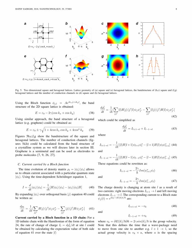
Fig. 5. Two dimensional square and hexagonal lattices. Lattice geometry of (a) square and (e) hexagonal lattices, the bandstructure of (b,c) square and (f,g)hexagonal lattices and the number of conduction channels in (d) square and (h) hexagonal lattices.
Using the Bloch function φj,l = Aeikxj+ikyl, the bandstructure of the 2D square lattice is obtained:
E = ε0 − 2γ(cos kx + cos ky) (38)
Using similar approach, the band structure of a hexagonallattice (e.g. graphene) could be obtained as:
E = ε0 ± γ√
1 + 4cos kx cos ky + 4cos2 ky (39)
Figures 5b,c,f,g show the bandstructure of the square andhexagonal lattices. The number of conduction channels (fig-ures 5d,h) could be calculated from the band structure ofa crystalline system as we will discuss later in section III.Graphene is a semimetal and can be used as electrodes toprobe molecules [7, 9, 26, 27].
C. Current carried by a Bloch function
The time evolution of density matrix ρt = |ψt〉〈ψt| allowsus to obtain current associated with a particular quantum state|ψt〉. Using the time-dependent Schrodinger equation 1,
I =d
dt|ψt〉〈ψt| =
1
i~[H|ψt〉〈ψt| − |ψt〉〈ψt|H] (40)
By expanding |ψt〉 over orthogonal basis |j〉 equation 40 couldbe written as:
dρtdt
=1
i~[∑jj′
H|j〉〈j′|ψjψ∗j′ −∑jj′
|j〉〈j′|Hψjψ∗j′ ] (41)
Current carried by a Bloch function in a 1D chain: For a1D infinite chain with the Hamiltonian of the form of equation24, the rate of change of charge Il = dρlt/dt at site l couldbe obtained by calculating the expectation value of both sideof equation 41 over the state |l〉
dρltdt
=1
i~[∑jj′
〈l|H|j〉〈j′|l〉ψjψ∗j′ −∑jj′
〈l|j〉〈j′|H|l〉ψjψ∗j′ ]
(42)which could be simplified as
dρltdt
= Il+1→l + Il−1→l (43)
where
Il+1→l = − 1
i~[〈l|H|l+1〉ψl+1ψ
∗l −〈l+1|H|l〉ψlψ∗l+1] (44)
and
Il−1→l = − 1
i~[〈l|H|l−1〉ψl−1ψ
∗l −〈l−1|H|l〉ψlψ∗l−1] (45)
These equations could be rewritten as:
Il+1→l = −2γ
~Im(ψ∗l+1ψl) (46)
andIl−1→l = −2γ
~Im(ψ∗l−1ψl) (47)
The charge density is changing at atom site l as a result oftwo currents: right moving electrons Il+1 → l and left movingelectrons Il−1 → l. The corresponding current to a Bloch stateψj(t) = eikj−iE(k)t/~ are:
Il+1→l = −vk (48)
andIl−1→l = +vk (49)
where vk = ∂E(k)/~∂k = 2γsin(k)/~ is the group velocity.Note that this defines the time that a wave-package needto move from one site to another e.g. l + 1 → l, so theactual group velocity is vk × a, where a is the spacing
HATEF SADEGHI, 2018, NANOTECHNOLOGY, 29, 373001 9
between the sites. Although the individual currents are non-zero and proportional to the group velocity, the total currentI = Il+1→l + Il−1→l for a pure Bloch state is zero due toan exact balance between left and right going currents. It isworth to mention that to simplify the notation, a Bloch stateeikj is often normalized with its current flux 1/
√vk calculated
from equations 48 and 49 to obtain a unitary current. Hencewe will mostly use a normalized Bloch state eikj/
√vk in
later derivations. Furthermore, one important consequence ofequations 46 and 47 is that if ψj = Aeikj +Be−ikj , althoughthe charge density ρj = |ψj |2 is oscillating by j, the current isnot oscillating by j and it is equal to the sum of the individualcurrents at site l only, Im(ψ∗l ψl+1) = |A|2sink − |B|2sinkdue to the Aeikl and Be−ikl.
Initial states are usually assumed to be stationary. However,if a non-stationary initial state was prepared in a closed (iso-lated) system such as a finite 1D chain of N atom, the chargedensity would be time-dependent (oscillatory) and therefore,current could be defined. As an example, for a system oftwo atoms coupled to each other by −γ, Hamiltonian readsH =
( 0 −γ−γ 0
). If the initial states are ψ1(t) =
(10
)and
ψ2(t) =(
01
)which are non-stationary states, the final state
is obtained ψ(t) = ψ1(t) + ψ2(t) =( cos(γt/~)isin(γt/~)
)which is
not stationary. For such a closed system, the current could beobtained from equations 44 and 45.
D. Parr-Pariser-Pople (PPP) Hamiltonian
Equation 17 described a non-interacting Hamiltonian whichcould also be written in the form of
H =∑i
εini +∑i,j,s
γijc†i,scj,s (50)
where i and j run over the orbitals centred on each site. For theorbital centred on site i and with spin s, c†i,s is the electroncreation operator that inserts an electron in state i and cj,sis the electron annihilation operator which takes an electronout of state i [12–14]. ni,s = c†i,scj,s is the electron numberoperator with ni =
∑s ni,s, εi is the energy of the orbital
relative to the chiral symmetry point and γi,j are hoppingintegrals. Electron-electron interactions are missing from thenon-interacting Hamiltonian (equation 50). In order to take theCoulomb electron-electron interaction into account, the Parr-Pariser-Pople (PPP) model can be used to write the interactingtight-binding Hamiltonian as
Hint = H +∑i
Uii(ni,↑ −1
2)(ni,↓ −
1
2)
+1
2
∑i,j 6=i
Uij(ni − 1)(nj − 1)(51)
where Uii and Uij are the on-site and long range Coulombinteractions, respectively given by the Ohno parametrization,
Uii = U0 (52)
and for i 6= j
Uij = U0[1 + (U0
e2/4πε0dij)2]−1/2 (53)
HOMO LUMO
Co-tunnelling
Se
qu
en
tia
l tu
nn
elli
ng
Off-resonance
On
-re
son
an
ce
Cro
ss o
ve
r
Cro
ss o
ve
r
Green's function to model transport
Master equation to model transport
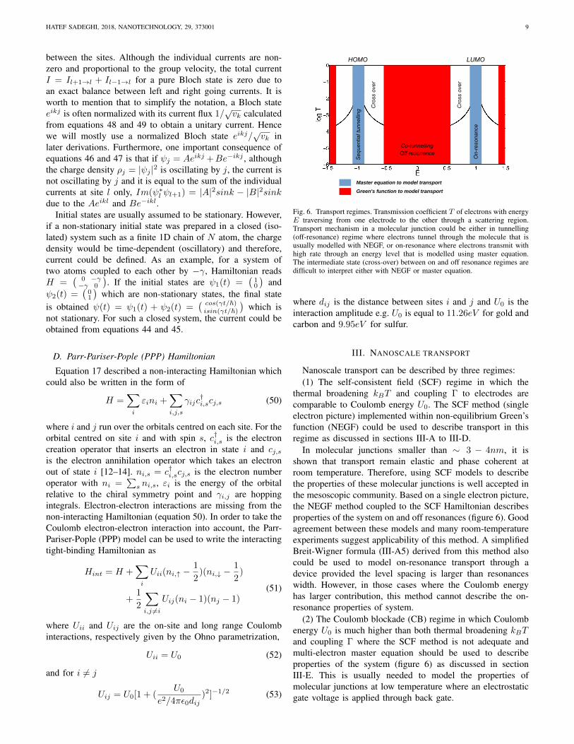
Fig. 6. Transport regimes. Transmission coefficient T of electrons with energyE traversing from one electrode to the other through a scattering region.Transport mechanism in a molecular junction could be either in tunnelling(off-resonance) regime where electrons tunnel through the molecule that isusually modelled with NEGF, or on-resonance where electrons transmit withhigh rate through an energy level that is modelled using master equation.The intermediate state (cross-over) between on and off resonance regimes aredifficult to interpret either with NEGF or master equation.
where dij is the distance between sites i and j and U0 is theinteraction amplitude e.g. U0 is equal to 11.26eV for gold andcarbon and 9.95eV for sulfur.
III. NANOSCALE TRANSPORT
Nanoscale transport can be described by three regimes:(1) The self-consistent field (SCF) regime in which the
thermal broadening kBT and coupling Γ to electrodes arecomparable to Coulomb energy U0. The SCF method (singleelectron picture) implemented within non-equilibrium Green’sfunction (NEGF) could be used to describe transport in thisregime as discussed in sections III-A to III-D.
In molecular junctions smaller than ∼ 3 − 4nm, it isshown that transport remain elastic and phase coherent atroom temperature. Therefore, using SCF models to describethe properties of these molecular junctions is well accepted inthe mesoscopic community. Based on a single electron picture,the NEGF method coupled to the SCF Hamiltonian describesproperties of the system on and off resonances (figure 6). Goodagreement between these models and many room-temperatureexperiments suggest applicability of this method. A simplifiedBreit-Wigner formula (III-A5) derived from this method alsocould be used to model on-resonance transport through adevice provided the level spacing is larger than resonanceswidth. However, in those cases where the Coulomb energyhas larger contribution, this method cannot describe the on-resonance properties of system.
(2) The Coulomb blockade (CB) regime in which Coulombenergy U0 is much higher than both thermal broadening kBTand coupling Γ where the SCF method is not adequate andmulti-electron master equation should be used to describeproperties of the system (figure 6) as discussed in sectionIII-E. This is usually needed to model the properties ofmolecular junctions at low temperature where an electrostaticgate voltage is applied through back gate.

HATEF SADEGHI, 2018, NANOTECHNOLOGY, 29, 373001 10
Fig. 7. Transport through an arbitrary scattering with Hamiltonian Hconnected two single channel electrodes.
(3) The intermediate regime (figure 6) in which theCoulomb energy U0 is comparable to the larger of the thermalbroadening kBT and coupling Γ. There is no simple approachto model this regime. Neither the SCF method nor masterequation could be used to well describe the transport inthis regime because SCF method does not do justice to thecharging, while the master equation does not do justice to thebroadening.
A. Transport through an arbitrary scattering region
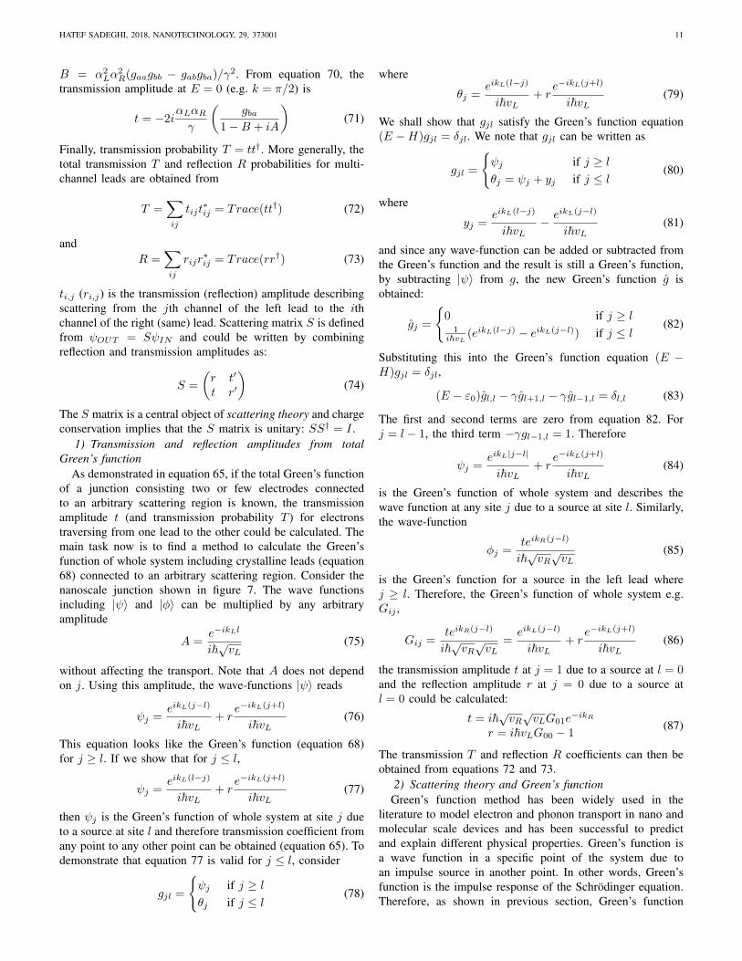
Consider the nanoscale junction of figure 7 where anarbitrary scattering region with Hamiltonian H connected totwo single channel electrodes. On-site energies and couplingin the left (right) lead L(R) are εL (εR) and −γL (−γR),respectively. The leads are connected to the site a and b ofthe scattering region with the couplings −αL and −αR. Theaim is to find the transmission t and reflection r amplitudesfor a Bloch wave normalized with its current flux eikLj/
√vL
traveling from the left to right (figure 7).If the wave function in the left and right leads and scat-
tering region are ψj = eikLj/√vL + re−ikLj/
√vL, φj =
teikRj/√vR and fj , respectively; the Schrodinger equation in
the left and right leads, the scattering region and connectionpoints could be written as:
εLψj − γLψj−1 − γLψj+1 = Eψj if j < 0L (54)
εLψ0 − γLψ−1 − αLfa = Eψ0 if j = 0L (55)∑i
Hjifi−αLψ0δja−αRφ0δjb = Efj if a 6 j 6 b (56)
εRφ0 − αRfb − γRφ1 = Eφ0 if j = 0R (57)
εRφj − γRφj−1 − γRφj+1 = Eφj if j > 0R (58)
From equations 54 and 58, the E−k relations (band-structure)in the left and right leads are obtained as:
E = εL − 2γLcos(kL) if j ≤ 0L
E = εR − 2γRcos(kR) if j ≥ 0R(59)
Equation 56 could be re-written as |f〉 = g |s〉 where g =(E−H)−1 is Green’s function and |s〉 called source which isa zero vector with non-zero elements in the connection pointsonly (at site j = a and j = b). For the junction in figure 7,|f〉 has only two non-zero elements due to the source,(
fafb
)=
(gaa gabgba gbb
)(sasb
)(60)
where sa = −αLψ0 and sb = −αRφ0. Furthermore, fromequations 55 and 57, the recurrence relation implies that:
−αLfa = −γLψ1
−αRfb = −γRφ−1(61)
andψ1 = 1√
vL(eikL − e−ikL) + ψ0e
−ikL
φ−1 = φ0e−ikR (62)
Hence, by substituting ψ1 and φ−1 in equation 61(fafb
)=
(− γLα2Le−ikL 0
0 − γRα2Re−ikR
)(sasb
)+
( γLαL√vL
2isin(kL)
0
) (63)
From equation 60 and 63,(sasb
)=
(gaa + γL
α2Le−ikL gab
gba gbb + γRα2Re−ikR
)−1
×( γLαL√vL
2isin(kL)
0
) (64)
Since sa = −αL(1 + r)/√vL and sb = −αRt/
√vR,
transmission t and reflection r amplitudes could be obtained.
t = i~√vLαLgL
(gbad
)gRαR
√vR (65)
where
gL,R =eikL,R
−γL,R(66)
is the surface Green’s function in the left and right leads atsites 0L and 0R (figure 7) and
d = 1− ΣLgaa − ΣRgbb + ΣLΣR(gaagbb − gabgba) (67)
where ΣL,R = α2L,RgL,R are called self-energies due to the
left and right contacts. The Green’s function in the surfaceof a semi-infinite lead (equation 66) can be obtained fromthe Green’s function of a doubly infinite crystalline lead. Forexample for the left electrode in figure 7, the Green’s functionof a doubly infinite crystalline chain is:
gLjl =eikL|j−l|
i~vL(68)
To calculate the Green’s function at site j = 0L due to asource at site l = 0L (the surface Green’s function), equation68 should vanish at site a (figure 7). This can be achieved byadding an appropriate wave function to equation 68,
gLjl =eikL|j−l|
i~vL− e−ikL(j−2a+l)
i~vL(69)
Hence, the Green’s function at site j = 0L due to a source atsite l = 0L is gL,R = −eikL,R/γL,R (equation 66). Assumingtwo identical leads (kL = kR = k and γL = γR = γ),equation 65 could be written as:
t = i2sin(k)e2ikαLαRγ
(gbad
)(70)
where d = 1 + ∆1 + i∆2 and ∆1 = Acos(k) + Bcos(2k),∆2 = Asin(k) + Bsin(2k), A = (gaaαL + gbbαR)/γ and
HATEF SADEGHI, 2018, NANOTECHNOLOGY, 29, 373001 11
B = α2Lα
2R(gaagbb − gabgba)/γ2. From equation 70, the
transmission amplitude at E = 0 (e.g. k = π/2) is
t = −2iαLαRγ
(gba
1−B + iA
)(71)
Finally, transmission probability T = tt†. More generally, thetotal transmission T and reflection R probabilities for multi-channel leads are obtained from
T =∑ij
tijt∗ij = Trace(tt†) (72)
andR =
∑ij
rijr∗ij = Trace(rr†) (73)
ti,j (ri,j) is the transmission (reflection) amplitude describingscattering from the jth channel of the left lead to the ithchannel of the right (same) lead. Scattering matrix S is definedfrom ψOUT = SψIN and could be written by combiningreflection and transmission amplitudes as:
S =
(r t′
t r′
)(74)
The S matrix is a central object of scattering theory and chargeconservation implies that the S matrix is unitary: SS† = I .
1) Transmission and reflection amplitudes from totalGreen’s function
As demonstrated in equation 65, if the total Green’s functionof a junction consisting two or few electrodes connectedto an arbitrary scattering region is known, the transmissionamplitude t (and transmission probability T ) for electronstraversing from one lead to the other could be calculated. Themain task now is to find a method to calculate the Green’sfunction of whole system including crystalline leads (equation68) connected to an arbitrary scattering region. Consider thenanoscale junction shown in figure 7. The wave functionsincluding |ψ〉 and |φ〉 can be multiplied by any arbitraryamplitude
A =e−ikLl
i~√vL(75)
without affecting the transport. Note that A does not dependon j. Using this amplitude, the wave-functions |ψ〉 reads
ψj =eikL(j−l)
i~vL+ r
e−ikL(j+l)
i~vL(76)
This equation looks like the Green’s function (equation 68)for j ≥ l. If we show that for j ≤ l,
ψj =eikL(l−j)
i~vL+ r
e−ikL(j+l)
i~vL(77)
then ψj is the Green’s function of whole system at site j dueto a source at site l and therefore transmission coefficient fromany point to any other point can be obtained (equation 65). Todemonstrate that equation 77 is valid for j ≤ l, consider
gjl =
ψj if j ≥ lθj if j ≤ l
(78)
where
θj =eikL(l−j)
i~vL+ r
e−ikL(j+l)
i~vL(79)
We shall show that gjl satisfy the Green’s function equation(E −H)gjl = δjl. We note that gjl can be written as
gjl =
ψj if j ≥ lθj = ψj + yj if j ≤ l
(80)
where
yj =eikL(l−j)
i~vL− eikL(j−l)
i~vL(81)
and since any wave-function can be added or subtracted fromthe Green’s function and the result is still a Green’s function,by subtracting |ψ〉 from g, the new Green’s function g isobtained:
gj =
0 if j ≥ l
1i~vL (eikL(l−j) − eikL(j−l)) if j ≤ l
(82)
Substituting this into the Green’s function equation (E −H)gjl = δjl,
(E − ε0)gl,l − γgl+1,l − γgl−1,l = δl,l (83)
The first and second terms are zero from equation 82. Forj = l − 1, the third term −γgl−1,l = 1. Therefore
ψj =eikL|j−l|
i~vL+ r
e−ikL(j+l)
i~vL(84)
is the Green’s function of whole system and describes thewave function at any site j due to a source at site l. Similarly,the wave-function
φj =teikR(j−l)
i~√vR√vL
(85)
is the Green’s function for a source in the left lead wherej ≥ l. Therefore, the Green’s function of whole system e.g.Gij ,
Gij =teikR(j−l)
i~√vR√vL
=eikL(j−l)
i~vL+ r
e−ikL(j+l)
i~vL(86)
the transmission amplitude t at j = 1 due to a source at l = 0and the reflection amplitude r at j = 0 due to a source atl = 0 could be calculated:
t = i~√vR√vLG01e
−ikR
r = i~vLG00 − 1(87)
The transmission T and reflection R coefficients can then beobtained from equations 72 and 73.
2) Scattering theory and Green’s functionGreen’s function method has been widely used in the
literature to model electron and phonon transport in nano andmolecular scale devices and has been successful to predictand explain different physical properties. Green’s function isa wave function in a specific point of the system due toan impulse source in another point. In other words, Green’sfunction is the impulse response of the Schrodinger equation.Therefore, as shown in previous section, Green’s function

HATEF SADEGHI, 2018, NANOTECHNOLOGY, 29, 373001 12
Fig. 8. Transport through a scatter connected to two 1D leads. For aBloch wave eikj/
√vk incident with a barrier, the wave is transmitted with
the amplitude of t (teikj/√vk) and reflected with the amplitude of r
(re−ikj/√vk). Using the surface Green’s function of the leads (g00 and
g11), the Hamiltonian of the scattering region in which bridge two leadsh and Dyson’s equation, the total Green’s function G could be calculated.The Green’s function could then be used to calculate the transmission t andreflection r amplitudes.
naturally carries all information about the wave-function evo-lution from one point to the other in a system [12–14, 28, 29].The Green’s function G of a system with N site described byHamiltonian H is defined as:
G = (EI −H)−1 (88)
where I is the identity matrix. Using the completeness condi-tion, ∑
n
|ψn〉〈ψn| = 1 (89)
The Green’s function could be written in terms of eigenstatesψn and eigenenergies λn of H ,
G =
N∑n=1
|ψn〉〈ψn|E − λn
(90)
and therefore the Green’s function element between point aand b is,
G(a, b) =
N∑n=1
ψn(a) ψ∗n(b)
E − λn(91)
Figure 8 shows how Green’s function could be used to calcu-late the transmission and reflection amplitudes in a simplestone dimensional system where two semi-infinite crystalline 1Dleads are connected to each other through coupling β (repre-senting the scattering region). The main question is what theamplitudes of the transmitted and reflected waves are? Thereare two main steps, first to calculate the total Green’s functionmatrix elements between sites 0 and 1 (G10) or 0 and 0 (G00);and secondly project these to the wavefunction to calculatetransmission t and reflection r amplitudes (equation 87). Forthis example, the transmission and reflection probabilities areobtained from T = tt† and R = rr†.
Dyson’s equation describes the exact Green’s function of asystem G = (g−1 − h)−1 in terms of the Green’s function of
non-interacting parts g and Hamiltonian that connects them h.As shown in figure 8, using the surface Green’s functions ofthe decoupled two semi-infinite leads g =
( g00 00 g11
)and the
Hamiltonian that couples them h, the total Green’s functioncould be obtained from Dyson’s equation (first step). Thesecond step is to use equation 87 to calculate t and r fromthe total green’s function G. It is worth to mention thatDyson’s equation could take different equivalent forms suchas G = (g−1 − h)−1, G = g + ghG or G = g + gV g whereV = (g−1 − h)−1.
3) Green’s function of N site finite chain and ringSimilar to the Green’s function of a semi-infinite chain
(equation 69), from the Green’s function of the doubly infinitecrystalline chain (equation 68), the Green’s function of N sitefinite chain and ring shown in figure 4 could be obtained [9]using appropriate boundary conditions as
gchainjl =
cos(k(N + 1− |j − l|))− cos(k(N + 1− j − l))2γsin(k)sin(k(N + 1))
(92)
and
gringjl =cos(k(N/2− |j − l|))2γsin(k)sin(kN/2))
(93)
These are useful equations to remember because they canhelp to understand quantum interference effects in simplemolecules. As an example, consider a ring of 6 sites (N = 6)e.g. benzene with on-site energies ε = 0 and hopping integralsγ = −1. In the middle of the energy band e.g. E = 0, fromthe dispersion relation of a 1D chain (equation II-B2), thewave vector is k = π/2. The Green’s function of benzenering between any site i and j at the middle of the band isobtained from equation 93 as:
gbenzenejl =cos(π2 (3− |j − l|))
2(94)
For any odd to odd (oo) or even to even (ee) connectivities (fig.4), (3−|j− l|) is an odd number and therefore gbenzeneoo or ee = 0.This is called destructive quantum interference because thetransmission between oo or ee sites are zero. In contrast, forany odd to even (oe) connectivity, (3 − |j − l|) is an evennumber and therefore gbenzeneoe 6= 0 which is called construc-tive quantum interference. This implies non-zero transmissionbetween any oe sites.
The Green’s function of the ring of 6 sites with on-site energies ε = 0 and hopping integrals γ can also beobtained by substituting its wavefunction (equation 35) intoequation 91. The eigenenergies of such system are: En =2γcos(2nπ/N) = [−2γ,−γ,−γ,+γ,+γ,+2γ]. The highestoccupied molecular orbital (HOMO) and lowest unoccupiedmolecular orbital (LUMO) levels are degenerate. At the middleof HOMO-LUMO gap E = EHL where EHL = (EH −EL)/2 = 0 and EH (EL) is the energy of HOMO (LUMO)level, the Green’s function is obtained from equation 91,
gringjl =1√N
2∑n=−3
ei2nπ
6 (j−l)
−En(95)

HATEF SADEGHI, 2018, NANOTECHNOLOGY, 29, 373001 13
It is convenient to introduce the notation,
gringjl =1√N
(gring1 /γ + gring2 /γ + gring3 /2γ) (96)
where
gringx = A(ei(xπ/3)(j−l) − ei(π+xπ/3)(j−l)) (97)
and A = [−1, 1, 1] for x = [1, 2, 3], respectively. For any ooor ee connectivities, j−l is an even number leading to a phaseshift of 2π in the second term of equation 97, that does notchange the sign of second term. Therefore the magnitude of thefirst and second terms in equation 97 are equal with oppositesign and therefore gring1 = 0, gring2 = 0, gring3 = 0 andgringoo or ee = 0 (the destructive quantum interference). This is aradical behaviour since contribution from all pares of HOMO– LUMO, HOMO-1 – LUMO+1 and HOMO-2 – LUMO+2states to the Green’s function are zero.
In contrast, for any oe connectivity, j− l is an odd numberleading to a phase shift of π in the second term of equation 97,that changes the sign of second term. Therefore, the magnitudeand sign of the first and second terms in equation 97 areequal, leading to non-zero values gringoe 6= 0 (the constructivequantum interference).
Consider a molecule which possesses only a HOMO ψH(l)of energy EH and a LUMO ψL(l) of energy EL, whoseGreen’s function from equation 91 is given by
glm(E) =ψH(l)ψ∗H(m)
E − EH+ψL(l)ψ∗L(m)
E − EL(98)
In this equation, ψH(l) and ψL(l) are the amplitudes of theHOMO and LUMO orbitals on connection site l, while ψH(m)and ψL(m) are the amplitudes of the HOMO and LUMOorbitals on connection site m. Since the core transmissioncoefficient for connectivity lm is given by τlm = (glm(E))2
a destructive interference feature occurs at an energy E givenby glm(E) = 0, or equivalently
ψH(l)ψ∗H(m)
ψL(l)ψ∗L(m)=E − EHE − EL
(99)
If the energy E at which the destructive interference featureoccurs lies within the HOMO-LUMO gap, then E −EH > 0and EL −E > 0. This can only occur if the left hand side ofequation 99 is positive and therefore the condition that a de-structive interference feature occurs within the HOMO-LUMOgap is that the orbital products must have the same sign. Con-versely, if they have opposite signs, there will be no destructiveinterference dip within the HOMO-LUMO gap. In the mostsymmetric case, where ψH(l)ψ∗H(m) = ψL(l)ψ∗L(m), thisyields E = (EL − EH)/2 and therefore the interference dipoccurs at the middle of the HOMO-LUMO gap. On the otherhand, if |ψH(l)ψ∗H(m)| << |ψL(l)ψ∗L(m)|, then E ' EHand the dip is close to the HOMO. In this case, for a realmolecule with many orbitals, the approximation of retainingonly the LUMO and HOMO breaks down, and the effect ofthe HOMO-1 should also be considered.
It is apparent from equation 98 that manipulating anti-resonances (e.g. due to the destructive quantum interference)
Fig. 9. Green’s function GF illustration and its relation with molecularorbitals MOs (wave functions) and transmission coefficient T . Huckel MOsof (a) benzene and (b) pyridine. All orbitals in the left (right) side of the dashedline in a and b are occupied (unoccupied). HOMO and LUMO are degeneratein benzene which are lifted by perturbation due to nitrogen in pyridine. Thecolour and radius of circles show sign and amplitude of MOs at each site,respectively. (c,d) illustrate GF due to injection point shown by green arrowsat two energies E = 0 (e.g. mid-gap) and E = 0.5 (e.g. close to the LUMOresonance). These are obtained using equation 90 and MOs in a and b.In all illustrations, the radius and colour of circles represent the amplitudeand sign of GF matrix elements between injection point (shown by greenarrows) and all collection points. Blue (red) represents positive (negative)numbers. If electron with energy E = 0 was injected from site shown bygreen arrows in c, the Green’s function matrix elements are zero for metacollection points but non zero for ortho and para collection points. Sincetransmission T is proportional to the module square of GF , zero transmissionis expected for meta connectivity whereas T is non-zero for para connectivityas shown in e. This is illustrated using GF plots in c and inset of e. From thegraphical visualisation of GF , the differences between transmission functionsare predictable. (d) illustrates GF for pyridine when electrons are injectedfrom site shown by green arrows in d and collected from any other points. (f)shows specific injection and collection points at E = 0 and E = 0.5. In bothcases the radius of GF increases by energy in agreement with transmissioncurve.
is easier than resonances. To manipulate a resonance, red-oxstate of a molecule should change whereas small environmen-tal effects such as an inhomogeneous charge distribution ornearby ions could lead to a significant change in the positionof anti-resonances.
Graphical illustration of Green’s function: As we dis-cussed in section III-A1, transmission coefficient T is pro-portional to the modules square of Green’s function. We alsoshowed that Green’s function can be obtained from the wavefunctions (molecular orbitals) using equation 90. To predictquantum interference from molecular orbitals (e.g. figure

HATEF SADEGHI, 2018, NANOTECHNOLOGY, 29, 373001 14
9a,b), a combination of two (HOMO and LUMO orbitals)or more orbitals need to be considered (section III-A3). Allof these contributions are naturally considered in Green’sfunction and therefore, by visualising the Green’s function, allinformation about quantum interference features are directlyaccessible. Graphical illustration of Green’s function alsoprovides more intuitive picture. This is like an intermediatestep between using molecular orbitals to predict transport andcarrying out a full transmission calculation. The graphicalillustration of Green’s function is also useful because it isnot trivial to predict differences between non-zero quantuminterference effects from molecular orbitals, whereas graphicalillustration of Green’s function provides this information (i.e.differences in the radius of circles in figure 9c,d).
Figure 9 shows two examples of polycyclic aromatic hy-drocarbons, benzene and pyridine. Six molecular orbitals andcorresponding eigenenergies due to six pz orbitals are shownin figure 9a,b. HOMO and LUMO states are degeneratein benzene. These degeneracies are lifted in pyridine dueto the presence of heteroatom (nitrogen). Consequently, themolecular orbitals are also affected.
Since Green’s function is the wave function due to a givensource, we can visualise Green’s function just like molecularorbitals for given electron injection point and energy. Exam-ples of Green’s function visualisation are illustrated in figure9c,d. Similar to wave functions visualisations, the radius andcolor of circles represent the amplitude and sign of Green’sfunction matrix elements, respectively due to a source in siteshown by the green arrows. Figures 9e,f show transmissioncoefficients of para and meta connectivities of benzene anda para connectivity of pyridine connected to two 1D leadsthrough a weak coupling. Corresponding Green’s functionillustrations are provided in the inset of figure 9e,f at twodifferent energies. Clearly, from the size of circles the mainfeatures of transmission is predictable. Therefore, one coulduse the Green’s function illustration of a molecule to predicttransport intuitively.
4) Density of states from Green’s FunctionThe density of states for a system with eigenvalues λ is
obtained from equation 28. However, having calculated theGreen’s function G from equation 90, the density of statescan be calculated. We note that a delta function δ(x−x0) canbe defined as the limit of a function which exhibits a sharppeak about x0 and whose integral over space is 1. For Instance
δ(x− x0) =1
πlimη−→0
(η
(x− x0)2 + η2) (100)
To prevent Green’s function to diverge at E = λ, equation 90can be written as
G =∑n
|ψn〉〈ψn|E − λn + iη
= Gr + iGi (101)
where η is a small number and
Gr =∑n
|ψn〉〈ψn|(E − λn)
(E − λn)2 + η2 (102)
and
Gi = −∑n
|ψn〉〈ψn|η
(E − λn)2 + η2 (103)
Since the eigenstates are orthonormal ψinψjn∗
= δij , we canfind the expression for the trace of the Green’s function whenη → 0 as trace(Gi) = −
∑n
η(E−λn)2+η2 = π
∑n δ(E−λn).
Therefore DOS is obtained,
D(E) = − 1
πtrace(Gi) (104)
5) Breit-Wigner formula (BWF)In the SCF regime, provided the coupling to electrodes
was weak enough, level broadening on resonances due toelectrodes was small enough and level spacing (differencesbetween the eigenenergies of a quantum system) was largeenough, the Green’s function gba in equation 65 for a systemdescribed by Hamiltonian H (figure 7) and energies close toan eigenvalue λm of H , is approximately
gba ≈ybya
E − λm(105)
where ya,b = fma,b and |fm〉 is the eigenvectors of H . Thisis a good approximation for E’s close to an eigenvalue λmif above mentioned conditions satisfied because the Green’sfunction g =
∑n|fn〉〈fn|E−λn terms in n 6= m are much smaller
than in n = m. This yields to on-resonance transmission T forelectrons with energy E passing through a molecule describedby a Lorentzian like transmission function called BWF:
T (E) =4ΓLΓR
(E − εn)2 + (ΓL + ΓR)2(106)
where εn = λ− σL − σR, σL,R =α2L,R
γL,Ry2a,bcos(kL,R) are the
real part of the self-energies. ΓL,R =α2L,R
γL,Ry2a,bsin(kL,R) are
the imaginary part of the self-energies (Σ = σ + iΓ) whichdescribe broadening due to the coupling of a molecular orbitalto the electrodes. λ is the eigenenergy of the molecular orbitalshifted slightly by an amount σ = σL+σR due to the couplingof the orbital to the electrodes. In this expression, y2
a and y2b
are the local DOS on the scattering region at the contact point.This formula shows that when the electron resonates with themolecular orbital (e.g. when E = εn), electron transmissionis a maximum. The formula is valid when the energy E ofelectron is close to an eigenenergy λ of the isolated molecule,and if the level spacing of the isolated molecule is largerthan (ΓL + ΓR). If ΓL = ΓR (a symmetric molecule attachedsymmetrically to the identical leads), T (E) = 1 on-resonance(E = εn).
If a bound state (e.g. a pendant group εp) is coupled(by coupling integral α) to a continuum of states, Fanoresonances could occur [30, 31]. Fano resonance contains ananti-resonance followed by a resonance with an asymmetricline profile in between. Fano resonance originates from a closecoexistence of resonant transmission and resonant reflection.This could be modeled by considering εn = λ − σL − σR +α2/(E − εp) in BWF. At E = εp, electron transmission isdestroyed (the electron anti-resonates with the pendant orbital)and at E = εn, the electron transmission is resonated by εn.The level spacing between this resonance and antiresonanceis proportional to α.
Two levels BWF: As we discussed above, if a levelbroadening is smaller than level spacing between resonances,

HATEF SADEGHI, 2018, NANOTECHNOLOGY, 29, 373001 15
BWF can be used in the weak coupling regime. In case of twodegenerate states, since these resonances can be close such thattheir level spacing is smaller than broadening, it is useful todrive a new form of BWF for two levels system. For a twolevels system, the Hamiltonian H in figure 7 is given by
H =
(ε1 VdVd ε2
)(107)
where ε1 and ε2 are the energy levels coupled to each otherby Vd. If ε1 (ε2) is weakly bonded to the left (right) lead, thetransmission coefficient T (E) could be obtained form equation65 as [32, 33]:
T (E) =4ΓLΓRV
2d
[(E − ε1 − σL + iΓL)(E − ε2 − σR + iΓR)− |Vd|2]2
(108)
where σL,R (ΓL,R) are the real (imaginary) part of the self-energies due to the left L and right R leads.
Wigner delay time: Wigner delay time is the measure oftime spent by an electron to pass from a scattering region of anopen system. If the transmission amplitude of a given systemt = |t|eiθ (106) is defined by its magnitude |t| and phase θ,the Wigner delay time describes the phase difference betweena scattered wave and a freely propagating one. Therefore, theWigner delay time τw = ~dθ/dE.
6) Open and close channels in leadsTo calculate the number of open conduction channels in a
3D arbitrary crystalline lead, it is useful to consider a simple2D cubic lattice with one orbital per site where each site isconnected to its first nearest neighbouring sites as shown inthe figure 5. For simplicity, consider a finite system in the ydirection Ny whereas the lattice is infinite in the x direction. Anormalized wave function and the band-structure of such struc-ture are calculated as ψmkx =
√2/(Ny + 1)sin(mπl/(Ny +
1))eikxj and E(kx) = ε0−2γcos(mπ/(Ny+1))+2γcos(kx),respectively. Similar to the one-dimensional case (sectionII-C), current is associated to each ψmkx since every mini-band corresponds to a Bloch state. ψmkx are called channels.If we assume that the injected electrons from each lead toany individual channel are uncorrelated, the conductance at agiven Fermi energy EF is given by G(EF ) = 2e2M(EF )/hwhere M(EF ) is the number of open conduction channels atEF . In a one-dimensional lead with one orbital per site, thereare either one open conduction channel or it is closed.
For the above quasi one dimensional system where x is thetransport direction and y is the transverse direction with Nyatomic sites, the Green’s function in the sites l and j due tothe source in the sites l′ and j′ could be written as:
glj,l′j′ =
Ny∑m=1
2
Ny + 1sin(
mπ
Ny + 1l)sin(
mπ
Ny + 1l′)eik
mx |j−j
′|
i~vmx(109)
where kmx is longitudinal momentum and vmx =∂E(kmx )/~∂kmx is the group velocity of channel m.Equation 109 could be re-written as:
glj,l′j′ =
Ny∑m=1
φmleik
mx |j−j
′|
i~vmxφ′m∗l (110)
TABLE IFOUR CLASSES OF POSSIBLE SCATTERING CHANNELS
left rightDecaying: Im(kmx ) > 0 Im(kmx ) < 0Propagating: Im(kmx ) = 0, vmx < 0 Im(kmx ) = 0, vmx > 0
Fig. 10. A sketch of a closed subspace B, in contact with subspace A throughcouplings W. XL denotes the surface of A connected to B. Subspace Bincludes some open subspaces connected to reservoirs shown by dotes.
where φml =√
2Ny+1sin( mπ
Ny+1 l). glj,l′j′ consists of the sum
of all allowed longitudinal modes eikmx j weighted by the
corresponding transverse components φml . Note that for agiven E, kmx could be both real and imaginary. If kmx valueof an eigenstate has no imaginary part Im(kmx ) = 0, thisstate defined to be open, or propagating since a complex kmxwill only occur if the wave is tunnelling, or decaying. Thesign of the imaginary part of kmx (the group velocity) can beused to define the direction of a decaying wave (a propagatingwave) as summarized in the table I. Propagating (decaying)channels are conventionally called open (close) channels. It isworth to mention that retarded Green’s function of equation110 is obtained by summing up all Ny scattering channelssome of which are open channels and some others are closedchannels. Figures 5d,h show two examples of the number ofconduction channels for the square and hexagonal lattices. Thenumber of channels has a maximum in the middle of the bandfor the square lattice, whereas for the hexagonal lattice, thereare fewer open channels (e.g. only two for graphene) in themiddle of the band.
B. Generalized model to calculate transmission coefficient
In this section, an expression for the transmission coefficientTnn′ = |sn,n′(E,H)|2 between two scattering channels n, n′
of an open vector space A, in contact with a closed subspaceB is obtained. The result is very general and makes noassumptions about the presence or otherwise of resonances.More precisely, we describe a quantum structure connectedto ideal, normal leads of constant cross-section, labelledL = 1, 2, . . . . Consider two vector spaces A and B, spannedby a countable set of basis functions. In what follows, the sub-space B represents the structure of interest and sub-space Athe normal leads, as shown in figure 10. The Hamiltonian isH = HA + HB + HJ , where HJ allows transitions betweenthe subspaces. Since HJ can be written
HJ =
(0 WW † 0
)(111)
HATEF SADEGHI, 2018, NANOTECHNOLOGY, 29, 373001 16
the Green’s function G for the combined space A⊕B has theform
G =
(GAA GABGBA GBB
)(112)
To derive the more general formula where degenerate statescan simultaneously resonate, note that when HJ = 0, Greduces to the Green’s function g of the decoupled system,where
g =
(gA 00 gB
)(113)
and Dyson’s equation G = g(1−HJg)−1 yields
GAA = gA(1−WgBW†gA)−1
GAB = gA(1−WgBW†gA)−1WgB
GBA = gB(1−W †gAWgB)−1W †gA
GBB = gB(1−W †gAWgB)−1
(114)
Rewriting the above result for GAA in the form
GAA = gA + gAWgB(1−W †gAWgB)−1W †gA (115)
yieldsGAA = gA + gAWGBBW
†gA (116)
GAB = gAWGBB (117)
andGBA = GBBW
†gA (118)
These demonstrate that once GBB is known, all other quanti-ties are determined. To obtain an expression for transmissioncoefficients, it is convenient to introduce a set of states |n〉,which span the subspace A and write gA =
∑nm |n〉gnm〈m|.
Since part of A consists of a number of ideal, straight,normal leads of constant cross-section, described by a realHamiltonian, it is convenient to associate a sub-set of the states|n〉 with open channels of these leads. For these states, thenotation |n〉 = |n, x〉 is introduced, where n is a discrete labelidentifying the lead, quasi-particle type, transverse kineticenergy and any other quantum numbers of an open channeland x is a position coordinate parallel to the lead. With thisnotation,
gA =∑n,x,x′
|n, x〉gn(x, x′)〈n, x′|+∑nm
′|n〉gnm〈m| (119)
where the prime indicates a sum over states |n〉, |m〉 orthog-onal to the open channels (the close channels), and
gn(x, x′) =eik
nx |x−x
′| − e−iknx (x+x′−2(xL+a))
i~vn(120)
is the Green’s function of the semi-infinite lead between anyposition point x and x′ in the transport direction terminated atx = xL and vanishes at x = xL+a [34]. knx is the longitudinalwave vector of channel n. If the lead belonging to channel nterminates at x = xL, then on the surface of the lead, theGreen’s function gn(x, x′) takes the form gn(xL, xL) = gn,where gn = an + ibn with an real and bn equal to π timesthe density of states per unit length of channel n. Moreover,if vn is the group velocity for a wave packet traveling alongchannel n, then ~vn = 2bn/|gn|2. It is interesting to note that
if x and x′ are positions located between xL and some pointxn,
gn(x, xn)g∗n(x′, xn) =−2
~vnImgn(x, x′) =
−2
~vnImgn(x′, x)
(121)If xn is some asymptotic position far from the end of the leadbelonging to channel n and far from the scattering region (e.g.contact) defined by HJ , then the transmission amplitude t andthe transmission coefficient T from channel n′ to channel n(n 6= n′) are
tnn′ = i~√vn√v′n|〈n, xn|GAA|n′, xn′〉| (122)
andTnn′ = ~vn~v′n|〈n, xn|GAA|n′, xn′〉|2 (123)
and since
〈n, xn|GAA|n′, xn′〉 =∑x,x′
gn(xn, x)〈n, x|WGBBW†|n′, x′〉gn′(x′, xn′), (124)
one obtains
Tnn′ = 4∑x,x′x,x′
[Im gn(x, x)]〈n, x|WGBBW†|n′, x′〉
〈n, x|WGBBW†|n′, x′〉∗[Im gn′(x
′, x′)]
(125)
Let’s introduce eigenstates of HB , satisfying HB |fν〉 = εν |fν〉and write
gB =∑ν
|fν〉〈fν |E − εν
(126)
From the expression for GBB given in equation 114, thisyields
GBB =(gB−1 −W †gAW )−1
=∑µ,ν
|fµ〉(GBB)µν〈fν | (127)
where
(GBB−1
)µν = (E − εν)δµν − 〈fµ|W †gAW |fν〉 (128)
Combining this with equation 119 yields
(GBB−1)µν = (E − εν)δµν
−∑nx,x′
〈fµ|W †|n, x〉gn(x, x′)〈n, x′|W |fν〉
−∑nm
′〈fµ|W †|n〉gnm〈m|W |fν〉
(129)
In general, since the energy E lies in a region where the con-tribution to the density of states from gnm is zero, Imgnm = 0and gnm = g∗nm. For this reason it is convenient to introducethe notation
σ′µν =∑nm
′〈fµ|W †|n〉gnm〈m|W |fν〉, (130)
σµν(n) =∑x,x′
〈fµ|W †|n, x〉[Re gn(x, x′)]〈n, x′|W |fν〉,
(131)

HATEF SADEGHI, 2018, NANOTECHNOLOGY, 29, 373001 17
σµν =∑n
σµν(n), (132)
Σµν = σµν + σ′µν , (133)
Γµν(n) = −2∑x,x′
〈fµ|W †|n, x〉[Im gn(x, x′)]〈n, x′|W |fν〉,
(134)and
Γµν =∑n
Γµν(n) (135)
Clearly the matrices σ′, σ(n) and Γ(n) are Hermitian. Withthis notation (G−1
BB)µν = (E− εν)δµν −Σµν + iΓµν . Further-more equation 125 becomes
Tnn′ =∑µνµ′ν′
Γµ′µ(n)(GBB)µν(GBB)∗µ′ν′Γνν′(n
′)
= Trace[Γ(n)GBBΓ(n′)GBB
†] (136)
where the trace is over all internal levels of B and
GBB−1 = gB
−1 − σ′ − σ + iΓ (137)
In these expressions, Γ(n) is a Hermitian matrix of inverselifetimes, Γ =
∑n Γ(n), σ and σ′ are Hermitian self-energy
matrices and gB is the retarded Green’s function of subspaceB when HJ = 0.
The form of equations 136 and 137 highlights the essentialdifference between open and closed channels. In the absence ofopen channels, σ and Γ are identically zero and if the subspaceB is closed, GBB describes a quantum structure with well-defined energy levels, shifted by the self energy σ′ arisingfrom contact with closed channels. Clearly no quasi-particletransport is possible through such a structure. When contactis made with open channels, the levels are further shifted bythe self energy matrix σ and more crucially are broadened bythe life-time matrix Γ.
For a system with non-orthogonal basis sets, in equa-tion 128, δµν should be replaced with the overlap matrixSµν = 〈fµ|fν〉. It is interesting to note that the vectorspaces A representing the normal leads include both crystallinestructures connected to the outside world and any close systemcoupled to the vector spaces B representing the structure ofinterest. In the latter case, the only effect of the closed partof the vector spaces A is to contribute in the scattering by itsself-energy. Furthermore, figure 11 shows a slightly differentapproach to calculate the transmission (reflection) amplitudet (r) in a two terminal system with non-orthogonal basis set[28].
Surface Green’s function: An important step to calculatethe total Green’s function of a system is to calculate theGreen’s function at the surface of a semi-infinite lead. A leadis a perfect wave guide connected to a reservoir in the infinityfrom one side and to the scattering region from another side.It consists of identical slices described by Hamiltonian H0
connected to the first nearest neighbour with matrix elementsH1. Note that for any lead the periodic slices could bechosen large enough to avoid the second and higher nearestneighbours interactions. The Green’s function of the semi-infinite lead at the point of contact to the scattering region
is called the surface Green’s function. There are two mainmethods to calculate the surface Green’s function: analyticand recursive methods. In the analytic methods, first Green’sfunction of a doubly infinite lead is calculated. Then, a properwave function is added to the Green’s function of a doublyinfinite lead such that the Green’s function is vanished at thesite next to the surface of the lead. This was discussed in thesection III-A, equation 68 and the section III-B.
In the recursive methods, the following non-linear equation138 is solved iteratively using different algorithms such as afixed-point iterative or Newton’s scheme.
gs = ((E − iη)I −H0 −H†1gsH1)−1 (138)
where gs is the surface Green’s function and η is a smallnumber to avoid divergence of the Green’s function. In thefixed-point iterative scheme, equation 138 takes the followingform:
gn+1s = ((E − iη)I −H0 −H†1gnsH1)−1 (139)
where n indicates the iteration number and g1s = ((E −
iη)I − H0)−1. The convergence of the fixed-point methodcan be quite poor, so more sophisticated methods such as theNewton’s scheme may be used [35].
C. The Landauer formula
Landauer used the scattering theory of transport as aconceptual framework to describe the electrical conductanceand wrote ”Conductance is transmission” [36]. In the Landauerapproach a mesoscopic scatterer is connected to two ballisticleads (see figure 1). The leads are connected to the reser-voirs where all inelastic relaxation processes take place. Thereservoirs have slightly different electrochemical potentialsµL − µR → 0 to drive electrons from the left to the rightlead. Current therefore could be written as:
I =e
h
∫dE T (E) (f(E − µL)− f(E − µR)) (140)
where e = |e| is the electronic charge, T (E) is the trans-mission coefficient and f is Fermi-Dirac distribution functionf(E − µ) = 1/(1 + e(E−µ)/kBT ) associated with the elec-trochemical potential µ, kB is Boltzmann’s constant and Tis temperature. The Fermi functions can be Taylor expandedover the range eV ,
I =e
h
∫dE T (E)
(−∂f(E)
∂E
)(µL − µR) (141)
where µL − µR = eV . By including the spin, the electricalconductance G = I/V reads:
G =2e2
h
∫dE T (E)
(−∂f(E)
∂E
)(142)
At T = 0K, −∂f(E−µ)∂E = δ(µ) where δ(µ) is the Kronecker
delta. For an ideal periodic chain where T (E) = 1 at T = 0K,the Landauer formula becomes:
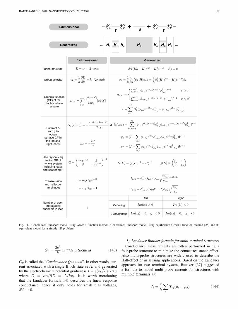
HATEF SADEGHI, 2018, NANOTECHNOLOGY, 29, 373001 18
Fig. 11. Generalized transport model using Green’s function method. Generalized transport model using equilibrium Green’s function method [28] and itsequivalent model for a simple 1D problem.
G0 =2e2
h' 77.5 µ Siemens (143)
G0 is called the ”Conductance Quantum”. In other words, cur-rent associated with a single Bloch state vk/L and generatedby the electrochemical potential gradient is I = e(vk/L)D∆µwhere D = ∂n/∂E = L/hvk. It is worth mentioningthat the Landauer formula 141 describes the linear responseconductance, hence it only holds for small bias voltages,δV → 0.
1) Landauer-Buttiker formula for multi-terminal structuresConductance measurements are often performed using a
four-probe structure to minimize the contact resistance effect.Also multi-probe structures are widely used to describe theHall-effect or in sensing applications. Based on the Landauerapproach for two terminal system, Buttiker [37] suggesteda formula to model multi-probe currents for structures withmultiple terminals as:
Ii =e
h
∑j
Tij(µi − µj) (144)

HATEF SADEGHI, 2018, NANOTECHNOLOGY, 29, 373001 19
where Ii is current at ith terminal and Tij is the transmissionprobability from terminal j to i. In a multi-terminal system, itis convenient to assume one of the probes as reference voltageVref = 0 and write currents based on that. As an example, fora four probe structure, current in each probe can be writtenas:
Ii =2e2
h
(Niδij −
∑j=1,2,3,4 Tij
)Vi (145)
where Ni is number of open conduction channels in lead i. Inthe four probe structure, if probe 3 and 4 are the outer voltageprobes (I3 = I4 = 0) and probe 1 and 2 are the inner currentprobes, the four probe conductance is
Gfour−probe = (2e2/h)(V3 − V4)/I1 (146)
2) Equilibrium vs. non-equilibrium I-VThe Landauer formula only holds in the linear response
regime. A transmission coefficient T (E) of particle withenergy E from one electrode to the other is obtained in thesteady state condition where the junction is assumed to beclose to equilibrium (δV → 0). In this regime, transmissioncoefficient is assumed to be not voltage dependent and currentis calculated using equation 140.
However, if transmission coefficient changes by appliedbias voltage (the non-linear regime), bias voltage dependenttransmission coefficient T (E, Vb) should be calculated. Inorder to take the effect of electric field on T (E) into account,new Hamiltonian for a given field is calculated. This isobtained by calculating the potential profile applied to thejunction due to the given electric field (e.g. bias voltage) usingPoisson’s equation 52U = −ρ/ε where U is potential profiledue to charge distribution ρ and ε is permittivity which couldvary spatially [12–14]. In the non-equilibrium condition, theLandauer formula (equation 140) takes the form,
I(Vb, Vg) =
e
h
∫dE T (E, Vb, Vg)
(f(E +
eVb2
)− f(E − eVb2
)
)(147)
where Vb and Vg are bias and gate voltages, respectivelyand T (E, Vb, Vg) is transmission coefficient calculated at eachbias and gate voltages. It is worth mentioning that in someexperiments, the measured conductance G = I/Vb is noisy.Therefore, the differential conductance map Gdiff (Vb, Vg) =dI(Vb, Vg)/dVb is plotted. This could be calculated by dif-ferentiation of equation 147 with respect to the bias voltageVb.
D. Non-equilibrium Green’s function formalism
If ES|ψ〉 = H|ψ〉 describes the properties of the closedsystem H with non-orthogonal basis set S, then once itconnects to the outside world and becomes an open system(see figure 12), a modified Schrodinger equation in the non-equilibrium condition could be written [12–14]:
ES|ψ〉 = H|ψ〉+ Σ|ψ〉+ |s〉 (148)
where the terms Σ|ψ〉 and |s〉 describe the outflow and inflow(e.g. see equation 60), respectively arises from the boundaryconditions. Equation 148 could be rewritten as
Fig. 12. Non-equilibrium Green’s function (NEGF) equations. [12–14]
|ψ〉 = [GR]|s〉 (149)
where GR = [ES − H − Σ]−1 is retarded Green’s function(GA = [GR]†), Σ = Σ1 + Σ2 + Σ0 is sum of self-energiesdue to the electrodes Σ1, Σ2, and surroundings Σ0 such asdephasing contact or inelastic scattering e.g. electron-phononcoupling, emission and absorption. Dephasing contact termscould be described by the SCF method whereas for inelasticprocesses one needs to use for instance Fermi’s golden ruleto describe these self energies. There are a few proposals inthe literature to treat incoherent and inelastic processes [12–14, 38]. Buttiker [38] suggests to treat the inelastic and inco-herent scattering by introducing a new probe to the originalcoherent system. This could be seen as assigning new self-energies associated with any inelastic or incoherent processes.However, if the incoherent and inelastic effects are treatedby introducing an extra electrode, corresponding distributionfunction e.g. Fermi function for electrons is assigned which ingeneral may not be the case. More generally, any incoherenceand/or inelastic processes are introduced by appropriate selfenergies which not necessarily described by equivalent Fermifunctions in the contact.
For a normal, coherent elastic junction if H1,2 are thecoupling matrices between electrode 1 (2) and scatteringregion and g1,2 are the surface Green’s function of the elec-trodes, Σ1,2 = H†1,2g1,2H1,2. Furthermore, current could becalculated as
I1 =e
hTrace[−Γ1G
n + Σin1 A] (150)
where Γ1 = i(Σ1 − Σ†1) is the imaginary part of the self-energy, Gn is the density matrix,
∑in1 = s1s
†1/2π is related
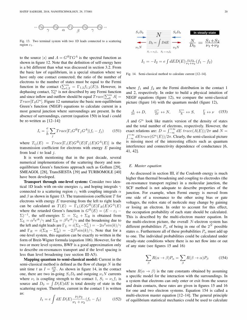
HATEF SADEGHI, 2018, NANOTECHNOLOGY, 29, 373001 20
Fig. 13. Two terminal system with two 1D leads connected to a scatteringregion ε1.
to the source |s〉 and A = GRΓGA is the spectral function asshown in figure 12. Note that the definition of self-energy hereis a bit different than what was discussed in section 3.2. Fromthe basic law of equilibrium, in a special situation where wehave only one contact connected; the ratio of the number ofelectrons to the number of states must be equal to the Fermifunction in the contact (
∑in1,2 = Γ1,2f1,2(E)). However, in
dephasing contact, Σin0 is not described by any Fermi functionand since inflow and outflow should be equal Trace[
∑in0 A] =
Trace[Γ0Gn]. Figure 12 summarize the basic non-equilibrium
Green’s function (NEGF) equations to calculate current in amost general junction where surroundings are present. In theabsence of surroundings, current (equation 150) in lead i couldbe re-written as [12–14]:
Ii =e
h
∑j
Trace[ΓiGRΓjG
A](fi − fj) (151)
where Tij(E) = Trace[Γi(E)GR(E)Γj(E)GA(E)] is thetransmission coefficient for electrons with energy E passingfrom lead i to lead j.
It is worth mentioning that in the past decade, severalnumerical implementations of the scattering theory and non-equilibrium Green’s functions approach such as Gollum [29],SMEAGOL [28], TransSIESTA [39] and TURBOMOLE [40]have been developed.
Transport through one-level system: Consider two iden-tical 1D leads with on-site energies ε0 and hoping integrals γconnected to a scattering region ε1 with coupling integrals αand β as shown in figure 13. The transmission coefficient T forelectrons with energy E traversing from the left to right leadscan be calculated as T (E) = ΓL(E)GR(E)ΓR(E)GA(E)where the retarded Green’s function is GR(E) = (E − ε1 −Σ)−1, the self-energies Σ = ΣL + ΣR is obtained fromΣL = α2eik/γ and ΣR = β2eik/γ and the broadening due tothe left and right leads are ΓL = i(ΣL−Σ†L) = −2α2sin(k)/γ
and ΓR = i(ΣR − Σ†R) = −2β2sin(k)/γ. Note that for aone-level system, this equation can be exactly re-written in theform of Breit-Wigner formula (equation 106). However, for thetwo or more level systems, BWF is a good approximation onlyto describe on-resonances transport and if the level spacing isless than level broadening (see section III-A5).
Mapping quantum to semi-classical model: Current in thesemi-classical method is defined as the flow of charge N in theunit time t as I = dN
dt . As shown in figure 14, in the contactone, there are two in-going S1D0 and outgoing ν1N currentswhere ν1 is coupling strength to the contact 1, S1 = ν1f1 issource and D0 =
∫D(E)dE is total density of state in the
scattering region. Therefore, current in the contact 1 is writtenas:
I1 = e
∫dE D(E)
ν1ν2
ν1 + ν2(f1 − f2) (152)
Fig. 14. Semi-classical method to calculate current [12–14].
where f1 and f2 are the Fermi distribution in the contact 1and 2, respectively. In order to build a physical intuition ofNEGF equations (figure 12), we compare the semi-classicalpicture (figure 14) with the quantum model (figure 12),
A2π ↔ D, Gn
2π ↔ N, Σin
~ ↔ S, Γ~ ↔ ν (153)
A and Gn look like matrix version of the density of statesand the total number of electrons, respectively. However, theexact relations are: D =
∫ +∞−∞ dE trace(A(E))/2π and N =∫ +∞
−∞ dEtrace(Gn(E))/2π. Clearly, the semi-classical pictureis missing most of the interesting effects such as quantuminterference and connectivity dependence of conductance [6,41, 42].
E. Master equation
As discussed in section III, if the Coulomb energy is muchhigher than thermal broadening and coupling to electrodes (theon-resonance transport regime) in a molecular junction, theSCF method is not adequate to describe properties of thejunction. For example, when Fermi energy is moved fromone side of a resonance to the other using bias or gatevoltages, the redox state of molecule may change by gainingor losing an electron. In order to account for this effect,the occupation probability of each state should be calculated.This is described by the multi-electron master equation. Inthe multi-electron picture, the overall N -electron system hasdifferent probabilities Pα of being in one of the 2N possiblestates α. Furthermore all of these probabilities Pα must add upto one. The individual probabilities could be calculated understeady-state conditions where there is no net flow into or outof any state (see figures 15 and 16)
∑β
R(α→ β)Pα =∑β
R(β → α)Pβ (154)
where R(α → β) is the rate constants obtained by assuminga specific model for the interaction with the surroundings. Ina system that electrons can only enter or exit from the sourceand drain contacts, these rates are given in figures 15 and 16for one and two electron systems. Equation 154 is called amulti-electron master equation [12–14]. The general principleof equilibrium statistical mechanics could be used to calculate

HATEF SADEGHI, 2018, NANOTECHNOLOGY, 29, 373001 21
the probability Pα that the system is in state α with energyEα and Nα electrons as
Pα =e−Eα−µNαkBT∑α e−Eα−µNαkBT
(155)
where kB is Boltzmann’s constant and T is temperature.One-electron energy levels represent differences between
energy levels corresponding to states that differ by one elec-tron. If E(N) is the energy associated with the N -electronstate, the energy associated with the addition of one electronis called affinity energy EA = E(N)− E(N + 1). Similarlythe energy needed to remove one electron is called ionizationenergy IP = E(N − 1)− E(N).
One electron system: Figure 15 shows the master equationfor spin-degenerate one electron system with energy ε wherethere are only two possibilities, either the state is full |1〉 orempty |0〉. Current is then calculated as:
I =e
~γ1γ2
γ1 + γ2(f1(E)− f2(E)) (156)
where γ1 and γ2 are the rates that electron can go in and outfrom the left and right electrodes with f1(E) and f2(E) Fermifunctions.
Two electron system: When the number of electrons Nincreases, the number of possibilities increases by 2N . In twoelectron system, there are four possibilities (22), both statesempty |00〉 or full |11〉 and either one of them full and theother empty (|01〉 and |10〉). Figure 16 shows how to calculatecurrent in two electron system [12–14]. Note that as soon as astate become full, there need an additional energy (Coulombrepulsion energy) to have second electron in the other state inaddition to the level spacing between the two energy levels.Furthermore, it is not correct to assume one Fermi function forall transitions. Due to the Coulomb blockade energy, each level
Fig. 15. Spin-degenerate one electron system with energy ε. There are twopossibilities either the state is full |1〉 or empty |0〉. The rate to move anelectron into the state (|0〉 to |1〉) is a product of the rates that electron cango in and the Fermi function in the leads (R(|0〉 → |1〉) = γ1f1 + γ2f2)[12–14]
Fig. 16. Two electron system. There are four possibilities, both states empty|00〉 or full |11〉 and either one of them full and the other empty (|01〉 and|10〉) [12–14].
needs certain electrochemical potential to overcome the barrierand current flow. Clearly, the expression for current in twoelectron system is more complicated than one electron system.This becomes even more complicated when multi-electronsystem was considered. In this case, the number of calculationsrapidly increases, therefore efficient numerical algorithms areneeded to solve the multi-electron master equation.
Coulomb and Franck-Condon blockade regimes: Theelectronic properties of weakly coupled molecules are domi-nated by Coulomb interactions and spatial confinement at lowtemperatures [43]. This could lead to Coulomb blockade (CB)regimes in which the transport is blocked due to the presenceof an electron trapped in the junction. In addition, chargetransfer can excite vibrational modes or vibrons, and strongelectron-vibron coupling leads to suppression of tunnel currentat low bias called Franck-Condon (FC) blockade regimes.
To describe transport in this regime, a minimal model(the Anderson-Holstein Hamiltonian) can be used [44] thatcaptures the CB, FC and the Kondo effect if three assumptionsare made: (1) the relaxation in the leads assumed to besufficiently fast leading to Fermi functions for the distributionof the electrons in thermal equilibrium at all times; (2) thetransport through the molecule is dominated by tunnellingthrough a single, spin-degenerate electronic level, and (3) onevibron taken into account within the harmonic approxima-tion. In this case, the Anderson-Holstein Hamiltonian readsH = Hmol +Hleads +HT with
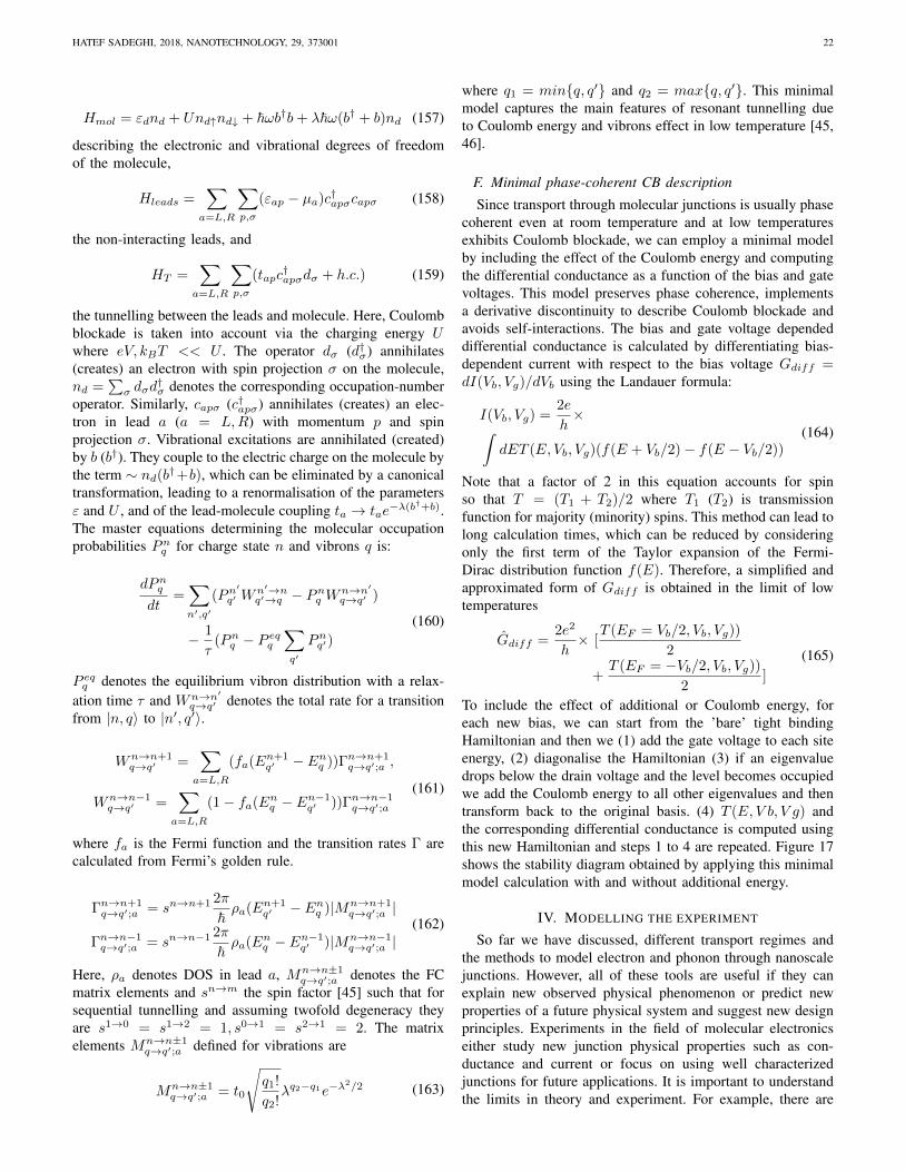
HATEF SADEGHI, 2018, NANOTECHNOLOGY, 29, 373001 22
Hmol = εdnd + Und↑nd↓ + ~ωb†b+ λ~ω(b† + b)nd (157)
describing the electronic and vibrational degrees of freedomof the molecule,
Hleads =∑a=L,R
∑p,σ
(εap − µa)c†apσcapσ (158)
the non-interacting leads, and
HT =∑a=L,R
∑p,σ
(tapc†apσdσ + h.c.) (159)
the tunnelling between the leads and molecule. Here, Coulombblockade is taken into account via the charging energy Uwhere eV, kBT << U . The operator dσ (d†σ) annihilates(creates) an electron with spin projection σ on the molecule,nd =
∑σ dσd
†σ denotes the corresponding occupation-number
operator. Similarly, capσ (c†apσ) annihilates (creates) an elec-tron in lead a (a = L,R) with momentum p and spinprojection σ. Vibrational excitations are annihilated (created)by b (b†). They couple to the electric charge on the molecule bythe term ∼ nd(b†+b), which can be eliminated by a canonicaltransformation, leading to a renormalisation of the parametersε and U , and of the lead-molecule coupling ta → tae
−λ(b†+b).The master equations determining the molecular occupationprobabilities Pnq for charge state n and vibrons q is:
dPnqdt
=∑n′,q′
(Pn′
q′ Wn′→nq′→q − Pnq Wn→n′
q→q′ )
− 1
τ(Pnq − P eqq
∑q′
Pnq′)
(160)
P eqq denotes the equilibrium vibron distribution with a relax-ation time τ and Wn→n′
q→q′ denotes the total rate for a transitionfrom |n, q〉 to |n′, q′〉.
Wn→n+1q→q′ =
∑a=L,R
(fa(En+1q′ − Enq ))Γn→n+1
q→q′;a ,
Wn→n−1q→q′ =
∑a=L,R
(1− fa(Enq − En−1q′ ))Γn→n−1
q→q′;a
(161)
where fa is the Fermi function and the transition rates Γ arecalculated from Fermi’s golden rule.
Γn→n+1q→q′;a = sn→n+1 2π
~ρa(En+1
q′ − Enq )|Mn→n+1q→q′;a |
Γn→n−1q→q′;a = sn→n−1 2π
~ρa(Enq − En−1
q′ )|Mn→n−1q→q′;a |
(162)
Here, ρa denotes DOS in lead a, Mn→n±1q→q′;a denotes the FC
matrix elements and sn→m the spin factor [45] such that forsequential tunnelling and assuming twofold degeneracy theyare s1→0 = s1→2 = 1, s0→1 = s2→1 = 2. The matrixelements Mn→n±1
q→q′;a defined for vibrations are
Mn→n±1q→q′;a = t0
√q1!
q2!λq2−q1e−λ
2/2 (163)
where q1 = minq, q′ and q2 = maxq, q′. This minimalmodel captures the main features of resonant tunnelling dueto Coulomb energy and vibrons effect in low temperature [45,46].
F. Minimal phase-coherent CB description
Since transport through molecular junctions is usually phasecoherent even at room temperature and at low temperaturesexhibits Coulomb blockade, we can employ a minimal modelby including the effect of the Coulomb energy and computingthe differential conductance as a function of the bias and gatevoltages. This model preserves phase coherence, implementsa derivative discontinuity to describe Coulomb blockade andavoids self-interactions. The bias and gate voltage dependeddifferential conductance is calculated by differentiating bias-dependent current with respect to the bias voltage Gdiff =dI(Vb, Vg)/dVb using the Landauer formula:
I(Vb, Vg) =2e
h×∫
dET (E, Vb, Vg)(f(E + Vb/2)− f(E − Vb/2))(164)
Note that a factor of 2 in this equation accounts for spinso that T = (T1 + T2)/2 where T1 (T2) is transmissionfunction for majority (minority) spins. This method can lead tolong calculation times, which can be reduced by consideringonly the first term of the Taylor expansion of the Fermi-Dirac distribution function f(E). Therefore, a simplified andapproximated form of Gdiff is obtained in the limit of lowtemperatures
Gdiff =2e2
h× [
T (EF = Vb/2, Vb, Vg))
2
+T (EF = −Vb/2, Vb, Vg))
2]
(165)
To include the effect of additional or Coulomb energy, foreach new bias, we can start from the ’bare’ tight bindingHamiltonian and then we (1) add the gate voltage to each siteenergy, (2) diagonalise the Hamiltonian (3) if an eigenvaluedrops below the drain voltage and the level becomes occupiedwe add the Coulomb energy to all other eigenvalues and thentransform back to the original basis. (4) T (E, V b, V g) andthe corresponding differential conductance is computed usingthis new Hamiltonian and steps 1 to 4 are repeated. Figure 17shows the stability diagram obtained by applying this minimalmodel calculation with and without additional energy.
IV. MODELLING THE EXPERIMENT
So far we have discussed, different transport regimes andthe methods to model electron and phonon through nanoscalejunctions. However, all of these tools are useful if they canexplain new observed physical phenomenon or predict newproperties of a future physical system and suggest new designprinciples. Experiments in the field of molecular electronicseither study new junction physical properties such as con-ductance and current or focus on using well characterizedjunctions for future applications. It is important to understandthe limits in theory and experiment. For example, there are

HATEF SADEGHI, 2018, NANOTECHNOLOGY, 29, 373001 23
Fig. 17. Stability diagram.(a) a tight-binding model consists of two one-dimensional leads with hopping elements of γ = −2 (which sets the energyscale) connected to a scattering region containing 10 sites with hoppingelements γi = −[0.25, 0.125, 0.25, 0.25, 0.075, 0.2, 0.2, 0.25, 0.25, 0.4].All on site energies (εi and ε0) are set to zero. The scattering region iscoupled to the left and right electrodes by hopping elements α = 0.1γ. (b,d)The differential conductance dI(Vb = 0, Vg)/dVb. (c,e) The stability diagramdI(Vb, Vg)/dVb is obtained by applying minimal model calculation (sectionIII-F). In c,d the the Coulomb energy U is zero whereas in e,f U = 0.125γ.Chessboard pattern due to quantum interference is obtained in c. By includingadditional energy U , the size of Coulomb diamonds (blockade region) isincreased accordingly and excited states do not penetrate to the blockaderegion.
certain quantities that are not directly measurable but canbe calculated such as wave-functions. In contrast, there arequantities that are not predictable but accessible in experimentsuch as the position of the Fermi energy, the overall effect ofthe inhomogeneous broadening on the transport, or screeningeffects which is related to the exact junction configuration inthe real-time experiment.
Furthermore, more reliable predictions can be made ifa series of junctions were studied and the overall trendscompared between theory and experiment. The bottom line istheory and experiment are not two isolated endeavours. Theyneed to communicate with each other in order to discover newphenomena. Those quantities that cannot be computed reliably,but for which experimental data is available, can be used tocorrect and refine theoretical models. Usually to explain newphenomena, one needs to build a model based on a workinghypothesis. To make an initial hypothesis, a theorist needs toknow how to take into account different physical phenomenasuch as the effect of environment, presence of an electric or
magnetic field. In the following, the aim is to make few bridgesbetween the well-known physical phenomena and the methodsto model them theoretically.
A. Virtual leads versus physical leads
Let’s start by considering the differences between a lead anda channel. From a mathematical viewpoint, channels connectan extended scattering region to a reservoir and the role of leadi is simply to label those channels ki, qi, which connect to aparticular reservoir i. Conceptually, this means that from thepoint of view of solving a scattering problem at energy E, asingle lead with N(E) incoming channels can be regarded asN(E) virtual leads, each with a single channel. We could takeadvantage of this equivalence by regarding the above groupsof channels with wave-vectors kαi , qαi as virtual leads andtreating them on the same footing as physical leads [29].
This viewpoint is particularly useful when the HamiltoniansHi
0, Hi1 describing the principle layers PLs (the identical
periodic unit cells Hi0 connected to each other by Hi
1) of thephysical lead i are block diagonal with respect to the quantumnumbers associated with kαi , qαi . For example, this occurswhen the leads possess a uniform magnetization, in whichcase the lead Hamiltonian is block diagonal with respect tothe local magnetization axis of the lead and α represents thespin degree of freedom σ. This occurs also when the leads arenormal metals, but the scattering region contains one or moresuperconductors, in which case the lead Hamiltonian is blockdiagonal with respect to particle and hole degrees of freedomand α represents either particles p or holes h. More generally,in the presence of both magnetism and superconductivity, αwould represent combinations of spin and particles and holesdegrees of freedom.
In all of these cases, Hi0, Hi
1 are block diagonal and itis convenient to identify virtual leads αi with each block,because we can compute the channels kαi , qαi belonging toeach block in separate calculations and therefore guaranteesthat all such channels can be separately identified. This isadvantageous, because if all channels of Hi
0, Hi1 were calcu-
lated simultaneously, then in the case of degeneracies, arbitrarysuperposition of channels with different quantum numberscould result and therefore it would be necessary to implement aseparate unitary transformation to sort channels into the chosenquantum numbers. By treating each block as a virtual lead, thisproblem is avoided.
B. Charge, spin and thermal currents
When comparing theory with experiment, we are usuallyinterested in computing the flux of some quantity Q froma particular reservoir. If the amount of Q carried by quasi-particles of type αi is Qαi(E), then the flux of Q fromreservoir i is:
IiQ =1
h
∫dE
∑αi,j,βj
T i,jαi,βj fjβj
(E) (166)
T i,jαi,βj in this expression is transmission coefficient of quasi-particles of type αi. In the simplest case of a normal conductor,
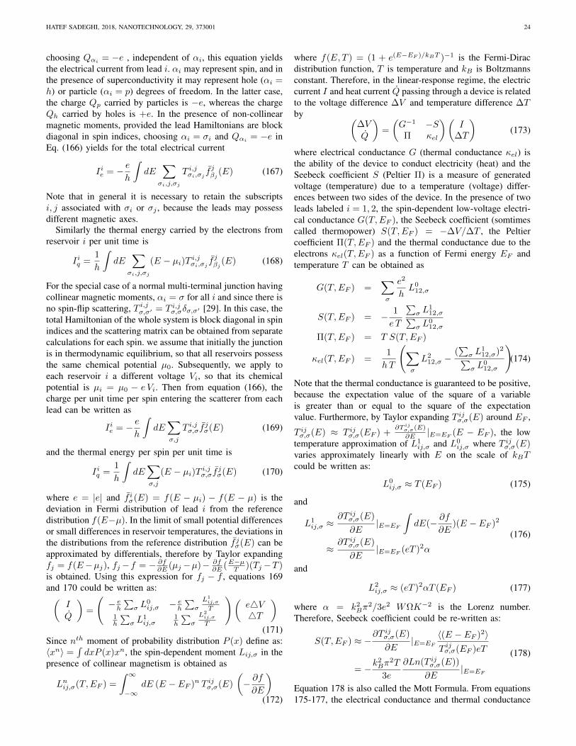
HATEF SADEGHI, 2018, NANOTECHNOLOGY, 29, 373001 24
choosing Qαi = −e , independent of αi, this equation yieldsthe electrical current from lead i. αi may represent spin, and inthe presence of superconductivity it may represent hole (αi =h) or particle (αi = p) degrees of freedom. In the latter case,the charge Qp carried by particles is −e, whereas the chargeQh carried by holes is +e. In the presence of non-collinearmagnetic moments, provided the lead Hamiltonians are blockdiagonal in spin indices, choosing αi = σi and Qαi = −e inEq. (166) yields for the total electrical current
Iie = − eh
∫dE
∑σi,j,σj
T i,jσi,σj fjβj
(E) (167)
Note that in general it is necessary to retain the subscriptsi, j associated with σi or σj , because the leads may possessdifferent magnetic axes.
Similarly the thermal energy carried by the electrons fromreservoir i per unit time is
Iiq =1
h
∫dE
∑σi,j,σj
(E − µi)T i,jσi,σj fjβj
(E) (168)
For the special case of a normal multi-terminal junction havingcollinear magnetic moments, αi = σ for all i and since there isno spin-flip scattering, T i,jσ,σ′ = T i,jσ,σδσ,σ′ [29]. In this case, thetotal Hamiltonian of the whole system is block diagonal in spinindices and the scattering matrix can be obtained from separatecalculations for each spin. we assume that initially the junctionis in thermodynamic equilibrium, so that all reservoirs possessthe same chemical potential µ0. Subsequently, we apply toeach reservoir i a different voltage Vi, so that its chemicalpotential is µi = µ0 − e Vi. Then from equation (166), thecharge per unit time per spin entering the scatterer from eachlead can be written as
Iie = − eh
∫dE∑σ,j
T i,jσ,σ fjσ(E) (169)
and the thermal energy per spin per unit time is
Iiq =1
h
∫dE∑σ,j
(E − µi)T i,jσ,σ f jσ(E) (170)
where e = |e| and f iσ(E) = f(E − µi) − f(E − µ) is thedeviation in Fermi distribution of lead i from the referencedistribution f(E−µ). In the limit of small potential differencesor small differences in reservoir temperatures, the deviations inthe distributions from the reference distribution f jσ(E) can beapproximated by differentials, therefore by Taylor expandingfj = f(E−µj), fj−f = − ∂f
∂E (µj−µ)− ∂f∂E (E−µT )(Tj−T )
is obtained. Using this expression for fj − f , equations 169and 170 could be written as:(
I
Q
)=
(− eh
∑σ L
0ij,σ − e
h
∑σ
L1ij,σ
T
1h
∑σ L
1ij,σ
1h
∑σ
L2ij,σ
T
)(e4V4T
)(171)
Since nth moment of probability distribution P (x) define as:〈xn〉 =
∫dxP (x)xn, the spin-dependent moment Lij,σ in the
presence of collinear magnetism is obtained as
Lnij,σ(T,EF ) =
∫ ∞−∞
dE (E − EF )n T ijσ,σ(E)
(− ∂f∂E
)(172)
where f(E, T ) = (1 + e(E−EF )/kBT )−1 is the Fermi-Diracdistribution function, T is temperature and kB is Boltzmannsconstant. Therefore, in the linear-response regime, the electriccurrent I and heat current Q passing through a device is relatedto the voltage difference ∆V and temperature difference ∆Tby (
∆V
Q
)=
(G−1 −SΠ κel
)(I
∆T
)(173)
where electrical conductance G (thermal conductance κel) isthe ability of the device to conduct electricity (heat) and theSeebeck coefficient S (Peltier Π) is a measure of generatedvoltage (temperature) due to a temperature (voltage) differ-ences between two sides of the device. In the presence of twoleads labeled i = 1, 2, the spin-dependent low-voltage electri-cal conductance G(T,EF ), the Seebeck coefficient (somtimescalled thermopower) S(T,EF ) = −∆V/∆T , the Peltiercoefficient Π(T,EF ) and the thermal conductance due to theelectrons κel(T,EF ) as a function of Fermi energy EF andtemperature T can be obtained as
G(T,EF ) =∑σ
e2
hL0
12,σ
S(T,EF ) = − 1
e T
∑σ L
112,σ∑
σ L012,σ
Π(T,EF ) = T S(T,EF )
κel(T,EF ) =1
hT
(∑σ
L212,σ −
(∑σ L
112,σ)2∑
σ L012,σ
)(174)
Note that the thermal conductance is guaranteed to be positive,because the expectation value of the square of a variableis greater than or equal to the square of the expectationvalue. Furthermore, by Taylor expanding T ijσ,σ(E) around EF ,
T ijσ,σ(E) ≈ T ijσ,σ(EF ) +∂T ijσ,σ(E)
∂E |E=EF (E − EF ), the lowtemperature approximation of L1
ij,σ and L0ij,σ where T ijσ,σ(E)
varies approximately linearly with E on the scale of kBTcould be written as:
L0ij,σ ≈ T (EF ) (175)
and
L1ij,σ ≈
∂T ijσ,σ(E)
∂E|E=EF
∫dE(− ∂f
∂E)(E − EF )2
≈∂T ijσ,σ(E)
∂E|E=EF (eT )2α
(176)
and
L2ij,σ ≈ (eT )2αT (EF ) (177)
where α = k2Bπ
2/3e2 WΩK−2 is the Lorenz number.Therefore, Seebeck coefficient could be re-written as:
S(T,EF ) ≈ −∂T ijσ,σ(E)
∂E|E=EF
〈(E − EF )2〉T ijσ,σ(EF )eT
= −k2Bπ
2T
3e
∂Ln(T ijσ,σ(E))
∂E|E=EF
(178)
Equation 178 is also called the Mott Formula. From equations175-177, the electrical conductance and thermal conductance
HATEF SADEGHI, 2018, NANOTECHNOLOGY, 29, 373001 25
due to electrons are obtained as G(T,EF ) ≈ G0T (EF ) andκel(T,EF ) ≈ αTG(T,EF ). The latter is also called theWiedemann-Franz law and shows that thermal conductancedue to electrons is proportional to the electrical conductance.
Efficiency of a thermoelectric martial η is defined as theratio between the work done per unit time against the chemicalpotential difference (between two hot and cold reservoir) andthe heat extracted from the hot reservoir per unit time. Themaximum efficiency ηmax could be written as:
ηmax =∆T
Th
√Z.Tavg + 1− 1√Z.Tavg + 1 + Tc
Th
(179)
where Th and Tc are temperatures of hot- and cold-sides,respectively, ∆T = Th − Tc and Tavg = (Th + Tc)/2.The thermoelectric conversion efficiency (equation 179) is theproduct of the Carnot efficiency ( ∆T
Th) and a reduction factor as
a function of the material’s figure of merit Z = S2G/κ, whereS, G, and κ = κel+κph are the Seebeck coefficient, electricalconductance, and thermal conductance due to both electronsand phonons, respectively. More commonly a dimensionlessfigure of merit (ZT = Z.Tavg) is used to account for theefficiency of the thermoelectric materials. The thermoelectricfigure of merit could be written as
ZT = ZTelκel
κel + κph(180)
where the electronic thermoelectric figure of merit for a two-terminal system is
ZTel =L1
12
L012 L
212 − L1
12
(181)
To calculate the total ZT , not only the thermal conductancedue to the electrons are needed but also it is absolutely crucialto take the phonons contribution to the thermal conductance(κph) into account as described in the next section.
C. Phonon thermal conductance
To calculate the heat flux through a molecular junctioncarried by the phonons, equation 166 could be used wherethe thermal conductance due to the phonons κph could beobtained [10] by calculating the phononic transmission Tphfor different vibrational modes as
κph(T ) =1
2π
∫ ∞0
~ωTph(ω)∂fBE(ω, T )
∂Tdω (182)
where fBE(ω, T ) = (e~ω/kBT − 1)−1 is Bose-Einstein dis-tribution function and ~ is reduced Plancks constant and kBis Boltzmanns constant. To calculate the vibrational modesof a system, we use the harmonic approximation method toconstruct the dynamical matrix D. From the ground staterelaxed xyz coordinate of the system, each atom is displacedfrom its equilibrium position by δq′ and −δq′ in x, y andz directions and the forces F qi = (F xi , F
yi , F
zi ) in three
directions qi = (xi, yi, zi) on each atom are calculated. For3n degrees of freedom (n = number of atoms), the 3n × 3ndynamical matrix D is constructed from Hessian matrix K
Dij =Kqq′
ij
Mij(183)
where Kqq′
ij for i 6= j are obtained from finite differences
Kqq′
ij =F qi (δq′j)− F
qi (−δq′j)
2δq′j(184)
and the mass matrix M =√MiMj . To satisfy momentum
conservation, the Ks for i = j (diagonal terms) are calculatedfrom Kii = −
∑i 6=j Kij . Once the dynamical matrix is con-
structed the Green’s function method as described in sectionIII-B could be used to calculate the phononic transmissioncoefficient Tph.
It is worth to mention that in order to compute the electron-phonon coupling matrices Wλ for a given phononic mode λ,one could use the Hamiltonian matrices 〈i|H|j〉 for thedisplaced configurations [47].
〈i| ∂H∂δq′|j〉 =
∂〈i|H|j〉∂δq′
− ∂〈i|∂δq′|H|j〉 − 〈i|H| ∂|j〉
∂δq′(185)
where |i〉 are basis orbitals. The Wλ matrices are then used[47] to calculate the appropriate self-energies (see sectionIII-D) to account for inelastic scattering due to electron-phonon interactions.
D. Piezoelectric response
In piezoelectric materials, electric field is generated due toconformational changes. The piezoelectric response betweenatoms i and j of a molecule is given by:
Pij =
∂u∂fj− ∂u
∂fi
rij(186)
where rij is the distance between atom i and j in theequilibrium geometry. Displacement derivatives ∂u
∂f is givenby
∂u
∂f= −VW−1H (187)
where W and V are normal modes and vectors of Hessianmatrix K = ∂2E
∂u2 , respectively (section IV-C). H = V TH
where H = ∂2E∂f∂u is dipole derivatives matrix. Note that just
like equation 184, these derivatives can be calculated usingfinite differences. Clearly, larger piezoelectric response isexpected for molecules with larger dipole moments. Recently,a large converse piezoelectric effect was measured in helicenesingle molecules [48].
E. Spectral adjustment
Although DFT has been successful at predicting the trends,it usually underestimates the position of the Fermi energyEF , the exact energy levels (Kohn-Sham eigenvalues [49])and therefore the position of the HOMO and LUMO and theenergy gap. To compare mean-field theory with experiment,some corrections are needed. One way is to use hybrid func-tionals e.g. B3LYP [50] or many body calculations e.g. GW
HATEF SADEGHI, 2018, NANOTECHNOLOGY, 29, 373001 26
approximation [51]. The latter is computationally expensive[52] and can only be used for molecules with few atoms. Analternative way is to correct the HOMO-LUMO gap using thevalues measured experimentally. A phenomenological schemethat improves the agreement between theoretical simulationsand experiments in, for example, single-molecule electronicsconsists of shifting the occupied and unoccupied levels ofthe molecule (M) downwards and upwards, respectively toincrease the energy gap. The procedure is conveniently calledspectral adjustment in nanoscale transport [29, 53] and hasbeen widely used in the literature to correct theoretical trans-port gap [54, 55]. The Hamiltonian K = H −ES of a givenM region could be modified as:
KM = K0M + (∆o −∆u)SM ρM SM + ∆u SM (188)
where ∆o,u are energy shifts. ρM =∑no |Ψno〉〈Ψno| is
the density matrix where (no, nu) denote the occupied andunoccupied states, respectively and SM is overlap matrix. Ifexperimental HOMO and LUMO energies are available, ∆o,u
can be chosen to correct HOMO and LUMO obtained from themean-field Hamiltonian. Alternatively, in the simplest case, theshifts ∆o,u are chosen to align the highest occupied and lowestunoccupied molecular orbitals (ie the HOMO and LUMO)with (minus) the ionization potential (IP ) and electron affinity(EA) of the gas phase molecule
∆0o = εHOMO + IP + Z
∆0u = −εLUMO − EA− Z
(189)
The ionization potential (IP = E(+e) − E(0)) and electronaffinity (EA = E(0) − E(−e)) are calculated from totalenergy calculation of the gas phase molecule. E(0) is the totalenergy of the neutral molecule, E(+e) is the energy of themolecule with one electron removed (i.e. positively charged),and E(−e) is the total energy of the molecule with one addedelectron. The energy-gap Eg of a molecule (sometimes calledadditional energy) could be calculated from IP and EA as:Eg = IP − EA [12–14]. The important conceptual point isthat the electrochemical potential µ should lie between theaffinity levels (above µ) and ionization levels (below µ) in theground state. Note that IP and EA are traditionally definedpositive energies below the vacuum level, whereas HOMO andLUMO level are negative, if they are below the vacuum level.
The Coulomb interactions in the isolated molecule arescreened if it is placed in close proximity to a metallic surface.Due to this image charge interactions, the occupied energylevels shift up whereas the unoccupied states move downresulting in shrinking of energy gap. This could be taken intoaccount by using a simple image charge model, where themolecule is replaced by a point charge located at the middlepoint of the molecule and where the image planes are placed∼ 1 A above the electrodes’ surfaces. Then the shifts arecorrected by screening effects Z = e2 ln 2/(8πε0a) where ais the distance between the image plane and the point imagecharge.
F. Hopping versus tunnelling
Charge transport mechanism through the molecular scalejunctions are either coherent transport via tunnelling (calledalso superexchange) or incoherent thermally activated hop-ping. Transport through the short molecules with the lengthof < 3− 4nm has been demonstrated [56, 57] to be coherenttunnelling. This is characterized by an exponential dependenceof conductance G with length given by
G = Gce−βL (190)
where Gc is a pre-exponential factor dependent on junctioncontacts and nature of metallic leads, β is the tunnelling decayconstant (called also attenuation or β factor), and L is thelength of the molecule. The coherent process is also character-ized by temperature independence. In contrast, incoherent hop-ping is believed to be the charge transport mechanism alonglonger molecules. In incoherent hopping transport regime, theconductance follows an Arrhenius relation
G = Gae−EA/kBT (191)
where Ga is a constant pre-exponential factor for each chem-ical reaction, EA is the hopping activation energy, T is thetemperature and kB is the Boltzmann’s constant. In thisregime, the conductance varies as the inverse of molecu-lar length and also decays exponentially with temperature.Therefore, the length and temperature dependent conductancemeasurements are widely used in the literature to distinguishbetween different transport regimes [58, 59].
G. Spin Hamiltonian
To take electrons spin into account in a Hamiltonian H(Eψ = Hψ), in the absence of spin-orbit coupling, theSchrodinger equation can be written,
E
(ψ
ψ
)=
(H 00 H
)(ψ
ψ
)(192)
where ψ and ψ are spin-up and spin-down component of wave-function. If electrons travel with high velocities, relativisticeffects can become significant. This is not usually a case insolids but near the nuclei of atoms where the electric fields arehigh, weak relativistic effects might be expected. Therefore,a spin-orbit correction need to be considered using the Diracequation.
E
(ψ
ψ
)=
(H 00 H
)(ψ
ψ
)+
(Mz Mx − iMy
Mx + iMy −Mz
)(ψ
ψ
) (193)
Spin-orbit Hamiltonian is often written as σ.M where σ isPauli spin matrices.
σx =
(0 11 0
), σy =
(0 −ii 0
), σz =
(1 00 −1
)(194)
If M points in the direction (θ, φ), Mx = sin θ cos φ, My =sin θ sin φ and Mz = cos θ, therefore

HATEF SADEGHI, 2018, NANOTECHNOLOGY, 29, 373001 27
Fig. 18. Magnetisim. Schematic represents a scattering region with two 1D chain for each spin. ε1 and ε2 are site energies for spin-up and spin-down,respectively. In the para-magnetic case, the site energies for spin-up and spin-down are equal ε0. In the presence of spin-orbit coupling, there are couplingbetween spin-up and spin-down sites.
(Mz Mx − iMy
Mx + iMy −Mz
)=
(cos θ sin θ e−iφ
sin θ eiφ −cos θ
)(195)
The spin wavefunction, spinors thus is obtainedψ =
(cos(θ/2) e−iφ/2
sin(θ/2) eiφ/2
), ψ =
(−sin(θ/2) e−iφ/2
cos(θ/2) eiφ/2
). If there
is no spin-orbit coupling, the Hamiltonian is block diagonalfor spin up and spin down. Therefore, transmission coefficientfor spin up and down could be treated independently. Ifan scattering region cause spin flip, the new Hamiltonianis twice bigger than Hamiltonian without spin and tocalculate transmission coefficient, one need to consider wholeHamiltonian. For a para-magnetic system, one could obtainthe total transmission by multiplying one spin transmissionby 2. Figure 18 shows examples of ferromagnetic andanti-ferromagnetic systems.
H. Inclusion of a Gauge field
For a scattering region of area A, if a magnetic fieldB is applied the magnetic flux φ = B × A. To computetransport properties in the presence of a magnetic field, aPeierls substitution is considered by changing the phase factorsof the coupling elements between atomic orbitals. For examplein the case of a nearest-neighbor tight-binding Hamiltonian,the hoping matrix element Hij between site i and site j isreplaced with the modified element,
HBij = Hije
−iφ, (196)
where
φ =e
~
∫ ri
rj
A(r)dr (197)
and ri and rj are the positions of site i and j and A is thevector potential. The gauge should be chosen such that theprincipal layers of the leads remain translationally invariantafter the substitution.
I. Superconducting systems
Figure 19a shows a two-probe normal-superconductor-normal device with left and right normal reservoirs connectedto a scattering region containing one or more superconductors.If the complete Hamiltonian describing a normal system isHN , then in the presence of superconductivity within theextended scattering region, the new system is described bythe Bogoliubov-de Gennes Hamiltonian
H =
(HN ∆∆∗ −H∗N
)(198)
Virtual Leadelectrons
Virtual Leadholes
Fig. 19. Two-terminal device consists of two physical leads connected to ascattering region containing two superconductors with order parameters 41
and 42. The left (right) physical lead consists of two virtual leads p1 andh1 (p2 and h2) carrying particle and hole channels, respectively.
where the elements of the matrix ∆ are non-zero only in theregion occupied by a superconductor, as indicated in figure19b. Physically, HN describes particle degrees of freedom,−H∗N describes hole degrees of freedom and ∆ is the super-conducting order parameter.
The multi-channel scattering theory for such a normal-superconducting-normal structure could be written as [29]:(
ILIR
)=
2 e2
ha
(µL−µe
µR−µe
)(199)
where IL (IR) is the current from the left (right) reservoir,µL − µ (µR − µ) is the difference between the chemicalpotential of the left (right) reservoir and the chemical potentialµ of the superconducting condensate and the voltage differencebetween the left and right reservoirs is (µL − µR)/e. In thisequation,
a =
(NL −Ro +Ra −T ′o + T ′a−To + Ta NR −R′o +R′a
)(200)
where NL (NR) is the number of open channels in the left(right) lead, Ro, To (Ra, Ta) are normal (Andreev) reflectionand transmission coefficients for quasi-particles emitted fromthe right lead, R′o, T
′o (R′a, T
′a) are normal (Andreev) reflec-
tion and transmission coefficients from the left lead and allquantities are evaluated at the Fermi energy E = µ. As aconsequence of unitarity of the scattering matrix, these satisfyRo + To +Ra + Ta = NL and R′o + T ′o +R′a + T ′a = NR.
The current-voltage relation of equation 199 is fundamen-tally different from that encountered for normal systems,because unitarity of the s-matrix does not imply that the sumof each row or column of the matrix a is zero. Consequently,the currents do not automatically depend solely on the appliedvoltage difference (µL − µR)/e (or more generally on thedifferences between incoming quasi-particle distributions). Inpractice such a dependence arises only after the chemicalpotential of the superconductor adjusts itself self-consistentlyto ensure that the current from the left reservoir is equal to thecurrent entering the right reservoir. Insisting that IL = −IR =

HATEF SADEGHI, 2018, NANOTECHNOLOGY, 29, 373001 28
I , the two-probe conductance G = I/((µL−µR)/e) takes theform of
G =2 e2
h
a11a22 − a12a21
a11 + a22 + a12 + a21(201)
If a superconductor is disordered, then as its length L in-creases, all transmission coefficients vanish. Consequently, thesuperconductor possesses zero resistivity (equation 201). Inthis limit, the above equation reduces to (h/2e2)G = 2/Ra +2/R′a. In contrast with a normal scatterer, this shows that inthe presence of Andreev scattering, as L tends to infinity, theresistance ( = 1/conductance) remains finite and therefore theresistivity (i.e. resistance per unit length) vanishes.
J. Environmental effects
Environmental effects such as presence of water, counter-ions, solvents, pH, molecules conformational change, dopants,nearby molecules, charge trap in a substrate can affect trans-port properties through a molecular junction. In order to modelthese effects, a statistical analysis needs to be carried out.Since a molecular junction in the presence of surroundingmolecules is a dynamic object at room temperature, a molec-ular dynamics simulation is usually needed to understand therange of possible configurations of the system. A few con-figuration then should be extracted and full DFT calculationscarried out to obtain the mean field Hamiltonian of the systemin the presence of surrounding molecules. An alternativeway to study the environmental effect is to create a seriesof more ideal configurations systematically in the presenceof surrounding molecules (e.g. by moving surroundings indifferent directions). Then without geometry optimization, onecould calculate the binding energy of surroundings to themolecule for each configuration and study transport propertiesof the confirmations with higher binding energies. Alterna-tively, Boltzmann distribution Tnew = Told × e|E
binding|/kBT
can be used to account for the weight of each confirmation ontotal ensemble transmission coefficient. Both of these methodsare widely used in the literature to model environmentaleffects.
To calculate the binding energy between surroundings Sand the backbone B, three total energy calculations need to becarried out. (1) The total energy of whole structure includingsurroundings and the backbone ESB , (2) The total energy ofthe surroundings in the presence of the backbone ghost statesESb, (3) The total energy of backbone in the presence of thesurroundings ghost states EsB . The binding energy is thenobtained by EbindingSB = ESB − (ESb + EsB). It is worthmentioning that since different effects such as physobrtion andcharge transfer can play important role in these simulations,SCF methods need to be used to calculate transport from themean-field DFT Hamiltonian. Recently, machine learning al-gorithms have been proposed to predict behavior of a junctionin the absence/presence of surroundings. In these methods,machine is trained using a series of molecular junctions whichare fully characterised using SCF methods. Machine thenpredicts the behavior of new junctions using its data base andpattern recognition algorithms.
V. CONCLUSION
To understand, predict and explain new phenomenon inthe nanoscale junctions, one needs to study electron, phononand spin transport through these junctions. The focus of thispaper was on exploring theoretical methods to study electron,phonon and spin transports through molecules and low di-mensional materials. Systematic study of such systems beginswith understanding their vibrational and electronic structure.Then, one need to calculate the core quantities, transmissionfunction of electrons Te and phonons Tph traversing throughsuch systems from one electrode to the other. This is not onlyvital to understand their properties and related experimentsbut also to develop new concepts and design strategies forfuture applications. We mainly considered junctions where thetransport is assumed to be elastic and coherent. In addition, weshowed that how these methods could be extended to the inco-herent and inelastic regimes. A good agreement between ex-periments and theories devolved using these methods [6, 9, 11]demonstrate that they are accurate enough to predict trends anddevelop new design strategies for future applications. However,in terms of predicting actual numbers, there are rooms forimprovements. Apart from those quantities that depends on theactual shape of the contact (e.g. screening effects) and cannotbe easily calculated; new computationally cheap approachesare needed to take into account electron-electron interactionsmore accurately. This would help to predict more accurateenergy gap and level spacing leading to more realistic modells.
ACKNOWLEDGEMENT
H.S. acknowledges the Leverhulme Trust for LeverhulmeEarly Career Fellowship no. ECF-2017-186.
REFERENCES
[1] “Itrs roadmap 2015,” ITRS, 2015.[2] M. Chhowalla, D. Jena, and H. Zhang, “Two-dimensional
semiconductors for transistors,” Nat. Rev. Mater., vol. 1, no. 11,p. 16052, 2016.
[3] “Visions for a molecular future,” Nature Nanotechnology, vol. 8,no. 6, pp. 385–389, 2013.
[4] J. L. Christopher, L. A. Estroff, J. K. Kriebel, R. G. Nuzzo,and G. M. Whitesides, “Self-assembled monolayers of thiolateson metals as a form of nanotechnology,” Chemical Reviews,vol. 105, no. 4, pp. 1103–1170, 2005. PMID: 15826011.
[5] S. V. Aradhya and L. Venkataraman, “Single-molecule junctionsbeyond electronic transport,” Nature Nanotechnology, vol. 8,no. 6, pp. 399–410, 2013.
[6] S. Sangtarash, C. Huang, H. Sadeghi, G. Sorohhov, J. Hauser,T. Wandlowski, W. Hong, S. Decurtins, S.-X. Liu, and C. J.Lambert, “Searching the Hearts of Graphene-like Moleculesfor Simplicity, Sensitivity, and Logic,” Journal of the AmericanChemical Society, vol. 137, no. 35, pp. 11425–11431, 2015.
[7] H. Sadeghi, L. Algaragholy, T. Pope, S. Bailey, D. Visontai,D. Manrique, J. Ferrer, V. Garcia-Suarez, S. Sangtarash, andC. J. Lambert, “Graphene sculpturene nanopores for DNAnucleobase sensing,” Journal of Physical Chemistry B, vol. 118,no. 24, pp. 6908–6914, 2014.
[8] T. Prodromakis, C. Toumazou, and L. Chua, “Two centuriesof memristors,” Nature Materials, vol. 11, no. 6, pp. 478–481,2012.
[9] H. Sadeghi, J. A. Mol, C. S. Lau, G. A. D. Briggs, J. Warner,and C. J. Lambert, “Conductance enlargement in picoscale elec-troburnt graphene nanojunctions,” Proceedings of the NationalAcademy of Sciences, vol. 112, no. 9, pp. 2658–2663, 2015.
HATEF SADEGHI, 2018, NANOTECHNOLOGY, 29, 373001 29
[10] H. Sadeghi, S. Sangtarash, and C. J. Lambert, “Oligoyne molec-ular junctions for efficient room temperature thermoelectricpower generation,” Nano letters, vol. 15, no. 11, pp. 7467–7472,2015.
[11] C. Evangeli, K. Gillemot, E. Leary, M. T. Gonzalez, G. Rubio-Bollinger, C. J. Lambert, and N. Agraıt, “Engineering thethermopower of C60 molecular junctions,” Nano Lett., vol. 13,no. 5, pp. 2141–2145, 2013.
[12] S. Datta, Quantum Transport : Atom to Transistor. CambridgeUniv Pr, 2005.
[13] “nanohub-u: Fundamentals of nanoelectronics - part a.” https://nanohub.org/courses/fon1.
[14] “nanohub-u: Fundamentals of nanoelectronics - part b.” https://nanohub.org/courses/fon2.
[15] R. Gebauer and R. Car, “Kinetic theory of quantum transportat the nanoscale,” Phys. Rev. B, vol. 70, p. 125324, Sep 2004.
[16] M. Buttiker, “Scattering theory of current and intensity noisecorrelations in conductors and wave guides,” Phys. Rev. B,vol. 46, pp. 12485–12507, Nov 1992.
[17] E. Bonet, M. M. Deshmukh, and D. C. Ralph, “Solving rateequations for electron tunneling via discrete quantum states,”Phys. Rev. B, vol. 65, p. 045317, Jan 2002.
[18] E. Schrodinger, “An Undulatory Theory of the Mechanics ofAtoms and Molecules,” Phys. Rev., vol. 28, pp. 1049–1070, dec1926.
[19] E. Runge and E. K. U. Gross, “Density-functional theory fortime-dependent systems,” Phys. Rev. Lett., vol. 52, pp. 997–1000, Mar 1984.
[20] E. Engel and R. M. Dreizler, Density Functional Theory,vol. 2011. Springer Verlag, 2011.
[21] N. Harrison, “An introduction to density functional theory,”NATO Science Series Sub Series III: Computer and systemssciences, vol. 187, pp. 45–70, 2003.
[22] C. Lee, W. Yang, and R. G. Parr, “Development of the colle-salvetti correlation-energy formula into a functional of theelectron density,” Phys. Rev. B, vol. 37, pp. 785–789, Jan 1988.
[23] J. Heyd, G. E. Scuseria, and M. Ernzerhof, “Hybrid functionalsbased on a screened coulomb potential,” The Journal of Chem-ical Physics, vol. 118, no. 18, pp. 8207–8215, 2003.
[24] M. Dion, H. Rydberg, E. Schroder, D. C. Langreth, and B. I.Lundqvist, “Van der waals density functional for general ge-ometries,” Phys. Rev. Lett., vol. 92, p. 246401, Jun 2004.
[25] J. M. J. M. Soler, E. Artacho, J. D. Gale, A. Garcıa, J. Junquera,P. Ordejon, D. Sanchez-Portal, A. Garcia, J. Junquera, P. Orde-jon, and D. Sanchez-Portal, “The SIESTA method for ab initioorder-N materials simulation,” Journal of physics. Condensedmatter :, vol. 2745, p. 22, mar 2002.
[26] H. Sadeghi, S. Sangtarash, and C. J. Lambert, “Electron and heattransport in porphyrin-based singlemolecule transistors withelectro-burnt graphene electrodes,” Beilstein J. Nanotechnol.,vol. 6, no. 1, pp. 1413–1420, 2015.
[27] H. Sadeghi, S. Sangtarash, and C. Lambert, “Robust MolecularAnchoring to Graphene Electrodes,” Nano Lett., vol. 17, no. 8,pp. 4611–4618, 2017.
[28] S. Sanvito, C. J. Lambert, J. H. Jefferson, and a. M. Bratkovsky,“General Green’s-function formalism for transport calculationswith spd Hamiltonians and giant magnetoresistance in Co- andNi-based magnetic multilayers,” Phys. Rev. B, vol. 59, no. 18,pp. 936–948, 1999.
[29] J. Ferrer, C. J. Lambert, V. M. Garcıa-Suarez, D. Z. Manrique,D. Visontai, L. Oroszlany, R. Rodrıguez-Ferradas, I. Grace,S. Bailey, K. Gillemot, et al., “Gollum: a next-generationsimulation tool for electron, thermal and spin transport,” NewJournal of Physics, vol. 16, no. 9, p. 093029, 2014.
[30] A. E. Miroshnichenko, S. Flach, and Y. S. Kivshar, “Fanoresonances in nanoscale structures,” Rev. Mod. Phys., vol. 82,pp. 2257–2298, Aug 2010.
[31] U. Fano, “Effects of configuration interaction on intensities andphase shifts,” Phys. Rev., vol. 124, pp. 1866–1878, Dec 1961.
[32] L. Oroszlny, A. Kormnyos, J. Koltai, J. Cserti, and C. J.Lambert, “Nonthermal broadening in the conductance of doublequantum dot structures,” Physical Review B, vol. 76, p. 045318,2007.
[33] S. Sangtarash, A. Vezzoli, H. Sadeghi, N. Ferri, H. M. O’Brien,I. Grace, L. Bouffier, S. J. Higgins, R. J. Nichols, and C. J.Lambert, “Gateway state-mediated, long-range tunnelling inmolecular wires,” Nanoscale, vol. 10, pp. 3060–3067, 2018.
[34] H. Sadeghi, Theory of electron and phonon transport in nanoand molecular quantum devices: design strategies for molecularelectronics and thermoelectricity. PhD thesis, 2016.
[35] D. John and D. Pulfrey, “Green’s function calculations for semi-infinite carbon nanotubes,” physica status solidi (b), vol. 243,no. 2, pp. 442–448, 2006.
[36] R. Landauer, “Electrical transport in open and closed systems,”Z. Phys. B: Condens. Matter, vol. 68, no. 2-3, pp. 217–228,1987.
[37] M. Buttiker, “Symmetry of electrical conduction,” IBM Journalof Research and Development, vol. 32, no. 3, pp. 317–334, 1988.
[38] M. Buttiker, “Coherent and sequential tunneling in series barri-ers,” IBM Journal of Research and Development, vol. 32, no. 1,pp. 63–75, 1988.
[39] M. Brandbyge, J.-L. Mozos, P. Ordejon, J. Taylor, and K. Stok-bro, “Density-functional method for nonequilibrium electrontransport,” Phys. Rev. B, vol. 65, p. 165401, Mar 2002.
[40] F. Furche, R. Ahlrichs, C. Httig, W. Klopper, M. Sierka,and F. Weigend, “Turbomole,” Wiley Interdisciplinary Reviews:Computational Molecular Science, vol. 4, no. 2, pp. 91–100.
[41] S. Sangtarash, H. Sadeghi, and C. J. Lambert, “Exploringquantum interference in heteroatom-substituted graphene-likemolecules,” Nanoscale, vol. 8, no. 27, pp. 13199–13205, 2016.
[42] S. Sangtarash, H. Sadeghi, and C. J. Lambert, “Connectivity-driven bi-thermoelectricity in heteroatom-substituted molecularjunctions,” Phys. Chem. Chem. Phys., vol. 20, no. 14, pp. 9630–9637, 2018.
[43] C. C. Escott, F. A. Zwanenburg, and A. Morello, “Resonanttunnelling features in quantum dots,” Nanotechnology, vol. 21,no. 27, p. 274018, 2010.
[44] J. Koch, F. von Oppen, F. V. Oppen, and F. von Oppen, “Franck-Condon Blockade and Giant Fano Factors in Transport throughSingle Molecules,” Physical Review Letters, vol. 94, no. 20,p. 206804, 2005.
[45] C. S. Lau, H. Sadeghi, G. Rogers, S. Sangtarash, P. Dallas,K. Porfyrakis, J. Warner, C. J. Lambert, G. A. D. Briggs,and J. A. Mol, “Redox-dependent franck–condon blockade andavalanche transport in a graphene–fullerene single-moleculetransistor,” Nano letters, vol. 16, no. 1, pp. 170–176, 2015.
[46] E. Burzuri, Y. Yamamoto, M. Warnock, X. Zhong, K. Park,A. Cornia, and H. S. J. Van Der Zant, “Franck-condon blockadein a single-molecule transistor,” Nano Lett., vol. 14, no. 6,pp. 3191–3196, 2014.
[47] T. Frederiksen, M. Paulsson, M. Brandbyge, and A.-P. Jauho,“Inelastic transport theory from first principles: Methodologyand application to nanoscale devices,” Physical Review B,vol. 75, no. 20, p. 205413, 2007.
[48] O. Stetsovych, P. Mutombo, M. vec, M. mal, J. Nejedl, I. Csaov,H. Vzquez, M. Moro-Lagares, J. Berger, J. Vacek, I. G. Star,I. Star, and P. Jelnek, “Large converse piezoelectric effectmeasured on a single molecule on a metallic surface,” Journalof the American Chemical Society, vol. 140, no. 3, pp. 940–946,2018. PMID: 29275621.
[49] J. M. Seminario, “An introduction to density functional theoryin chemistry,” Theoretical and Computational Chemistry, vol. 2,no. C, pp. 1–27, 1995.
[50] A. D. Becke, “A new mixing of hartree–fock and local density-functional theories,” The Journal of Chemical Physics, vol. 98,no. 2, pp. 1372–1377, 1993.
[51] L. Hedin, “New method for calculating the one-particle green’sfunction with application to the electron-gas problem,” Phys.

HATEF SADEGHI, 2018, NANOTECHNOLOGY, 29, 373001 30
Rev., vol. 139, pp. A796–A823, Aug 1965.[52] M. Strange, C. Rostgaard, H. Hakkinen, and K. S. Thygesen,
“Self-consistent gw calculations of electronic transport in thiol-and amine-linked molecular junctions,” Physical Review B,vol. 83, no. 11, p. 115108, 2011.
[53] T. Markussen, C. Jin, and K. S. Thygesen, “Quantitatively accu-rate calculations of conductance and thermopower of molecularjunctions,” physica status solidi (b), vol. 250, no. 11, pp. 2394–2402, 2013.
[54] T. Kim, P. Darancet, J. R. Widawsky, M. Kotiuga, S. Y. Quek,J. B. Neaton, and L. Venkataraman, “Determination of energylevel alignment and coupling strength in 4,4-bipyridine single-molecule junctions,” Nano Letters, vol. 14, no. 2, pp. 794–798,2014. PMID: 24446585.
[55] R. Frisenda, S. Tarkuc, E. Galan, M. L. Perrin, R. Eelkema, F. C.Grozema, and H. S. van der Zant, “Electrical properties andmechanical stability of anchoring groups for single-moleculeelectronics,” Beilstein J. Nanotechnol., vol. 6, no. 1, pp. 1558–1567, 2015.
[56] X. Zhao, C. Huang, M. Gulcur, A. S. Batsanov, M. Bagh-ernejad, W. Hong, M. R. Bryce, and T. Wandlowski, “Oligo(aryleneethynylene) s with terminal pyridyl groups: synthesisand length dependence of the tunneling-to-hopping transition ofsingle-molecule conductances,” Chemistry of materials, vol. 25,no. 21, pp. 4340–4347, 2013.
[57] G. Sedghi, V. M. Garcıa-Suarez, L. J. Esdaile, H. L. Anderson,C. J. Lambert, S. Martın, D. Bethell, S. J. Higgins, M. Elliott,N. Bennett, et al., “Long-range electron tunnelling in oligo-porphyrin molecular wires,” Nature nanotechnology, vol. 6,no. 8, pp. 517–523, 2011.
[58] M. D. Yates, J. P. Golden, J. Roy, S. M. Strycharz-Glaven,S. Tsoi, J. S. Erickson, M. Y. El-Naggar, S. Calabrese Barton,and L. M. Tender, “Thermally activated long range electrontransport in living biofilms,” Phys. Chem. Chem. Phys., vol. 17,pp. 32564–32570, 2015.
[59] X. Zhao, C. Huang, M. Gulcur, A. S. Batsanov, M. Bagh-ernejad, W. Hong, M. R. Bryce, and T. Wandlowski,“Oligo(aryleneethynylene)s with terminal pyridyl groups: Syn-thesis and length dependence of the tunneling-to-hopping transi-tion of single-molecule conductances,” Chemistry of Materials,vol. 25, no. 21, pp. 4340–4347, 2013.


![Theory of Electron, Phonon and Spin Transport in Nanoscale ... · kinetic theory of quantum transport [15], scattering theory [16] and master equation approach [17]. In this paper,](https://static.fdocuments.in/doc/165x107/5fc76cdd99a943642b6a3adb/theory-of-electron-phonon-and-spin-transport-in-nanoscale-kinetic-theory-of.jpg)