The renaissance of hybrid solar cells: progresses ...
22
KU ScholarWorks | http://kuscholarworks.ku.edu The renaissance of hybrid solar cells: progresses, challenges, and perspectives by Feng Gao, Shenqiang Ren, and Jianpu Wang KU ScholarWorks is a service provided by the KU Libraries’ Office of Scholarly Communication & Copyright. This is the published version of the article, made available with the permission of the publisher. The original published version can be found at the link below. Feng Gao et al. (2013). The renaissance of hybrid solar cells: progresses, challenges, and perspectives. Energy & Environmental Science Published version: http://www.dx.doi.org/10.1039/c3ee23666h Terms of Use: http://www2.ku.edu/~scholar/docs/license.shtml Please share your stories about how Open Access to this article benefits you. 2013
Transcript of The renaissance of hybrid solar cells: progresses ...

KU ScholarWorks | http://kuscholarworks.ku.edu
The renaissance of hybrid solar
cells: progresses, challenges, and
perspectives
by Feng Gao, Shenqiang Ren, and Jianpu Wang
KU ScholarWorks is a service provided by the KU Libraries’ Office of Scholarly Communication & Copyright.
This is the published version of the article, made available with the permission of the publisher. The original published version can be found at the link below.
Feng Gao et al. (2013). The renaissance of hybrid solar cells: progresses, challenges, and perspectives. Energy & Environmental Science
Published version: http://www.dx.doi.org/10.1039/c3ee23666h
Terms of Use: http://www2.ku.edu/~scholar/docs/license.shtml
Please share your stories about how Open Access to this article benefits you.
2013

Energy &Environmental Science
REVIEW
Ope
n A
cces
s A
rtic
le. P
ublis
hed
on 1
2 Ju
ne 2
013.
Dow
nloa
ded
on 3
0/06
/201
4 14
:50:
47.
Thi
s ar
ticle
is li
cens
ed u
nder
a C
reat
ive
Com
mon
s A
ttrib
utio
n 3.
0 U
npor
ted
Lic
ence
.
View Article OnlineView Journal | View Issue
The renaissance of
aDepartment of Physics, Chemistry and Biolo
58183, Sweden. E-mail: [email protected] of Chemistry, University of Ka
[email protected] Laboratory, J J Thomson Aven
Cite this: Energy Environ. Sci., 2013, 6,2020
Received 1st October 2012Accepted 8th May 2013
DOI: 10.1039/c3ee23666h
www.rsc.org/ees
2020 | Energy Environ. Sci., 2013, 6, 2
hybrid solar cells: progresses,challenges, and perspectives
Feng Gao,*a Shenqiang Ren*b and Jianpu Wang*c
Solution-processed hybrid solar cells, a blend of conjugated polymers and semiconducting nanocrystals, are
a promising candidate for next-generation energy-conversion devices. The renaissance of this field
in recent years has yielded a much deeper understanding of optoelectronic interactions in organic–
inorganic hybrid systems. In this article, we review the state-of-the-art progress in hybrid bulk
heterojunction solar cells, covering new materials design, interfacial interaction, and processing control.
Furthermore, critical challenges that determine photovoltaic performance and prospects for future
directions are discussed.
Broader context
Global warming and fossil fuel depletion are driving humans to explore green and renewable energy sources. Solution-processed hybrid photovoltaics, a blend ofconjugated polymers and semiconducting nanocrystals, are a promising candidate to convert sunlight into electricity. Hybrid photovoltaics combine the uniqueadvantages of organic and inorganic semiconductors, i.e., cost-effective manufacturing processes, tunable absorption regimes, high charge carrier mobility, andhigh dielectric constant. The study of hybrid photovoltaics is multidisciplinary, covering organic and inorganic semiconducting materials, surface liganddesign, device structure design, and efficiency optimization. This review article gives an in-depth understanding of photovoltaic processes in the operation ofhybrid photovoltaics, and relates primary studies with these processes. Current challenges of hybrid photovoltaics are also discussed, and directions for furtherresearch are proposed.
1 Introduction
Global warming and fossil fuel depletion are driving humans toexplore green and renewable energy sources. Among others,solar energy is recognized as a secure and sustainable energythat can reduce carbon emissions. Although the current solarcell market is dominated by inorganic photovoltaic (PV) cells,emerging technologies, such as dye-sensitized solar cells1 andorganic solar cells,2–4 have also attracted increasing attention.
Compared with their inorganic counterparts, organic PVs(OPVs) have some unique advantages. For example, organicmaterials are usually solution-processable. Therefore, low-costmanufacturing methods, e.g. inkjet printing and roll-to-rolldeposition, can be employed. In addition, organic materialshave high absorption coefficients so that a layer of a fewhundred nanometers can absorb all the light at their peakabsorption wavelengths. As a result, OPVs could potentiallyprovide electricity at a lower cost than inorganic PVs.
gy (IFM), Linkoping University, Linkoping
nsas, Lawrence, KS 66045, USA. E-mail:
ue, Cambridge CB3 0HE, UK. E-mail:
020–2040
Photon absorption in organic materials produces stronglybound excitons, rather than free charges in inorganic materials.Therefore, a driving force is needed in OPV devices to splitexcitons into free charge carriers. This driving force is providedby the energetic offset between two materials in the bulk het-erojunction (BHJ) structure, where the donor and acceptormaterials are intimately mixed together.3,4
Currently, there are three types of polymer-based BHJ OPVsintensively investigated in the research community, includingpolymer:fullerene blends, polymer:polymer blends, and poly-mer:nanocrystal blends. Since the rst demonstration of asuccessful polymer:fullerene device in 1995,4 such devices haveconsistently shown the highest efficiency among all BHJ OPVs,with the recently reported PCE approaching 10%.5 Thecommonly used fullerenes are soluble [6,6]-phenyl-C61-butyricacid methyl ester (PCBM) and [6,6]-phenyl-C71-butyric acidmethyl ester (PC70BM). The disadvantage of polymer:fullerenedevices is that the fullerene absorption is poor in the solarspectrum range.6 In this regard, the polymer:polymer combi-nation offers potential advantages over the polymer:fullereneblends in that the bandgap of the polymer is easily tuned, andhence it is possible to design a device covering a wider solarspectrum. However, limited by geminate pair separation,7,8 theefficiency of the polymer:polymer device is relatively low, withthe highest reported PCE of around 2%.9
This journal is ª The Royal Society of Chemistry 2013

Review Energy & Environmental Science
Ope
n A
cces
s A
rtic
le. P
ublis
hed
on 1
2 Ju
ne 2
013.
Dow
nloa
ded
on 3
0/06
/201
4 14
:50:
47.
Thi
s ar
ticle
is li
cens
ed u
nder
a C
reat
ive
Com
mon
s A
ttrib
utio
n 3.
0 U
npor
ted
Lic
ence
.View Article Online
In addition to the tunable bandgap, solution-processablenanocrystals (NCs) have further advantages like large dielec-tric constants and tunability of the NC shape. As we willdiscuss in detail later, the higher dielectric constant ofinorganic NCs (e.g. �10.4 for CdSe compared with �3.9 forPCBM)10 decreases the coulombic attraction between electronsand holes, facilitating charge separation. The tunability of theNC shape could further promote charge transport. As a result,NCs are supposed to be an ideal component for BHJ OPVs. Therst polymer:NC hybrid solar cell was demonstrated in 1996 byGreenham et al., who used CdSe nanodots as the acceptor andMEH-PPV as the donor (see Fig. 1 for chemical structures ofthe polymers mentioned in this article).11 The power conver-sion efficiency (PCE) of their device was low, which wasattributed to poor charge transport through CdSe nanodots.Aerwards, much effort has been devoted to improving thecharge transport by tuning the NC shape as well as controllingthe nanomorphology.12–16 This engineering work resulted insteady improvement in the device efficiency, with PCE reach-ing 2.6% in 2006.17 In 2010 Dayal et al. used a low bandgappolymer (PCPDTBT) as the donor, and achieved an efficiencyover 3%.18 See Table 1 for a selection of hybrid PV performancebased on CdSe NCs.
Shenqiang Ren is an assistantprofessor of chemistry at theUniversity of Kansas (USA)leading the renewable andemerging nanomaterials (REN)group, working in the renewableenergy area. He obtained hisPhD in Materials Science at theUniversity of Maryland, CollegePark (USA), and worked as apostdoc fellow on hybrid photo-voltaic solar cells at MIT (USA)before his current position.
Feng Gao is a Marie Curieresearch fellow at the Depart-ment of Physics, Chemistry andBiology (IFM) at LinkopingUniversity (Sweden), working onorganic electronics and bio-electronics. In his PhD work atthe Cavendish Laboratory of theUniversity of Cambridge (UK), hestudied device physics of poly-mer-based solar cells. Beforethat, he obtained his BS and MSdegrees in physics from NanjingUniversity (China).
This journal is ª The Royal Society of Chemistry 2013
Before 2009, few hybrid solar cells based on NCs other thanCdSe could show efficiencies over 2%. It seemed that CdSe wasthe only option for efficient hybrid PVs. However, there has been a‘quantum leap’ in recent years for these NCs, with several of themdemonstrating efficiencies around 3% (see Table 2 for a selectionof hybrid PV performance based on NCs other than CdSe).19–21 In2011, using P3HT and CdS NCs, Ren et al. reported a high effi-ciency of 4.1%, which is currently the record efficiency for hybridPVs.16 Motivated by these recent developments, we believe that itis helpful to reconsider the strengths and limitations of hybridPVs, aiming for further improvement of the device performance.
This article starts with a brief introduction of NCs andfundamental processes involved in the operation of a BHJdevice. This is followed by the efforts that the hybrid PVresearch community has made to improve the device perfor-mance. We highlight the factors that limit the device efficiencyas well as the strategies to overcome these limiting factors. Wefocus on the hybrid PVs where colloidal NCs are blended withconjugated polymers. The other types of hybrid PVs where rigidnanoporous or nanorod structures are lled with a polymerhave been recently reviewed elsewhere.22,23
2 Hybrid PVs2.1 Nanocrystals
NCs have properties that are different from the bulk material,mainly due to quantum connement. The electron–hole pair(exciton) in a semiconductor is bound within a characteristiclength, known as the Bohr radius, which is a material-depen-dent property. For example, the Bohr diameters are 10.6 nm forCdSe, 15.0 nm for CdTe, and 40 nm for PbS.24 When the size of asemiconductor NC is smaller than the Bohr diameter, thecharge carriers in NCs are spatially conned. In this case, theenergy of the charge carriers will be raised, and the propertieschange from the bulk regime to the quantum connementregime. In the quantum connement regime, the optical andelectrical properties will be dependent on the NC size. Thesetunable properties of semiconductor NCs make them veryinteresting for optoelectronic applications.
Jianpu Wang has been a post-doctoral research associate inCavendish Laboratory, Univer-sity of Cambridge since 2009.His research interests areorganic/solution processablesemiconductor devices anddevice physics. He did his PhDstudy in the same laboratoryfrom 2006 to 2009, when heinvestigated organic semi-conductor/inorganic nanocrystaldevices. Prior to his PhD, he
worked as a research engineer in Samsung Electronics in SouthKorea in 2003–2006, for developing ink-jet printing technology.
Energy Environ. Sci., 2013, 6, 2020–2040 | 2021
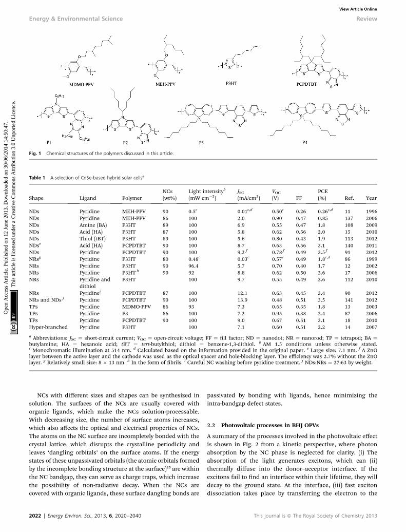
Fig. 1 Chemical structures of the polymers discussed in this article.
Table 1 A selection of CdSe-based hybrid solar cellsa
Shape Ligand PolymerNCs(wt%)
Light intensityb
(mW cm�2)JSC(mA/cm2)
VOC(V) FF
PCE(%) Ref. Year
NDs Pyridine MEH-PPV 90 0.5c 0.01c,d 0.50c 0.26 0.26c,d 11 1996NDs Pyridine MEH-PPV 86 100 2.0 0.90 0.47 0.85 137 2006NDs Amine (BA) P3HT 89 100 6.9 0.55 0.47 1.8 108 2009NDs Acid (HA) P3HT 87 100 5.8 0.62 0.56 2.0 15 2010NDs Thiol (tBT) P3HT 89 100 5.6 0.80 0.43 1.9 113 2012NDse Acid (HA) PCPDTBT 90 100 8.7 0.63 0.56 3.1 140 2011NDs Pyridine PCPDTBT 90 100 9.2 f 0.78 f 0.49 3.5 f 91 2012NRsg Pyridine P3HT 80 0.48c 0.03c 0.57c 0.49 1.8c,d 86 1999NRs Pyridine P3HT 90 96.4 5.7 0.70 0.40 1.7 12 2002NRs Pyridine P3HT h 90 92 8.8 0.62 0.50 2.6 17 2006NRs Pyridine and
dithiolP3HT 100 9.7 0.55 0.49 2.6 112 2010
NRs Pyridinei PCPDTBT 87 100 12.1 0.63 0.45 3.4 90 2012NRs and NDs j Pyridine PCPDTBT 90 100 13.9 0.48 0.51 3.5 141 2012TPs Pyridine MDMO-PPV 86 93 7.3 0.65 0.35 1.8 13 2003TPs Pyridine P3 86 100 7.2 0.95 0.38 2.4 87 2006TPs Pyridine PCPDTBT 90 100 9.0 0.67 0.51 3.1 18 2010Hyper-branched Pyridine P3HT 100 7.1 0.60 0.51 2.2 14 2007
a Abbreviations: JSC ¼ short-circuit current; VOC ¼ open-circuit voltage; FF ¼ ll factor; ND ¼ nanodot; NR ¼ nanorod; TP ¼ tetrapod; BA ¼butylamine; HA ¼ hexanoic acid; tBT ¼ tert-butylthiol; dithiol ¼ benzene-1,3-dithiol. b AM 1.5 conditions unless otherwise stated.c Monochromatic illumination at 514 nm. d Calculated based on the information provided in the original paper. e Large size: 7.1 nm. f A ZnOlayer between the active layer and the cathode was used as the optical spacer and hole-blocking layer. The efficiency was 2.7% without the ZnOlayer. g Relatively small size: 8 � 13 nm. h In the form of brils. i Careful NC washing before pyridine treatment. j NDs:NRs ¼ 27:63 by weight.
Energy & Environmental Science Review
Ope
n A
cces
s A
rtic
le. P
ublis
hed
on 1
2 Ju
ne 2
013.
Dow
nloa
ded
on 3
0/06
/201
4 14
:50:
47.
Thi
s ar
ticle
is li
cens
ed u
nder
a C
reat
ive
Com
mon
s A
ttrib
utio
n 3.
0 U
npor
ted
Lic
ence
.View Article Online
NCs with different sizes and shapes can be synthesized insolution. The surfaces of the NCs are usually covered withorganic ligands, which make the NCs solution-processable.With decreasing size, the number of surface atoms increases,which also affects the optical and electrical properties of NCs.The atoms on the NC surface are incompletely bonded with thecrystal lattice, which disrupts the crystalline periodicity andleaves ‘dangling orbitals’ on the surface atoms. If the energystates of these unpassivated orbitals (the atomic orbitals formedby the incomplete bonding structure at the surface)25 are withinthe NC bandgap, they can serve as charge traps, which increasethe possibility of non-radiative decay. When the NCs arecovered with organic ligands, these surface dangling bonds are
2022 | Energy Environ. Sci., 2013, 6, 2020–2040
passivated by bonding with ligands, hence minimizing theintra-bandgap defect states.
2.2 Photovoltaic processes in BHJ OPVs
A summary of the processes involved in the photovoltaic effectis shown in Fig. 2 from a kinetic perspective, where photonabsorption by the NC phase is neglected for clarity. (i) Theabsorption of the light generates excitons, which can (ii)thermally diffuse into the donor–acceptor interface. If theexcitons fail to nd an interface within their lifetime, they willdecay to the ground state. At the interface, (iii) fast excitondissociation takes place by transferring the electron to the
This journal is ª The Royal Society of Chemistry 2013
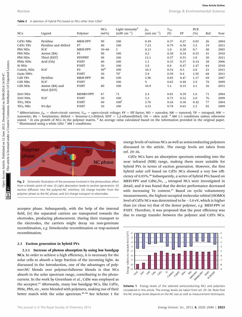
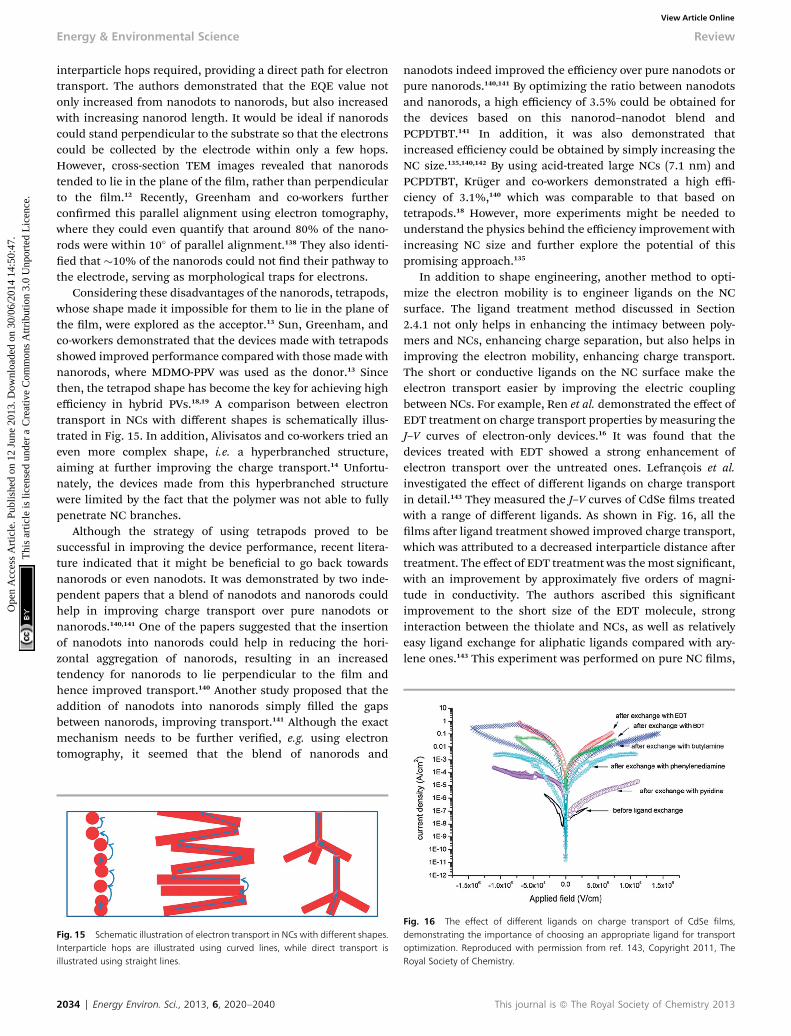
Table 2 A selection of hybrid PVs based on NCs other than CdSea
NCs Ligand PolymerNCs(wt%)
Light intensityb
(mW cm�2)JSC(mA cm�2)
VOC(V) FF
PCE(%) Ref. Year
CdTe NRs Pyridine MEH-PPV 90 100 0.49 0.37 0.27 0.05 26 2004CdTe TPs Pyridine and dithiol P7 80 100 7.23 0.79 0.56 3.2 19 2011PbS NDs N/Ac MEH-PPV 50–60 5 0.13 1.0 0.28 0.7 40 2005PbS NDs Amine (BA) P1 90 100 4.2 0.38 0.34 0.55 41 2010PbS NDs Thiol (EDT) PDTPBT 90 100 13.1 0.57 0.51 3.8 20 2011PbSe NDs Acid (OA) P3HT 80 100 1.1 0.35 0.37 0.14 28 2006Si NDs P3HT 50 100 3.8 0.8 0.47 1.47 64 2010CuInS2 NDs N/Ac P4 90d 100 10.3 0.54 0.5 2.8 21 2011GaAs NWs P3HT 50 70e 5.8 0.59 0.4 1.95 68 2011CdS TPs Pyridine MEH-PPV 86 100 2.96 0.85 0.47 1.17 69 2007CdS NRs N/Ac P3HT 100 9 0.65 0.48 2.9 70 2009CdS NDs Amine (BA) and
thiol (EDT)P3HT 80 100 10.9 1.1 0.35 4.1 16 2011
ZnO NDs MDMO-PPV 67 71 2.4 0.81 0.59 1.6 71 2004ZnO NDs N/Ac P3HT 50 100 5.2 0.75 0.52 2.0 76 2009TiO2 NDs P3HT 60 100f 2.76 0.44 0.36 0.42 77 2004TiO2 NRs N3-dye P3HT 50 100 4.33 0.78 0.65 2.2 82 2009
a Abbreviations: JSC ¼ short-circuit current; VOC ¼ open-circuit voltage; FF ¼ ll factor; ND ¼ nanodot; NR ¼ nanorod; TP ¼ tetrapod; NW ¼nanowire; BA ¼ butylamine; dithiol ¼ benzene-1,3-dithiol; EDT ¼ 1,2-ethanedithiol; OA ¼ oleic acid. b AM 1.5 conditions unless otherwisestated. c In situ growth of NCs in the polymer matrix. d An average value calculated based on the information provided in the original paper.e Illuminated using a white LED. f AM 1 conditions.
Fig. 2 Schematic illustration of the processes involved in the photovoltaic effectfrom a kinetic point of view. (i) Light absorption leads to exciton generation; (ii)exciton diffusion into the polymer:NC interface; (iii) charge transfer from thepolymer phase to the NC phase; and (iv) charge transport to electrodes.
Review Energy & Environmental Science
Ope
n A
cces
s A
rtic
le. P
ublis
hed
on 1
2 Ju
ne 2
013.
Dow
nloa
ded
on 3
0/06
/201
4 14
:50:
47.
Thi
s ar
ticle
is li
cens
ed u
nder
a C
reat
ive
Com
mon
s A
ttrib
utio
n 3.
0 U
npor
ted
Lic
ence
.View Article Online
acceptor phase. Subsequently, with the help of the internaleld, (iv) the separated carriers are transported towards theelectrodes, producing photocurrent. During their transport tothe electrodes, the carriers might decay via non-geminaterecombination, e.g. bimolecular recombination or trap-assistedrecombination.
Scheme 1 Energy levels of the selected semiconducting NCs and polymersconsidered in this article. The energy levels are taken from ref. 29–36. Note thatthe NC energy levels depend on the NC size as well as measurement techniques.
2.3 Exciton generation in hybrid PVs
2.3.1 Increase of photon absorption by using low bandgapNCs. In order to achieve a high efficiency, it is necessary for thesolar cells to absorb a large fraction of the incoming light. Asdiscussed in the Introduction, one of the advantages of poly-mer:NC blends over polymer:fullerene blends is that NCsabsorb in the solar spectrum range, contributing to the photo-current. In the work by Greenham et al., CdSe was employed asthe acceptor.11 Aerwards, many low bandgap NCs, like CdTe,PbSe, PbS, etc., were blended with polymers, making use of theirbetter match with the solar spectrum.26–28 See Scheme 1 for
This journal is ª The Royal Society of Chemistry 2013
energy levels of various NCs as well as semiconducting polymersdiscussed in the article. The energy levels are taken fromref. 29–36.
CdTe NCs have an absorption spectrum extending into thenear infrared (NIR) range, making them more suitable forhybrid PVs in terms of exciton generation. However, the rsthybrid solar cell based on CdTe NCs showed a very low effi-ciency of 0.05%.26 Subsequently, a series of hybrid PVs based onMEH-PPV and CdSexTe1�x tetrapod NCs were investigated indetail, and it was found that the device performance decreasedwith increasing Te content.37 Based on cyclic voltammetrymeasurements, the highest occupied molecular orbital (HOMO)level of CdTe NCs was determined to be�5.0 eV, which is higherthan (or close to) that of the donor polymer, e.g. MEH-PPV orP3HT. Therefore, it was proposed that the poor efficiency wasdue to energy transfer between the polymer and CdTe NCs.
Energy Environ. Sci., 2013, 6, 2020–2040 | 2023

Fig. 3 PIA spectra from P3HT blends with PbSe (green diamonds), PCBM (redcircles), and CdSe (blue squares). No polaronic features are observed forP3HT:PbSe blends. This indicates little charge carrier generation, explaining thepoor device efficiency for polymer:PbSe blends. Reproduced with permission fromref. 45, Copyright 2009, American Chemical Society.
Energy & Environmental Science Review
Ope
n A
cces
s A
rtic
le. P
ublis
hed
on 1
2 Ju
ne 2
013.
Dow
nloa
ded
on 3
0/06
/201
4 14
:50:
47.
Thi
s ar
ticle
is li
cens
ed u
nder
a C
reat
ive
Com
mon
s A
ttrib
utio
n 3.
0 U
npor
ted
Lic
ence
.View Article Online
However, there are other publications reporting low HOMOlevels of �5.5 eV or even �5.8 eV for CdTe NCs.19,38 Thediscrepancy might be caused by different sizes and/or shapes ofthe samples in different measurements, as well as the fact thatcyclic voltammetry is not an accurate method to determine theband position. If the CdTe HOMO level is as low as �5.5 eV,CdTe NCs might still be a good candidate as an acceptormaterial in hybrid PVs. Recently, Chou and co-workers reporteda signicantly improved efficiency of 3.2% for CdTe-basedhybrid solar cells, using a monoaniline-capped polymer as thedonor.19 This might indicate that energy transfer is not themainproblem for the poor efficiency in previous studies.
Further extension of the absorption spectrum into theinfrared regime could be achieved using PbSe or PbS NCs.Sargent and co-workers demonstrated hybrid PVs based on PbSand MEH-PPV.27,39 Unfortunately, the device efficiency was verylow, showing no benet from the infrared absorption. Wattet al. employed a surfactant-free NC synthesis approach, wherethey synthesized PbS NCs directly in the MEH-PPV matrix, andobtained improved efficiency (0.7% under AM 1.5, 5 mW cm�2
illumination).40 Ginger and co-workers used a new donor–acceptor conjugated polymer (P1 in Fig. 1) as the donor in thePbS-based hybrid PVs, and obtained an efficiency of 0.5% undernormal illumination conditions (AM 1.5, 100 mW cm�2).41 Morerecently, by blending PbS NCs with a low bandgap polymer(P2 in Fig. 1), Prasad and co-workers signicantly improved thedevice efficiency to a high value of 3.78%.20
In spite of the improvement in PbS-based hybrid solar cells,the device engineering on PbSe-based hybrid PVs has beendifficult, with a low power conversion efficiency of �0.1% todate.28,42–44 Ginger and co-workers used photoinduced absorp-tion (PIA) spectroscopy to uncover the reason behind this poorefficiency.45 PIA is a quasi-steady-state pump-probe technique,which is useful for detection of long-lived (>10 ms) excited states,such as polarons or triplet excitons. It measures the trans-mittance difference before and aer excitation. If the excitationresults in long-lived species, which give rise to new sub-bandgapoptical transitions, the absorption of these species will leavenon-zero PIA signals in their absorption regime. Fig. 3 showsthe PIA signal of P3HT:PbSe blends, together with those ofP3HT:CdSe and P3HT:PCBM blends for comparison. The PIAspectra for blends of P3HT with CdSe and with PCBM showed abroad absorption from 1.0 to 2.1 eV, with a maximum at�1.25 eV. This agreed well with the polaronic absorptionfeatures of P3HT,46 and hence indicated the generation ofpositive charges in P3HT for these two blends. In contrast, nocharacteristic P3HT polaronic feature was observed in theP3HT:PbSe case, indicating the absence of charge carriergeneration, which explained the poor efficiency of polymer:PbSeblends. However, the absence of long-lived charge transfer inthe PIA spectra does not necessarily mean that the device doesnot work. For example, Ginger and co-workers demonstrated ahybrid solar cell which exhibited photocurrent contributionfrom the absorption of both the polymer and quantum dotcomponents in the absence of a typical spectral signature ofpolymer polarons. They proposed that the device worked as aquantum-dot Schottky diode sensitized by energy transfer from
2024 | Energy Environ. Sci., 2013, 6, 2020–2040
the polymer.47 As a side note, although the efficiency of hybridPVs based on PbSe is low, it has been demonstrated thatPb(Se,S) NC-based quantum dot solar cells show promisingefficiency up to 7%.48–53 Interested readers are referred to acommentary by Sargent.54
In addition to better absorption, using PbSe and PbS NCs inhybrid OPVs is also motivated by their potential for multipleexciton generation (MEG). MEG is based on utilizing hotcarriers to generate one or more additional electron–hole pairs,which can be explained by impact ionization. Nozik proposedthat MEG could be greatly enhanced in NCs compared to bulksemiconductors.55 The formation of two or more excitons perabsorbed photon for PbSe NCs was demonstrated by differentgroups using transient absorption measurements.56–58 Recently,Nozik, Beard and co-workers demonstrated the photocurrentenhancement arising from MEG in PbSe quantum dots-basedsolar cells, as manifested by a peak external quantum efficiency(EQE) exceeding 100%.59 However, the contribution of MEG tothe hybrid solar cell efficiency is not conrmed yet, although itwas claimed that MEG was observed in MEH-PPV:PbSe deviceswith an EQE up to 150% at negative biases.42
Another compelling concept for hybrid solar cells with lowbandgap NCs is singlet exciton ssion.60,61 Singlet excitonssion is a well-established process in organic semiconductorsby which a singlet exciton splits to form two triplet excitons on anearby molecule.62 Singlet exciton ssion could potentiallyovercome the inherently detrimental thermalization lossesassociated with the high energy exciton of organic semi-conductors and the low energy exciton of low bandgap NCs.Pentacene is an attractive material for single exciton ssion,63
because its low relaxed triplet exciton energy is less than half ofthe singlet energy, making the ssion process exothermic.60
Greenham and co-workers fabricated hybrid solar cells made ofpentacene and PbS NCs, harvesting both triplet excitons createdby singlet exciton ssion in pentacene and low-energy excitonsabsorbed by PbS NCs (see Fig. 4 for the device structure and
This journal is ª The Royal Society of Chemistry 2013

Fig. 4 Device structure and energy diagram of hybrid solar cells made of pen-tacene and PbS NCs. Triplet excitons are created by singlet exciton fission inpentacene and low-energy excitons are absorbed by PbS NCs. Reproduced withpermission from ref. 60, Copyright 2012, American Chemical Society.
Review Energy & Environmental Science
Ope
n A
cces
s A
rtic
le. P
ublis
hed
on 1
2 Ju
ne 2
013.
Dow
nloa
ded
on 3
0/06
/201
4 14
:50:
47.
Thi
s ar
ticle
is li
cens
ed u
nder
a C
reat
ive
Com
mon
s A
ttrib
utio
n 3.
0 U
npor
ted
Lic
ence
.View Article Online
energy diagram).60,61 The application of singlet exciton ssion inhybrid solar cells might help to achieve quantum efficienciesover 100%.
There are also reports trying to use other low bandgap NCs asthe acceptor materials, e.g. Si,29,64 Ge,65 CuInSe2,30,66 CuInS2,21,67
GaAs,68 etc. Some of them have demonstrated efficienciesapproaching 3%, worthy of further investigation.
2.3.2 Wide bandgap NCs as acceptor materials. Althoughlow bandgap NCs could potentially increase the absorption, andhence the photocurrent of the device, they usually sacrice theopen-circuit voltage, which is related to the difference betweenthe donor HOMO and acceptor LUMO (lowest unoccupiedmolecular orbital). In addition, as discussed in the previoussection, high HOMO levels of the low bandgap NCs might resultin energy transfer between the polymer and the NCs, whichcould be detrimental to the device performance. Based on thisreasoning, some NCs with relatively wide bandgaps, e.g. CdS,ZnO, TiO2, etc. have also been explored as the acceptor materialsin hybrid PVs.
In the work by Greenham et al., in addition to CdSe, CdS NCswere also considered as acceptor candidates. However, theyfound that the polymer photoluminescence (PL) was notcompletely quenched by CdS NCs, which might be caused byrelatively large phase separation. They did not report the deviceperformance using CdS NCs as the acceptor.11 Cao and co-workers were able to overcome this phase separation problemby choosing a suitable solvent, and they observed signicant PLquenching of the polymer.69 As a result, a reasonably high effi-ciency of 1.17% was achieved for the device based on MEH-PPVand CdS tetrapods. Liao et al. made use of the sulfur atomsalong the backbone of P3HT as anchorage sites for CdS tonucleate and grow, and they synthesized CdS nanorods usingP3HT as a molecular template. Their device showed animproved efficiency of 2.9%.70 More recently, by carefully engi-neering the NC surface as well as the polymer morphology, Renet al. reported a promising efficiency of 4.1% for devices basedon P3HT and CdS nanodots.16
This journal is ª The Royal Society of Chemistry 2013
In spite of their even worse absorption ability than CdS,metal oxides have also attracted intensive interest, due to theirlow cost and non-toxicity. Janssen and co-workers demon-strated that MDMO-PPV:ZnO blends could give an efficiency of1.6% under 71 mw cm�2 white light illumination.71 A relativelylow NC weight ratio (67%) was used in their experiments, asthey noticed that a high concentration of ZnO NCs tended toaggregate in the device. This is because of the poor solubility ofZnO NCs in solvents that dissolve common semiconductingpolymers.72 In a subsequent study, they tried to add a surfactantto ZnO, and changed the NC shape and size, aiming atimproving the device performance. However, the device effi-ciency remained at around 1.6%.73 Even if MDMO-PPV wasreplaced by P3HT, which has higher hole mobility, noimprovement in the device performance was obtained.74 Lateron, the same group employed a method to in situ generate ZnONCs inside organic materials,75 and obtained a record efficiencyof 2.0% for ZnO-based hybrid PVs.76
In addition to ZnO, TiO2 is also explored as the acceptormaterial in hybrid PVs, partially because of its success in dye-sensitized solar cells.1 Kwong et al. blended TiO2 NCs withP3HT, where they optimized the solvent and obtained an effi-ciency of 0.42%.77 In addition to this solvent optimization work,there has been a lot of other device engineering, includingin situ generation of TiO2 inside polymers,78,79 and optimizationof the NC ligand,80 etc. Recently, Chen, Su and co-workersreplaced the insulating surfactant on the NC surface with amore conductive ligand, and increased the device efficiency to1.7%.81 In a subsequent study, they employed a dye to modifythe NC surface, which further increased the PCE to 2.2%.82
Although these kinds of devices including dyes could possiblywork as solid-state dye-sensitized solar cells, the authorsclaimed that their devices remained hybrid PVs based on thefact that no contribution from the dye was observed from theEQE spectra. Indeed, there are other TiO2-based solarcells showing obvious evidence to function as solid-state dye-sensitized solar cells.83–85 This is beyond the scope of this article,and interested readers are referred to a recent review for morediscussions on this issue.22
2.3.3 Improvement of light absorption from the polymerside. There has also been considerable progress on the poly-mer side, aiming at harvesting more light. As mentionedbefore, the polymer used in the initial hybrid PV research wasMEH-PPV,11 which was later replaced by P3HT.86 AlthoughP3HT has a narrower bandgap than MEH-PPV, the improve-ment in terms of light absorption is quite limited. Thedevice performance improvement from MEH-PPV:CdSe toP3HT:CdSe is largely due to the better hole transport ability ofP3HT. A red polyuorene copolymer with a bandgap around1.9 eV (P3 in Fig. 1) was also introduced to the hybrid PVresearch as a low bandgap polymer by Greenham's group. Theyblended it with CdSe tetrapods and obtained an efficiency of2.4%.87 Signicant improvement in light absorption benettedfrom the development of low bandgap polymers extending theabsorption to the NIR regime.88 Among others, PCPDTBT hasbeen extensively explored as an efficient low bandgap donor inhybrid PVs.18,89
Energy Environ. Sci., 2013, 6, 2020–2040 | 2025

Energy & Environmental Science Review
Ope
n A
cces
s A
rtic
le. P
ublis
hed
on 1
2 Ju
ne 2
013.
Dow
nloa
ded
on 3
0/06
/201
4 14
:50:
47.
Thi
s ar
ticle
is li
cens
ed u
nder
a C
reat
ive
Com
mon
s A
ttrib
utio
n 3.
0 U
npor
ted
Lic
ence
.View Article Online
Dayal et al. fabricated a device containing PCPDTBT andCdSe tetrapods, which gave a certied efficiency of �3.1%, therecord efficiency for hybrid solar cells at that time.18 By opti-mizing the NC surface, Kruger and co-workers pushed thisnumber to 3.4%, where they blended PCPDTBT with CdSenanorods.90 Xue and co-workers added a thin ZnO nanoparticlelayer between the cathode and the active layer, which was ablend of PCPDTBT and CdSe nanodots, and they achieved a newrecord efficiency of 3.5%.91 Note that the CdSe NCs used in Xue'swork were nanodots, rather than elongated nanorods or tetra-pods. We will have more discussions on this issue later.Regardless of the CdSe NC shape, since 2010 the record effi-ciency for CdSe-based hybrid PVs has been unexceptionallyachieved using PCPDTBT as the donor, demonstrating theeffectiveness of low bandgap polymers in absorbing more light.Actually, Kruger and co-workers performed a detailed compar-ison between P3HT:CdSe and PCPDTBT:CdSe blends, whereCdSe was in the form of nanodots.89 As shown in Fig. 5a,PCPDTBT extends the absorption to 900 nm, absorbing morelight than P3HT. This absorption enhancement is clearlyobserved in the blend lm absorption spectra (Fig. 5b), andcontributes to the photocurrent (Fig. 5c). As a result,PCPDTBT:CdSe devices demonstrated improved efficiency(2.7%) compared with P3HT:CdSe (2.1%), due to the increase ofshort-circuit current (Fig. 5d).
2.3.4 Harvesting more light by managing the devicearchitecture. From the previous section, we can see that lowbandgap polymers indeed help to capture more light. However,the thickness of normal OPV devices is limited to around100 nm in order to guarantee good charge transport. Althoughorganic materials have a high absorption coefficient, 100 nm isnot enough to absorb all the photons in their absorption
Fig. 5 Comparison between P3HT:CdSe and PCPDTBT:CdSe blends. (a) Absorption sPCPDTBT:CdSe films (87.5 wt% of NCs); (c) EQE spectra of P3HT:CdSe and PCPDTBTcurves of the two devices under a solar simulator (AM 1.5 100 mW cm�2). Reprodu
2026 | Energy Environ. Sci., 2013, 6, 2020–2040
regime. In addition, in a complete device, optical electric eldsare tuned by the optical interference between the incident andback-reected light. As a result, the light intensity is zero at thecathode for a normal device, and a large fraction of the activelayer absorbs little light.92
These problems could be partially solved by optical engi-neering. For example, Xue and co-workers attached a trans-parent hemispherical polymer microlens array (MLA) to thelight incident surface of the device (see Fig. 6a for the scanningelectron micrograph image of the MLA).93 As shown in Fig. 6b,with this array, light striking a microlens will be refracted intothe active layer due to the curved shape of the microlens, whichincreases the optical path length of the device. In addition, lightreecting off one microlens could strike a neighboring one andcontribute to the absorption, which reduces light reectionlosses. With the MLA, they demonstrated that the device effi-ciency of PCPDTBT:CdSe blends could be increased by �30%.93
In addition, this MLA optical approach is not limited to hybridPVs, and could also be applied to other polymer solar cells. Thesame group also employed an optical spacer to increase theoptical absorption in the device.94 Fig. 6c and 6d show acomparison of the calculated optical proles between deviceswithout (Fig. 6c) and with (Fig. 6d) an optical spacer (a layer ofZnO lm).91 The inclusion of a ZnO layer results in optimizedoptical electric eld distribution in the active layer, withsignicantly enhanced light absorption in the NIR regime. Theyfabricated devices and demonstrated that the optical spacerimproved the short-circuit current, and hence the device effi-ciency, by nearly 30%. In addition to this optical contribution,this layer of ZnO might also work as an effective hole-blockinglayer and an exciton dissociation site in the device, whichcollectively gave rise to this 30% improvement.
pectra of P3HT, PCPDTBT, and CdSe films; (b) absorption spectra of P3HT:CdSe and:CdSe devices, where the contribution from PCPDTBT is clearly observed; (d) J–Vced with permission from ref. 89, Copyright 2011, Elsevier.
This journal is ª The Royal Society of Chemistry 2013

Fig. 6 Demonstration of the effect of optical engineering on light absorption. (a)A scanning electron micrograph image of a representative microlens array (MLA);(b) schematic illustration of light behavior with (solid arrows) and without(dashed arrows) an MLA for an organic solar cell. With an MLA, the optical pathlength is increased and the light reflection loss is decreased; (c and d) calculatedlight intensity profiles for the devices without (c) and with (d) an optical spacer (alayer of ZnO film). With an optical spacer, the optical electric field is enhanced inthe active layer. (a and b) Reproduced with permission from ref. 93, Copyright2012, The Royal Society of Chemistry. (cand d) Reproduced with permission fromref. 91, Copyright 2012, The Royal Society of Chemistry.
Review Energy & Environmental Science
Ope
n A
cces
s A
rtic
le. P
ublis
hed
on 1
2 Ju
ne 2
013.
Dow
nloa
ded
on 3
0/06
/201
4 14
:50:
47.
Thi
s ar
ticle
is li
cens
ed u
nder
a C
reat
ive
Com
mon
s A
ttrib
utio
n 3.
0 U
npor
ted
Lic
ence
.View Article Online
In addition, considering the fact that organic materialsusually absorb light within a limited regime, two or more cellswith complementary absorption regimes can be stackedtogether to maximize light absorption. The device with thisstructure is termed as a tandem cell, and has attracted muchattention in polymer:fullerene blends.95,96 However, few reportson the tandem structure exist for hybrid PVs. Recently, Krebsand co-workers demonstrated a tandem cell based on poly-mer:ZnO blends.97 By using thermocleavable polymer materials,they successfully solved the solubility problem during deposi-tion of subsequent layers in the stack, and extended the deviceabsorption over a wide regime. Although the efficiency of theirdevice was low, this work successfully demonstrated the possi-bility of fabricating hybrid PV-based tandem solar cells entirelyby solution processing.
2.4 Exciton diffusion and dissociation in hybrid PVs
Upon photon absorption, strongly bound excitons are gener-ated, with a binding energy around 0.4–0.5 eV.98,99 The excitonsthermally diffuse into the BHJ interfaces, with a diffusionlength around 5–15 nm and a lifetime on the order of nano-seconds,100–105 aer which, they will recombine geminately. Thismeans that donor and acceptor materials have to be well mixedto guarantee efficient exciton dissociation. However, a nemixture will harm charge transport to the electrodes, increasingthe opportunity for oppositely charged carriers to meet andrecombine. As a result, a good balance has to be made to favor
This journal is ª The Royal Society of Chemistry 2013
both charge separation and charge transport. We will discussthis morphology requirement in detail in Section 2.5.1.
Once excitons arrive at the interfaces, the electrons might betransferred to the acceptor. There are two requirements for thischarge transfer process to happen. (1) Since charge transfer is ashort-range interaction that takes place when there is strongwave-function overlap between the donor and acceptor mate-rials, the polymer and NCs must be in close contact with eachother; (2) an energetic offset between the donor and acceptorLUMOs should be guaranteed so that the singlet excitonbinding energy is overcome by this charge transfer process. Forpolymer:fullerene and polymer:polymer blends, condition (1) isusually well satised, and only condition (2) needs to be takencare of. However, for polymer:NC blends, bulky ligands likeoleic acid (OA) or trioctylphosphine oxide (TOPO), necessary forNC synthesis, create a barrier for electron transfer between thepolymer and NCs (see Fig. 7 for chemical structures of theligands mentioned in this article). As a result, condition (1)becomes a serious problem in hybrid PVs. Intensive engi-neering work, including ligand treatments, polymer modica-tion, and direct growth of NCs in polymers, has been devoted tothe interface between polymers and NCs.
2.4.1 Ligand treatments(a) Pyridine treatment of long ligands. Greenham et al.
noticed that long ligands used in the NC synthesis were harmfulto the charge transfer process between polymers and NCs.11 As aresult, ligand exchange processes, where NCs covered with longsynthesis ligands are treated with short ones, are needed toobtain good device performance. They investigated the PLquenching of MEH-PPV:NC blends, where either TOPO-coatedor pyridine-treated NCs were used. With TOPO covered on theNC surface, no PL quenching was observed for MEH-PPV:CdSblends, indicating no electron transfer from MEH-PPV to CdSNCs. However, for the blends where the NC surface was treatedwith pyridine, there was signicant quenching of PL, implyingefficient electron transfer from the polymer to NCs. Differentfrom the CdS case, substantial PL quenching was observedwhen TOPO-coated CdSe NCs were used. As there was a goodoverlap between the MEH-PPV emission spectrum and the CdSeNC absorption spectrum, this PL quenching could be explainedby Forster resonance energy transfer (FRET). The FRET mech-anism is based on a dipole–dipole interaction, and can beobserved with a donor–acceptor distance of several nanome-ters.106 The PL quenching became enhanced aer the ligandexchange process, demonstrating charge transfer from MEH-PPV to CdSe NCs.
This experiment by Greenham et al. showed that it isnecessary to replace long ligands with short ones to ensureeffective charge transfer between polymers and NCs. In addi-tion, it also demonstrated that effective PL quenching does notnecessarily mean efficient charge transfer, as energy transfercould be another route for PL quenching. Since then, ligandexchange using pyridine has been routinely used for hybrid PVfabrication. Later on, it was further demonstrated that thispyridine treatment method could also be applied to hybrid PVsbased on nanorods and tetrapods.12,13 In 2003, the Alivisatosgroup investigated the issue of ligands and PL in more detail
Energy Environ. Sci., 2013, 6, 2020–2040 | 2027

Fig. 7 Chemical structures of the ligands discussed in this article.
Energy & Environmental Science Review
Ope
n A
cces
s A
rtic
le. P
ublis
hed
on 1
2 Ju
ne 2
013.
Dow
nloa
ded
on 3
0/06
/201
4 14
:50:
47.
Thi
s ar
ticle
is li
cens
ed u
nder
a C
reat
ive
Com
mon
s A
ttrib
utio
n 3.
0 U
npor
ted
Lic
ence
.View Article Online
using P3HT:CdSe blends. They found that excess pyridine couldbe removed by pumping the device under low pressure(<10�6 mbar) and/or thermal annealing, due to the low boilingpoint of pyridine.107 The device performance could be signi-cantly improved with the thermal annealing process.
As will be discussed later, pyridine treatment of NCs hasbeen challenged recently, since devices based on NCs treatedwith other short ligands (like amines, thiols, or acids) have beenreported to outperform those based on pyridine-treated NCs.However, more recently, Celik et al. demonstrated a high effi-ciency of 3.4%, where they used PCPDTBT and pyridine-treatedCdSe nanorods.90 The key for this high efficiency was that theNCs were carefully washed in polar and non-polar solventsbefore ligand exchange. Based on transmission electronmicroscopy (TEM) and time-of-ight mass spectrometrymeasurements, they proposed that the washing processremoved weakly bound bulky ligands and made the ligandexchange process more efficient.
(b) Amine treatment of long ligands. In 2005, Sargent and co-workers treated PbS NCs with octylamine, and blended NCswith MEH-PPV.39 Although the device efficiency was low, therewas signicant improvement compared with devices fabricatedfrom OA-coated NCs, demonstrating the effectiveness of aminetreatment. Later on, Carter and co-workers thoroughly inves-tigated P3HT:CdSe blends with different short ligands on theNC surface, including tributylamine, butylamine, and pyri-dine.108 Their comparison concluded that devices based onbutylamine-treated CdSe NCs gave the highest efficiency.Butylamine was also proved to be an effective surfactant forPbS NCs, with polymer:PbS blends demonstrating an efficiencyof over 0.5%.41
2028 | Energy Environ. Sci., 2013, 6, 2020–2040
In addition to these direct treatments of long ligands withshort amines, Prasad and co-workers developed an indirectmethod to reach the aim.109 They replaced the bulky synthesisligand with tert-butyl N-(2-mercaptoethyl)carbamate, which hasa tert-butoxycarbonyl (tBOC) group. The tBOC group releasesisobutene and carbon dioxide during thermal annealing,leaving cysteamine around the NC surface. Although the devicefabricated from this indirect method did not show improve-ment in PCE compared with direct treatment, the authorssuggested that this method led to facile multilayer fabrication,which was useful for tandem cells.
(c) Thiol treatment of long ligands. The development ofcolloidal quantum dot solar cells has benetted a lot from thioltreatment, where a layer-by-layer (LBL) dip-coating process wasemployed for ligand exchange.110,111 The reason for using thisLBL process was that NCs easily got aggregated when thiol-treatment was performed in solution.
Although the LBL process for ligand exchange has not beenused to fabricate hybrid PVs, alternative approaches have beensuccessfully employed to make use of thiols for hybrid PVs. Forexample, in 2008, Cao and co-workers managed to treat TiO2
NCs with thiophenol. They demonstrated that thiophenol-treated NCs quenched polymer PL more efficiently due toenhanced charge transfer.80 As a result, devices based on thio-phenol-treated NCs showed improved performance comparedwith those treated with other ligands. Wu and Zhang managedto perform thiol treatment using a vapor annealing method.112
They spin-coated blends of P3HT and pyridine-treated CdSeNCs, aer which the substrate was le for vapor annealingusing benzene-1,3-dithiol at 120 �C. They employed nuclearmagnetic resonance (NMR) and Fourier transform infrared
This journal is ª The Royal Society of Chemistry 2013

Fig. 8 Schematic illustration of the proposed mechanism for the acid treatmentprocess. Hexanoic acid forms an organic salt with the synthesis ligand(hexadecylamine), effectively reducing the size of the insulating organic layer onthe NC surface. Reproduced with permission from ref. 15, Copyright 2010,American Institute of Physics.
Review Energy & Environmental Science
Ope
n A
cces
s A
rtic
le. P
ublis
hed
on 1
2 Ju
ne 2
013.
Dow
nloa
ded
on 3
0/06
/201
4 14
:50:
47.
Thi
s ar
ticle
is li
cens
ed u
nder
a C
reat
ive
Com
mon
s A
ttrib
utio
n 3.
0 U
npor
ted
Lic
ence
.View Article Online
spectroscopy (FT-IR) experiments to prove that benzene-1,3-dithiol diffused into the blend lm and replaced some of theoriginal ligands during the vapor annealing process. As a result,the short-circuit current and power conversion efficiencyimproved by�70% compared with the control device which wasnot vapor-annealed. This vapor annealing method was bor-rowed by Chou and co-workers.19 Combined with polymer anddevice structure engineering, they achieved a record efficiencyof 3.2% for CdTe-based hybrid PVs. Alternatively, Prasad and co-workers employed a post-ligand exchange method to replace OAligands with 1,2-ethanedithiol (EDT).20 They spin-coated blendsof PDTPBT and OA-coated PbS NCs, aer which EDT solution inacetonitrile was spin-coated on the blend lm to exchange OA.With a layer of TiO2 NCs as the hole-blocking layer beneath thecathode, their device exhibited a high efficiency of 3.78%,signicantly improved compared with previous PbS-basedhybrid PVs.41 Almost published at the same time as Prasad'spaper, Ren et al. reported a high efficiency of 4.1% for hybridPVs based on P3HT and CdS NCs, which were also treated withEDT.16 The P3HT:CdS blend lm, where CdS NCs were alreadytreated with butylamine, was dipped in EDT solution in aceto-nitrile for 30 s and then le for solvent annealing overnight. TheEDT-treated device showed �70% improvement in device effi-ciency compared with the non-treated one.
More recently, Brutchey and co-workers demonstrated thattert-butylthiol-treated CdSe NCs could easily be dissolved intetramethylurea at concentrations up to 100 mg ml�1. Theyblended P3HT with tert-butylthiol-treated CdSe nanodots andobtained an efficiency of 1.9% without any thermal annealingprocess.113 They emphasized that the thiol provides strongerbinding with CdSe NCs compared with an amine or pyri-dine.113,114 As a result, the ligand exchange efficiency using thiolis higher, thereby improving charge transfer. In addition, theyalso found that the LUMO and HOMO levels of NCs changedwith different ligand treatments. The open-circuit voltageincreased to 0.8 V due to a favorable band alignment betweenthe P3HT HOMO and the CdSe LUMO in the tert-butylthiol-treated case.
(d) Acid treatment of long ligands. The bulky synthesis ligandon the NC surface could also be replaced by an acid. Similar totheir approach for exchanging long ligands with thiol,20 Prasadand co-workers used a post-chemical treatment to exchangelong ligands with the acid.115 The lm, spin-coated from asolution made of P3HT and OA-capped PbS NCs, was immersedinto an acetic acid solution for 30 min for ligand exchange. Theyused PL decay to conrm that the charge transfer was enhancedfor the acid-treated lm. As a result, this post-chemical treat-ment resulted in a signicant improvement of the deviceperformance.
An alternative approach is to perform acid treatment beforespin-coating, which was developed by Kruger and co-workersand proved to be a great success.15 The CdSe NCs covered with along synthesis ligand, hexadecylamine (HDA), were washedusing hexanoic acid (HA). The authors proposed that this acidtreatment process resulted in the formation of an organicsalt, effectively removing the ligand HDA (see Fig. 8). Theresulting organic salt was easily separated from the NCs by
This journal is ª The Royal Society of Chemistry 2013
centrifugation. They blended P3HT with the acid-treated CdSenanodots, and obtained a power conversion efficiency of 2%,which was the highest efficiency for devices based on CdSenanodots at that time.15 Later on, they found that this acidtreatment method could also be applied to CdSe NCs coveredwith TOP/OA ligands.89 This experiment demonstrated thegenerality of the acid treatment method. However, consideringthat it is difficult to gure out a reaction between TOP/OA andHA to remove the TOP/OA ligands, more experiments areneeded to understand the exact mechanism of this promisingacid treatment method. It might be possible that this acid-treatment method is a normal ligand-exchange process, ratherthan a chemical reaction.
In addition to these short insulating acid ligands, Chen, Su,and co-workers demonstrated that a conductive acid could alsobe used to enhance the charge transfer between the polymerand NCs.81 They made devices using P3HT and TiO2 nanorods,which were treated with anthracene-9-carboxylic acid (ACA).The ACA molecule consists of an anthracene moiety that isconductive, and has a strong binding energy with TiO2. Fromthe PL lifetimemeasurement, the authors found that the blendsbased on ACA-treated NCs showed shorter time than thosebased on pyridine-treated or OA-capped NCs, demonstratingenhanced charge transfer between P3HT and TiO2 NCs. Indeed,with ACA treatment, the device showed much improvedperformance.
Later on, the same group further extended this idea, and theyused dyes which contained acid groups as the ligand molecules(N3-dye, see Fig. 7 for the chemical structure).82 The employ-ment of dyes in their experiments made the devices functionsimilar to solid state dye-sensitized solar cells, where dyesabsorb light and transfer charges to charge-conducting mate-rials. However, the authors claimed that the dyes in theirexperiments served to help charge transfer (rather than absorblight), which was supported by the fact that there was nocontribution from the dye absorption regime in the EQE spec-trum. They used PL quenching and PL decay experiments todemonstrate that the N3-dye helped in enhancing chargetransfer, and hence increased the photocurrent. In addition,they also showed that these 3D bulky dye ligands could help inslowing down back recombination, which 'increased both theopen-circuit voltage and the photocurrent.
Energy Environ. Sci., 2013, 6, 2020–2040 | 2029

Energy & Environmental Science Review
Ope
n A
cces
s A
rtic
le. P
ublis
hed
on 1
2 Ju
ne 2
013.
Dow
nloa
ded
on 3
0/06
/201
4 14
:50:
47.
Thi
s ar
ticle
is li
cens
ed u
nder
a C
reat
ive
Com
mon
s A
ttrib
utio
n 3.
0 U
npor
ted
Lic
ence
.View Article Online
(e) Ligand treatment efficiency. An interesting result raised inthe above mentioned Kruger's paper is that NMR experimentsrevealed the presence of the synthesis ligand HDA aer acidtreatment.15 Unfortunately, they did not further explore theeffect of the residual HDA ligand on their device performance,possibly due to the difficulty to quantify the amount ofremaining ligand. Anyhow, this information triggered afundamental question: what is the efficiency of these ligandtreatment methods?
As early as the 1990s, Alivisatos' group and Bawendi's groupproved that the ligand exchange of TOPO with pyridine was notcomplete.116,117 Using NMR and thermal gravimetric analysis,Bawendi and co-workers demonstrated that aer ligandexchange, around 90% of the NC surface was covered withligands, 10–15% of which was the long synthesis ligandTOPO.117 Considering that only 30% of the NC surface wascovered with TOPO before ligand exchange, the ligand exchangeefficiency was around 60%. In addition, this value is expected tochange with the size and shape of NCs.116 Holt et al. investigatedligand exchange efficiency by employing FT-IR techniques, andthey found that an amine, thiol or acid was not able tocompletely replace TOPO.118 There are also other reports whichprovided evidence for incomplete exchange of OA using pyri-dine or an amine.119,120 Therefore, it seems that most shortligands cannot completely replace the long synthesis ligandsduring the ligand exchange process.
By collaborating with Kruger's group, Meerholz and co-workers further conrmed that ligand treatment is incompleteusing a physical method.121 Different from previous approaches,where experiments were performed on pure NCs, their experi-ments were performed on polymer:NC blends aer thermalannealing, making their results more relevant to nal devices.They employed spectroscopic ellipsometry and transmissionintensity data to determine the volume ratios between polymersand NCs in polymer:NC blends, where an effective mediumapproximation based on single-component lms was applied.As shown in Fig. 9, the volume ratios (Vpolymer/VNC) in bothblends (P3HT with either pyridine-treated or acid-treated CdSe
Fig. 9 Volume ratios (v¼ Vpolymer/VNC) as a function ofmass ratios (m¼Mpolymer/MNC) for P3HT:CdSe blends, with pyridine-treated (circles) and acid-treated(squares) NCs, where A¼ v/m. The dashed line indicates the ideal casewhere P3HTis blended with uncoated CdSe NCs. The decreased volume ratio comparedwith the ideal case indicates remaining ligands on the NC surface. Data taken fromref. 121.
2030 | Energy Environ. Sci., 2013, 6, 2020–2040
nanodots) were signicantly smaller than in the ideal case,where no ligands were assumed on the NC surface. This resultimplied that there were ligands remaining on the NC surface.These ligands increased the NC volume, and hence decreasedthe volume ratio between the polymer and NCs. Based on somereasonable assumptions on the blend congurations, theyfurther calculated that the ligand layer thickness was �0.9 nmfor pyridine-treated NCs and�0.6 nm for acid-treated ones. Thecalculated organic layers were thicker than the molecular size ofpyridine or HA, which conrmed that the ligand treatment wasnot complete.121
Considering incomplete ligand exchange, it might be bene-cial to have a thorough investigation of the effect of differentligands (including pyridine, amine, thiol, and acid) on thecharge transfer process between the polymer and NCs. Differentligands have different binding affinities with NCs, and hencedifferent abilities to replace the original bulky ligands, whichaffect the charge transfer process. In addition, different ligandsmight bring or remove different amounts of trap sites, whichwill affect charge transport and charge recombination (Section2.5.3). It is desirable to pick up a few ligands which best suitcharge transfer and charge transport processes.
2.4.2 Polymer engineering. In the previous section, wediscussed the efforts searching for short or conductive ligandsto increase the intimacy between polymers and NCs. Anothermethod to reach this aim is to engineer polymers. The basicidea is to add a functional group (e.g. acid, ester, amino, aniline,or thiol) to the polymer so that these functional groups replacepart of ligands on the NC surface (see Fig. 10 for chemicalstructures of functionalized polymers and oligomers discussedin this article). In addition to enhancing charge transferbetween the polymer and NCs, this approach could also helpNCs to disperse uniformly in the polymer matrix.
In 2003, Alivisatos, Frechet, and co-workers added phos-phonic acid binding groups to oligothiophenes (O1 in Fig. 10),which were then used as ligands for CdSe NCs.122 Theydemonstrated that the oligomers with ve or more thiophenerings underwent charge transfer with CdSe NCs. Although theydid not measure the photovoltaic effect of these oligothiophe-ne:CdSe complexes, they proposed that these complexes couldwork as solar cells by themselves. In addition, they alsoproposed that that these modied oligothiophenes could beused as a third component in a polymer:NC blend to enhanceelectronic coupling between polymers and NCs. Indeed, oneyear later, Locklin et al. employed a similar strategy and addedphosphonic acid binding groups to conjugated oligothiophenedendrons (O2 in Fig. 10).123 They demonstrated that thesedendron:NC complexes worked as solar cells on their own, with0.29% power conversion efficiency under 0.14 mW cm�2 illu-mination. The other idea proposed by Alivisatos to use thesemodied oligomers as a third component to mediate theinteraction between polymers and NCs was also realizedrecently. Chen, Su, and co-workers synthesized a bromine-terminated thiophene oligomer (O3 in Fig. 10), which was usedto enhance electronic coupling between P3HT and TiO2 NCs.Improved device performance was observed for P3HT:TiO2
blends with this third component.124
This journal is ª The Royal Society of Chemistry 2013

Fig. 10 Chemical structures of the polymers and oligomers with functional groups which help them to attach to NCs. The functional groups are illustrated in shadow.
Review Energy & Environmental Science
Ope
n A
cces
s A
rtic
le. P
ublis
hed
on 1
2 Ju
ne 2
013.
Dow
nloa
ded
on 3
0/06
/201
4 14
:50:
47.
Thi
s ar
ticle
is li
cens
ed u
nder
a C
reat
ive
Com
mon
s A
ttrib
utio
n 3.
0 U
npor
ted
Lic
ence
.View Article Online
Alivisatos and co-workers also employed this strategy inpolymers. They added amino groups to polythiophene (P5 inFig. 10) to increase the miscibility between polymers and NCs.125
When blended with CdSe NCs, the modied polythiopheneshowed improved performance compared with the controlpolymer. Based on TEM images, they believed that the perfor-mance improvement was due to enhanced intimacy andimproved morphology. Janssen and co-workers conrmed thisintimacy induced by the polymer functional groups usingelectron tomography.126 Electron tomography makes it possibleto reconstruct the 3D networks of the active layer, providingcritical morphological parameters that are valuable forimproving the device performance.127 They added ester groupsto polythiophene (P6 in Fig. 10) as the donor and used ZnO NCsas the acceptor. Using electron tomography, they could visualizethe effect of the ester groups on the intermixing of the twomaterials in 3D. As shown in Fig. 11, the images clearly conrmthat ZnO NCs disperse much better in P6 than in the controlpolymer, P3HT. Their photo-induced absorption experimentsrevealed that this intimacy enhanced charge transfer, and hencecharge generation for the P6:NC blends. Recently, this func-tional group approach was also used to fabricate highly efficientCdTe-based hybrid OPVs, where aniline groups on the polymer(P7 in Fig. 10) served as a strong anchor to attach to CdTe NCs.19
Fig. 11 Reconstructed volumes from electron tomography for (a) P3HT:ZnO and(b) P6:ZnO. ZnO appears yellow, and the polymer looks transparent against ablack background. It is clear that amino groups in P6 help NCs disperse muchbetter in the polymer matrix. Reproduced with permission from ref. 126,Copyright 2011, WILEY-VCH Verlag GmbH & Co. KGaA, Weinheim.
This journal is ª The Royal Society of Chemistry 2013
These functional groups were also used to fabricate hybridOPVs made of single nanowires by Yang, Frechet, and co-workers (see Fig. 12 for device structure).128 End-functionalizedoligo- or poly-thiophene (O4 and P8 in Fig. 10) was graed ontoZnO nanowires. This single core–shell nanowire (ZnO core andthiophene shell) demonstrated photovoltaic behavior, indi-cating efficient charge generation and transport.
2.4.3 Avoiding ligand issues – in situ NC formation. Asdiscussed in the previous two sections, ligands, necessary tostabilize NCs in solution, require much engineering andunderstanding to minimize their detrimental effects on thedevice performance. In this sense, a ligand-free approach tofabricate hybrid PVs might be helpful. NCs could be in situprepared from annealing a solution which contains a conju-gated polymer and precursor materials for NCs. Alternatively,NCs could also be in situ synthesized using the polymer as atemplate before lm deposition. For both cases, no ligandis needed.
The in situ NC formation approach was initiated by Janssen'sgroup.78 They prepared blends of MDMO-PPV and a titaniumprecursor. The titanium precursor formed TiO2 within thepolymer matrix via hydrolysis in air. The authors conrmedcharge transfer from the polymer to TiO2 using PIA experi-ments. The devices demonstrated photovoltaic response, with apeak EQE around 11%. By optimizing the ratio between thepolymer and TiO2, they improved the power conversion effi-ciency to �0.2%.79 The relatively low efficiency of the devicewas limited by the amorphous nature of TiO2. Although
Fig. 12 (a) Schematic illustration and (b) SEM image of a hybrid nanowire PVwith the core–shell structure (ZnO core and thiophene shell). In the inset of (b) is aTEM image of the core–shell structure. Reproduced with permission from ref. 128,Copyright 2010, American Chemical Society.
Energy Environ. Sci., 2013, 6, 2020–2040 | 2031

Energy & Environmental Science Review
Ope
n A
cces
s A
rtic
le. P
ublis
hed
on 1
2 Ju
ne 2
013.
Dow
nloa
ded
on 3
0/06
/201
4 14
:50:
47.
Thi
s ar
ticle
is li
cens
ed u
nder
a C
reat
ive
Com
mon
s A
ttrib
utio
n 3.
0 U
npor
ted
Lic
ence
.View Article Online
crystallization of TiO2 could be achieved by annealing the lmat temperatures over 350 �C, high temperatures will destroy thepolymer. To overcome this problem, they switched to the ZnOprecursor, considering that ZnO could crystallize at lowtemperatures. By annealing a solution containing MDMO-PPVand a ZnO precursor at 110 �C, they obtained devices with a PCEof over 1%, which was improved compared to the TiO2 case.75
However, Blom and co-workers noticed that MDMO-PPVdegraded in the presence of a TiO2 precursor (diethylzinc).129
Based on UV-vis spectroscopy and charge-transport studies,they proposed that trans vinyl bonds in the PPV backbone brokeand converted to a non-conjugated species, which limited thedevice performance. They avoided this degradation by usingP3HT, which does not contain vinyl moieties and is more stablethan MDMO-PPV. The devices based on P3HT showed a powerconversion efficiency of 1.4%, higher than the MDMO-PPV case.By optimizing the active layer thickness, Janssen and co-workersfurther improved the efficiency to 2%, which is the record effi-ciency for ZnO-based hybrid PVs currently.76 Aided by electrontomography, they identied that the relatively poor efficiency ofthin devices was related to low charge carrier generation as wellas exciton quenching at the electrodes. For thicker devices, thedevice performance was improved as a result of favorable phaseseparation, although increasing thickness resulted in difficul-ties to collect charge carriers.
In addition to metal oxides, in situ formation was alsosuccessfully employed to prepare metal chalcogenides. Thegrowth of lead chalcogenide in a polymer matrix was rstreported by Watt et al.130,131 Although the photovoltaic effect wasnot measured in their initial reports, they used PL quenchingexperiments to demonstrate charge transfer between polymersand NCs. In a following study, they reported a power conversionefficiency of 0.7% for devices based on PbS NCs synthesized inMEH-PPV.40 A considerable improvement in device efficiencywas made by Liao et al., who made use of the P3HT chain as atemplate to synthesize CdS nanorods and obtained a PCE of2.9% (see Fig. 13 for the synthesis mechanism).70 The aspectratio of CdS nanorods could be controlled by varyingthe cosolvent ratio during synthesis. Their results also
Fig. 13 Schematic illustration of in situ growth of CdS nanorods in the P3HTmatrix. Cd ions in the cadmium precursor couples with unpaired S atoms alongthe P3HT chain. Following addition of the sulfur precursor, CdSe starts to nucleateand grows along the P3HT chain, forming nanorods. Reproduced with permissionfrom ref. 70, Copyright 2009, American Chemical Society.
2032 | Energy Environ. Sci., 2013, 6, 2020–2040
demonstrated enhanced PL quenching and improved perfor-mance with increasing NC aspect ratio.
Note that there is difference between the synthesis methodused by Watt or Liao and that by Janssen or Blom. For theformer, the NCs were already formed before spin-coating thelm, while for the latter, NCs were formed by decomposition ofthe precursor during and aer the deposition process. In prin-ciple, the latter method is more convenient because it does notrequire a NC synthesis process before lm deposition. Recently,Haque and co-workers reported P3HT:CdS devices fabricatedfrom thermal decomposition of a cadmium xanthate precursorin a P3HT lm.132 The key point in this work was that onlyvolatile decomposition products were produced so that no by-products were le in the nal device. Using transient absorp-tion, they demonstrated that their lms exhibited the genera-tion of long-lived charges, indicating efficient charge transfer.The PCE of the initial device was 0.72%, which was increased to2.17% by optimizing the thermal annealing temperature of thecomposite lm.133 They also applied this method to the fabri-cation of polymer:CuInS2 devices, and obtained a high effi-ciency of 2.8%,21 which is much improved compared with theprevious work based on CuInS2 NCs.67
2.5 Charge transport and collection
Aer exciton dissociation, holes are le on the donor phaseand electrons are transferred to the acceptor phase. For poly-mer:fullerene and polymer:polymer blends, due to weakscreening of the electric eld, a strong coulombic attraction stillexists for these electron–hole pairs (known as charge-transferstates).134 The charge-transfer states could decay geminately,being a loss to the photocurrent. However, this geminate decayof charge-transfer states is less likely to occur for hybrid PVs,considering the large dielectric constant of inorganic NCs. Inother words, the electron and hole dissociated from an excitonare relatively free from each other. Indeed, recent transientabsorption measurements indicated that polarons barelydecayed between 1 and 100 ns for devices based on P3HT andCdSe nanodots.135 This means that geminate loss is not adominant loss mechanism for hybrid PVs.
These free charges have to be transported to the electrodes,so that they can contribute to the photocurrent. Ideally, ahighway is needed for electrons and holes to their respectiveelectrodes. However, in a BHJ structure, it is difficult to guar-antee such a percolation path. As a result, the charge transportto the electrodes could be severely hindered by parameters likemorphology, mobility, and traps, which have to be optimized.
2.5.1 Morphology optimization. Due to the complexmorphology of the BHJ structure, free electrons and holes couldmeet each other on their way to the electrodes, and recombine.This recombination between two free oppositely chargedcarriers is termed as bimolecular recombination. Actually, forthe sake of charge transport, to 'large phases are favorable.However, as discussed before, small phases are needed to makesure that excitons can reach an interface to dissociate within thediffusion length. As a result, the morphology has to be opti-mized so that the balance between charge separation and
This journal is ª The Royal Society of Chemistry 2013

Review Energy & Environmental Science
Ope
n A
cces
s A
rtic
le. P
ublis
hed
on 1
2 Ju
ne 2
013.
Dow
nloa
ded
on 3
0/06
/201
4 14
:50:
47.
Thi
s ar
ticle
is li
cens
ed u
nder
a C
reat
ive
Com
mon
s A
ttrib
utio
n 3.
0 U
npor
ted
Lic
ence
.View Article Online
charge transport can be achieved. Although we discuss themorphology in this ‘Charge transport and collection’ section,we have to stress that morphology is of the same importance toexciton dissociation. The morphology of hybrid PVs could beaffected by many different factors, including the solvent,107,136,137
thermal annealing,69 the ligand on the NC surface,108 the sizeand shape of NCs,138 weight ratio between polymers andNCs,74,75 polymer molecule weight,139 vapor annealing,19,112 lmthickness,73,76 functional group on the polymer,126 etc.
Alivisatos and co-workers have shown that the solvent had asignicant effect on the lm morphology, and hence the deviceefficiency.107 A two solvent mixture approach, where one was agood solvent for NCs and the other was a good solvent for thepolymer, was used to control the morphology down tothe nanometer scale. As shown in Fig. 14a, by optimizing thevolume ratio between chloroform (a good solvent for the poly-mer) and pyridine (a good solvent for NCs), they could increase
Fig. 14 The effect of solvents on the film morphology and device performance.(a) The device EQE value could be maximized by controlling the volume ratio inbinary solvent blends, where the active layer was composed of P3HT and CdSenanorods; (b) different solvents (TCB is short for 1,2,4-trichlorobenzene) for thepolymer resulted in different J–V curves (one sun conditions) for blends of MDMO-PPV and CdSe tetrapods, demonstrating the importance of choosing an appro-priate solvent for the polymer. (a) Reproduced with permission from ref. 107,Copyright 2003, WILEY-VCH Verlag GmbH & Co. KGaA, Weinheim. (b) Repro-duced with permission from ref. 136, Copyright 2004, American Institute ofPhysics.
This journal is ª The Royal Society of Chemistry 2013
the EQE value by a factor of 1.4. They further demonstrated thatthis optimized volume ratio was dependent on the shape andsize of NCs, as a result of different non-passivated Cd surfacesites on different samples. In addition to the ratio betweenmixed solvents, Sun, Greenham, and co-workers demonstratedthat choosing an appropriate solvent for the polymer was alsocrucial for the lm morphology.136 They investigated the effectof different solvents on the performance of devices based onMDMO-PPV and CdSe tetrapods. As shown in Fig. 14b, theyfound that a high boiling point solvent (1,2,4-trichlorobenzene)resulted in much improved efficiency compared with a lowboiling point solvent (chloroform). They proposed that slowevaporation of the high boiling point solvent gave rise tofavorable phase separation between the polymer and NCs,which was benecial to charge transport.
Janssen and co-workers employed electron tomography toinvestigate the effect of thickness on the lm morphology,where ZnO NCs were in situ formed in the P3HT matrix.76 Theauthors found considerable difference between lms withdifferent thicknesses. The thin lm showed very large polymerdomains, with the domain size signicantly larger than theexciton diffusion length. With increasing lm thickness, theyobserved ner phase separation between the donor and theacceptor. As we said before, large phase separation benetscharge transport while small phase separation benets excitondissociation. This experiment by Janssen's group demonstratedthat a balance had to be reached between these two processes inorder to maximize the device performance. They found that theoptimized thickness for their device was �225 nm, above whichthe disadvantage of transporting charge carriers outweighed theadvantage of generating more charges. As discussed in Section2.4.2, the same group also used electron tomography to inves-tigate the effect of polymer functional groups on the lmmorphology (see Fig. 11).126 Consistent with this thickness-dependence work, although polymer functional groupsenhanced the intimacy between the polymer and NCs, andhence improved exciton dissociation, this intimacy was detri-mental for thick devices as it hindered charge transport.
2.5.2 Mobility optimization. In the seminal work byGreenham et al., it was pointed out that the charge mobilitymust be large enough so that the carriers could be removedfrom the device before they recombined at the interfacesbetween the donor and acceptor.11 They noticed that at 40 wt%of NCs, the PL of the polymer was already quenched by a factorof 10, indicating that at least 90% of excitons dissociated at thisratio. However, the EQE value at 40 wt% of NCs was almost afactor of 10 smaller than that at 90 wt% of NCs. They attributedthe device performance improvement between 40 and 90 wt% ofNCs mainly to improved electron mobility. Since electrons aretransported by a hopping mechanism between NCs, anincreasing amount of NCs in the lm shortened the distancebetween NCs, and hence helped electron transport.
Inspired by this idea, much engineering work has beendevoted to improving the transport between NCs. A signicantimprovement was made by Alivisatos and co-workers, whoreplaced nanodots with nanorods and obtained a PCE of 1.7%.12
The idea behind it was that nanorods reduced the number of
Energy Environ. Sci., 2013, 6, 2020–2040 | 2033
Energy & Environmental Science Review
Ope
n A
cces
s A
rtic
le. P
ublis
hed
on 1
2 Ju
ne 2
013.
Dow
nloa
ded
on 3
0/06
/201
4 14
:50:
47.
Thi
s ar
ticle
is li
cens
ed u
nder
a C
reat
ive
Com
mon
s A
ttrib
utio
n 3.
0 U
npor
ted
Lic
ence
.View Article Online
interparticle hops required, providing a direct path for electrontransport. The authors demonstrated that the EQE value notonly increased from nanodots to nanorods, but also increasedwith increasing nanorod length. It would be ideal if nanorodscould stand perpendicular to the substrate so that the electronscould be collected by the electrode within only a few hops.However, cross-section TEM images revealed that nanorodstended to lie in the plane of the lm, rather than perpendicularto the lm.12 Recently, Greenham and co-workers furtherconrmed this parallel alignment using electron tomography,where they could even quantify that around 80% of the nano-rods were within 10� of parallel alignment.138 They also identi-ed that �10% of the nanorods could not nd their pathway tothe electrode, serving as morphological traps for electrons.
Considering these disadvantages of the nanorods, tetrapods,whose shape made it impossible for them to lie in the plane ofthe lm, were explored as the acceptor.13 Sun, Greenham, andco-workers demonstrated that the devices made with tetrapodsshowed improved performance compared with those made withnanorods, where MDMO-PPV was used as the donor.13 Sincethen, the tetrapod shape has become the key for achieving highefficiency in hybrid PVs.18,19 A comparison between electrontransport in NCs with different shapes is schematically illus-trated in Fig. 15. In addition, Alivisatos and co-workers tried aneven more complex shape, i.e. a hyperbranched structure,aiming at further improving the charge transport.14 Unfortu-nately, the devices made from this hyperbranched structurewere limited by the fact that the polymer was not able to fullypenetrate NC branches.
Although the strategy of using tetrapods proved to besuccessful in improving the device performance, recent litera-ture indicated that it might be benecial to go back towardsnanorods or even nanodots. It was demonstrated by two inde-pendent papers that a blend of nanodots and nanorods couldhelp in improving charge transport over pure nanodots ornanorods.140,141 One of the papers suggested that the insertionof nanodots into nanorods could help in reducing the hori-zontal aggregation of nanorods, resulting in an increasedtendency for nanorods to lie perpendicular to the lm andhence improved transport.140 Another study proposed that theaddition of nanodots into nanorods simply lled the gapsbetween nanorods, improving transport.141 Although the exactmechanism needs to be further veried, e.g. using electrontomography, it seemed that the blend of nanorods and
Fig. 15 Schematic illustration of electron transport in NCs with different shapes.Interparticle hops are illustrated using curved lines, while direct transport isillustrated using straight lines.
2034 | Energy Environ. Sci., 2013, 6, 2020–2040
nanodots indeed improved the efficiency over pure nanodots orpure nanorods.140,141 By optimizing the ratio between nanodotsand nanorods, a high efficiency of 3.5% could be obtained forthe devices based on this nanorod–nanodot blend andPCPDTBT.141 In addition, it was also demonstrated thatincreased efficiency could be obtained by simply increasing theNC size.135,140,142 By using acid-treated large NCs (7.1 nm) andPCPDTBT, Kruger and co-workers demonstrated a high effi-ciency of 3.1%,140 which was comparable to that based ontetrapods.18 However, more experiments might be needed tounderstand the physics behind the efficiency improvement withincreasing NC size and further explore the potential of thispromising approach.135
In addition to shape engineering, another method to opti-mize the electron mobility is to engineer ligands on the NCsurface. The ligand treatment method discussed in Section2.4.1 not only helps in enhancing the intimacy between poly-mers and NCs, enhancing charge separation, but also helps inimproving the electron mobility, enhancing charge transport.The short or conductive ligands on the NC surface make theelectron transport easier by improving the electric couplingbetween NCs. For example, Ren et al. demonstrated the effect ofEDT treatment on charge transport properties by measuring theJ–V curves of electron-only devices.16 It was found that thedevices treated with EDT showed a strong enhancement ofelectron transport over the untreated ones. Lefrançois et al.investigated the effect of different ligands on charge transportin detail.143 They measured the J–V curves of CdSe lms treatedwith a range of different ligands. As shown in Fig. 16, all thelms aer ligand treatment showed improved charge transport,which was attributed to a decreased interparticle distance aertreatment. The effect of EDT treatment was themost signicant,with an improvement by approximately ve orders of magni-tude in conductivity. The authors ascribed this signicantimprovement to the short size of the EDT molecule, stronginteraction between the thiolate and NCs, as well as relativelyeasy ligand exchange for aliphatic ligands compared with ary-lene ones.143 This experiment was performed on pure NC lms,
Fig. 16 The effect of different ligands on charge transport of CdSe films,demonstrating the importance of choosing an appropriate ligand for transportoptimization. Reproduced with permission from ref. 143, Copyright 2011, TheRoyal Society of Chemistry.
This journal is ª The Royal Society of Chemistry 2013

Fig. 17 Temporal evolution of ESR signals, where the start of light excitation ismarked as * and the termination of light excitation is marked as **. In contrast tothe fast decay of P3HT:PCBM blends, P3HT:CdSe exhibits persistent decay, sug-gesting the presence of deep traps. Reproduced with permission from ref. 146,Copyright 2009, WILEY-VCH Verlag GmbH & Co. KGaA, Weinheim.
Review Energy & Environmental Science
Ope
n A
cces
s A
rtic
le. P
ublis
hed
on 1
2 Ju
ne 2
013.
Dow
nloa
ded
on 3
0/06
/201
4 14
:50:
47.
Thi
s ar
ticle
is li
cens
ed u
nder
a C
reat
ive
Com
mon
s A
ttrib
utio
n 3.
0 U
npor
ted
Lic
ence
.View Article Online
rather than polymer:NC blend lms. However, it demonstratedthe importance of choosing appropriate ligands to optimize theelectron transport.
Althoughmuch attention has been focused on improving theelectron transport, in principle, the hole transport is of equalimportance. P3HT could form bril structures under certainprocessing conditions, with good p–p stacking along the briland improved mobility.144 Sun and Greenham made use of this,and demonstrated that by using a high boiling point solvent toinduce the P3HT bril formation, the P3HT:CdSe device effi-ciency could be increased by a factor of around 50%.17 A similarstrategy was also employed by Ren et al. to improve theperformance of P3HT:CdS devices.16
2.5.3 Trap investigation. On their way transporting to theelectrodes, in addition to recombining with free oppositelycharged carriers, the charge carriers could also be trapped. Thetrap states could be morphological in nature, arising fromindividual NCs or NC clusters isolated by polymers. With elec-tron tomography, it has been demonstrated that morphological“dead ends” do exist in devices based on nanodots as well asthose based on nanorods.76,138 Alternatively, the trap statescould also be energetic in nature, arising from defects orunpassivated NC surfaces. The trapped charge carriers willserve as recombination sites if they could not escape from thetrap states quickly. They could also build up unfavorable spacecharges in the active layer, affecting the electric eld distribu-tion within the device. Both effects are known to be harmful tothe photocurrent. In addition, the trap states could also affectthe quasi-Fermi level of NCs, being harmful to the open-circuitvoltage.135 In spite of these detrimental effects of traps on thedevice performance, the traps in hybrid PVs are less investi-gated and poorly understood, maybe due to the lack of tech-niques to quantify the trap effects. In this sub-section, we willdiscuss some techniques which have been employed to quali-tatively investigate the trap effects in hybrid PVs.
Actually, in the original paper by Greenham et al., the effectof traps on the device has been mentioned.11 They observed thatat intensities up to 10 W m�2, the short-circuit current wasapproximately linear with the illumination intensity. The lineardependence of current on light intensity is characteristic ofrecombination at a xed number of recombination sites,consistent with recombination mediated by trap states.
Another technique to investigate traps is PIA spectroscopy.In Section 2.3.1, we have discussed PIA as a useful tool toqualitatively examine whether long-lived charge carriers aregenerated in a system. Actually, PIA could also help in obtaininginformation on the lifetime distribution and recombinationdynamics of these charge carriers by varying the excitationfrequency. If lifetimes of charge carriers exceed the inverse ofexcitation frequency, their absorption will be suppressed in thePIA signal. Using this technique, Ginger and Greenham foundthat the lifetime of charge carriers spanned a wide range fromless than 100 ms to more than several ms for MEH-PPV:CdSeblends.145 The lifetime exceeding several ms was consistent withthe presence of trapped charge carriers, which resulted in slowrecombination and long lifetime. Similar wide distribution oflifetimes was also reported for P3:CdSe blends.87 The authors
This journal is ª The Royal Society of Chemistry 2013
found that a model for dispersive recombination, whichaccounted for the effects of traps, had to be employed to t theirdata. Using the same technique, Heinemann et al. comparedthe recombination for P3HT:PCBM and P3HT:CdSe blends.They also found that the model for dispersive recombinationhad to be used for tting the P3HT:CdSe data, while a bimo-lecular recombination could t the P3HT:PCBM data well. Thisfurther conrmed signicant effects of traps on the operation ofhybrid PVs.146 In addition, transient absorption spectroscopy, atechnique similar to PIA but extending to short time regimes,was also employed to demonstrate the presence of considerabletrap states in hybrid PVs.135,147–149
In addition to PIA spectroscopy, Heinemann et al. usedanother technique, electron spin resonance (ESR), to furthercompare the difference between P3HT:PCBM and P3HT:CdSeand demonstrate the effects of traps on hybrid PVs.146 ESR is auseful technique to detect states with a non-zero spin, such aspolarons or triplet excitons. By comparing the ESR signal beforeand aer light excitation of the sample, it is possible to examinewhether successful charge separation occurs in PVs. In addi-tion, by observing the decay of light-induced ESR signals aerswitching off the light excitation, it is possible to examine therecombination dynamics of these light-induced charge carriers.As shown in Fig. 17, aer light excitation, both P3HT:PCBM andP3HT:CdSe samples showed increased ESR signals, indicatingsuccessful charge transfer for both cases. For P3HT:PCBM, arapid decay of the ESR signal was observed upon turning off thelight excitation, indicating fast recombination of the generatedcharge carriers. In contrast, P3HT:CdSe showed complex decaydynamics, which was a superposition of a prompt decay in thesubsecond regime and a persistent decay in the hour regime.The fast decay could be explained by bimolecular recombina-tion between free charge carriers. The remaining charge carriersare deeply trapped, resulting in slow recombination andpersistent decay.
Recently, Greenham and co-workers used transient photo-current and photovoltage measurements to investigate the
Energy Environ. Sci., 2013, 6, 2020–2040 | 2035

Fig. 18 Transient short-circuit photocurrent for P3HT:PCBM blends (a and b) and P3HT:CdSe blends (c and d) at various intensities. (a and c) show the raw data, and (band d) present normalized curves. Compared with P3HT:PCBM, the slow rise and decay of P3HT:CdSe indicate the presence of a large amount of charge traps.Reproduced with permission from ref. 150, Copyright 2011, WILEY-VCH Verlag GmbH & Co. KGaA, Weinheim.
Energy & Environmental Science Review
Ope
n A
cces
s A
rtic
le. P
ublis
hed
on 1
2 Ju
ne 2
013.
Dow
nloa
ded
on 3
0/06
/201
4 14
:50:
47.
Thi
s ar
ticle
is li
cens
ed u
nder
a C
reat
ive
Com
mon
s A
ttrib
utio
n 3.
0 U
npor
ted
Lic
ence
.View Article Online
trap effects in hybrid PVs.135,150 Transient photocurrentmeasurements examine how the photocurrent responds topulsed light illumination, providing useful information oncharge transport, recombination and lifetime. Examining thelight-intensity dependence of photocurrent response helps inrevealing information on non-linear processes such as trap-ping and detrapping. Similar to PIA and ESR measurements,transient photocurrent measurements focus on long-livedspecies, suitable for investigating trapping effects. Fig. 18compares transient photocurrent data for P3HT:PCBM andP3HT:CdSe devices under different light intensities. ForP3HT:PCBM devices, fast turn-on and turn-off dynamics wereobserved under all the intensities investigated (Fig. 18a), withlittle change in the shape of curves (Fig. 18b), which wasconsistent with a relatively trap-free transport. In contrast, forP3HT:CdSe devices, both turn-on and turn-off dynamics werecomposed of fast and slow components (Fig. 18c and d). Theslow components could be explained by the presence of a largeamount of trap states. With increasing light intensity, anincreasing amount of trap states was lled, which reduced thetime to reach the steady state. Further examination of thetransient photocurrents at different biases revealed that trap-ping effects were getting increasingly severe approaching theopen-circuit voltage, maybe due to the eld-dependentdetrapping rate. The authors also examined the trappingeffects using transient photovoltage measurements.150 Tran-sient photovoltage measurements examine the voltage decayaer a small perturbative light pulse for a device workingunder open circuit conditions. It is a direct measure of chargerecombination kinetics under open-circuit conditions. Thephotovoltage measurements further demonstrated that theextraction of trapped charges was a limiting process forP3HT:CdSe devices.
2036 | Energy Environ. Sci., 2013, 6, 2020–2040
Though qualitative, all the above techniques revealed thedetrimental effects of traps on the performance of hybrid PVs,particularly by comparing the behaviors between poly-mer:PCBM and polymer:NC devices. Further investigation isneeded to help us further understand the trapping effects andimprove the performance of hybrid PVs.
3 Conclusions and outlook
Although there was a bottleneck for the development of hybridPVs with the efficiency saturating at�3% for a long time,31 thesetwo years have witnessed the renaissance of this area. Powerconversion efficiency exceeding 4% has been reported. Inaddition to CdSe, devices based on other NCs, including CdS,CdTe, PbS, TiO2, and CuInS2, also demonstrated promisingefficiencies. These processes are encouraging, particularlyconsidering that much fewer groups are working on poly-mer:NC blends than polymer:fullerene blends.
Compared with polymer:fullerene devices, the polymer:NCdevices seem to be limited by charge transfer and chargetransport. In this sense, the ligands on the NC surface play asignicant role in determining the device efficiency, since theyaffect both charge transfer and charge transport processes. Inspite of the recent success in exploring alternative ligands topyridine, more experiments are needed to understand howthese ligands affect the polymer:NC interaction as well as theinteraction between NCs. In addition, the effects of ligands onsurface traps have to be investigated in more detail, so thatrecombination through trap states could be minimized.151
Alternative approaches, like direct growth of NCs in a polymermatrix, might also deserve further attention, due to theirobvious advantages of bypassing ligand problems and theirrecent success in fabricating highly efficient devices. Another
This journal is ª The Royal Society of Chemistry 2013
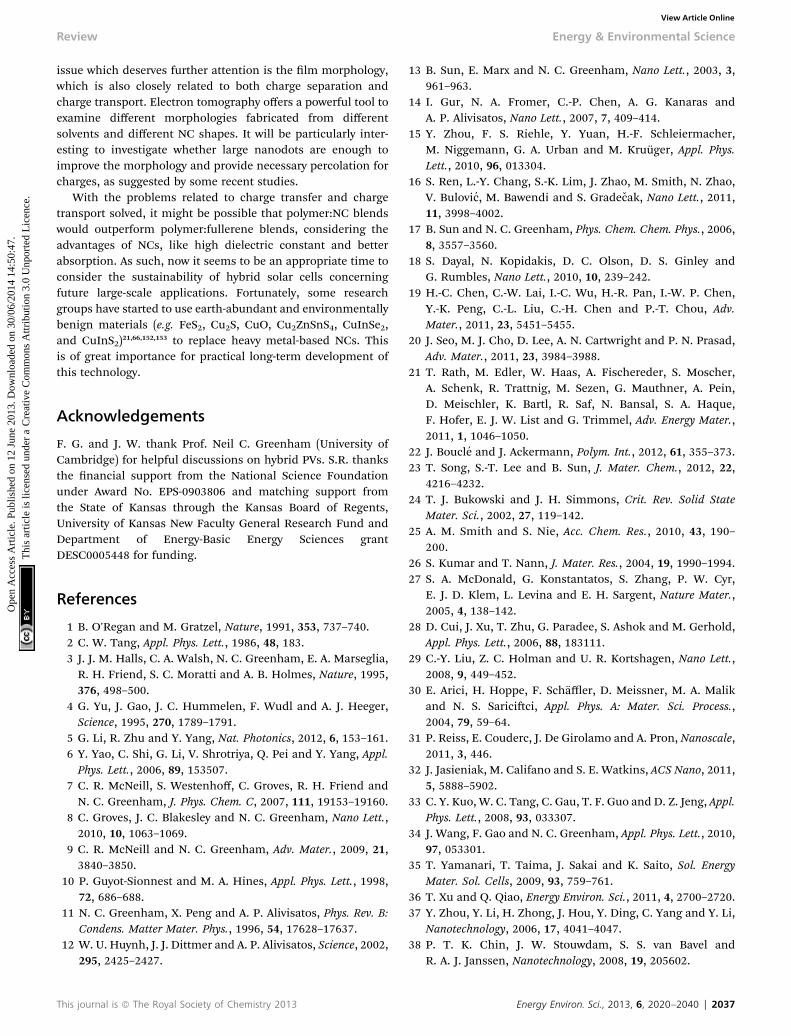
Review Energy & Environmental Science
Ope
n A
cces
s A
rtic
le. P
ublis
hed
on 1
2 Ju
ne 2
013.
Dow
nloa
ded
on 3
0/06
/201
4 14
:50:
47.
Thi
s ar
ticle
is li
cens
ed u
nder
a C
reat
ive
Com
mon
s A
ttrib
utio
n 3.
0 U
npor
ted
Lic
ence
.View Article Online
issue which deserves further attention is the lm morphology,which is also closely related to both charge separation andcharge transport. Electron tomography offers a powerful tool toexamine different morphologies fabricated from differentsolvents and different NC shapes. It will be particularly inter-esting to investigate whether large nanodots are enough toimprove the morphology and provide necessary percolation forcharges, as suggested by some recent studies.
With the problems related to charge transfer and chargetransport solved, it might be possible that polymer:NC blendswould outperform polymer:fullerene blends, considering theadvantages of NCs, like high dielectric constant and betterabsorption. As such, now it seems to be an appropriate time toconsider the sustainability of hybrid solar cells concerningfuture large-scale applications. Fortunately, some researchgroups have started to use earth-abundant and environmentallybenign materials (e.g. FeS2, Cu2S, CuO, Cu2ZnSnS4, CuInSe2,and CuInS2)21,66,152,153 to replace heavy metal-based NCs. Thisis of great importance for practical long-term development ofthis technology.
Acknowledgements
F. G. and J. W. thank Prof. Neil C. Greenham (University ofCambridge) for helpful discussions on hybrid PVs. S.R. thanksthe nancial support from the National Science Foundationunder Award No. EPS-0903806 and matching support fromthe State of Kansas through the Kansas Board of Regents,University of Kansas New Faculty General Research Fund andDepartment of Energy-Basic Energy Sciences grantDESC0005448 for funding.
References
1 B. O'Regan and M. Gratzel, Nature, 1991, 353, 737–740.2 C. W. Tang, Appl. Phys. Lett., 1986, 48, 183.3 J. J. M. Halls, C. A. Walsh, N. C. Greenham, E. A. Marseglia,R. H. Friend, S. C. Moratti and A. B. Holmes, Nature, 1995,376, 498–500.
4 G. Yu, J. Gao, J. C. Hummelen, F. Wudl and A. J. Heeger,Science, 1995, 270, 1789–1791.
5 G. Li, R. Zhu and Y. Yang, Nat. Photonics, 2012, 6, 153–161.6 Y. Yao, C. Shi, G. Li, V. Shrotriya, Q. Pei and Y. Yang, Appl.Phys. Lett., 2006, 89, 153507.
7 C. R. McNeill, S. Westenhoff, C. Groves, R. H. Friend andN. C. Greenham, J. Phys. Chem. C, 2007, 111, 19153–19160.
8 C. Groves, J. C. Blakesley and N. C. Greenham, Nano Lett.,2010, 10, 1063–1069.
9 C. R. McNeill and N. C. Greenham, Adv. Mater., 2009, 21,3840–3850.
10 P. Guyot-Sionnest and M. A. Hines, Appl. Phys. Lett., 1998,72, 686–688.
11 N. C. Greenham, X. Peng and A. P. Alivisatos, Phys. Rev. B:Condens. Matter Mater. Phys., 1996, 54, 17628–17637.
12 W. U. Huynh, J. J. Dittmer and A. P. Alivisatos, Science, 2002,295, 2425–2427.
This journal is ª The Royal Society of Chemistry 2013
13 B. Sun, E. Marx and N. C. Greenham, Nano Lett., 2003, 3,961–963.
14 I. Gur, N. A. Fromer, C.-P. Chen, A. G. Kanaras andA. P. Alivisatos, Nano Lett., 2007, 7, 409–414.
15 Y. Zhou, F. S. Riehle, Y. Yuan, H.-F. Schleiermacher,M. Niggemann, G. A. Urban and M. Kruuger, Appl. Phys.Lett., 2010, 96, 013304.
16 S. Ren, L.-Y. Chang, S.-K. Lim, J. Zhao, M. Smith, N. Zhao,V. Bulovic, M. Bawendi and S. Gradecak, Nano Lett., 2011,11, 3998–4002.
17 B. Sun and N. C. Greenham, Phys. Chem. Chem. Phys., 2006,8, 3557–3560.
18 S. Dayal, N. Kopidakis, D. C. Olson, D. S. Ginley andG. Rumbles, Nano Lett., 2010, 10, 239–242.
19 H.-C. Chen, C.-W. Lai, I.-C. Wu, H.-R. Pan, I.-W. P. Chen,Y.-K. Peng, C.-L. Liu, C.-H. Chen and P.-T. Chou, Adv.Mater., 2011, 23, 5451–5455.
20 J. Seo, M. J. Cho, D. Lee, A. N. Cartwright and P. N. Prasad,Adv. Mater., 2011, 23, 3984–3988.
21 T. Rath, M. Edler, W. Haas, A. Fischereder, S. Moscher,A. Schenk, R. Trattnig, M. Sezen, G. Mauthner, A. Pein,D. Meischler, K. Bartl, R. Saf, N. Bansal, S. A. Haque,F. Hofer, E. J. W. List and G. Trimmel, Adv. Energy Mater.,2011, 1, 1046–1050.
22 J. Boucle and J. Ackermann, Polym. Int., 2012, 61, 355–373.23 T. Song, S.-T. Lee and B. Sun, J. Mater. Chem., 2012, 22,
4216–4232.24 T. J. Bukowski and J. H. Simmons, Crit. Rev. Solid State
Mater. Sci., 2002, 27, 119–142.25 A. M. Smith and S. Nie, Acc. Chem. Res., 2010, 43, 190–
200.26 S. Kumar and T. Nann, J. Mater. Res., 2004, 19, 1990–1994.27 S. A. McDonald, G. Konstantatos, S. Zhang, P. W. Cyr,
E. J. D. Klem, L. Levina and E. H. Sargent, Nature Mater.,2005, 4, 138–142.
28 D. Cui, J. Xu, T. Zhu, G. Paradee, S. Ashok and M. Gerhold,Appl. Phys. Lett., 2006, 88, 183111.
29 C.-Y. Liu, Z. C. Holman and U. R. Kortshagen, Nano Lett.,2008, 9, 449–452.
30 E. Arici, H. Hoppe, F. Schaffler, D. Meissner, M. A. Malikand N. S. Saricici, Appl. Phys. A: Mater. Sci. Process.,2004, 79, 59–64.
31 P. Reiss, E. Couderc, J. De Girolamo and A. Pron, Nanoscale,2011, 3, 446.
32 J. Jasieniak, M. Califano and S. E. Watkins, ACS Nano, 2011,5, 5888–5902.
33 C. Y. Kuo, W. C. Tang, C. Gau, T. F. Guo and D. Z. Jeng, Appl.Phys. Lett., 2008, 93, 033307.
34 J. Wang, F. Gao and N. C. Greenham, Appl. Phys. Lett., 2010,97, 053301.
35 T. Yamanari, T. Taima, J. Sakai and K. Saito, Sol. EnergyMater. Sol. Cells, 2009, 93, 759–761.
36 T. Xu and Q. Qiao, Energy Environ. Sci., 2011, 4, 2700–2720.37 Y. Zhou, Y. Li, H. Zhong, J. Hou, Y. Ding, C. Yang and Y. Li,
Nanotechnology, 2006, 17, 4041–4047.38 P. T. K. Chin, J. W. Stouwdam, S. S. van Bavel and
R. A. J. Janssen, Nanotechnology, 2008, 19, 205602.
Energy Environ. Sci., 2013, 6, 2020–2040 | 2037

Energy & Environmental Science Review
Ope
n A
cces
s A
rtic
le. P
ublis
hed
on 1
2 Ju
ne 2
013.
Dow
nloa
ded
on 3
0/06
/201
4 14
:50:
47.
Thi
s ar
ticle
is li
cens
ed u
nder
a C
reat
ive
Com
mon
s A
ttrib
utio
n 3.
0 U
npor
ted
Lic
ence
.View Article Online
39 S. Zhang, P. W. Cyr, S. A. McDonald, G. Konstantatos andE. H. Sargent, Appl. Phys. Lett., 2005, 87, 233101.
40 A. A. R. Watt, D. Blake, J. H. Warner, E. A. Thomsen,E. L. Tavenner, H. Rubinsztein-Dunlop and P. Meredith,J. Phys. D: Appl. Phys., 2005, 38, 2006–2012.
41 K. M. Noone, E. Strein, N. C. Anderson, P.-T. Wu,S. A. Jenekhe and D. S. Ginger, Nano Lett., 2010, 10, 2635–2639.
42 D. Qi, M. Fischbein, M. Drndic and S. Selmic, Appl. Phys.Lett., 2005, 86, 093103.
43 X. Jiang, R. D. Schaller, S. B. Lee, J. M. Pietryga, V. I. Klimovand A. A. Zakhidov, J. Mater. Res., 2011, 22, 2204–2210.
44 Z. Tan, T. Zhu, M. Thein, S. Gao, A. Cheng, F. Zhang,C. Zhang, H. Su, J. Wang, R. Henderson, J. Hahm, Y. Yangand J. Xu, Appl. Phys. Lett., 2009, 95, 063510.
45 K. M. Noone, N. C. Anderson, N. E. Horwitz, A. M. Munro,A. P. Kulkarni and D. S. Ginger, ACS Nano, 2009, 3, 1345–1352.
46 R. Osterbacka, C. P. An, X. M. Jiang and Z. V. Vardeny,Science, 2000, 287, 839–842.
47 E. Strein, A. Colbert, S. Subramaniyan, H. Nagaoka,C. W. Schlenker, E. Janke, S. A. Jenekhe and D. S. Ginger,Energy Environ. Sci., 2013, 6, 769–775.
48 W. Ma, J. M. Luther, H. Zheng, Y. Wu and A. P. Alivisatos,Nano Lett., 2009, 9, 1699–1703.
49 R. Debnath, J. Tang, D. A. Barkhouse, X. Wang,A. G. Pattantyus-Abraham, L. Brzozowski, L. Levina andE. H. Sargent, J. Am. Chem. Soc., 2010, 132, 5952–5953.
50 W. Ma, S. L. Swisher, T. Ewers, J. Engel, V. E. Ferry,H. A. Atwater and A. P. Alivisatos, ACS Nano, 2011, 5,8140–8147.
51 R. Debnath, M. T. Greiner, I. J. Kramer, A. Fischer, J. Tang,D. A. R. Barkhouse, X. Wang, L. Levina, Z.-H. Lu andE. H. Sargent, Appl. Phys. Lett., 2010, 97, 023109.
52 J. Tang, K. W. Kemp, S. Hoogland, K. S. Jeong, H. Liu,L. Levina, M. Furukawa, X. Wang, R. Debnath, D. Cha,K. W. Chou, A. Fischer, A. Amassian, J. B. Asbury andE. H. Sargent, Nature Mater., 2011, 10, 765–771.
53 A. H. Ip, S. M. Thon, S. Hoogland, O. Voznyy,D. Zhitomirsky, R. Debnath, L. Levina, L. R. Rollny,G. H. Carey, A. Fischer, K. W. Kemp, I. J. Kramer, Z. Ning,A. J. Labelle, K. W. Chou, A. Amassian and E. H. Sargent,Nat. Nanotechnol., 2012, 7, 577–582.
54 E. H. Sargent, Nat. Photonics, 2012, 6, 133–135.55 A. Nozik, Phys. E, 2002, 14, 115–120.56 R. D. Schaller and V. I. Klimov, Phys. Rev. Lett., 2004, 92,
186601.57 R. J. Ellingson, M. C. Beard, J. C. Johnson, P. Yu, O. I. Micic,
A. J. Nozik, A. Shabaev and A. L. Efros, Nano Lett., 2005, 5,865–871.
58 M. C. Beard, A. G. Midgett, M. Law, O. E. Semonin,R. J. Ellingson and A. J. Nozik, Nano Lett., 2009, 9, 836–845.
59 O. E. Semonin, J. M. Luther, S. Choi, H.-Y. Chen, J. Gao,A. J. Nozik and M. C. Beard, Science, 2011, 334, 1530–1533.
60 B. Ehrler, M. W. B. Wilson, A. Rao, R. H. Friend andN. C. Greenham, Nano Lett., 2012, 12, 1053–1057.
2038 | Energy Environ. Sci., 2013, 6, 2020–2040
61 B. Ehrler, B. J. Walker, M. L. Bohm, M. W. B. Wilson,Y. Vaynzof, R. H. Friend and N. C. Greenham, Nat.Commun., 2012, 3, 1019.
62 M. B. Smith and J. Michl, Chem. Rev., 2010, 110, 6891–6936.63 W.-L. Chan, M. Ligges, A. Jailaubekov, L. Kaake, L. Miaja-
Avila and X.-Y. Zhu, Science, 2011, 334, 1541–1545.64 C.-Y. Liu, Z. C. Holman and U. R. Kortshagen, Adv. Funct.
Mater., 2010, 20, 2157–2164.65 B. Sun, G. Zou, X. Shen and X. Zhang, Appl. Phys. Lett., 2009,
94, 233504.66 Y. Yang, H. Zhong, Z. Bai, B. Zou, Y. Li and G. D. Scholes,
J. Phys. Chem. C, 2012, 116, 7280–7286.67 E. Arici, N. s. Saricici and D. Meissner, Adv. Funct. Mater.,
2003, 13, 165–171.68 S. Ren, N. Zhao, S. C. Crawford, M. Tambe, V. Bulovic and
S. Gradecak, Nano Lett., 2010, 11, 408–413.69 L. Wang, Y. Liu, X. Jiang, D. Qin and Y. Cao, J. Phys. Chem.
C, 2007, 111, 9538–9542.70 H.-C. Liao, S.-Y. Chen and D.-M. Liu, Macromolecules, 2009,
42, 6558–6563.71 W. J. E. Beek, M. M. Wienk and R. a. J. Janssen, Adv. Mater.,
2004, 16, 1009–1013.72 L. J. A. Koster, W. J. van Strien, W. J. E. Beek and
P. W. M. Blom, Adv. Funct. Mater., 2007, 17, 1297–1302.73 W. J. E. Beek, M. M. Wienk, M. Kemerink, X. Yang and
R. A. J. Janssen, J. Phys. Chem. B, 2005, 109, 9505–9516.74 W. J. E. Beek, M. M. Wienk and R. a. J. Janssen, Adv. Funct.
Mater., 2006, 16, 1112–1116.75 W. J. E. Beek, L. H. Slooff, M. M. Wienk, J. M. Kroon and
R. a. J. Janssen, Adv. Funct. Mater., 2005, 15, 1703–1707.76 S. D. Oosterhout, M. M. Wienk, S. S. van Bavel,
R. Thiedmann, L. Jan Anton Koster, J. Gilot, J. Loos,V. Schmidt and R. A. J. Janssen, Nature Mater., 2009, 8,818–824.
77 C. Y. Kwong, A. B. Djurisic, P. C. Chui, K. W. Cheng andW. K. Chan, Chem. Phys. Lett., 2004, 384, 372–375.
78 P. a. van Hal, M. m. Wienk, J. m. Kroon, W. j. h. Verhees,L. h. Slooff, W. j. h. van Gennip, P. Jonkheijm andR. a. j. Janssen, Adv. Mater., 2003, 15, 118–121.
79 L. H. Slooff, M. M. Wienk and J. M. Kroon, Thin Solid Films,2004, 451–452, 634–638.
80 J. Liu, W. Wang, H. Yu, Z. Wu, J. Peng and Y. Cao, Sol.Energy Mater. Sol. Cells, 2008, 92, 1403–1409.
81 Y.-Y. Lin, T.-H. Chu, C.-W. Chen and W.-F. Su, Appl. Phys.Lett., 2008, 92, 053312.
82 Y.-Y. Lin, T.-H. Chu, S.-S. Li, C.-H. Chuang, C.-H. Chang,W.-F. Su, C.-P. Chang, M.-W. Chu and C.-W. Chen, J. Am.Chem. Soc., 2009, 131, 3644–3649.
83 G. K. Mor, S. Kim, M. Paulose, O. K. Varghese, K. Shankar,J. Basham and C. A. Grimes, Nano Lett., 2009, 9, 4250–4257.
84 J. A. Chang, J. H. Rhee, S. H. Im, Y. H. Lee, H. Kim, S. I. Seok,M. K. Nazeeruddin and M. Gratzel, Nano Lett., 2010, 10,2609–2612.
85 W. Zhang, R. Zhu, F. Li, Q. Wang and B. Liu, J. Phys. Chem.C, 2011, 115, 7038–7043.
86 W. U. Huynh, X. Peng and A. P. Alivisatos, Adv. Mater., 1999,11, 923–927.
This journal is ª The Royal Society of Chemistry 2013

Review Energy & Environmental Science
Ope
n A
cces
s A
rtic
le. P
ublis
hed
on 1
2 Ju
ne 2
013.
Dow
nloa
ded
on 3
0/06
/201
4 14
:50:
47.
Thi
s ar
ticle
is li
cens
ed u
nder
a C
reat
ive
Com
mon
s A
ttrib
utio
n 3.
0 U
npor
ted
Lic
ence
.View Article Online
87 P. Wang, A. Abrusci, H. M. P. Wong, M. Svensson,M. R. Andersson and N. C. Greenham, Nano Lett., 2006, 6,1789–1793.
88 R. Kroon, M. Lenes, J. C. Hummelen, P. W. M. Blom andB. de Boer, Polym. Rev., 2008, 48, 531–582.
89 Y. Zhou, M. Eck, C. Veit, B. Zimmermann, F. Rauscher,P. Niyamakom, S. Yilmaz, I. Dumsch, S. Allard, U. Scherfand M. Kruger, Sol. Energy Mater. Sol. Cells, 2011, 95,1232–1237.
90 D. Celik, M. Kruger, C. Veit, H. F. Schleiermacher,B. Zimmermann, S. Allard, I. Dumsch, U. Scherf,F. Rauscher and P. Niyamakom, Sol. Energy Mater. Sol.Cells, 2012, 98, 433–440.
91 R. Zhou, Y. Zheng, L. Qian, Y. Yang, P. H. Holloway andJ. Xue, Nanoscale, 2012, 4, 3507–3514.
92 L. A. A. Pettersson, L. S. Roman and O. Inganas, J. Appl.Phys., 1999, 86, 487.
93 J. D. Myers, W. Cao, V. Cassidy, S.-H. Eom, R. Zhou, L. Yang,W. You and J. Xue, Energy Environ. Sci., 2012, 5, 6900–6904.
94 L. Qian, J. Yang, R. Zhou, A. Tang, Y. Zheng, T.-K. Tseng,D. Bera, J. Xue and P. H. Holloway, J. Mater. Chem., 2011,21, 3814.
95 J. Y. Kim, K. Lee, N. E. Coates, D. Moses, T.-Q. Nguyen,M. Dante and A. J. Heeger, Science, 2007, 317, 222–225.
96 J. Gilot, M. M. Wienk and R. A. J. Janssen, Appl. Phys. Lett.,2007, 90, 143512.
97 O. Hagemann, M. Bjerring, N. C. Nielsen and F. C. Krebs,Sol. Energy Mater. Sol. Cells, 2008, 92, 1327–1335.
98 J. Bredas, J. Cornil and A. J. Heeger, Adv. Mater., 1996, 8,447–452.
99 M. Muntwiler, Q. Yang, W. A. Tisdale and X.-Y. Zhu, Phys.Rev. Lett., 2008, 101, 196403.
100 P. W. M. Blom, V. D. Mihailetchi, L. J. A. Koster andD. E. Markov, Adv. Mater., 2007, 19, 1551–1566.
101 V. Choong, Y. Park, Y. Gao, T. Wehrmeister, K. Mullen,B. R. Hsieh and C. W. Tang, Appl. Phys. Lett., 1996, 69, 1492.
102 J. J. M. Halls, K. Pichler, R. H. Friend, S. C. Moratti andA. B. Holmes, Appl. Phys. Lett., 1996, 68, 3120.
103 T. Stubinger and W. Brutting, J. Appl. Phys., 2001, 90, 3632.104 L. Luer, H.-J. Egelhaaf, D. Oelkrug, G. Cerullo, G. Lanzani,
B.-H. Huisman and D. de Leeuw, Org. Electron., 2004, 5,83–89.
105 P. Peumans, A. Yakimov and S. R. Forrest, J. Appl. Phys.,2003, 93, 3693.
106 G. D. Scholes, Annu. Rev. Phys. Chem., 2003, 54, 57–87.107 W. U. Huynh, J. J. Dittmer, W. C. Libby, G. L. Whiting and
A. P. Alivisatos, Adv. Funct. Mater., 2003, 13, 73–79.108 J. D. Olson, G. P. Gray and S. A. Carter, Sol. Energy Mater.
Sol. Cells, 2009, 93, 519–523.109 J. Seo, W. J. Kim, S. J. Kim, K.-S. Lee, A. N. Cartwright and
P. N. Prasad, Appl. Phys. Lett., 2009, 94, 133302.110 E. J. D. Klem, D. D. MacNeil, P. W. Cyr, L. Levina and
E. H. Sargent, Appl. Phys. Lett., 2007, 90, 183113.111 J. M. Luther, M. Law, M. C. Beard, Q. Song, M. O. Reese,
R. J. Ellingson and A. J. Nozik, Nano Lett., 2008, 8, 3488–3492.
112 Y. Wu and G. Zhang, Nano Lett., 2010, 10, 1628–1631.
This journal is ª The Royal Society of Chemistry 2013
113 M. J. Greaney, S. Das, D. H. Webber, S. E. Bradforth andR. L. Brutchey, ACS Nano, 2012, 6, 4222–4230.
114 D. H. Webber and R. L. Brutchey, J. Am. Chem. Soc., 2011,134, 1085–1092.
115 J. Seo, S. J. Kim, W. J. Kim, R. Singh, M. Samoc,A. N. Cartwright and P. N. Prasad, Nanotechnology, 2009,20, 095202.
116 J. E. B. Katari, V. L. Colvin and A. P. Alivisatos, J. Phys.Chem., 1994, 98, 4109–4117.
117 M. Kuno, J. K. Lee, B. O. Dabbousi, F. V. Mikulec andM. G. Bawendi, J. Chem. Phys., 1997, 106, 9869–9882.
118 B. von Holt, S. Kudera, A. Weiss, T. E. Schrader, L. Manna,W. J. Parak and M. Braun, J. Mater. Chem., 2008, 18, 2728–2732.
119 I. Lokteva, N. Radychev, F. Witt, H. Borchert, J. Parisi andJ. Kolny-Olesiak, J. Phys. Chem. C, 2010, 114, 12784–12791.
120 N. Radychev, I. Lokteva, F. Witt, J. Kolny-Olesiak,H. Borchert and J. Parisi, J. Phys. Chem. C, 2011, 115,14111–14122.
121 M. Schadel, K. F. Jeltsch, P. Niyamakom, F. Rauscher,Y. Zhou, M. Kruger and K. Meerholz, J. Polym. Sci., Part B:Polym. Phys., 2012, 50, 75–82.
122 D. J. Milliron, A. P. Alivisatos, C. Pitois, C. Edder andJ. M. J. Frechet, Adv. Mater., 2003, 15, 58–61.
123 J. Locklin, D. Patton, S. Deng, A. Baba, M. Millan andR. C. Advincula, Chem. Mater., 2004, 16, 5187–5193.
124 Y.-C. Huang, J.-H. Hsu, Y.-C. Liao, W.-C. Yen, S.-S. Li,S.-T. Lin, C.-W. Chen and W.-F. Su, J. Mater. Chem., 2011,21, 4450.
125 J. Liu, T. Tanaka, K. Sivula, A. P. Alivisatos andJ. M. J. Frechet, J. Am. Chem. Soc., 2004, 126, 6550–6551.
126 S. D. Oosterhout, L. J. A. Koster, S. S. van Bavel, J. Loos,O. Stenzel, R. Thiedmann, V. Schmidt, B. Campo,T. J. Cleij, L. Lutzen, D. Vanderzande, M. M. Wienk andR. A. J. Janssen, Adv. Energy Mater., 2011, 1, 90–96.
127 S. S. van Bavel, E. Sourty, G. de With and J. Loos, Nano Lett.,2008, 9, 507–513.
128 A. L. Briseno, T. W. Holcombe, A. I. Boukai, E. C. Garnett,S. W. Shelton, J. J. M. Frechet and P. Yang, Nano Lett.,2009, 10, 334–340.
129 D. J. D. Moet, L. J. A. Koster, B. de Boer and P. W. M. Blom,Chem. Mater., 2007, 19, 5856–5861.
130 A. Watt, E. Thomsen, P. Meredith and H. Rubinsztein-Dunlop, Chem. Commun., 2004, 2334–2335.
131 A. A. R. Watt, P. Meredith, J. D. Riches, S. Atkinson andH. Rubinsztein-Dunlop, Curr. Appl. Phys., 2004, 4, 320–322.
132 H. C. Leventis, S. P. King, A. Sudlow, M. S. Hill, K. C. Molloyand S. A. Haque, Nano Lett., 2010, 10, 1253–1258.
133 S. Dowland, T. Lutz, A. Ward, S. P. King, A. Sudlow,M. S. Hill, K. C. Molloy and S. A. Haque, Adv. Mater.,2011, 23, 2739–2744.
134 C. Deibel and V. Dyakonov, Rep. Prog. Phys., 2010, 73,096401.
135 F. Gao, Z. Li, J. Wang, A. Rao, I. A. Howard, A. Abrusci,S. Massip, C. R. McNeill and N. C. Greenham, ACS Nano,submitted.
Energy Environ. Sci., 2013, 6, 2020–2040 | 2039

Energy & Environmental Science Review
Ope
n A
cces
s A
rtic
le. P
ublis
hed
on 1
2 Ju
ne 2
013.
Dow
nloa
ded
on 3
0/06
/201
4 14
:50:
47.
Thi
s ar
ticle
is li
cens
ed u
nder
a C
reat
ive
Com
mon
s A
ttrib
utio
n 3.
0 U
npor
ted
Lic
ence
.View Article Online
136 B. Sun, H. J. Snaith, A. S. Dhoot, S. Westenhoff andN. C. Greenham, J. Appl. Phys., 2005, 97, 014914.
137 L. Han, D. Qin, X. Jiang, Y. Liu, L. Wang, J. Chen and Y. Cao,Nanotechnology, 2006, 17, 4736–4742.
138 J. C. Hindson, Z. Saghi, J.-C. Hernandez-Garrido,P. A. Midgley and N. C. Greenham, Nano Lett., 2011, 11,904–909.
139 M.-C. Wu, C.-H. Chang, H.-H. Lo, Y.-S. Lin, Y.-Y. Lin,W.-C. Yen, W.-F. Su, Y.-F. Chen and C.-W. Chen, J. Mater.Chem., 2008, 18, 4097.
140 Y. Zhou, M. Eck, C. Men, F. Rauscher, P. Niyamakom,S. Yilmaz, I. Dumsch, S. Allard, U. Scherf and M. Kruger,Sol. Energy Mater. Sol. Cells, 2011, 95, 3227–3232.
141 K. F. Jeltsch, M. Schadel, J.-B. Bonekamp, P. Niyamakom,F. Rauscher, H. W. A. Lademann, I. Dumsch, S. Allard,U. Scherf and K. Meerholz, Adv. Funct. Mater., 2012, 22,397–404.
142 J. Yang, A. Tang, R. Zhou and J. Xue, Sol. Energy Mater. Sol.Cells, 2011, 95, 476–482.
143 A. Lefrançois, E. Couderc, J. Faure-Vincent, S. Sadki, A. Pronand P. Reiss, J. Mater. Chem., 2011, 21, 11524–11531.
144 J. A. Merlo and C. D. Frisbie, J. Polym. Sci., Part B: Polym.Phys., 2003, 41, 2674–2680.
2040 | Energy Environ. Sci., 2013, 6, 2020–2040
145 D. Ginger and N. Greenham, Phys. Rev. B: Condens. MatterMater. Phys., 1999, 59, 10622–10629.
146 M. D. Heinemann, K. von Maydell, F. Zutz, J. Kolny-Olesiak,H. Borchert, I. Riedel and J. Parisi, Adv. Funct. Mater., 2009,19, 3788–3795.
147 J. Albero, Y. Zhou, M. Eck, F. Rauscher, P. Niyamakom,I. Dumsch, S. Allard, U. Scherf, M. Kruger andE. Palomares, Chem. Sci., 2011, 2, 2396–2401.
148 J. Albero, E. Martınez-Ferrero, J. Ajuria, C. Waldauf,R. Pacios and E. Palomares, Phys. Chem. Chem. Phys.,2009, 11, 9644–9647.
149 G. Grancini, M. Biasiucci, R. Mastria, F. Scotognella,F. Tassone, D. Polli, G. Gigli and G. Lanzani, J. Phys.Chem. Lett., 2012, 3, 517–523.
150 Z. Li, F. Gao, N. C. Greenham and C. R. McNeill, Adv. Funct.Mater., 2011, 21, 1419–1431.
151 K. M. Noone, S. Subramaniyan, Q. Zhang, G. Cao,S. A. Jenekhe and D. S. Ginger, J. Phys. Chem. C, 2011,115, 24403–24410.
152 A. Kirkeminde, B. A. Ruzicka, R. Wang, S. Puna, H. Zhaoand S. Ren, ACS Appl. Mater. Interfaces, 2012, 4, 1174–1177.
153 M. Gong, A. Kirkeminde, Y. Xie, R. Lu, J. Liu, J. Z. Wu andS. Ren, Adv. Opt. Mater., 2013, 1, 78–83.
This journal is ª The Royal Society of Chemistry 2013