The OIF Compliant Tunable Laser MSA - … · REFERENCE DOCUMENT FOR OIF COMPLIANT TUNABLE LASER...
120
REFERENCE DOCUMENT FOR OIF COMPLIANT TUNABLE LASER MODULE MSA No changes are allowed to this document A printed version of this document is an uncontrolled copy Public Document Release PV:1.2.3 Page 1 of 120 Date: 14 July 2003 The OIF Compliant Tunable Laser MSA This document has been created by the OIF COMPLIANT TUNABLE LASER MSA GROUP and is offered to tunable laser module users and suppliers as a basis for a technical agreement. It is not a warranted document. Each tunable laser supplier will have their own data sheet. If the tunable laser module user wishes to find a warranted document, they should consult the datasheet of the chosen tunable laser module supplier. The MSA group reserves the right at any time to add, amend or withdraw technical data contained in this document MSA Group Contacts Company Contact Email Address iolon Jeff Hutchins [email protected] Santur Jay Kubicky [email protected] Intel Raj Batra [email protected] Bookham Technologies Timothy Simmons [email protected] Princeton Optronics Timothy Hayes [email protected] Agility Kevin Affolter [email protected] Document Version: PV:1.2.3 http://TunableLaserMSA.com No license, express or implied, by estoppel or otherwise, to any intellectual property rights of any MSA member (defined for the purposes of this paragraph as the companies who support the MSA Tunable Laser document or "MSA") is granted by virtue of this website or the MSA. Furthermore, except as provided in the terms and conditions of sale of any products designed to comply with the MSA, no MSA member assumes any liability whatsoever, to any third party including other MSA members, and specifically disclaims any express or implied warranty, relating to the use or reliance upon the MSA for any purposes whatsoever, including without limitation, (i) the design, development, manufacture, marketing or sale of any product designed to comply with the MSA or support MSA-compliant products, (ii) liability or warranties relating to fitness for a particular purpose, merchantability, or infringement of any patent, copyright or other intellectual property right, and (iii) errors or omissions in the MSA. The MSA is not intended to be used to design, develop, manufacture, market or sell any products intended for use in medical, life-saving, or life-sustaining applications. The MSA members may make changes to the MSA at any time, without notice.
-
Upload
hoangthien -
Category
Documents
-
view
216 -
download
2
Transcript of The OIF Compliant Tunable Laser MSA - … · REFERENCE DOCUMENT FOR OIF COMPLIANT TUNABLE LASER...

REFERENCE DOCUMENT FOR OIF COMPLIANT TUNABLE LASER MODULE MSA No changes are allowed to this document
A printed version of this document is an uncontrolled copy
Public Document Release PV:1.2.3 Page 1 of 120 Date: 14 July 2003
The OIF Compliant Tunable Laser MSA This document has been created by the OIF COMPLIANT TUNABLE LASER MSA GROUP and is offered to tunable laser module users and suppliers as a basis for a technical agreement. It is not a warranted document. Each tunable laser supplier will have their own data sheet. If the tunable laser module user wishes to find a warranted document, they should consult the datasheet of the chosen tunable laser module supplier. The MSA group reserves the right at any time to add, amend or withdraw technical data contained in this document MSA Group Contacts
Company Contact Email Address iolon Jeff Hutchins [email protected] Santur Jay Kubicky [email protected] Intel Raj Batra [email protected] Bookham Technologies Timothy Simmons [email protected] Princeton Optronics Timothy Hayes [email protected] Agility Kevin Affolter [email protected]
Document Version: PV:1.2.3
http://TunableLaserMSA.com
No license, express or implied, by estoppel or otherwise, to any intellectual property rights of any MSA member (defined for the purposes of this paragraph as the companies who support the MSA Tunable Laser document or "MSA") is granted by virtue of this website or the MSA. Furthermore, except as provided in the terms and conditions of sale of any products designed to comply with the MSA, no MSA member assumes any liability whatsoever, to any third party including other MSA members, and specifically disclaims any express or implied warranty, relating to the use or reliance upon the MSA for any purposes whatsoever, including without limitation, (i) the design, development, manufacture, marketing or sale of any product designed to comply with the MSA or support MSA-compliant products, (ii) liability or warranties relating to fitness for a particular purpose, merchantability, or infringement of any patent, copyright or other intellectual property right, and (iii) errors or omissions in the MSA. The MSA is not intended to be used to design, develop, manufacture, market or sell any products intended for use in medical, life-saving, or life-sustaining applications. The MSA members may make changes to the MSA at any time, without notice.

REFERENCE DOCUMENT FOR OIF COMPLIANT TUNABLE LASER MODULE MSA No changes are allowed to this document
A printed version of this document is an uncontrolled copy
Public Document Release PV:1.2.3 Page 2 of 120 Date: 14 July 2003
1 Contents of The OIF Compliant Tunable Laser MSA
1.1 Table of Contents
The OIF Compliant Tunable Laser MSA ......................................................................................... 1 1 Contents of The OIF Compliant Tunable Laser MSA............................................................... 2
1.1 Table of Contents.............................................................................................................. 2 1.2 List of Tables..................................................................................................................... 4 1.3 List of Figures.................................................................................................................... 5 1.4 Document Revision History............................................................................................... 5
2 References ............................................................................................................................... 6 2.1 External Reference Documents ........................................................................................ 6 2.2 Conventions Used in This Document................................................................................ 6
3 Introduction The OIF Tunable Laser MSA-IA........................................................................... 8 3.1 Scope ................................................................................................................................ 8 3.2 Objectives ......................................................................................................................... 8 3.3 Background ....................................................................................................................... 8 3.4 Design Objectives and Features..................................................................................... 10 3.5 Communication Overview ............................................................................................... 11
3.5.1 Physical Interfaces................................................................................................... 12 3.6 Command Overview........................................................................................................ 12
3.6.1 Command Execution Overlap.................................................................................. 13 3.6.2 Extended Addressing............................................................................................... 13 3.6.3 Data Types............................................................................................................... 14
3.6.3.1 Two Byte Data Values ...................................................................................... 14 3.6.3.2 Multi-byte Fields................................................................................................ 15
3.6.4 Execution Error Field Conditions ............................................................................. 15 3.7 Command & Module Features ........................................................................................ 15
3.7.1 Module Reset........................................................................................................... 15 3.7.2 Register Lockout for Write Access........................................................................... 15 3.7.3 Communication Error Detection............................................................................... 16
3.7.3.1 Detection by Module......................................................................................... 16 3.7.3.2 Detection by Host ............................................................................................. 16
3.7.4 Execution Error Detection........................................................................................ 16 3.7.5 Module Signaling Lines............................................................................................ 16 3.7.6 Non-Volatile Default Configuration .......................................................................... 17
4 Physical Layer & Electrical Characteristics ............................................................................ 18 4.1 Module Electrical Interface.............................................................................................. 18
4.1.1 Electrical Connector................................................................................................. 18 4.1.2 Pin Assignments ...................................................................................................... 18 4.1.3 Electrical Characteristics.......................................................................................... 24
4.2 Communication Interfaces .............................................................................................. 25 4.2.1 RS232 Communications Interface ........................................................................... 27 4.2.2 SPI Communications Interface ................................................................................ 31 4.2.3 I2C Communications Interface ................................................................................. 36
5 Transport Layer ...................................................................................................................... 43 5.1 Overview ......................................................................................................................... 43 5.2 Checksum ....................................................................................................................... 43

REFERENCE DOCUMENT FOR OIF COMPLIANT TUNABLE LASER MODULE MSA No changes are allowed to this document
A printed version of this document is an uncontrolled copy
Public Document Release PV:1.2.3 Page 3 of 120 Date: 14 July 2003
5.3 CRC-16 ........................................................................................................................... 44 5.4 Packet Pacing ................................................................................................................. 45
6 Command Interface (Application Layer)................................................................................. 47 6.1 Command Format ........................................................................................................... 47
6.1.1 In-Bound (Host to Module)....................................................................................... 47 6.1.2 Out-Bound (Module to Host).................................................................................... 47
6.2 Register Summary .......................................................................................................... 49 6.3 Command Description Format ........................................................................................ 52 6.4 Generic Module Commands ........................................................................................... 54
6.4.1 NOP/Status (NOP 0x00) [RW]................................................................................. 54 6.4.2 Device Type (DevTyp 0x01) [R]............................................................................... 55 6.4.3 Manufacturer (MFGR 0x02) [R] ............................................................................... 56 6.4.4 Model (Model 0x03) [R]............................................................................................ 57 6.4.5 Serial Number (SerNo 0x04) [R].............................................................................. 58 6.4.6 Manufacturing Date (MFGDate0x05) [R] ................................................................. 58 6.4.7 Release (Release 0x06) [R]..................................................................................... 59 6.4.8 Release Backwards Compatibility (RelBack 0x07) [R] ............................................ 61 6.4.9 General Module Configuration (GenCfg 0x08) [RW] ............................................... 62 6.4.10 IO Capabilities (IOCap 0x0D) [RW] ......................................................................... 63 6.4.11 Extended Addressing Mode Registers (0x09-0x0B, 0x0E-0x10) [RW] ................... 65
6.4.11.1 Extended Address Configuration (EAC 0x09 & 0x0E) ..................................... 66 6.4.11.2 Extended Address (EA 0x0A & 0x0F) .............................................................. 67 6.4.11.3 Extended Address Access Register (EAR 0x0B & 0x10)................................. 67
6.4.12 Assert CRC (WCRC 0x11) [W] ................................................................................ 68 6.4.13 Read CRC (RCRC 0x12) [R] ................................................................................... 69 6.4.14 Last Response (LstResp 0x13) [R]........................................................................ 70 6.4.15 Download Configuration (DLConfig 0x14) [RW] ...................................................... 71 6.4.16 Download Status (DLStatus 0x15) [R] ..................................................................... 74 6.4.17 Register Lockout (Lock 0x16) [RW] ......................................................................... 75
6.5 Module Status Commands.............................................................................................. 77 6.5.1 StatusF, StatusW (0x20, 0x21) [RW]....................................................................... 77 6.5.2 Power Threshold (FPowTh, WPowTh 0x22, 0x23) [RW] ........................................ 81 6.5.3 Frequency Threshold (FFreqTh, WFreqTh 0x24, 0x25) [RW]................................. 82 6.5.4 Thermal Threshold (FThermTh, WThermTh 0x26, 0x27) [RW]............................... 83 6.5.5 SRQ* Triggers (SRQT 0x28) [RW] .......................................................................... 84 6.5.6 FATAL* Triggers (FatalT 0x29) [RW]....................................................................... 85 6.5.7 ALM* Triggers (ALMT 0x2A) [RW]........................................................................... 86
6.6 Module Optical Settings .................................................................................................. 88 6.6.1 Channel (Channel 0x30) [RW]................................................................................. 88 6.6.2 Optical Power Set Point (PWR 0x31) [RW] ............................................................. 90 6.6.3 Reset/Enable (ResEna 0x32) [RW] ......................................................................... 91 6.6.4 Module Configuration Behavior (MCB 0x33) [RW] .................................................. 93 6.6.5 Grid Spacing (Grid 0x34) [RW] ................................................................................ 94 6.6.6 First Channel’s Frequency (FCF1, FCF2 0x35 – 0x36) [RW].................................. 95 6.6.7 Laser Frequency (LF1, LF2 0x40 – 0x41) [R].......................................................... 96 6.6.8 Optical Output Power (OOP 0x42) [R]..................................................................... 97 6.6.9 Current Temperature (CTemp 0x43) [R].................................................................. 97
6.7 Module’s Capabilities ...................................................................................................... 98 6.7.1 Optical Power Min/Max Set Points (OPSL, OPSH 0x50 – 0x51) [R]....................... 98 6.7.2 Laser’s First/Last Frequency (LFL1/2, LFH1/2 0x52-0x55) [R] ............................... 99 6.7.3 Laser’s Minimum Grid Spacing (LGrid 0x56)......................................................... 100
6.8 MSA Commands ........................................................................................................... 101
REFERENCE DOCUMENT FOR OIF COMPLIANT TUNABLE LASER MODULE MSA No changes are allowed to this document
A printed version of this document is an uncontrolled copy
Public Document Release PV:1.2.3 Page 4 of 120 Date: 14 July 2003
6.8.1 Module Currents (Currents 0x57) [R]..................................................................... 101 6.8.2 Module Temperatures (Temps 0x58) [R]............................................................... 102 6.8.3 Analog & Digital Dither (Dither(E,R,A,F) 0x59-0x5C) [RW] [Optional] ................. 103 6.8.4 TCase Warning Limits (TCaseL, TCaseH 0x5D, 0x5E) [RW] .............................. 105
6.9 Manufacturer Specific (0x80-0xFE) .............................................................................. 106 6.9.1 User Data Storage (User1 0xFF)........................................................................... 106
7 Optical Specifications ........................................................................................................... 107 7.1 Optical Characteristics .................................................................................................. 107
7.1.1 Optical Parameter Definitions ................................................................................ 107 7.1.1.1 Spectral Linewidth .......................................................................................... 107 7.1.1.2 SMSR (Side Mode Suppression Ratio) .......................................................... 107 7.1.1.3 RIN (Relative Intensity Noise) ........................................................................ 107
7.1.2 Application Requirement 1 (Ultra Long Haul) ........................................................ 108 7.1.3 Application Requirement 2 (Long Haul)................................................................. 109 7.1.4 Application Requirement 3 (Metro) ........................................................................ 110
7.2 Timing Specifications .................................................................................................... 111 7.3 Module Warm Up Time ................................................................................................. 111
8 Mechanical Specifications .................................................................................................... 112 8.1 Module Mechanical Outline Dimensions....................................................................... 112
9 Index..................................................................................................................................... 114 1.2 List of Tables Table 3.3-1: List of Contributors to the OIF-TL-01.1 Document...................................................... 9 Table 3.3-2: List of Contributors to the OIF-TLMSA-01.0 Document .............................................. 9 Table 3.6-1: Example Reading Module Status.............................................................................. 12 Table 3.6-2: Extended Address Register Description ................................................................... 13 Table 3.6-3: Extended Address Register READ Example ............................................................ 14 Table 3.6-4: Extended Address Register WRITE Example........................................................... 14 Table 3.7.2-1: Register Lockout Lock Levels ................................................................................ 16 Table 4-1 Pin Functions................................................................................................................. 18 Table 4.1-1 Pin Assignments......................................................................................................... 19 Table 4.1-2 Pin Functions.............................................................................................................. 20 Table 4.1-3: Electrical Characteristics........................................................................................... 24 Table 4.1-4: Absolute Maximum Ratings ...................................................................................... 24 Table 4.2-1: Physical Interface Selection ...................................................................................... 25 Table 4.2-2: Communication Interface Performance..................................................................... 25 Table 4.2-3: Communication Byte Numbering .............................................................................. 26 Table 4.2-4 RS232 Physical Interface Pins................................................................................... 27 Table 4.2-5 SPI Physical Interface Pin Table............................................................................... 31 Table 4.2-6 SPI Physical Interface Pin Timing ............................................................................. 35 Table 4.2-7 I2C-Bus Physical Interface Pin Table ......................................................................... 40 Table 5.3-1: CRC-16 Example ...................................................................................................... 45 Table 6.1-1: Packet Status Flags .................................................................................................. 48 Table 6.2-1: Table of Registers (Commands) ............................................................................... 49 Table 6.4-1 Extended Address Space Mode Selection (EAM) ..................................................... 67 Table 6.4.15-1 Firmware Download Example ............................................................................... 71 Table 6.4.15-2 Firmware Upload Example.................................................................................... 72 Table 6.4-3: Register Lockout Lock Levels ................................................................................... 76 Table 7-1: Optical Specification Requirement Matrix .................................................................. 107 Table 7.1.2-1: Optical Specifications (Application 1)................................................................... 108 Table 7.1.3-1: Optical Specifications (Application 2)................................................................... 109

REFERENCE DOCUMENT FOR OIF COMPLIANT TUNABLE LASER MODULE MSA No changes are allowed to this document
A printed version of this document is an uncontrolled copy
Public Document Release PV:1.2.3 Page 5 of 120 Date: 14 July 2003
Table 7.1.4-1: Optical Specifications (Application 3).................................................................. 110 Table 7.2-1: Timing Specifications .............................................................................................. 111 Table 7.3-1: Module Warm Up Time ........................................................................................... 111 1.3 List of Figures Figure 3.5-1– Three Layer Communication Diagram.................................................................... 11 Figure 3.6-1: Paradigms for Module Control ................................................................................. 12 Figure 4.1-1 Connector Pin Numbering......................................................................................... 18 Figure 4.2-1 RS232 Timing ........................................................................................................... 28 Figure 4.2-2 RS232 Communication or Execution Error Timing ................................................... 28 Figure 4.2-3 Alarm Timing ............................................................................................................. 29 Figure 4.2-4 SPI IOCLK Timing..................................................................................................... 31 Figure 4.2-5 SPI Read (or Write) Timing, 1 Byte Host .................................................................. 33 Figure 4.2-6 SPI Error Timing (Execution or Communication)...................................................... 33 Figure 4.2-7 SPI Transfer Timing .................................................................................................. 35 Figure 4.2-8 Connection of Standard and Fast mode devices to the I2C-Bus. ............................ 37 Figure 4.2-9 Bit transfer on the I2C-Bus ........................................................................................ 37 Figure 4.2-10 Start and Stop conditions........................................................................................ 37 Figure 4.2-11 Data Transfer on the I2C-Bus.................................................................................. 38 Figure 4.2-12 Acknowledge on the I2C-Bus .................................................................................. 39 Figure 4.2-13 A complete data transfer. ........................................................................................ 39 Figure 5.1-1: In-Bound (Host to Module) Frame ........................................................................... 43 Figure 5.1-2 Out-Bound (Module to Host) Frame.......................................................................... 43 Figure 5.1-3 Transport Layer Field Definitions .............................................................................. 43 Figure 5.4-1 Packet Pacing Example ............................................................................................ 46 Figure 8.1-1 Mechanical Outline Dimensions.............................................................................. 112 1.4 Document Revision History
Version Date Description Public Release V 1.1.1
25 Apr 2003 Jeff Hutchins Based upon OIF-TL-01.1
Public Release V 1.2.1 30 May 2003 Jeff Hutchins Based upon OIF-TLMSA-01.0
Public Release V 1.2.2 27 June 2003 Jeff Hutchins Fixed typo on FW versions so that they are consistent naming for RUNV and TYPE fields. (Use A1, A2, B1, B2) instead of 1,2,A,B
Public Release V 1.2.3 14 July 2003 Jeff Hutchins Fixed power command typos. Made table in §6.2 consistent with the power command documentation. Commands affected are FPowTh, WpowTh, PWR, OOP, OPSL, OPSH.

REFERENCE DOCUMENT FOR OIF COMPLIANT TUNABLE LASER MODULE MSA No changes are allowed to this document
A printed version of this document is an uncontrolled copy
Public Document Release PV:1.2.3 Page 6 of 120 Date: 14 July 2003
2 References 2.1 External Reference Documents The following documents should be read in conjunction with this specification OIF TL 01.1 OIF Tunable Laser Implementation Agreement
(www.oiforum.com) GR-468 CORE General Reliability Assurance Requirements for Optoelectronic
Devices Used in Telecommunications Equipment CENELEC. EN50081-1 Electromagnetic Compatibility – Generic Emissions Standard
part 1: Residential, Commercial and Light Industry CENELEC. EN50082-1 Electromagnetic Compatibility – Generic Immunity Standard part
1: Residential, Commercial and Light Industry CENELEC. EN50081-1 Electromagnetic Compatibility – Generic Emissions Standard
part 2: Residential, Commercial and Light Industry Philips 9397-750-00954 The I2C Bus specification (January 2000) EIA RS-232D The RS232 Bus Specification 21CFR 1040.10 Laser Safety IEC 60825-1 Safety Of Laser Products Part1: Equipment Classification,
Requirements and Users Guide ITU-T G692 Optical Interfaces For Multi-channel Systems with Optical
Amplifiers 2.2 Conventions Used in This Document
Numeric Values:
5, 05 Decimal 0x05 Hexadecimal
Bit Numbering Bit 0 is LSB1
Data Types Unsigned short int 16 bit, big endian Signed short int 15 bit + 1, two’s complement, big endian Character 7-bit ASCII character (0x00 to 0x7F) (\0 is the null character) Printable character (0x20 to 0x7E) String (ASCII) All strings are null terminated string (first character bits are 15:8)
Data Direction Out-bound Module to host transfer (Response packet)
1 LSB: Least significant bit

REFERENCE DOCUMENT FOR OIF COMPLIANT TUNABLE LASER MODULE MSA No changes are allowed to this document
A printed version of this document is an uncontrolled copy
Public Document Release PV:1.2.3 Page 7 of 120 Date: 14 July 2003
In-bound Host to module transfer (Command from host)

REFERENCE DOCUMENT FOR OIF COMPLIANT TUNABLE LASER MODULE MSA No changes are allowed to this document
A printed version of this document is an uncontrolled copy
Public Document Release PV:1.2.3 Page 8 of 120 Date: 14 July 2003
3 Introduction The OIF Tunable Laser MSA-IA 3.1 Scope
This document is a Multi-Source Agreement for tunable laser modules. It details a communication protocol, electrical interface, power supply, and optical specifications for use in telecommunications equipment operating in the C or L band. Mechanical form factors are also defined.
3.2 Objectives
The aim of this document is to form the basis for highly extensible performance agreements among tunable device manufacturers that, in addition to their individual contents, conform to this document. It recognizes that customers require the same communication protocol, electrical interface, power supply and mechanical form factor for tunable laser modules as well as a basic set of minimum optical performance requirements. The OIF Tunable Laser MSA is compliant with the OIF’s Tunable Laser Implementation Agreements (OIF-IAs) and contains several of the anticipated extensions to the OIF-IA.
3.3 Background
The OIF has completed two tunable laser projects. The first project resulted in the Tunable Laser Implementation Agreement, OIF-TL-01.1 began in April 2001 and was released in November 2002. A large number of contributors from a wide variety of consumers and suppliers of tunable lasers were involved in contributing and reviewing the first Implementation Agreement. (See Table 3.3-1) It addressed the communication protocol, electrical interface and mechanical form factor interoperability for tunable continuous wavelength (CW) lasers. The document serves as a roadmap for future tunable device implementation agreements. In February 2003, the OIF began a new fast track project, the Tunable Laser MSA Implementation Agreement. The contributors are shown in Table 3.3-2. This MSA-IA builds upon the existing Tunable Laser Implementation Agreement, generating a more comprehensive specification of the optical, electrical, mechanical, and communication protocols. It was completed in May 2003.

REFERENCE DOCUMENT FOR OIF COMPLIANT TUNABLE LASER MODULE MSA No changes are allowed to this document
A printed version of this document is an uncontrolled copy
Public Document Release PV:1.2.3 Page 9 of 120 Date: 14 July 2003
Table 3.3-1: List of Contributors to the OIF-TL-01.1 Document Name: Company: Name: Company: John Marchionda ADC Jeff Hutchins iolon Mike Peppler Agere Systems Eric Selvik Iolon Sean Hannam Agere Systems Angel Molina Lucent James Moffat Agere Systems Shuai Shen Lucent Rang-Chen Yu Agility Communications George Pontis New Focus Stephen Scott Agility Communications Jose Downes Nortel Jim Blair AMCC Todd Stewart Nortel Charles Duvall Bandwidth9 Peter Dartnell Nortel Yuan Li Blue Sky Research Larry McAdams Picarro Tim Simmons Bookham Technologies Steffen Koehler Sparkolor Larry Davis Ciena Jay Kubicky Santur Jay Lofthouse-Zeis Coherent Wes Stalcup Texas Instruments David Young Corvis Sinthia Khan Texas Instruments Raj Batra Intel
Table 3.3-2: List of Contributors to the OIF-TLMSA-01.0 Document
Name: Company: Name: Company: Kevin Affolter Agility Communications Ken Koller Intel Tim Simmons Bookham Jeff Hutchins iolon Richard Barlow Bookham Shuai Shen Lucent Diego Marchese Cisco Tim Hayes Princeton Optronics David Young Corvis Jay Kubicky Santur Raj Batra Intel Colin Chipman Santur
The OIF-IAs can be found at www.oiforum.com as document OIF-TL-01.1.pdf at http://www.oiforum.com/public/documents/OIF-TL-01.1.pdf and OIF-TLMSA-01.0.pdf at http://www.oiforum.com/public/documents/OIF-TLMSA-01.0.pdf.

REFERENCE DOCUMENT FOR OIF COMPLIANT TUNABLE LASER MODULE MSA No changes are allowed to this document
A printed version of this document is an uncontrolled copy
Public Document Release PV:1.2.3 Page 10 of 120 Date: 14 July 2003
3.4 Design Objectives and Features The OIF-IAs were created with the following design guidelines in mind.
o Configurable: The tunable laser’s behavior shall be configurable such that it can be used in a number of different network equipment manufacturer’s line card architectures and design philosophies.
Some examples: Three physical interface options are provided: I2C, RS232, SPI Alarms and service request behaviors are configurable as to
trigger conditions as well as latching/non-latching behavior. Module reset on power on condition is configurable.
o Efficient and Robust Communication Interface:
The command interface shall be robust and consume a relatively small fraction of the bus bandwidth. This allows interfaces such as 9600 baud RS232 to provide timely control of the module in the event of a SONET/SDH protection switch. The efficient interface also provides for high bus utilization for highly shared busses such as SPI and I2C. Some examples:
The command interface consists of only 4 bytes per command. For instance, ~4ms is required to send a set channel command over RS232 and ~8us for a relatively pedestrian 4Mb/s SPI interface. Many other command interfaces require 7 or more bytes to transmit the same command.
The interface keeps all communications transactions relatively short such that commands can be interlaced. For example, a SONET/SDH protection event can be handled in a timely manner while the module’s firmware is being uploaded.
o Extensible Platform for Communication Interfaces:
The OIF-IA communication protocol is designed around 3 independent layers: Physical Layer: There are 3 physical interfaces to choose from. (I2C, RS232, SPI)
Transport Layer: Reliable data exchange (framing, checksums and error reporting, pacing)
Application Layer: General and specific commands
These features allow other tunable devices (such as tunable transmitters or receivers) to use the same protocol. The application layer’s command set has been divided into two groupings:
The first group of commands deals with general module behavior as well as providing a way to determine what kind of module is present (tunable laser, tunable transmitter, etc.).
The second group of commands is device type specific. This document describes the “CW Laser” device type.
The application layer also provides the ability to registers hold two object types: either 16 bit integers or an arbitrarily long sequence of bytes (multi-byte response). The command response identifies the response as either a 16-bit integer or multi-byte response.

REFERENCE DOCUMENT FOR OIF COMPLIANT TUNABLE LASER MODULE MSA No changes are allowed to this document
A printed version of this document is an uncontrolled copy
Public Document Release PV:1.2.3 Page 11 of 120 Date: 14 July 2003
3.5 Communication Overview
The following diagram (Figure 3.5-1) depicts the communication process.
Figure 3.5-1– Three Layer Communication Diagram
Assume the host has a request to transmit to the module (Host’s Request). The request is first encoded as a 28-bit command packet in the Host Driver’s application layer. The command is then framed as a 32-bit packet in the host driver’s transport layer. The framing operation includes the addition of a BIP-42 checksum. Finally, the host driver’s physical interface (RS232 shown) encodes the 32 bit packet as 4 ten bit3 RS232 “characters” and transmits in across the TxD line to the module. The module’s physical layer receives 40 bits and de-codes them by removing the RS232 start and stop bits. The resulting 32-bit frame is delivered to the transport layer where checksum is checked for consistency. Assuming no error is generated, the 28-bit command packet is delivered to the module’s application layer where the command is decoded and executed. The command execution will generate a response when complete4. The response packet consists of 26 bits. The response packet is delivered to the module’s transport layer which frames the packet by pre-pending a checksum, communication error (CE), and a response flag. The resulting
2 Bit Interleaved Parity (4 bits) 3 Note each byte to be transmitted by RS232 is encapsulated by a start and stop bit thus pre-pending 1 bit and post-pending 1 bit for a total of 10 bits for each byte to be transmitted. 4 Note that an initial response may also be generated for commands whose execution time exceeds the command response timeout period. The host can either poll for completion of the command or have pre-configured the module to issue a service request (SRQ) upon completion of the command.

REFERENCE DOCUMENT FOR OIF COMPLIANT TUNABLE LASER MODULE MSA No changes are allowed to this document
A printed version of this document is an uncontrolled copy
Public Document Release PV:1.2.3 Page 12 of 120 Date: 14 July 2003
32-bit packet is then delivered to the module’s physical layer where it is then encoded as 40 bits. The host then receives the 4 RS232 characters and performs the inverse operations as the packet moves up the host’s layer hierarchy.
3.5.1 Physical Interfaces The communications interface supports three physical layer protocols
I2C RS232 SPI
The interface to be used is determined at power up or hard reset by the state of the IOMode and IOMode1 pins (see §4.2) for the tunable laser module. Note that for a given application, the manufacturer need only implement the physical interface required by the user application.
3.6 Command Overview
The commands to the module consist of a 9-bit operation followed by 2 bytes of optional data. Alternatively, the command can be thought of as one read/write bit followed by an 8-bit register number followed by 2 bytes of optional data. See Figure 3.6-1. The register paradigm will be used in this document.
Figure 3.6-1: Paradigms for Module Control
Command Paradigm 9 bit command Data byte 1 Data byte 2
Register Paradigm Read/Write Bit 8 bit register number Data byte 1 Data byte 2
There are 256 directly accessible registers (0x00 to 0xFF) in the primary register address space. The OIF-IA allocates the first 32 registers (0x00 to 0x1F) for generic module operations for all module types. Another 96 registers (0x20-0x7f) are reserved for device type “CW Laser”. Finally, the remaining 128 registers (0x80-0xFF) are provided as manufacturing specific registers. The following example shows how the module’s status would be read.
Table 3.6-1: Example Reading Module Status Command (Host to Module) Response (Module to Host)
# Operation Register Data
Bytes (15:0)
Status Register Data Bytes (15:0)
Read 0x20 (StatusF) 0x0000 0x00 (Ok) 0x20 (StatusF) 0x0000 1 Note: Example shows that the module status is 0x0000 as returned in the response data.

REFERENCE DOCUMENT FOR OIF COMPLIANT TUNABLE LASER MODULE MSA No changes are allowed to this document
A printed version of this document is an uncontrolled copy
Public Document Release PV:1.2.3 Page 13 of 120 Date: 14 July 2003
3.6.1 Command Execution Overlap The application layer provides support for pending operations especially useful for operations that can take a significant period of time to complete5. If a command is issued to the module that results in a long time to complete, the module will return a response packet within the specified time out period for the module and flag the operation as pending. The interface is now free to respond to additional commands. The host can determine when the pending operation completes by polling the NOP register (0x00). The NOP register returns the pending operation status as well as any error conditions. Note that the module can be configured to generate an SRQ (Service Request) when a pending operation terminates operation in an error state.6 See §6.4.1 and §6.1.2.
. 3.6.2 Extended Addressing
Extended addressing provides an additional memory space (22 address bits) in addition to the primary 256 registers (8-bit address space). The extended addressing feature consists of three registers described in Table 3.6-2.
Table 3.6-2: Extended Address Register Description Register Description Fields
Configuration Defines basic configuration for the extended address
Defines the address space high order address bits
Address Address of field in either physical or virtual memory space
Defines the 16 low order address bits
Contents
Reading from this register returns data stored in this field 16 bits at a time Write to this register stores data into this field 16 bits at a time
16 bit data value
Once the configuration and address registers are configured, the host may issue a series of read or write commands to the (indirect contents register) thereby accessing the memory location pointed to by the indirect register. The locations may map to physical or virtual memory spaces. The configuration register and address registers are usually pre-configured when one of the primary registers is accessed which holds an object longer than a 16-bit integer. For example, the device type of the laser is stored in register. The DevTyp register (0x01) requires the use of the extended address register. Table 3.6-3 shows an example where the DevTyp register is read and the module returns the 9-character string “CW Laser\0”. The table shows a seventh entry showing what happens if the read extends beyond the available string length.
5 Channel tuning is an example of a command which can take from 5ms to 10s to achieve depending on laser technology utilized. 6 Some other interfaces such as the 300-pin transponder MSA do not allow command execution overlap.

REFERENCE DOCUMENT FOR OIF COMPLIANT TUNABLE LASER MODULE MSA No changes are allowed to this document
A printed version of this document is an uncontrolled copy
Public Document Release PV:1.2.3 Page 14 of 120 Date: 14 July 2003
Table 3.6-3: Extended Address Register READ Example Command (Host to Module) Response (Module to Host)
# Operation Register Data
Bytes (15:0)
Status Register Data Bytes (15:0)
Read 0x01 (DevTyp) 0x0000 0x02 (AEA-flag) 0x01 DevTyp 0x0009 (# bytes in string) 1
Note: When the Read is completed, registers (0x09, and 0x0A) are configured to point to proper field. 2 Read 0x0B (AEA-EAR) 0x0000 0x00 0x0B (AEA-EAR) 0x4357 (“CW”) 3 Read 0x0B (AEA-EAR) 0x0000 0x00 0x0B (AEA-EAR) 0x204C (“ L”) 4 Read 0x0B (AEA-EAR) 0x0000 0x00 0x0B (AEA-EAR) 0x6173 (“as”) 5 Read 0x0B (AEA-EAR) 0x0000 0x00 0x0B (AEA-EAR) 0x6572 (“er”) 6 Read 0x0B (AEA-EAR) 0x0000 0x00 0x0B (AEA-EAR) 0x0000 (“\0\0”) 7 Read 0x0B (AEA-EAR) 0x0000 0x01 (XE-flag) 0x0B (AEA-EAR) 0x0000
Writing to an extended address field is handled in much the same way. The initial write causes the configuration and address registers to be preset to the appropriate values. Writing to the extended address register then stores the 16 bit values sequentially into the field.
Table 3.6-4: Extended Address Register WRITE Example Command (Host to Module) Response (Module to Host)
# Operation Register Data
Bytes (15:0)
Status Register Data Bytes (15:0)
Write 0xFF (User1) 0x0000 0x00 (Ok) 0xFF (User1) 0x0100 (max 256 bytes in field) 1 Note: Writing an AEA register with length 0x0000 above results in no AEA configuration and a return value of
the maximum number of bytes in the field. 2 Write 0x0FF (User1) 0x0003 0x02 (AEA flag) 0xFF (User1) 0x0000
Note: Writing an AEA register with a non-zero length (0x0003) results in the module responding with an AEA-flag, configuration of the AEA registers, and informs the module on the length of the data to be stored. Now write the byte sequence 0x01, 0x02, 0x03 to the User1 register space
3 Write 0x0B (AEA-EAR) 0x0102 0x00 0x0B (AEA-EAR) 0x0000 4 Write 0x0B (AEA-EAR) 0x0300 0x00 0x0B (AEA-EAR) 0x0100 (pending)
Note: For some implementations, a write to the AEA-EAR may not complete in the time allotted due to the time necessary to prepare the storage area for writing to non-volatile memory. In this case, a pending operation is asserted and is cleared once the background write to non-volatile memory is completed.
5 Read 0x00 (NOP) 0x0000 0x00 (Ok) 0x00 (NOP) 0x0000 (completed)
3.6.3 Data Types All of the general registers hold 16-bit data values or serve as pointers to a sequence of bytes (extended addressing mode). All values are stored as big endian, two’s complement7.
3.6.3.1 Two Byte Data Values Data is represented in the registers as either signed or unsigned 16 bit integers. Note that single byte values would be stored with the appropriate leading zeros. Real values are stored with an implied decimal point location. For instance, the value “12.3 dBm” would be stored as 12310 in a field and has an implied formatting of one decimal place.
7 For instance, the number 25610 (0x0100) is stored as the byte sequence 0x01, 0x00. The string “HI” is stored as 0x48 (‘H’), 0x49 (‘I’), 0x00(‘\0’).

REFERENCE DOCUMENT FOR OIF COMPLIANT TUNABLE LASER MODULE MSA No changes are allowed to this document
A printed version of this document is an uncontrolled copy
Public Document Release PV:1.2.3 Page 15 of 120 Date: 14 July 2003
3.6.3.2 Multi-byte Fields Fields holding data longer than 16 bits are stored as a sequence of bytes and accessed through the extended addressing register. ASCII strings are terminated with a null. Note that the extended address register allows the host to read beyond a null termination but not beyond the maximum field size. Integers, floats, or structures are stored as a sequence of bytes8.
3.6.4 Execution Error Field Conditions The reason for an execution error (XE) can be determined by reading the NOP/Status register (NOP 0x00). Bits 3:0 encode the error field value. The following table describes the error conditions.
Error Field Symbol Meaning 0x00 OK Ok, no errors 0x01 RNI The addressed register is not implemented
0x02 RNW Register not write-able; register cannot be written (may be locked or read only)
0x03 RVE Register value range error; writing register contents causes value range error; contents unchanged
0x04 CIP Command ignored due to pending operation
0x05 CII Command ignored while module is initializing, warming up, or contains an invalid configuration
0x06 ERE Extended address range error (address invalid) 0x07 ERO Extended address is read only 0x08 EXF Execution general failure
0x09 CIE Command ignored while module’s optical output is enabled (carrying traffic)
0x0A IVC Invalid configuration, command ignored 0x0A-0x0E -- Reserved for future expansion
0x0F VSE Vendor specific error
3.7 Command & Module Features 3.7.1 Module Reset
The module provides four ways to accomplish reset.
Reset Technique Resulting Action Module Select (when MS* de-asserted and then re-asserted (specifically the low to high transition))
RS232: Clears input buffers, resets baud rate to default SPI: Terminates transfer, incomplete packets are discarded9. I2C: Clears input buffers Hardware
Reset (RST* low) Traffic interrupting – reboots module. ResEna (0x32) (SR Bit = 1) Aborts transfers in progress (FW download, AEA transfers) Software ResEna (0x32) (MR Bit = 1) Traffic interrupting – reboots module.
3.7.2 Register Lockout for Write Access
Registers are classified as falling into one of four lockout levels as shown in Table 3.7.2-1. The lockout feature provides a degree of protection from altering registers which impact network traffic.
8 For instance, the number 25610 (0x0100) is stored as the byte sequence 0x01, 0x00. The string “HI” is stored as 0x48 (‘H’), 0x49 (‘I’), 0x00(‘\0’). 9 As determined by the BIP-4 checksum or optional CRC-16.

REFERENCE DOCUMENT FOR OIF COMPLIANT TUNABLE LASER MODULE MSA No changes are allowed to this document
A printed version of this document is an uncontrolled copy
Public Document Release PV:1.2.3 Page 16 of 120 Date: 14 July 2003
Table 3.7.2-1: Register Lockout Lock Levels Lock Level Description Key Value Key Length
0 Fully locked (all lockable registers are write protected 0x0 1
1 Partially unlocked – Lockable registers set 1 are unlocked Available for channel tuning etc.
MFG Specific <20
2
Partially unlocked – Lockable registers set 2 are unlocked Available for Reset, firmware downloads, alarm thresholds, etc. (Basic module configuration)
MFG Specific <20
3 All lockable registers are unlocked Normally reserved for manufacturer MFG Specific <20
Registers which are locked out can be unlocked for writing by writing a key (a series of unsigned chars) to the Lock register (0x16) through the AEA mechanism. See §6.4.17 Register Lockout (Lock 0x16) [RW].
3.7.3 Communication Error Detection Communication error detection occurs on the module and host sides of the communication interface.
3.7.3.1 Detection by Module The module examines the in-bound packets (host to module) to see if the checksum (see §5.2) or the optional CRC-16 (see §5.3) is consistent. An inconsistency results in a unprocessed response packet with the CE flag asserted in the out-bound packet. When the host observes the CE flag, the last out-bound packet should be resent.
3.7.3.2 Detection by Host The host examines the response packets for consistency by checking the checksum (see §5.2) and the optional CRC-16 (see §5.3) for the out-bound packet (module to host). If either the CRC or checksum is inconsistent, the host may request the module’s last response to be retransmitted by reading the LstResp (0x13) register.
3.7.4 Execution Error Detection Execution errors occur when the module is unable to execute the requested command. The module encodes the XE flag bit (execution error flag) in the response packet. When the host detects an XE flag in the response packet, it can read the NOP (0x00) register to determine the error field condition. The reasons for failure to execute a command are enumerated in §3.6.4-Execution Error Field Conditions.
3.7.5 Module Signaling Lines
The module has three hardware lines to signal its status. FATAL* SRQ* ALM*
The FATAL* line is used to signal fatal conditions which typically will cause shutdown of the optical output. The FATAL*, once asserted, remains asserted until the status register is cleared. The SRQ* line is used to signal fatal conditions, warning conditions, or other module service request needs such as an execution error (XE) for a command processing in the background (pending operation) or a communication error (CE) which occurs on the SPI interface. The SRQ* line, once asserted, remains asserted until the status register is cleared.

REFERENCE DOCUMENT FOR OIF COMPLIANT TUNABLE LASER MODULE MSA No changes are allowed to this document
A printed version of this document is an uncontrolled copy
Public Document Release PV:1.2.3 Page 17 of 120 Date: 14 July 2003
The ALM* line is used to signal a warning condition. It remains asserted only during the time that the specified conditions occur. Due to the transient nature of the ALM* line, it is recommended to use the SRQ* to signal errors. The default module configuration specifies the ALM* to function as a LOCKED line10.
3.7.6 Non-Volatile Default Configuration The command interface allows the current module configuration to be saved as the default configuration. The default configuration is restored upon hard reset (See §3.7.1 Module Reset) or upon power up. In the event of loss of power or hard reset during a save configuration request, the module’s default configuration will remain unchanged. See (§6.4.9 General Module Configuration (GenCfg 0x08) [RW]).
10 Module locked on channel frequency.

REFERENCE DOCUMENT FOR OIF COMPLIANT TUNABLE LASER MODULE MSA No changes are allowed to this document
A printed version of this document is an uncontrolled copy
Public Document Release PV:1.2.3 Page 18 of 120 Date: 14 July 2003
4 Physical Layer & Electrical Characteristics
This section describes the electrical interfaces and the physical layer interfaces.
Table 4-1 Pin Functions
Characteristic Tunable
Laser Module
Electrical Interface § 4.1 RS232 § 4.2.1 SPI § 4.2.2 Physical
Interface I2C § 4.2.3 4.1 Module Electrical Interface
4.1.1 Electrical Connector
Module connector type: Samtec P/N FTSH-120-03-F-DV-ES or equivalent. PCB mounting connector type: Samtec P/N CLP-120-02-G-D-P or equivalent.
4.1.2 Pin Assignments The y-pluggable module defines the pin numbering as shown in Figure 4.1-1.
Figure 4.1-1 Connector Pin Numbering
The OIF-IA specifies the pin assignments shown in Table 4.1-1. The pin functions are described in Table 4.1-2.

REFERENCE DOCUMENT FOR OIF COMPLIANT TUNABLE LASER MODULE MSA No changes are allowed to this document
A printed version of this document is an uncontrolled copy
Public Document Release PV:1.2.3 Page 19 of 120 Date: 14 July 2003
Table 4.1-1 Pin Assignments
Pin Pin # Pin # Pin Vcc 1 2 DIS* Vcc 3 4 MS* Vcc 5 6 RST* Vcc 7 8 SRQ* GND 9 10 FATAL* GND 11 12 ALM* GND 13 14 TxD GND 15 16 RxD TRST
(JTAG) 17 18 IRDY*
TDO 19 20 IOCLK TDI 21 22 IOMODE TMS 23 24 IOMODE1TCK 25 26 A0
ADITHER 27 28 A1
Mfg Spec 29 30 A2
Mfg Spec 31 32 Reserved
Mfg Spec 33 34 Reserved
Mfg Spec 35 36 Reserved
Mfg Spec 37 38 Reserved
Mfg Spec 39 40 Reserved

REFERENCE DOCUMENT FOR OIF COMPLIANT TUNABLE LASER MODULE MSA No changes are allowed to this document
A printed version of this document is an uncontrolled copy
Public Document Release PV:1.2.3 Page 20 of 120 Date: 14 July 2003
Table 4.1-2 Pin Functions Symbol Type Name Description
GND Power Ground Ground Note: Ground pins are tied together internally to the module.
VCC Power Vcc Vcc Note: VCC pins are tied together internally to the module.
RST* LVTTL input, active low Reset
Purpose: Disables laser output and holds the module in RESET Initial State: Low Action: Laser OFF, TEC OFF, Module CPU held in RESET, Communication protocol is OFF Resultant State: High, Must remain high for laser to operate Attributes: When active, lowest current draw from the module. On low to high transition, module state is latched in, such as with the IOMODE pin.
DIS* LVTTL input, active low
Disable module’s optical output
Purpose: Provide hardware control to kill laser output. Initial State: Any – user application specific Action: High = laser output controlled by protocol; Low = laser output OFF Resultant State: When DIS* asserted, communication protocol is ON, software enable (SENA) reset. Attributes: Bypasses communication protocol to turn laser OFF. Re-enabling of the laser requires setting SENA. Otherwise does not interfere with module settings.
IRDY* LVTTL output, active low
Communication interface Ready
Purpose: Signals that the module’s I/O interface is ready to receive a packet. Polarity: Ready asserted when IRDY* is low. Action: Upon being low, data may be transmitted to the module (consistent with the conditions of specific interface in use).

REFERENCE DOCUMENT FOR OIF COMPLIANT TUNABLE LASER MODULE MSA No changes are allowed to this document
A printed version of this document is an uncontrolled copy
Public Document Release PV:1.2.3 Page 21 of 120 Date: 14 July 2003
Symbol Type Name Description
SRQ* LVTTL output, active low
Programmable module service request
Purpose: General purpose service request. Initial State: High (No service requested) Action: Generates request for service as required to report a variety of conditions by setting line low. SRQ* is asserted when the result of the status (0x21) OR’d with SRQT trigger (0x28) is non-zero. Resultant State: · Communication protocol is ON · SRQ* conditions can be read and cleared through interface Attributes: SRQ conditions (and limits) are software configurable and can be re-configured by the user through the interface. Status bits must be cleared to de-assert SRQ*. Line is latching.
FATAL* LVTTL output, active low
Programmable module fatal flag
Purpose: To indicate FATAL condition has been triggered Initial State: High Action: Reports a variety of FATAL conditions by setting line low. FATAL* is asserted when the result of the fatal status (0x20) OR’d with FATALT trigger (0x29) is non-zero. Resultant State: · Laser output is OFF, if configured (SDF bit in 0x33) · Communication protocol is ON Attributes: Alarm sources and limits are software configurable and can be re-configured by the user through the interface. Line is latching. Default fatal alarm conditions: · Optical output power alarm condition · Frequency error condition · Thermal alarm condition · Technology specific alarm conditions

REFERENCE DOCUMENT FOR OIF COMPLIANT TUNABLE LASER MODULE MSA No changes are allowed to this document
A printed version of this document is an uncontrolled copy
Public Document Release PV:1.2.3 Page 22 of 120 Date: 14 July 2003
Symbol Type Name Description
ALM* LVTTL output, active low
Programmable module alarm
Purpose: Indicates laser is not in specified state Initial State: Dependent upon ALM* mask and laser’s initial state. Action: Asserted (low) for whenever a variety of conditions occur by setting line low. ALM* is asserted when the result of the alarm (0x21) OR’d with alarm mask (0x2A) is non-zero. Line is cleared when condition goes away. Bit ADT in Register 0x33 (MCB) indicates that ALM* should be asserted when the appropriate bit in the alarm register (0x21 or’d with 0x2A) is set during tuning. Default Action: Asserts that laser is LOCKED on channel when high and low during tuning or other alarm conditions. Resultant State: High – when laser is in desired state Attributes: Positive indication to user that laser is in desired (programmable) state. This line is non-latching and may “chatter”. Delays in assertion and de-assertion are manufacturer specific.
MS* LVTTL input, active low Module IO Select
Purpose: Provide hardware control to select IO interface. Initial State: Any – user application specific Action:High = Interface not active, TxD may be tri-state; Low = IO interface selected Resultant State: Communication can be commenced. Upon de-assertion, interface may be reset (soft reset) and packet terminated. Attributes: Provides ability to “bus” tunable and reset packet framing.
TxD LVTTL tri-state output
Module’s Transmit Data
Purpose: Transmit outbound packets from module (SPI, RS232) Polarity: Dependent upon physical interface selected. Attributes: May be tri-stated for appropriate interface.
RxD LVTTL input, output (for I2C)
Module’s Receive Data
Purpose: Receive inbound packets from host; SDA for I2C Polarity: Dependent upon physical interface selected. Attributes: Receive ignores data when module not selected
IOMODE LVTTL Input
Communication Interface Mode Select
Purpose: To select one of three physical communication interfaces. Polarity:
IOMODE IOMODE1 Mode

REFERENCE DOCUMENT FOR OIF COMPLIANT TUNABLE LASER MODULE MSA No changes are allowed to this document
A printed version of this document is an uncontrolled copy
Public Document Release PV:1.2.3 Page 23 of 120 Date: 14 July 2003
Symbol Type Name Description
IOMODE 1 LVTTL Input
0 0 SPI 1 0 RS232 0 1 I2C 1 1 Vendor
specific Action: Must not change during low to high transition of RST* when the MODE is latched in. No effect if changed later. These pins are read only on hard reset or power up. Attributes: Allows user hardware to select physical interface
A0 LVTTL Input
A1 LVTTL Input
A2 LVTTL Input
Physical Interface Address Selection Lines
Address lines are only read on power up or hardware reset to set device address (A2, A1, A0); A0 is the LSB.
IOCLK LVTTL input I/O Interface Clock
Purpose: IOCLK pin for serial interfaces such as SPI. Polarity: Polarity defined in SPI §4.2.2 & I2C §4.2.3. Action: Specific behavior is specified in SPI §4.2.2 & I2C §4.2.3. No interaction with the RS232 interface.
TMS LVTTL input JTAG Mode Select TDI LVTTL input JTAG Data In TDO LVTTL output JTAG Data Out TCK LVTTL input JTAG Clock
TRST LVTTL input JTAG Reset
Optional – May be defined for use during PCB testing
ADITHER Analog Input Analog Dither Input Optional –Externally AC coupled input for the application of an arbitrary dither waveform.
Manufacturer Specific -- Manufacturer
Specific
No user connection. Manufacturer Specific. Although Manufacturer Specific pins can provide additional flexibility to meet system needs, they can also be a source of interoperability issues. When utilizing manufacturing specific pins, care must be taken by the integrator to watch for potential conflicts
OIF Reserved -- OIF Reserved
No user connection. Reserved pins are unavailable for vendor definition. These are reserved for future OIF implementation agreements.

REFERENCE DOCUMENT FOR OIF COMPLIANT TUNABLE LASER MODULE MSA No changes are allowed to this document
A printed version of this document is an uncontrolled copy
Public Document Release PV:1.2.3 Page 24 of 120 Date: 14 July 2003
4.1.3 Electrical Characteristics
Table 4.1-3: Electrical Characteristics
Parameter Symbol Min Typ Max Unit
Supply voltage VCC 3.15 3.30 3.45 V
Supply current 3000 mA (Peak11)
VIL 0.0 0.8 V Input voltage, low VIL-I2C 0.0 1.0 V VIH 2.0 3.45 V
Input voltage, high VIH-I2C 2.3 3.45 V
(IOL= 4 mA) VOL 0.0 0.6 V Output voltage, low (IOL= 3 mA) VOL-I2C 0.0 0.4 V Output voltage, high (IOH= -4 mA) VOH 2.4 Vcc V
Power supply noise (for power supplied to the module) (100Hz to 20MHz)
1.0 %rms
Input Voltage VADITHER 0.0 2.0 Vp-p
-3dB Bandwidth 13 FADITHER 250 kHz
Analog Dither Input 12 (Optional)
Input Impedance ZADITHER 900 10000 Ohms
The module must be able to withstand the following conditions without permanent damage.
Table 4.1-4: Absolute Maximum Ratings
Item Parameter Symbol Min Max Unit
2.2.1 Operating case temperature range TCASE -5 +70 °C 2.2.2 Total power dissipation 10 W 2.2.3 Storage temperature range TSTORE -40 +85 °C 2.2.4 Storage relative humidity 14 RH 5 95 % 2.2.5 Operating relative humidity 14 RH 5 85 % 2.2.6 Signal pin voltage -0.5 VCC + 0.3 V 2.2.7 Power Pin Voltage -0.3 3.6 V
11 The instantaneous current cannot exceed 3 amps. 12 Connection to the dither pin shall be made through an external AC coupling capacitor (CAC>22 nF). Arbitrary waveforms can be applied to this pin. 13 A bandwidth of 250kHz provides the ability to support arbitrary waveforms to 50 kHz and sinusoidal waveforms to 200kHz. 14 Non condensing

REFERENCE DOCUMENT FOR OIF COMPLIANT TUNABLE LASER MODULE MSA No changes are allowed to this document
A printed version of this document is an uncontrolled copy
Public Document Release PV:1.2.3 Page 25 of 120 Date: 14 July 2003
4.2 Communication Interfaces
The module supports multiple physical layer interfaces. The interface is determined during module boot up by the values on the IOMode and IOMode1 pins shown in the following table.
Table 4.2-1: Physical Interface Selection
IOMode IOMode1 Physical Interface Selected During Module Boot Up
0 0 SPI 1 0 RS232 0 1 I2C 1 1 Vendor specific
The IoMode and IoMode1 pins only need to be defined during boot up15.
Table 4.2-2: Communication Interface Performance
Time To Transfer 2 Packets (us) Interface Typical Clock Rate Inter-byte Latency
(Total) (us) Min Max
RS232 9.6 k-baud - 115.2 k-baud 1*5 us 694.4 8333.3
4 byte host 6*0.5 +1*5 us 6.3 69.0
SPI 16 1 byte host
1 MHz - 50MHz 1*5 us 9.3 72.0
Standard mode 100KHz 1752
Fast mode 400KHz 522 I2C17
High speed mode 3.4 MHz 160.2
Any one module need only support one such interface for a given customer application. However, manufacturers may provide more than one physical interface option in a given module18. The communications interface transfer the 32-bit packet with the high order byte (byte 1) transmitted first.
15 Note a boot up sequence can initiated by either a power on event or a hard reset event. 16 The table shows two entries for SPI. The host can be either 1-byte transfer capable or a host can be at least 4-byte transfer capable. Both are supported with the 4-byte slave implementation. 17 Assumes that a packet must be received for every packet sent. Therefore, an I2C read packet is required for the handshake increasing the total number of packets to 4. 18 Even if a module for a given application supports only one communication interface option, users are encouraged to set the logic levels appropriately on these pins in case new versions of the module or other second sources provide multiple interfaces.

REFERENCE DOCUMENT FOR OIF COMPLIANT TUNABLE LASER MODULE MSA No changes are allowed to this document
A printed version of this document is an uncontrolled copy
Public Document Release PV:1.2.3 Page 26 of 120 Date: 14 July 2003
Table 4.2-3: Communication Byte Numbering Byte 1 Byte 2 Byte 3 Byte 4
Bits 31:24 Bits 23:16 Bits 15:8 Bits 7:0

REFERENCE DOCUMENT FOR OIF COMPLIANT TUNABLE LASER MODULE MSA No changes are allowed to this document
A printed version of this document is an uncontrolled copy
Public Document Release PV:1.2.3 Page 27 of 120 Date: 14 July 2003
4.2.1 RS232 Communications Interface
The RS232 interface uses a 3-wire implementation (Tx, Rx + ground)19. The default baud rate (for initial communication) is 9600 baud which remains in effect otherwise changed or reconfigured as a module default. The maximum supported baud rate is 115.2 kbaud. The interface is configured as 8 bit, no parity, 1 stop bit, no echo, no flow control, and is fully capable of transferring binary data. The following figure shows the timing of a RS232 signal transmitting 0xAA. The LSB20 is transmitted first21. The interface generates LVTTL output signal levels. The physical interface also provides an interface available line (IRDY*) which is used to pace communication on a packet level and is under the control of the transport layer. The interface consists of the pins shown in the following table.
Table 4.2-4 RS232 Physical Interface Pins PIN I/O FUNCTION RxD input LVTTL serial input (break signal is 0v) TxD output LVTTL serial output (break signal is 0v) Gnd ground Ground MS* input LVTTL Module Select (Used for RS232 Interface reset or tied
low) Does not deselect the interface. IRDY* output LVTTL (interface available/busy)
IOMODE Input
IOMODE1 Input
LVTTL (Select physical interface) IOMODE and IOMODE1 determine the physical interface to be used.
IOMODE IOMODE1 Mode 0 0 SPI 1 0 RS232 0 1 I2C
1 1 Vendor Specific
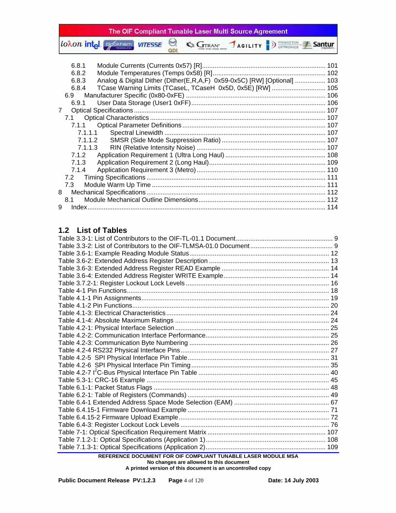
Figure 4.2-1 RS232 Timing shows the interface timing. The IRDY* indicates that a command is in process and that a packet will be returned. Once the packet is returned, the IRDY* line is asserted. The MS* line is not required to use the RS232 interface. It can be used to reset the serial interface and clear the I/O buffers on a low to high transition. By default, de-selecting the
19 This physical interface may be better described as an ASYNC interface but is usually referred to by the industry as an RS232 implementation. 20 Least significant bit 21 It is assumed that neither hardware or software flow control is needed to transfer a packet at the maximum data rate.
Start
Stop 0
1
2
3
4
5
6
7
REFERENCE DOCUMENT FOR OIF COMPLIANT TUNABLE LASER MODULE MSA No changes are allowed to this document
A printed version of this document is an uncontrolled copy
Public Document Release PV:1.2.3 Page 28 of 120 Date: 14 July 2003
module and then reselecting the module (MS*= low to high transition) will reset the interface baud rate to the default. This behavior can be modified by changing the IOCAP register.
Figure 4.2-1 RS232 Timing
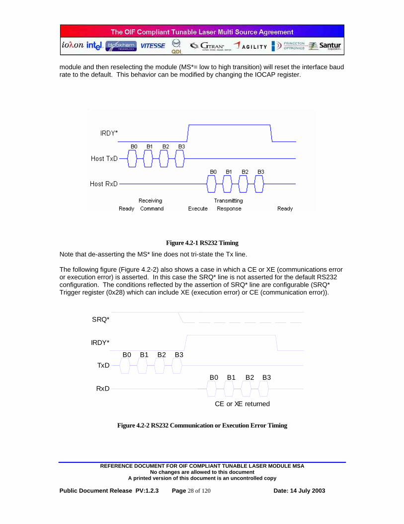
Note that de-asserting the MS* line does not tri-state the Tx line. The following figure (Figure 4.2-2) also shows a case in which a CE or XE (communications error or execution error) is asserted. In this case the SRQ* line is not asserted for the default RS232 configuration. The conditions reflected by the assertion of SRQ* line are configurable (SRQ* Trigger register (0x28) which can include XE (execution error) or CE (communication error)).
CE or XE returned
B0 B1 B2 B3
B0 B1 B2 B3
RxD
TxD
IRDY*
SRQ*
Figure 4.2-2 RS232 Communication or Execution Error Timing

REFERENCE DOCUMENT FOR OIF COMPLIANT TUNABLE LASER MODULE MSA No changes are allowed to this document
A printed version of this document is an uncontrolled copy
Public Document Release PV:1.2.3 Page 29 of 120 Date: 14 July 2003
If the command given was a tuning command, the ALM* line would be temporarily asserted. See Figure 4.2-3. The alarm line is asserted only while the alarming condition exists. The conditions reflected by the assertion of the ALM* line are configurable. A typical use for the ALM* signal would be to assert when the module’s output is not “locked” to a channel (ALM* = LOCK). This behavior is shown in Figure 4.2-3. The conditions for which this occurs are fully programmable.
B0 B1 B2 B3
B0 B1 B2 B3
Tuning
RxD
TxD
IRDY*
SRQ*
ALM*
Figure 4.2-3 Alarm Timing
The IOCap register has the following format when the RS232 interface is selected and assumes default values upon power up or hardware reset.
15 14 13 12 11 10 9 8 7 6 5 4 3 2 1 0 0x0 RMS 0x0 ASCII Current Baud Rate Supported Baud Rates
Bits 0-3 – Maximum baud rate supported by the module22. (Not writable)
0x00 – 9600 0x01 – 19200 0x02 – 38400 0x03 – 57600 0x04 – 115200 0x05 – 0x0F – Undefined
Bits 4-7 – The module’s currently configured baud rate (writable) (default 0x00) 0x00 – 9600 0x01 – 19200 0x02 – 38400 0x03 – 57600 0x04 – 115200 0x05 – 0x0F – Undefined
Bit 8 – ASCII - Enter ASCII interface debug mode when bit 8 is a 1, and exit when bit 8 is a 0. Bits 9-11 Reserved Bits 12 – RMS - Configurable action upon low to high transition of MS*
0x0 – Baud rate will be reset to default (0x00) and input buffer cleared upon low to high transition of MS* (default). This bit is for RS-232 mode only it has no affect in SPI mode 0x1 – Clear the input buffers but do not reset the baud rate.
22 The assumption is that the module will support all RS232 baud rates shown in the table to the specified maximum baud rate.

REFERENCE DOCUMENT FOR OIF COMPLIANT TUNABLE LASER MODULE MSA No changes are allowed to this document
A printed version of this document is an uncontrolled copy
Public Document Release PV:1.2.3 Page 30 of 120 Date: 14 July 2003
Bits 14-15 – Reserved (default 0x00) Note: Bit 8 of the RS232 Implementation’s IOCap register, when set to one, sets the interface to operate in ASCII mode. This feature is optional, and if not implemented, generates an XE (execution error). The response from the write IOCap is sent formatted as the interface was set to before bit 8 was set. Then the interface switches into the desired binary or ASCII mode. Commands must then be given in the following ASCII readable format:
[R,W] <REG_NO> <DATA><CR23>. (Example string: “W 0x03 0x0000\r”) Responses will be likewise readable: CE=[0,1] Status=[0-3] <REG_NO> <DATA><CRLF24>
(Example String: “CE=0 Status=0 0x03 0x0000\r\n”) To enter this mode, the command “W IOCap 0x0100\r” (0x010d 0x0100) is given. From a terminal keyboard, this is essentially the equivalent of pressing the <CR> key 4 times (0x0d0d, 0x0d0d). The interface can be reset to binary mode with the appropriate write iocap command or by sending any non-printable25 ASCII character (other than <CR>. The binary character is not lost and becomes the first byte of the binary command. This allows the interface to be easily reset should the interface accidentally be placed into ASCII mode. No checksum is done with the ASCII interface enabled. Therefore a transmission error can put the interface into binary mode. Of course, this is easily recoverable by sending 4 <cr> characters again. The 4 character ‘\r” (0x0d) sequence encodes the following: W 0x0D 0x0D0D (out-bound bytes 0-3)
7 6 5 4 3 2 1 0 BIP-4 = 0x0 Reserved = 0x6 1
7 6 5 4 3 2 1 0 Register = 0x0D
15 14 13 12 11 10 9 8 Reserved 0x0 BCMS=0 BRMS=0 Reserved 0x6 ASCII=1
7 6 5 4 3 2 1 0 Current Baud Rate=0x00 Supported Baud Rates (write
ignored)=0xD
23 CR – ASCII character 0x0D 24 CFLF – ASCII character sequence “0x0D + 0x0A” 25 Non-printable ASCII characters are 0x00-0x1F and 0x7F.

REFERENCE DOCUMENT FOR OIF COMPLIANT TUNABLE LASER MODULE MSA No changes are allowed to this document
A printed version of this document is an uncontrolled copy
Public Document Release PV:1.2.3 Page 31 of 120 Date: 14 July 2003
4.2.2 SPI Communications Interface
The SPI implementation used a standard 4-wire SPI interface with an additional line for communication packet pacing and an additional line for requesting attention. Both lines either can be used to generate interrupts or can be polled. The Serial Peripheral Interface (SPI) is essentially a shift register that serially transmits data bits to other SPI ports. During a data transfer, one SPI system acts as the “master” which controls the data flow, while the other system acts as the “slave” which has data shifted into and out of it by the master. The master device initiates all data transactions and every transaction is both a receive and a transmit operation. The master device transmits a new bit of data on the RxD pin and the slave device drives a new data bit on TxD pin on each active clock edge. However, only one slave may drive its output to write data back to the master at any given time. The master can be either a 8 bit, 16 bit, or 32 bit master and the slave is 32 bits. When the master is addressing the device, the module select signal (MS*) is driven low. The SPI slave device will immediately begin sending the transmit shift register contents to the TxD pin. The slave device also simultaneously reads the receiver shift register by shifting data in from the RxD pin. Thus a read and write transaction can be carried out simultaneously.
Figure 4.2-4 SPI IOCLK Timing
The SPI system consists of two data lines, a clock line, one control line, and a module select line.
Table 4.2-5 SPI Physical Interface Pin Table PIN SPI Name I/O FUNCTION
RxD MOSI input
LVTTL serial input Master Out Slave In - Abbreviated MOSI, this data line supplies the output data from the master which is shifted into the input(s) of the slave(s).
TxD MISO output
LVTTL serial output Master In Slave Out - Abbreviated MISO, this data line supplies the output data from a slave to the input of the master. There may be no more than one slave which is transmitting data during any particular transfer.
IOCLK
TxD, RxD
Data Latched In
RxD
TxD 32 bit Slave (Module) SPI Shift Register
8 bit Master (Host) SPI Shift Register
LSB MSB
LSB MSB

REFERENCE DOCUMENT FOR OIF COMPLIANT TUNABLE LASER MODULE MSA No changes are allowed to this document
A printed version of this document is an uncontrolled copy
Public Document Release PV:1.2.3 Page 32 of 120 Date: 14 July 2003
PIN SPI Name I/O FUNCTION
MS* SS* input
LVTTL serial input active low Module Select* - Abbreviated MS* (SS*), this control line allows slave’s TxD to be turned driven or tri-stated. Can be used to reset the communication’s interface.
IRDY* N/A output LVTTL (interface available/busy)
IOCLK SCLK Input
LVTTL serial input normally low I/O Clock - Abbreviated IOCLK (SCLK), this control line is driven by the master and regulates the flow of the data bits. The master may transmit data at a variety of baud rates; the SCLK line cycles once for each bit that is transmitted. This line is normally low. Inbound data is clocked on the rising edge and outbound data is clocked on the falling edge. The minimum clock speed26 is 1 MHz. All SPI devices will respond correctly at the minimum data rate. Faster data rates can be negotiated by reading the IOCAP register.
IOMODE N/A Input
IOMODE1 N/A Input
LVTTL serial input IOMODE and IOMODE1 determine the physical interface to be used..
IOMODE IOMODE1 Mode 0 0 SPI 1 0 RS232 0 1 I2C
1 1 Vendor Specific
These pins are read only on hard reset or power up. GND GND Ground Ground
The tunable device always acts as a slave device in this implementation. The communication occurs in packets of 4 byte transfers. The MS* line is held low during the entire 4 byte transfer. Raising the line anytime during the transfer aborts the packet transmission. Upon MS* returning high, the tunable device will begin any operations that were specified in the packet. The MS* line can be raised between an in-bound read command and the corresponding out-bound response. The following figure shows the timing for 1 byte capable host. A 4 byte capable host would have the same “Load-Read” timing as the slave.
26 A host may use any clock rate up to the maximum supported by the module. When a host first makes contact with a module, it can begin communications at a 1MHz clock rate or below to determine the maximum clock rate supported by the module. Further communication can be any clock rate up to the module’s maximum supported clock rate.

REFERENCE DOCUMENT FOR OIF COMPLIANT TUNABLE LASER MODULE MSA No changes are allowed to this document
A printed version of this document is an uncontrolled copy
Public Document Release PV:1.2.3 Page 33 of 120 Date: 14 July 2003
Figure 4.2-5 SPI Read (or Write) Timing, 1 Byte Host The command is complete when the IRDY* line is low. If the command was a READ command, the response can be read. If the packet was a WRITE command, a NOP can be sent to read the status bits CE and XE. In the event of an error (either communication error (CE) or execution error (XE)), the SRQ* (service request) line is asserted, if configured. See Figure 4.2-6.
1
2
3
4
5
6
7
8
9
10
11
12
13
14
15
16
17
18
19
20
21
22
23
24
25
26
27
28
29
30
31
32
1
2
3
4
5
6
7
8
9
10
11
12
13
14
15
16
17
18
19
20
21
22
23
24
25
26
27
28
29
30
31
32
IOCLK
TxD & RxD
SRQ*
Figure 4.2-6 SPI Error Timing (Execution or Communication)
Slave
Read Load
Master Load
IOCLK
MS*
IRDY*
Read Load
Read Load
Read Read Load
Load Read Load
Read Load
Read
Master loads “Read Serial No” Slave loads “NOP”
Load Read Load Read
Master loads “NOP” Slave loads “the Serial No”
Processing

REFERENCE DOCUMENT FOR OIF COMPLIANT TUNABLE LASER MODULE MSA No changes are allowed to this document
A printed version of this document is an uncontrolled copy
Public Document Release PV:1.2.3 Page 34 of 120 Date: 14 July 2003
The SRQ* line stays low until the appropriate status register bits are reset by a command (the default behavior). If the condition persists after the reset, the SRQ* line will again be asserted. The ALM* line is a non-latching version of SRQ and can be used to indicate loss of LOCK or any other programmable condition. When configured as a LOCK pin, it will be asserted during tuning. The IOCap register has the following format when the SPI interface is selected and assumes default values upon power up or hardware reset.
15 14 13 12 11 10 9 8 7 6 5 4 3 2 1 0 0x000 SPI Data Rate
Bits 0-5 – Maximum SPI data rate specified in MHz as an unsigned integer value. For example, the data rate maximum would be 20 MHz if Bits 5-0 are 0x14. Bits 6-15 – Reserved (default: 0x00)

REFERENCE DOCUMENT FOR OIF COMPLIANT TUNABLE LASER MODULE MSA No changes are allowed to this document
A printed version of this document is an uncontrolled copy
Public Document Release PV:1.2.3 Page 35 of 120 Date: 14 July 2003
Figure 4.2-7 SPI Transfer Timing
Table 4.2-6 SPI Physical Interface Pin Timing
Parameter Symbol Min Max Units Transfer Ready tRDY 30 - ns IOCLK Period tIOCLK 50 - ns IOCLK high or low time tWCLK 25 - ns SELECT to first clock tLEAD 25 - ns Last clock to SELECT tLAG 25 - ns DATA IN set up time tSU 10 - ns DATA IN hold time tH 10 - ns Slave access time tA - 15 ns TxD data valid tV - 15 ns Slave disable time tHO - 15 ns
IRDY
SELEC
IOCLK
RXD
TXD
tA
tRDY
tLEAD tIOCLK tWCLK tLAG
tSU
tV
t
Hi -Z Hi -ZOutput BIT-31
Input BIT-31
Input BIT-30
Input BIT-1
Input BIT-0
Output BIT-30
Output Output
tWCLK

REFERENCE DOCUMENT FOR OIF COMPLIANT TUNABLE LASER MODULE MSA No changes are allowed to this document
A printed version of this document is an uncontrolled copy
Public Document Release PV:1.2.3 Page 36 of 120 Date: 14 July 2003
4.2.3 I2C Communications Interface
Acknowledgement: Some text and figures for this section have been obtained from the Philips I2C-Bus specification. I2C-Bus is a simple bi-directional bus requiring only 2 bus lines – a serial data line (SDA) and a serial clock line (SCL) to communicate with multiple components attached to the bus. The I2C-Bus mechanical interface uses 5 connector pins – the clock, data line, and 3 address pins. The data link physical layer shall comply with the Philips specifications as defined in the I2C-Bus Specification, Version 2.1, January 2000. The 2 signals, Serial Data and Serial Clock, carry information between devices connected to the bus. Each device is recognized by a unique address and can operate as either a transmitter or receiver, depending on the function of the device. In addition to transmitters and receivers, devices can also be considered as masters or slaves when performing data transfers. A master is the device which initiates a data transfer on the bus, and generates the clock signals to permit that transfer, and terminates a transfer. At that time any other device connected to the bus is considered the slave, being addressed by the master. The I2C-Bus is a multi-master bus. More than one device capable of controlling the bus can be connected to it. The tunable module is connected as a slave only. The host is always the bus master. Both SDA and SCL are bi-directional lines, connected to a positive supply voltage via a current-source or pull-up resistor (see Figure 4.2-8). When the bus is free, both lines are HIGH. The output stages of devices connected to the bus must have an open-drain or open-collector to perform the wired-AND function. Data on the I2C-bus can be transferred at rates of up to 100 kbit/s in the Standard-mode, up to 400 kbit/s in the Fast-mode, or up to 3.4 Mbit/s in the High-speed mode. The IOCAP register can be used to declare the maximum supported data rate. Note that the I2C specification calls for the fast and high-speed data rates to be compatible with the slow or standard mode. The number of interfaces connected to the bus is solely dependent on the bus capacitance limit of 400 pF.

REFERENCE DOCUMENT FOR OIF COMPLIANT TUNABLE LASER MODULE MSA No changes are allowed to this document
A printed version of this document is an uncontrolled copy
Public Document Release PV:1.2.3 Page 37 of 120 Date: 14 July 2003
Figure 4.2-8 Connection of Standard and Fast mode devices to the I2C-Bus.
The data on the SDA line must be stable during the HIGH period of the clock. The HIGH or LOW state of the data line can only change when the clock signal on the SCL line is LOW (see Figure 4.2-9).
Figure 4.2-9 Bit transfer on the I2C-Bus
Within the procedure of the I2C-Bus, unique situations arise which are defined as START (S) and STOP (P) conditions (see Figure 4.2-10). A HIGH to LOW transition on the SDA line while SCL is HIGH is one such unique case. This situation indicates a START condition. A LOW to HIGH transition on the SDA line while SCL is HIGH defines a STOP condition. START and STOP conditions are always generated by the master. The bus is considered to be busy after the START condition. The bus is considered to be free again a certain time after the STOP condition. The bus stays busy if a repeated START (Sr) is generated instead of a STOP condition. In this respect, the START (S) and repeated START (Sr) conditions are functionally identical. Detection of START and STOP conditions by devices connected to the bus is easy if they incorporate the necessary interfacing hardware. However, microcontrollers with no such interface have to sample the SDA line at least twice per clock period to sense the transition.
Figure 4.2-10 Start and Stop conditions
Every byte put on the SDA line must be 8-bits long. The number of bytes that can be transmitted per transfer is unrestricted. However, for the tunable module source – packets are restricted to 4 bytes and are governed by layers B and C. Each byte has to be followed by an acknowledge bit. Data is transferred with the most significant bit (MSB) first (see Figure 4.2-11). If a slave can’t receive or transmit another complete byte of data until it has performed some other function, for example servicing an internal interrupt, it can hold the clock line SCL LOW to force the master

REFERENCE DOCUMENT FOR OIF COMPLIANT TUNABLE LASER MODULE MSA No changes are allowed to this document
A printed version of this document is an uncontrolled copy
Public Document Release PV:1.2.3 Page 38 of 120 Date: 14 July 2003
into a wait state. Data transfer then continues when the slave is ready for another byte of data and releases clock line SCL. As a slave is capable of seizing the bus, a maximum wait state is imposed. A byte wait state shall not exceed the time of 1 minimum rate byte (9 bits including the acknowledge or 100 microseconds with a minimum rate of 90 kHz). The host shall not pause more than 1 minimum rate byte (9 bits including the acknowledge) between bytes of an ongoing message. The use of wait states is discouraged. A tunable module cannot use the clock line to indicate that a command in processing, before issuing a response. The module generates the IRDY* line to indicate that a command is executing. The host can either monitor the IRDY* line or poll the module to determine when the command is complete.
Figure 4.2-11 Data Transfer on the I2C-Bus
Data transfer with acknowledge is obligatory. The acknowledge-related clock pulse is generated by the master. The transmitter releases the SDA line (HIGH) during the acknowledge clock pulse. The receiver must pull down the SDA line during the acknowledge clock pulse so that it remains stable LOW during the HIGH period of this clock pulse (see Figure 4.2-12). Of course, set-up and hold times must also be taken into account. Usually, a receiver which has been addressed is obliged to generate an acknowledge after each byte has been received. When a slave doesn’t acknowledge the slave address (for example, it’s unable to receive or transmit because it’s performing some real-time function), the data line must be left HIGH by the slave. The master can then generate either a STOP condition to abort the transfer, or a repeated START condition to start a new transfer. If a slave-receiver does acknowledge the slave address but, some time later in the transfer cannot receive any more data bytes, the master must again abort the transfer. This is indicated by the slave generating the not-acknowledge on the first byte to follow. The slave leaves the data line HIGH and the master generates a STOP or a repeated START condition. If a master-receiver is involved in a transfer, it must signal the end of data to the slave- transmitter by not generating an acknowledge on the last byte that was clocked out of the slave. The slave-transmitter must release the data line to allow the master to generate a STOP or repeated START condition.
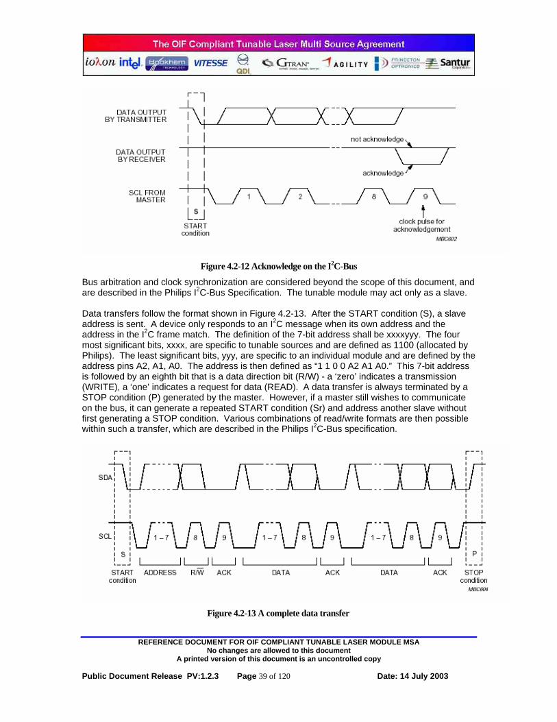
REFERENCE DOCUMENT FOR OIF COMPLIANT TUNABLE LASER MODULE MSA No changes are allowed to this document
A printed version of this document is an uncontrolled copy
Public Document Release PV:1.2.3 Page 39 of 120 Date: 14 July 2003
Figure 4.2-12 Acknowledge on the I2C-Bus
Bus arbitration and clock synchronization are considered beyond the scope of this document, and are described in the Philips I2C-Bus Specification. The tunable module may act only as a slave. Data transfers follow the format shown in Figure 4.2-13. After the START condition (S), a slave address is sent. A device only responds to an I2C message when its own address and the address in the I2C frame match. The definition of the 7-bit address shall be xxxxyyy. The four most significant bits, xxxx, are specific to tunable sources and are defined as 1100 (allocated by Philips). The least significant bits, yyy, are specific to an individual module and are defined by the address pins A2, A1, A0. The address is then defined as “1 1 0 0 A2 A1 A0.” This 7-bit address is followed by an eighth bit that is a data direction bit (R/W) - a ‘zero’ indicates a transmission (WRITE), a ‘one’ indicates a request for data (READ). A data transfer is always terminated by a STOP condition (P) generated by the master. However, if a master still wishes to communicate on the bus, it can generate a repeated START condition (Sr) and address another slave without first generating a STOP condition. Various combinations of read/write formats are then possible within such a transfer, which are described in the Philips I2C-Bus specification.
Figure 4.2-13 A complete data transfer.

REFERENCE DOCUMENT FOR OIF COMPLIANT TUNABLE LASER MODULE MSA No changes are allowed to this document
A printed version of this document is an uncontrolled copy
Public Document Release PV:1.2.3 Page 40 of 120 Date: 14 July 2003
The I2C-Bus system requires 1 data line, 1 clock line. Each Tunable Laser module requires 3 address pins, which are hard wired to a fixed address code. I2C-Bus pins are defined in Table 4.2-7 below.
Table 4.2-7 I2C-Bus Physical Interface Pin Table PIN NO. PIN I2C Name I/O FUNCTION
16 RxD SDA Input/output LVTTL serial input/output Serial Data line
20 IOCLK SCL Input/output LVTTL serial input/output Serial Clock line
26 N/A A0 Input 28 N/A A1 Input
30 N/A A2 Input
LVTTL input Address lines are only read on power up or hardware reset to set device address (A2, A1, A0); A0 is the LSB.
22 IOMODE N/A
24 IOMODE1 N/A
Input
IOMODE and IOMODE1 determine the physical interface to be used.
IOMODE IOMODE1 Mode 0 0 SPI 1 0 RS232 0 1 I2C
1 1 Vendor Specific
These pins are read only on hard reset or power up.
4 MS* N/A Input
LVTTL input Not required. Can be used to reset communications and clear transport layer communication buffers on a low to high transition
18 IRDY* N/A Output
LVTTL output, active low Controlled by the transport layer. Indicates when the unit is still executing a previous command and not ready for the response to be read.
An I2C-Bus interface does not require use the IRDY* (interface available/busy) pin although it is supported27. The MS* (module select) pin is used only to clear in the input buffer and reset the communications interface28. The bus is considered busy after generating a Start command, and is free after a Stop command. The packet length is a fixed size and is framed by the Start and Stop symbols. A module is selected using the I2C-Bus slave address bits, and does not require a separate select line.
27 The IRDY* line can be used by the host to determine that the module is currently executing a command and not available for communication. This can be useful if the host is restarted while the module is executing a (long) command. If the IRDY* line not used, a polling scheme is required. It can also be used to advise the host when to continue clocking to read the response. 28 The behavior is preserved to keep the transport and application layers identical although it is not required for normal I2C operation.

REFERENCE DOCUMENT FOR OIF COMPLIANT TUNABLE LASER MODULE MSA No changes are allowed to this document
A printed version of this document is an uncontrolled copy
Public Document Release PV:1.2.3 Page 41 of 120 Date: 14 July 2003
The use of the Start and Stop commands is demonstrated in Figure 4.2-13 above, which shows how the 4-byte packets are received by the module and transmitted from the module. The first transfer of the 4 bytes is an I2C “W” command independent of whether the application layer command is a read or a write. When the module is finished processing, the host issues an I2C “R” command to read the response. The application layer defines a maximum timeout for commands. If the module will exceed this time during the execution, the module will return a response which includes indication of a pending operation. In either case, the host must either check the IRDY* line or poll the module through the I2C interface to determine if the module is ready with a response. The use of the IRDY* by the host is purely optional but is provided for compatibility with the transport layer29 as well as allowing for faster transfer rates by eliminating the bus transfers during polling30.
The IOCap register is defined as follows for the I2C bus.
29 Note that the IRDY* line may be necessary under certain conditions depending upon the particular I2C implementation 30 This also increases the availability of the I2C bus for use with other devices.
Start – from Host
Module address byte
4 received Bytes from host
0
Stop –from Host Start –
from Host
4 transmitted Bytes to host from module
Module address byte
Stop –from Host
Execute
1 2 3 0 1 2 3 SDA
Figure 4.2-14 Receipt and Transmit of 4 Byte packets

REFERENCE DOCUMENT FOR OIF COMPLIANT TUNABLE LASER MODULE MSA No changes are allowed to this document
A printed version of this document is an uncontrolled copy
Public Document Release PV:1.2.3 Page 42 of 120 Date: 14 July 2003
15 14 13 12 11 10 9 8 7 6 5 4 3 2 1 0
0x000 Max Supported I2C Data Rate
Bits 2-0 – Maximum supported I2C data rate specified in the table below. Default manufacturer specific.
I2C Data Rate Value (Bits 2,1,0) I2C Data Rate
0x0 Standard 100kbits/s 0x1 Fast 400 kbits/s 0x2 High Speed 3.4Mbits/s
0x3-0x7 Reserved Note that a given interface speed is compatible with all lower valued data rates. Bits 15-3 – Reserved (default: 0x00)

REFERENCE DOCUMENT FOR OIF COMPLIANT TUNABLE LASER MODULE MSA No changes are allowed to this document
A printed version of this document is an uncontrolled copy
Public Document Release PV:1.2.3 Page 43 of 120 Date: 14 July 2003
5 Transport Layer
5.1 Overview The transport layer encapsulates the command and response packets to form a 32-bit frame. Figure 5.1-1 and Figure 5.1-2 depict the in-bound and out-bound frames. The transport layer is responsible for the fields in white. The application layer is responsible for the shaded fields below. Note that the high order bit (left most bit) is numbered 31.
Figure 5.1-1: In-Bound (Host to Module) Frame 31 30 29 28 Bits 27:0
Checksum Command packet being framed
Figure 5.1-2 Out-Bound (Module to Host) Frame 31 30 29 28 27 26 Bits 25:0
Checksum CE Response Response packet being framed
Figure 5.1-3 Transport Layer Field Definitions
Field In-Bound (Host to Module)
Out-Bound (Module to Host)
Application Layer Packet to be Framed
28 bits Bits 27:0
26 bits Bits 25:0
Checksum Bits 31:28
BIP-4 checksum computed over a 32 bit word with the leading 4 bits pre-pended to the 28 bit packet and set to zero.
BIP-4 checksum computed over a 32 bit word with the bits 31:28 set to zero and bits 27:26 defined by the transport layer prior to the BIP-4 computation.
CE Bit 27 (Communication Error)
N/A
Bit set to logic 0 when the checksum (and/or optional CRC check) are consistent. Bit set to logic 1 when the checksum (and/or optional CRC check) are inconsistent.
Response Flag Bit 26 N/A
Bit set to logic 1 when the response packet contains a response to a request to read (data returned). Bit set to logic 0 when the response packet contains no useable data31.
Each in-bound and out-bound packet contains a 4 bit checksum. The checksum is computed over all the bits being encapsulated using a BIP-4 checksum. A CRC-16 is also available using registers 0x11-0x13
5.2 Checksum The checksum is a BIP-432 checksum is computed by xor’ing all the bytes in the packet together and then xor’ing the left nibble of the result with the right nibble of the result.
31 Some physical interfaces such as SPI return response to every command even if the command didn’t request any data to be returned.

REFERENCE DOCUMENT FOR OIF COMPLIANT TUNABLE LASER MODULE MSA No changes are allowed to this document
A printed version of this document is an uncontrolled copy
Public Document Release PV:1.2.3 Page 44 of 120 Date: 14 July 2003
The checksum provides a basic level of consistency check for the communications transfer.
unsigned char calcBIP4( unsigned char* data ) { int i; unsigned char bip8=(data[0]& 0x0f) ^ data[1] ^ data[2] ^ data[3]; unsigned char bip4=((bip8 & 0xf0) >>4) ^ (bip8 & 0x0f); return bip4; } #include <stdio.h> int main(int argc, char** argv) { int i, input_char; unsigned char data[4]; unsigned char bip4; if (argc!=5) { fprintf(stderr,"Usage: ChkSum hexdata0 hexdata1 hexdata2 hexdata3\n"); fprintf(stderr," Example:Usage: ChkSum 0x0d 0x0d 0x0d 0x0d\n"); exit(1); } for (i=1; i<5; i++) { sscanf(argv[i],"%x",&input_char); data[i-1]=(unsigned char) input_char; } bip4=calcBIP4(data); printf("Packet prior to checksum %2.2x %2.2x %2.2x %2.2x\n", data[0], data[1],data[2],data[3]); data[0]|= (bip4<<4); /* Add in the BIP-4 checksum */ printf("Bip-4 checksum value is %x\n",bip4); printf("Packet with checksum %2.2x %2.2x %2.2x %2.2x\n", data[0], data[1],data[2],data[3]); }
5.3 CRC-16
For increased robustness of the communication interface, the module can be configured to support a full 16-bit CRC33. This option is only recommended for implementations where the integrity of the communication’s interface is paramount. The CRC-16 mode is enabled through the General Module Configuration register (0x08). The CRC can be computed by the following C program. #define CRC16 0xA001 /* X16 + X15 + X2 + 1 */ unsigned short calcCRC( unsigned short crc, unsigned short data ) { int i; for ( i = 8; i; i-- ) { if (( data ^ crc ) & 0x0001) crc = ( crc >> 1 ) ^ CRC16; else crc >>= 1; data >>= 1; } return crc; } #include <stdio.h> int main(int argc, char** argv) { unsigned short crc = 0; int i; int data; if (argc!=5) {
32 Bits interleaved parity four bits wide 33 The CRC-16 is computed over the entire 32 bit packet including the BIP-4 checksum field.

REFERENCE DOCUMENT FOR OIF COMPLIANT TUNABLE LASER MODULE MSA No changes are allowed to this document
A printed version of this document is an uncontrolled copy
Public Document Release PV:1.2.3 Page 45 of 120 Date: 14 July 2003
fprintf(stderr,"Usage: crc16 hexdata0 hexdata1 hexdata2 hexdata3\n"); fprintf(stderr," Example:Usage: crc16 0x0d 0x0d 0x0d 0x0d\n"); fprintf(stderr," CRC-16 is 3a56\n"); exit(1); } crc=0; for (i=1; i<5; i++) { sscanf(argv[i],"%x",&data); crc=calcCRC(crc,(short) data); } printf("CRC-16 is %x\n",crc); }
An example utilizing the CRC-16 capability is shown in Table 5.3-1.
Table 5.3-1: CRC-16 Example Command (Host to Module) Response (Module to Host)
# Operation Register Data
Bytes (15:0)
Packet Status Register Data
Bytes (15:0)
Packet
1 Write 0x11 (WCRC) 0x0A0A 0x1111, 0x0A0A 0x00 0x11 (WCRC) 0x0000 0x4411,
0x0000
2 Read 0x02 (Status Fatal) 0x0000 0x2020, 0x0000 0x00 0x20 (Status,fatal) 0x0000 0x6420,
0x0000
3 Read 0x12 (RCRC) 0x0000 0x3012, 0x0000 0x00 0x12 (RCRC) 0xFA1E 0x0412,
0xFA1E In step 1, the CRC-16 is computed for the full 32-bit command packet in step 2 and asserted by writing to the WCRC register. After the status register is read in step 2, the RCRC register is read to retrieve the CRC-16 value the module computed for its response packet in step 2. For the in-bound command, the module will generate a CE (Communications Error) if the CRC-16 doesn’t match the assertion in step 1. For the out-bound command, the host must compare the returned CRC-16 in step 3 with its own CRC-16 calculation on the response in step 2.
5.4 Packet Pacing The physical interfaces use the IRDY* line (Interface Ready) to signal that the interface is available to receive the next packet. Figure 5.4-1 shows the IRDY* timing. This signal is required by the SPI interface but can improve the robustness of the other interfaces.
IRDY*
SRQ*
In-bound packet
Out-bound packet
Command Execution

REFERENCE DOCUMENT FOR OIF COMPLIANT TUNABLE LASER MODULE MSA No changes are allowed to this document
A printed version of this document is an uncontrolled copy
Public Document Release PV:1.2.3 Page 46 of 120 Date: 14 July 2003
Figure 5.4-1 Packet Pacing Example
The host watches the IRDY* line. When it is low, the host can begin transmission of a command to the module. The IRDY* line goes high after the last byte of the packet is received. At the end of the packet, the module can decode it and begin execution. The IRDY* line will remain high and return low after the execution completes or terminates in error. The module is never allowed to transmit an out-bound packet without a request from the host.

REFERENCE DOCUMENT FOR OIF COMPLIANT TUNABLE LASER MODULE MSA No changes are allowed to this document
A printed version of this document is an uncontrolled copy
Public Document Release PV:1.2.3 Page 47 of 120 Date: 14 July 2003
6 Command Interface (Application Layer)
6.1 Command Format
6.1.1 In-Bound (Host to Module) The command packets consist of a 4 byte packet of which the lower 28 bits are used. The 4 high order bits are redefined by the transport layer (where the packet checksum is added). The shaded area shows the bits to be replaced by the transport layer.
Inbound Byte 0 31 30 29 28 27 26 25 24
0x0 (To be defined by transport layer) 0x0 RW
Inbound Byte 1 23 22 21 20 19 18 17 16
Register Number (0x00 – 0xff)
Inbound Byte 2 15 14 13 12 11 10 9 8
Data 15:8
Inbound Byte 3 7 6 5 4 3 2 1 0
Data 7:0
6.1.2 Out-Bound (Module to Host) The response packet consists of a 4 byte packet of which the lower 26 bits are used. The 6 high order bits contain a checksum and two flags which are redefined by the transport layer. The shaded area shows the bits to be replaced by the transport layer.
Outbound Byte 0
31 30 29 28 27 26 25 24 0x0 (To be defined by transport layer) Status
Outbound Byte 1
23 22 21 20 19 18 17 16 Register Number (0x00 – 0xff)
Outbound Byte 2
15 14 13 12 11 10 9 8 Data 15:8
Outbound Byte 3
7 6 5 4 3 2 1 0 Data 7:0
The status field (bits 25:24) take on one of the 4 values in Table 6.1-1.

REFERENCE DOCUMENT FOR OIF COMPLIANT TUNABLE LASER MODULE MSA No changes are allowed to this document
A printed version of this document is an uncontrolled copy
Public Document Release PV:1.2.3 Page 48 of 120 Date: 14 July 2003
Table 6.1-1: Packet Status Flags Bits 1:0 Value Status Field
0x00 OK flag, Normal return status 0x01 XE flag, (execution error) 0x02 AEA flag, (Automatic extended addressing result being returned or ready to
write) 0x03 CP flag, Command not complete, pending
Bits 1:0=0x00, OK flag, Normal. No execution errors and not using AEA mode for returning result. Bits 1:0=0x01, XE flag (Execution Error) signifies that the previous command failed to execute properly. (Bits 1:0) not equal 0x01 signifies that the previous command completed successfully or is pending.
Bits 1:0=0x02, AEA flag, (automatic extended addressing) mode, indicates that the register (for which a read or write operation has been given) requires a multi-byte sequence34. The unsigned value is returned in bytes 2 and 3 and represents the number of bytes in the multi-byte response. Bits 1:0=0x03, CP flag, Command pending (command not complete), indicates that the command will take longer than the maximum timeout specified for this device type.35 In this case the module returns a response within the timeout period and continues to execute the requested operation. The host can poll the module’s status register (0x00) through the communication’s interface to determine if the operation has completed.
If the CP flag is set, the out-bound byte 3 will be 0x00 and out-bound byte 2 will have one of eight bits set (bits 15:8) showing which bit the pending operation has been assigned. Note that this bit mapping is identical to the bits 15:8 in the response of the NOP (x000) command.
34 In the case where a write was done to a register that supports AEA, outbound bytes 2 and 3 are ignored. The write command will need to be repeated this time addressing the AEA-EAR register instead. 35 Device types/classes are specific implementations of tunable devices. See §10.1 for a table of device type assignments

REFERENCE DOCUMENT FOR OIF COMPLIANT TUNABLE LASER MODULE MSA No changes are allowed to this document
A printed version of this document is an uncontrolled copy
Public Document Release PV:1.2.3 Page 49 of 120 Date: 14 July 2003
6.2 Register Summary
Table 6.2-1: Table of Registers (Commands) Command Register
Name Read / Write AEA NV /
Lock? Description
General Module Commands
0x00 NOP R/W
Provide a way to read a pending response as from an interrupt, to determine if there is pending operation, and/or determine the specific error condition for a failed command.
0x01 DevTyp R AEA Returns device type (tunable laser source, filter, modulator, etc) as a null terminated string.
0x02 MFGR R AEA Returns manufacturer as a null terminated string in AEA mode (vendor specific format)
0x03 Model R AEA Returns a model null terminated string in AEA mode (vendor specific format)
0x04 SerNo R AEA Returns the serial number as null terminated string in AEA mode
0x05 MFGDate R AEA Returns the mfg date as a null terminated string.
0x06 FW R AEA Returns a manufacturer specific firmware release as a null terminated string in AEA mode
0x07 RelBack R AEA Returns manufacturer specific firmware backwards compatibility as a null terminated string
0x08 GenCfg RW NV Lockable 2 General module configuration
0x09 AEA-EAC R Automatic extended address configuration register
0x0A AEA-EA R Automatic extended address (16 bits) 0x0B AEA-EAR RW Lockable 1 Location accessed “thru” AEA-EA and AEA-EAC 0x0C Reserved
0x0D IOCap RW NV Lockable 2
Physical interface specific information in string form (such as data rate, etc.)
0x0E EAC RW Lockable 3 Extended address configuration register - auto incr/decr flag on read and on write and additional address bits
0x0F EA RW Lockable 3 Extended address (16 bits) 0x10 EAR RW Location accessed “thru” EA and EAC 0x11 WCRC W Asserts CRC16 for next command packet 0x12 RCRC R Returns CRC16 for last response packet 0x13 LstResp R Returns last response 0x14 DLConfig RW Lockable 2 Download configuration register 0x15 DLStatus R Download status register 0x16 Lock RW AEA Register Lockout Enable/Disable
0x17 – 0x1F Reserved -- --

REFERENCE DOCUMENT FOR OIF COMPLIANT TUNABLE LASER MODULE MSA No changes are allowed to this document
A printed version of this document is an uncontrolled copy
Public Document Release PV:1.2.3 Page 50 of 120 Date: 14 July 2003
Module Status Commands
0x20 StatusF RW Contains reset status, optical faults and alarms, and enable status.
0x21 StatusW RW Contains reset status, warning optical faults and alarms, and enable status.
0x22 FPowTh RW NV Lockable 2
Returns/Sets the threshold for the output power FATAL condition encoded as ±dB*100
0x23 WPowTh RW NV Lockable 2
Returns/Sets the threshold for the power warning encoded as ±dB*100
0x24 FFreqTh RW NV Lockable 2
Returns/Sets the threshold for the frequency FATAL condition encoded as ±GHz*10
0x25 WFreqTh RW NV Lockable 2
Returns/Sets the threshold for the frequency error warning encoded as ±GHZ*10
0x26 FThermTh RW NV Lockable 2
Returns/Sets the threshold for thermal deviations (> ±°C*100) at which FATAL is asserted.
0x27 WThermTh RW NV Lockable 2
Returns/Sets the threshold for thermal deviations (> ±°C*100) at which a warning is asserted.
0x28 SRQT RW NV Lockable 2
Indicates which bits in the Fatal & Warning status registers, 0x20-0x21, cause a SRQ condition and asserts the SRQ* line.
0x29 FatalT RW NV Lockable 2
Indicates which bits in the Fatal & Warning status register, 0x20-0x21, cause a FATAL condition and asserts the FATAL* line.
0x2A ALMT RW NV Lockable 2
Indicates which bits in the status registers, 0x20, 0x21, cause an alarm condition and asserts the alarm line (Default behavior asserted whether laser is LOCKED on frequency.
0x2B – 0x2F Reserved
Module Optical Commands 0x30 Channel RW NV
Lockable 1 Setting valid channel causes a tuning operation to occur.
0x31 PWR RW NV Lockable 1
Sets the optical power set point as encoded as dBm*100
0x32 ResEna RW Lockable 1 Reset/Enable - Enable output, hard and soft reset
0x33 MCB RW NV Lockable 2 Various module configurations
0x34 GRID RW NV Lockable 2
Allows the grid spacing to be set for channel numbering.
0x35 FCF1 RW NV Lockable 2
Allows the first channel’s frequency to be defined for channel numbering. (THz)
0x36 FCF2 RW NV Lockable 2
Allows the first channel’s frequency to be defined for channel numbering. (GHz*10)
0x37 – 0x3F Reserved Reserved for OIF configuration registers
0x40 LF1 R Returns channel’s frequency as THz 0x41 LF2 R Returns channel’s frequency as GHZ*10 0x42 OOP R Returns the optical power encoded as dBm*100
0x43 CTemp R AEA Returns the current temperature (monitored by the temperature alarm) encoded as °C*100.
0x44 – 0x4F Reserved Reserved for OIF status registers

REFERENCE DOCUMENT FOR OIF COMPLIANT TUNABLE LASER MODULE MSA No changes are allowed to this document
A printed version of this document is an uncontrolled copy
Public Document Release PV:1.2.3 Page 51 of 120 Date: 14 July 2003
Module Capabilities
0x50 OPSL R Returns the min possible optical power setting 0x51 OPSH R Returns the max possible optical power setting 0x52 LFL1 R Laser’s first frequency (THz) 0x53 LFL2 R Laser’s first frequency (GHz*10) 0x54 LFH1 R Laser’s last frequency (THz) 0x55 LFH2 R Laser’s last frequency (GHz*10)
0x56 LGrid R Laser’s minimum supported grid spacing (GHz*10)
MSA Commands 0x57 Currents R AE
A Return module specific currents
0x58 Temps R AEA Return module specific temperatures
0x59 DitherE RW NV Lockable 1 Digital dither enable
0x5A DitherR RW NV Lockable 2 Digital dither rate
0x5B DitherF RW NV Lockable 2
Digital dither frequency modulation
0x5C DitherA RW NV Lockable 2
Digital dither amplitude modulation
Optional features
0x5D TCaseL RW NV Lockable 2
Sets the lower boundary for a warning on case temperature
0x5E TCaseH RW NV Lockable 2
Sets the upper boundary for a warning on case temperature
0x5F- 0x7F Reserved Manufacturer Specific
0x80-0xFE Manufacturer Specific
0xFF User1 RW AEA NV Lockable 1 User area 1 – Store / retrieve user data

REFERENCE DOCUMENT FOR OIF COMPLIANT TUNABLE LASER MODULE MSA No changes are allowed to this document
A printed version of this document is an uncontrolled copy
Public Document Release PV:1.2.3 Page 52 of 120 Date: 14 July 2003
6.3 Command Description Format
The commands are described using 5 sections (note the shaded boxes in the table represent fields that are not applicable):
1) Purpose – Describes the basic
purpose of the command. 2) Synopsis – Tabular format
summarizing the command behavior and arguments
3) Returns – Tabular format summarizing the possible returns for successful and error conditions. Status field (register 0x00) Error condition field (0x00) Data value (16 bit) Effect on module Execution time Pending operation
4) Detailed Description – Describes the detailed behavior of the command 5) Data Value Description – Describes the data value for the command. The Synopsis section describes the following:
Every command will show two lines; one for read and one for write. In the case of a read, the data value type is shown for the response packet. For a write, the data value type is shown as the operand of the command. (Note the shaded boxes in the table represent fields that are not applicable):
1) The “Response Generated” column indicates the maximum interval of time from when the command is acknowledged by the module until the module will generate a response. The transmission time of the response is dependent on the physical interface data rate and characteristics. See §4.2-Communication Interfaces.
2) The “Can Be Pending” column indicates if the command is allowed not to finish in the “Response Generated” time interval.
3) The “Volatile” column, if contains non-volatile, indicates that the default value loaded during power up or hard reset is loaded from non-volatile memory36. The defaults may be configured and stored using the GenCfg:SDC operation. See §6.4.9-General Module Configuration (GenCfg 0x08) [RW].
36 The default configuration is typically user application specific and once configured is expected to be infrequently modified. Most of these parameters are defined as lock level 2.

REFERENCE DOCUMENT FOR OIF COMPLIANT TUNABLE LASER MODULE MSA No changes are allowed to this document
A printed version of this document is an uncontrolled copy
Public Document Release PV:1.2.3 Page 53 of 120 Date: 14 July 2003
4) The “Access” column indicates if the register can be locked for write access through the module’s register lockout capability. Lockable registers have four lock levels. See §6.4.17-Register Lockout (Lock 0x16) [RW].
5) Where relevant, the “Default Contents” column indicates what the default contents would be for a freshly booted or reset module. Note that registers marked non-volatile have defaults values set by the GenCfg:SDC operation.
The Returns section describes the following for successful and failed read and write operations.
1) Status Field Returned: The value in the status field (bits 25:24) in the out-bound response (module to host).
2) Error Condition Field: The possible values contained in the NOP (0x00) commands error field because of the command’s execution or failure to execute.
3) Data Value: A description of the data value contained in the modules response. 4) Effect on Module: Indicates the resultant state of the module after requested
operation has terminated. 5) Execution Time:The maximum time for the command to complete execution. Note
this is different than the generation of a response described in the previous table. 6) Pending Operation: Indicates whether a successful command can return before the
command has completed execution.

REFERENCE DOCUMENT FOR OIF COMPLIANT TUNABLE LASER MODULE MSA No changes are allowed to this document
A printed version of this document is an uncontrolled copy
Public Document Release PV:1.2.3 Page 54 of 120 Date: 14 July 2003
6.4 Generic Module Commands
6.4.1 NOP/Status (NOP 0x00) [RW] Purpose
The NOP register provides a way to access the module’s status, returning pending operation status, and the current value of the error field. This register may be read upon receiving an execution error for an immediately preceding command. It can also be polled to determine the status of pending operations.
Synopsis: Register
Name Register Number
Read / Write
Data Type Read or Written
Response Generated
Can Be Pending?
Volatile? Access? Default Contents
R Unsigned short See §7.2 No
Bits15:8: 0x00 (pending bits) Bit 7:6: Locked (non-volatile) Bit 5: MRDY (0x0) Bit 4: 0x0 (reserved) Bits 3:0: 0x0 (error field)
NOP 0x00
W Unsigned short See §7.2 No Not locked
Returns Data Value Returned in Response Upon Successful Read Successful Write Error on Read Error on Write
Status Field Returned: OK OK XE XE Error Condition Field: OK OK CIP, CII, EXF, or VSE CIP, CII, EXF, or VSE
Data Value:
Pending command status (bits 15:8), Bit 7:6, 4, and error condition field (bits 3:0)
Same as was sent 0x0000 0x0000
Effect on Module None, by definition None, by definition Error field set Error field set Execution Time: See §7.2 See §7.2 See §7.2 See §7.2 Pending Operation: Never Never
Detailed Description
A write to the NOP register is allowed but the contents are not loaded with the data value from the write command.
Data Value Description
15 14 13 12 11 10 9 8 7 6 5 4 3 2 1 0 Pending Operation Status Locked 0x0 MRDY Error Field
Bits 15:8 – Pending Operation Flags
A series of eight flag bits indicating which operations, if any, are still pending. Each operation that becomes pending is assigned one of these four bit positions. The module can be periodically polled (by reading the NOP register) to determine which operations have completed. A value of 0x0 indicates that there are no currently pending operations.
Bit 7:6 - Locked When non-zero, indicates that the registers listed as “Lockable” are locked or read only as per the lock level. Note that the module’s default lock level is configurable with GenCfg:SDC.

REFERENCE DOCUMENT FOR OIF COMPLIANT TUNABLE LASER MODULE MSA No changes are allowed to this document
A printed version of this document is an uncontrolled copy
Public Document Release PV:1.2.3 Page 55 of 120 Date: 14 July 2003
When “0”, indicates that all the registers listed as “Lockable” are write-able. Bit 5– Always 0x00 (Reserved) Bit 4 – MRDY - Module Ready37
When “1” indicates that the module is ready for its output to be enabled When “0” indicates that the module is not ready for its output to be enabled.
Bits 3:0 – Error field – Error condition for last command A read of the NOP register will return the error condition from the last command before setting it to 0x00 to reflect the status of the current command (which is reading the NOP register).
Value
(Bits 3:0) Symbol Meaning
0x00 OK Ok, no errors 0x01 RNI The addressed register is not implemented 0x02 RNW Register not write-able; register cannot be written (may be locked or read
only) 0x03 RVE Register value range error; writing register contents causes value range
error; contents unchanged 0x04 CIP Command ignored due to pending operation 0x05 CII Command ignored while module is initializing, warming up, or contains an
invalid configuration. 0x06 ERE Extended address range error (address invalid) 0x07 ERO Extended address is read only 0x08 EXF Execution general failure 0x09 CIE Command ignored while module’s optical output is enabled (carrying
traffic) 0x0A IVC Invalid configuration, command ignored
0x0B-0x0E -- Reserved for future expansion 0x0F VSE Vendor specific error (see vendor specific documentation for more
information)
The device type register is provided such that a host can distinguish between different types of tunable devices.
6.4.2 Device Type (DevTyp 0x01) [R] Purpose:
DevTyp returns the module’s device type. For all tunable lasers covered by this MSA, the module will return the null terminated string “CW Laser\0” (nine bytes including the terminating null character) indirectly through the AEA mechanism. The device type register is provided such that a host can distinguish between different types of tunable devices.
Synopsis: Register
Name Register Number
Read / Write
Data Type Read or Written
Response Generated
Can Be Pending?
Volatile? Access? Default Contents
R AEA (string) See §7.2 No 0x0009 “CW Laser\0” DevTyp 0x01
W
37 De-asserted during module warm up time (see §7.3-Module Warm Up Time) or if an invalid configuration detected. Asserted when module is ready to enable output and carry traffic.

REFERENCE DOCUMENT FOR OIF COMPLIANT TUNABLE LASER MODULE MSA No changes are allowed to this document
A printed version of this document is an uncontrolled copy
Public Document Release PV:1.2.3 Page 56 of 120 Date: 14 July 2003
Returns Data Value Returned in Response Upon Successful Read Successful Write Error on Read Error on Write
Status Field Returned: OK XE Error Condition Field: OK CIP, CII, EXF, or VSE
Data Value: 0x0009 “CW Laser\0” 0x0000
Effect on Module AEA registers configured to reference string
Error field set
Execution Time: See §7.2 See §7.2 Pending Operation: Never
Detailed Description
A write to the DevTyp register results in an execution error.
Data Value Description DevTyp returns the length of ASCII string. Note that in this case, the null terminated string “CW Laser\0” contains nine bytes including the null terminating byte.
Example Usage
Command (Host to Module) Response (Module to Host) # Operation Register
Data Bytes (15:0)
Status Register Data Bytes (15:0)
Read 0x01 (DevTyp) 0x0000 0x02 (AEA-flag) 0x01 DevTyp 0x0009 (# bytes in string) 1
Note: When the Read is completed, registers (0x09, and 0x0A) are configured to point to proper field. 2 Read 0x0B (AEA-EAR) 0x0000 0x00 0x0B (AEA-EAR) 0x4357 (“CW”) 3 Read 0x0B (AEA-EAR) 0x0000 0x00 0x0B (AEA-EAR) 0x204C (“ L”) 4 Read 0x0B (AEA-EAR) 0x0000 0x00 0x0B (AEA-EAR) 0x6173 (“as”) 5 Read 0x0B (AEA-EAR) 0x0000 0x00 0x0B (AEA-EAR) 0x6572 (“er”) 6 Read 0x0B (AEA-EAR) 0x0000 0x00 0x0B (AEA-EAR) 0x0000 (“\0\0”) 7 Read 0x0B (AEA-EAR) 0x0000 0x01 (XE-flag) 0x0B (AEA-EAR) 0x0000 Note: Query the NOP register to determine cause of execution error.
8 Read 0x00 (NOP) 0x0000 0x00 0x00 (NOP) 0x0006 (ERE flag)
6.4.3 Manufacturer (MFGR 0x02) [R] Purpose:
MFGR returns the module’s manufacturers ID null terminated string indirectly through the AEA mechanism.
Synopsis: Register
Name Register Number
Read / Write
Data Type Read or Written
Response Generated
Can Be Pending?
Volatile? Access? Default Contents
R AEA (string) See §7.2 No 0x00xx Manufacturer MFGR 0x02
W

REFERENCE DOCUMENT FOR OIF COMPLIANT TUNABLE LASER MODULE MSA No changes are allowed to this document
A printed version of this document is an uncontrolled copy
Public Document Release PV:1.2.3 Page 57 of 120 Date: 14 July 2003
Returns Data Value Returned in Response Upon Successful Read Successful Write Error on Read Error on Write
Status Field Returned: OK XE Error Condition Field: OK CIP, CII, EXF, or VSE
Data Value: 0x00xx Manufacturer 0x0000
Effect on Module AEA registers configured to reference string
Error field set
Execution Time: See §7.2 See §7.2 Pending Operation: Never
Detailed Description
A write to the MFGR register results in an execution error.
Data Value Description MFGR returns the length of a null terminated printable ASCII string. (Maximum 80 bytes)
6.4.4 Model (Model 0x03) [R] Purpose:
Model returns the module’s model designation string indirectly through the AEA mechanism. The null terminated string containing the module’s model designation is placed into a field of not more than 80 bytes in size. The model string is defined by the manufacturer
Synopsis: Register
Name Register Number
Read / Write
Data Type Read or Written
Response Generated
Can Be Pending?
Volatile? Access? Default Contents
R AEA (string) See §7.2 No 0x00xx Model Model 0x03
W
Returns Data Value Returned in Response Upon Successful Read Successful Write Error on Read Error on Write
Status Field Returned: OK XE Error Condition Field: OK CIP, CII, EXF, or VSE
Data Value: 0x00xx Model 0x0000
Effect on Module AEA registers configured to reference string
Error field set
Execution Time: See §7.2 See §7.2 Pending Operation: Never
Detailed Description
A write to the Model register results in an execution error.
Data Value Description Model returns the length of a null terminated printable ASCII string. (Maximum 80 bytes)

REFERENCE DOCUMENT FOR OIF COMPLIANT TUNABLE LASER MODULE MSA No changes are allowed to this document
A printed version of this document is an uncontrolled copy
Public Document Release PV:1.2.3 Page 58 of 120 Date: 14 July 2003
6.4.5 Serial Number (SerNo 0x04) [R] Purpose:
SerNo returns the module’s serial number string indirectly through the AEA mechanism. The null terminated string containing the module’s serial number is placed into a field of not more than 80 bytes in size. The serial number string is defined by the manufacturer.
Synopsis: Register
Name Register Number
Read / Write
Data Type Read or Written
Response Generated
Can Be Pending?
Volatile? Access? Default Contents
R AEA (string) See §7.2 No 0x00xx SerNo SerNo 0x04
W
Returns Data Value Returned in Response Upon Successful Read Successful Write Error on Read Error on Write
Status Field Returned: OK XE Error Condition Field: OK CIP, CII, EXF, or VSE
Data Value: 0x00xx SerNo string 0x0000
Effect on Module AEA registers configured to reference string
Error field set
Execution Time: See §7.2 See §7.2 Pending Operation: Never
Detailed Description
A write to the SerNo register results in an execution error.
Data Value Description SerNo returns the length of a null terminated printable ASCII string. (Maximum 80 bytes) .
6.4.6 Manufacturing Date (MFGDate0x05) [R] Purpose:
MFGDate returns the manufacturing date string of the module indirectly through the AEA mechanism. The null terminated string containing the date string is contained in a field size of 12 bytes.
Synopsis: Register
Name Register Number
Read / Write
Data Type Read or Written
Response Generated
Can Be Pending?
Volatile? Access? Default Contents
R AEA (string) See §7.2 No 0x000C Date MFGDate 0x05
W

REFERENCE DOCUMENT FOR OIF COMPLIANT TUNABLE LASER MODULE MSA No changes are allowed to this document
A printed version of this document is an uncontrolled copy
Public Document Release PV:1.2.3 Page 59 of 120 Date: 14 July 2003
Returns Data Value Returned in Response Upon Successful Read Successful Write Error on Read Error on Write
Status Field Returned: OK XE Error Condition Field: OK CIP, CII, EXF, or VSE
Data Value: 0x000C
Date “DD-MON-YYYY\0”
0x0000
Effect on Module AEA registers configured to reference string
Error field set
Execution Time: See §7.2 See §7.2 Pending Operation: Never
Detailed Description
A write to the MFGDate register results in an execution error.
Data Value Description The MFGDate register returns the date of manufacture as a null terminated ASCII string (12 characters) formatted as “DD-MON-YYYY”. DD is a 2 character field with leading zeros indicating the day of the month, MON is 3 character representation of the month (JAN,FEB,MAR,APR,MAY,JUN,JUL,AUG,SEP,OCT,NOV,DEC), and YYYY is the 4 digit year. Example: “04-APR-2001”
6.4.7 Release (Release 0x06) [R] Purpose:
Release returns the release string of the module indirectly through the AEA mechanism. The null terminated string containing the module release information is placed into a field of not more than 80 bytes in size. Note that a module may have one or more firmware and/or hardware revisions to track. The release field also encodes the application space identifier.
Synopsis: Register
Name Register Number
Read / Write
Data Type Read or Written
Response Generated
Can Be Pending?
Volatile? Access? Default Contents
R AEA (string) See §7.2 No 0x00xx Module release Release 0x06
W
Returns Data Value Returned in Response Upon Successful Read Successful Write Error on Read Error on Write
Status Field Returned: OK XE Error Condition Field: OK CIP, CII, EXF, or VSE
Data Value: 0x00xx Module release 0x0000
Effect on Module AEA registers configured to reference string
Error field set
Execution Time: See §7.2 See §7.2 Pending Operation: Never

REFERENCE DOCUMENT FOR OIF COMPLIANT TUNABLE LASER MODULE MSA No changes are allowed to this document
A printed version of this document is an uncontrolled copy
Public Document Release PV:1.2.3 Page 60 of 120 Date: 14 July 2003
Detailed Description A write to the Release register results in an execution error. The module release string must contain at least protocol version and either a firmware or a hardware version.
Data Value Description Release returns the length of a null terminated printable ASCII string. (Maximum 80 bytes)
The release string consists of one or more concatenated release fields with a “:’ used as the delimiter. A release field is white space delimited and consists of an identifier followed by a release version consisting of 3 base 10 numeric fields formatted as X.Y.Z. The application space identifier are defined in §7.1 - Optical Characteristics. Format: “<Identifier1> <space> <X1.Y1.Z1> : <Identifier2> <space> <X2.Y2.Z2> …”
Identifier Description Field Values Description PV Protocol version38 X 0:255 Major release - Change in fit, form, or function
HW Hardware release Y 0:255 Minor release - Improvements but no change in fit, form, or function
FW Firmware release Z 0:255 Patch Level AS Application Space
<others> Manufacturer specific The release fields are guaranteed to follow the following relationship.
XNEW > XOLD YNEW > YOLD ZNEW and ZOLD are not necessarily sequential and shall not be compared.
Example: For example a module showing a firmware revision and a hardware revision would return a string like: “PV:1.2.3:FW 1.0.1:HW 3.2.1:AS A1”.
38 The protocol version references the protocol document (this document) and indicates which version the module conforms.

REFERENCE DOCUMENT FOR OIF COMPLIANT TUNABLE LASER MODULE MSA No changes are allowed to this document
A printed version of this document is an uncontrolled copy
Public Document Release PV:1.2.3 Page 61 of 120 Date: 14 July 2003
6.4.8 Release Backwards Compatibility (RelBack 0x07) [R] Purpose:
RelBack returns the release backwards compatibility string of the module indirectly through the AEA mechanism. The null terminated string containing the earliest release string which is fully backwards compatible with the current module. The string is contained in a field of not more than 80 bytes in size. Note that a module may have one or more firmware and/or hardware revisions to track as described in the Release (0x06) register.
Synopsis: Register
Name Register Number
Read / Write
Data Type Read or Written
Response Generated
Can Be Pending?
Volatile? Access? Default Contents
R AEA (string) See §7.2 No 0x00xx Release RelBack 0x07
W
Returns Data Value Returned in Response Upon Successful Read Successful Write Error on Read Error on Write
Status Field Returned: OK XE Error Condition Field: OK CIP, CII, EXF, or VSE
Data Value: 0x00xx Release 0x0000
Effect on Module AEA registers configured to reference string
Error field set
Execution Time: See §7.2 See §7.2 Pending Operation: Never
Detailed Description
A write to the RelBack register results in an execution error. Data Value Description
RelBack returns the length of a null terminated printable ASCII string. (Maximum 80 bytes) The release string consists of one or more concatenated release fields with a “:’ used as the delimiter. A release field is white space delimited and consists of an identifier followed by a release version consisting of 3 base 10 numeric fields formatted as X.Y.Z. Format: “<Identifier1> <space> <X1.Y1.Z1> : <Identifier2> <space> <X2.Y2.Z2> …”
Identifier Description Field Values Description HW Hardware release X 0:255 Major release - Change in fit, form, or function
FW Firmware release Y 0:255 Minor release - Improvements but no change in fit, form, or function
<others> Manufacturer specific Z 0:255 Patch Level – Not part of a normal release scheme
The release fields are guaranteed to follow the following relationship. XNEW > XOLD YNEW > YOLD ZNEW and ZOLD are not necessarily sequential and shall not be compared to
determine whether ZNEW or ZOLD is newer.

REFERENCE DOCUMENT FOR OIF COMPLIANT TUNABLE LASER MODULE MSA No changes are allowed to this document
A printed version of this document is an uncontrolled copy
Public Document Release PV:1.2.3 Page 62 of 120 Date: 14 July 2003
Example: For example a module showing a firmware revision and a hardware revision might return a string: “PV:1.0.1:FW 1.0.1:HW 3.2.1” and might return a RelBack string: “PV:1.0.1:FW 1.0.0:HW 3.2.1”. This indicates that the current FW is backwards compatible with drivers written for FW 1.0.0 and that the hardware and protocol versions are the same.
6.4.9 General Module Configuration (GenCfg 0x08) [RW] Purpose
GenCfg defines the general module configuration for the generic tunable device. For the tunable laser, the register is used to enable or disable the CRC-16 enforcement for the communication interface and to save the power on/reset module configuration defaults.
Synopsis: Register
Name Register Number
Read / Write
Data Type Read or Written
Response Generated
Can Be Pending?
Volatile? Access? Default Contents
R Unsigned short See §7.2 No Non-volatile
Bit 0: RCS (0x0) Bits 14:2 0x0000 Bit 15: SDC (0x0)
GenCfg 0x08
W Unsigned short See §7.2 Yes Lockable 2
Returns Data Value Returned in Response Upon Successful Read Successful Write Error on Read Error on Write
Status Field Returned: OK OK XE XE
Error Condition Field: OK OK CIP, CII, EXF, or VSE RNW, RVE, CIP, CII, EXF, CIE, or VSE
Data Value: RCS (Bit 0) RCS (Bit 0) SDC (Bit 15) 0x0000 0x0000
Effect on Module None
Set CRC-16 enforcement and/or store registers marked non-volatile in non-volatile memory
Error field set Error field set
Execution Time: See §7.2 See §7.2 See §7.2 See §7.2 Pending Operation: Never Yes
Detailed Description
Reading GenCfg shows the state of the RCS (require CRC-16) flag. Writing to GenCfg is only allowed when laser is not carrying traffic (optical output disabled)39. The RCS (Require CRC-16) flag may be enabled or disabled. When RCS is changed, all subsequent communication (beginning with the next host to module command) will be checked and responses prepared according to the value of the RCS flag. The self clearing SDC (Store Default Configuration) flag is used to initiate a transfer of all registers marked non-volatile to non-volatile memory. The values are restored on power up or module reset.
39 Some module configuration changes may cause a traffic interrupting event. Therefore, configuration changes (writes to GenCfg) are only allowed when the optical output is disabled.
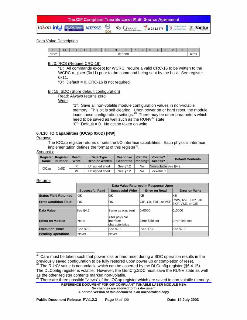
REFERENCE DOCUMENT FOR OIF COMPLIANT TUNABLE LASER MODULE MSA No changes are allowed to this document
A printed version of this document is an uncontrolled copy
Public Document Release PV:1.2.3 Page 63 of 120 Date: 14 July 2003
Data Value Description
15 14 13 12 11 10 9 8 7 6 5 4 3 2 1 0 SDC 0x0000 RCS
Bit 0: RCS (Require CRC-16)
“1”: All commands except for WCRC, require a valid CRC-16 to be written to the WCRC register (0x11) prior to the command being sent by the host. See register 0x11. “0”: Default = 0. CRC-16 is not required.
Bit 15: SDC (Store default configuration) Read: Always returns zero. Write:
“1”: Save all non-volatile module configuration values in non-volatile memory. This bit is self clearing. Upon power on or hard reset, the module loads these configuration settings.40 There may be other parameters which need to be saved as well such as the RUNV41 state. “0”: Default = 0. No action taken on write.
6.4.10 IO Capabilities (IOCap 0x0D) [RW] Purpose
The IOCap register returns or sets the I/O interface capabilities. Each physical interface implementation defines the format of this register42.
Synopsis: Register
Name Register Number
Read / Write
Data Type Read or Written
Response Generated
Can Be Pending?
Volatile? Access? Default Contents
R Unsigned short See §7.2 No Non-volatile See §4.2 IOCap 0x0D
W Unsigned short See §7.2 No Lockable 2
Returns Data Value Returned in Response Upon Successful Read Successful Write Error on Read Error on Write
Status Field Returned: OK OK XE XE
Error Condition Field: OK OK CIP, CII, EXF, or VSE RNW, RVE, CIP, CII, EXF, VSE, or CIE
Data Value: See §4.2 Same as was sent 0x0000 0x0000
Effect on Module None Alter physical interface characteristics
Error field set Error field set
Execution Time: See §7.2 See §7.2 See §7.2 See §7.2 Pending Operation: Never Never
40 Care must be taken such that power loss or hard reset during a SDC operation results in the previously saved configuration to be fully restored upon power up or completion of reset. 41 The RUNV value is non-volatile which can be asserted by the DLConfig register (§6.4.15). The DLConfig register is volatile. However, the GenCfg:SDC must save the RUNV state as well as the other register contents marked non-volatile. 42 There are three possible “views” of the IOCap register which are saved in non-volatile memory.

REFERENCE DOCUMENT FOR OIF COMPLIANT TUNABLE LASER MODULE MSA No changes are allowed to this document
A printed version of this document is an uncontrolled copy
Public Document Release PV:1.2.3 Page 64 of 120 Date: 14 July 2003
Detailed Description The register returns to its default when hardware reset is asserted or then module is powered on. The physical interface can only be selected during power on or during hardware reset. When an interface speed is reconfigured, the response packet for the IOCap command is returned to the host. The interface speed is then changed to the requested speed and then the IRDY* line is then re-asserted. The host can monitor the IRDY* line to determine when the interface is ready for a command packet at the new interface speed. Changes to the module configuration are performed while the laser is not carrying traffic. The IOCap configuration can be saved as module reset/power on defaults.
Data Value Description See §4.2Communication Interfaces for detailed information on the register fields and default values.

REFERENCE DOCUMENT FOR OIF COMPLIANT TUNABLE LASER MODULE MSA No changes are allowed to this document
A printed version of this document is an uncontrolled copy
Public Document Release PV:1.2.3 Page 65 of 120 Date: 14 July 2003
6.4.11 Extended Addressing Mode Registers (0x09-0x0B, 0x0E-0x10) [RW] Purpose
The predefined register set provides two sets of three registers each that are utilized for extended addressing. The first set (0x09-0x0B) is normally pre-configured by the module when the host reads from or writes to a register that supports AEA (automatic extended addressing) mode. The second set is normally pre-configured for large transfers such as a firmware upload or download. Note that two sets of extended address registers is desirable in case an AEA register needs to be accessed during a lengthy upload or download.
Synopsis: Register
Name Register Number
Read / Write
Data Type Read or Written
Response Generated
Can Be Pending?
Volatile? Access? Default Contents
R Unsigned short See §7.2 No 0x0000 AEA-EAC 0x09
W R Unsigned short See §7.2 No 0x0000
AEA-EA 0x0A W R See §7.2 No No Default Required
AEA-EAR 0x0B W
Defined by target field format See §7.2 Yes --
R Unsigned short See §7.2 No 0x0000 EAC 0x0E
W Unsigned short See §7.2 No Lockable 3 R Unsigned short See §7.2 No 0x0000
EA 0x0F W Unsigned short See §7.2 No Lockable 3 R See §7.2 No No Default Required
EAR 0x10 W
Defined by target field format See §7.2 Yes --
Returns Data Value Returned in Response Upon Successful Read Successful Write Error on Read Error on Write
Status Field Returned: OK OK XE XE
Error Condition Field: OK OK CIP, CII, ERE, EXF, or VSE
RNW, RVE, CIP, CII, ERE, ERO, EXF, or VSE
Data Value: See definitions below See definitions below 0x0000 0x0000
EAC, EA- None EAC, EA- ConfiguredEffect on Module EAR- EAC:EA
incremented EAR- Field written, EAC:EA incremented
Error field set Address unchanged
Error field set Address unchanged
Execution Time: See §7.2 See §7.2 See §7.2 See §7.2 Pending Operation: Never Yes43
Detailed Description
In order to access a location through the extended addressing interface, the EAC and EA registers must properly configured. This configuration occurs automatically when AEA designated registers are accessed or when the DLConfig process is initiated. Read or write access of a register that supports AEA returns the number of bytes in the field. The access also configures the AEA-EAC and AEA-EA registers. Subsequent reads
43 Note that writes to the AEA-EAR register or the EAR register may result a pending operation (CP flag) if a non-volatile memory “store” cycle takes longer than the 5ms execution time.

REFERENCE DOCUMENT FOR OIF COMPLIANT TUNABLE LASER MODULE MSA No changes are allowed to this document
A printed version of this document is an uncontrolled copy
Public Document Release PV:1.2.3 Page 66 of 120 Date: 14 July 2003
or writes on AEA-EAR transfers data sequentially from the physical or virtual memory location where the field is stored. Note that although a write to a register that supports AEA access returns the maximum number of bytes to be written, but no data is actually written. The write command must be re-issued to the AEA-EAR register in order to complete the write.
Operation on Register Which Support AEA
Data Value Sent Effect on AEA Data Value Returned
Read 0x0000 Configured Number of bytes in the previously stored value.
0x0000 NOT Configured
Maximum number of bytes that can be stored in the field. Write
Number of bytes to be stored in the coming AEA transfer.
Configured 0x0000
Reading or writing beyond the field boundaries will generate an execution error. An execution error on read or write does not increment the extended address register’s contents. A soft reset (ResEna 0x32) or a low to high transition of the MS* line will abort extended address transfers (firmware uploads or AEA transfers).
Data Value Description See the following sections.
6.4.11.1 Extended Address Configuration (EAC 0x09 & 0x0E) The first register, AEA-EAC (0x09) or EAC (0x0E), configures the extended addressing mode.
15 14 13 12 11 10 09 08 07 06 05 04 03 02 01 00
RAI WAI EAM INCR TBD High order 6 address bits RAI: Read Auto Increment (Bits 15:14)
0x0 No address change on read 0x1 Address auto post increment by INCR on read 0x2 Address auto post decrement by INCR on read 0x3 Action not defined
WAI: Write Auto Increment (Bits 13:12)
0x0 No address change on write 0x1 Address auto post increment by INCR on write 0x2 Address auto post decrement by INCR on write 0x3 Action not defined
EAM: Extended Address Mode (Bits 11:9)
These three bits provide 8 possible address spaces. The default register space is defined with EAM=0x0. A firmware upgrade procedure would select the appropriate “code address

REFERENCE DOCUMENT FOR OIF COMPLIANT TUNABLE LASER MODULE MSA No changes are allowed to this document
A printed version of this document is an uncontrolled copy
Public Document Release PV:1.2.3 Page 67 of 120 Date: 14 July 2003
space”.
Table 6.4-1 Extended Address Space Mode Selection (EAM) EAM Address Space 0x0 Default register space (including 0x00 – 0xff) 0x1 Physical data space 1 0x2 Physical data space 2 0x3 Physical code space 1 0x4 Physical code space 2
0x5-0x7 Manufacturer specific INCR: Increment register (Bits 8:7)
The auto increment and auto decrement operations modify the address by this unsigned value. For register space, this would typically be 1. If the physical space addressed by bytes, the best increment might more naturally be 2. If the configuration transfers 1 byte per read or write, only the low order byte is transferred and the high order byte is ignored.
TBD: Reserved (Bit 6) High order address bits: (Bits 5:0)
The high order address bits are concatenated with the EA register forming a 22 bit physical or logical address or register number.
6.4.11.2 Extended Address (EA 0x0A & 0x0F) The second register, EA, contains the lower 16 address bits.
15 14 13 12 11 10 9 8 7 6 5 4 3 2 1 0 Extended Address (low order16 bits)
This register is set to the address value. Note with EAM=0x0, this register accesses the default register space. With EAM=0x0, extended addresses from 0x00 to 0xFF are equivalent to registers 0x00 to 0xFF.
6.4.11.3 Extended Address Access Register (EAR 0x0B & 0x10)
A read on EAR causes the value referred to by EAC:EA to be returned. A write to EAR causes the location referred to by EAC:EA to be written, assuming the register is write-able.
15 14 13 12 11 10 9 8 7 6 5 4 3 2 1 0 Contents of Extended Address
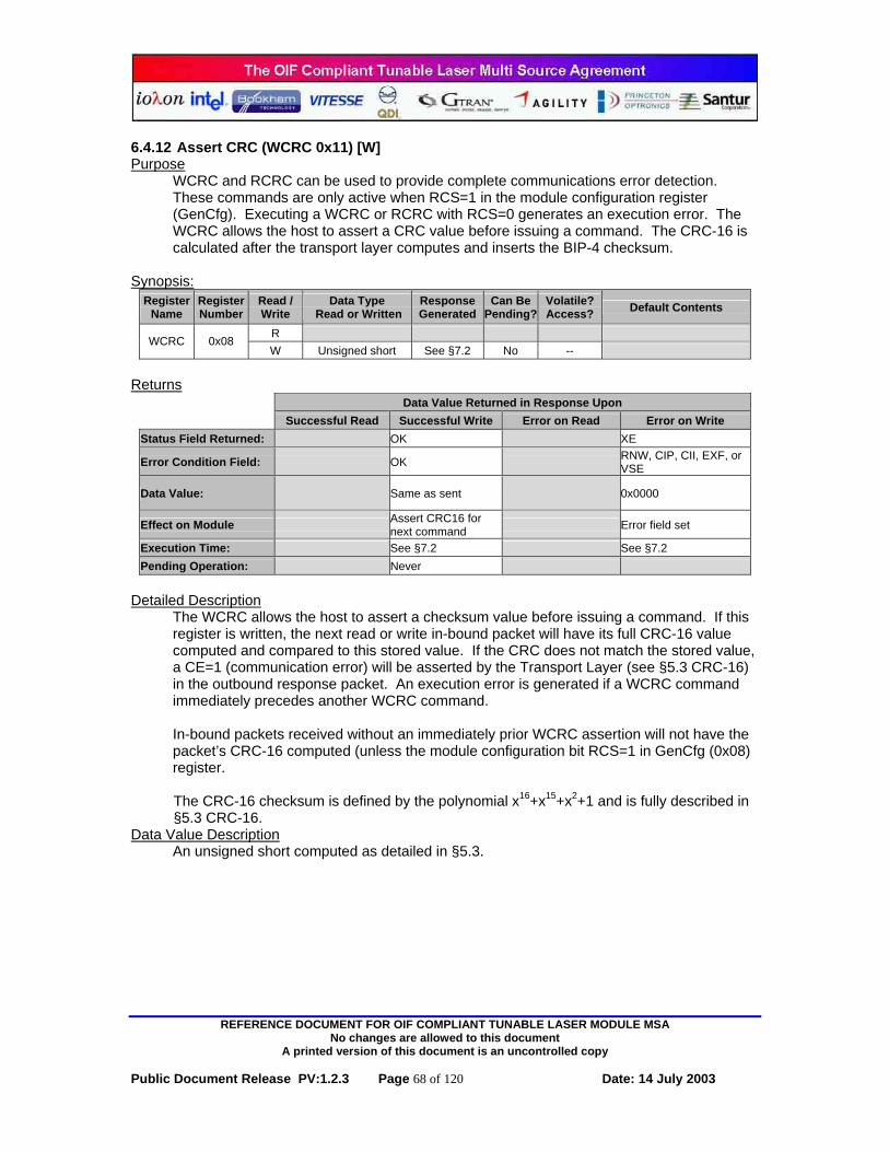
REFERENCE DOCUMENT FOR OIF COMPLIANT TUNABLE LASER MODULE MSA No changes are allowed to this document
A printed version of this document is an uncontrolled copy
Public Document Release PV:1.2.3 Page 68 of 120 Date: 14 July 2003
6.4.12 Assert CRC (WCRC 0x11) [W] Purpose
WCRC and RCRC can be used to provide complete communications error detection. These commands are only active when RCS=1 in the module configuration register (GenCfg). Executing a WCRC or RCRC with RCS=0 generates an execution error. The WCRC allows the host to assert a CRC value before issuing a command. The CRC-16 is calculated after the transport layer computes and inserts the BIP-4 checksum.
Synopsis:
Register Name
Register Number
Read / Write
Data Type Read or Written
Response Generated
Can Be Pending?
Volatile? Access? Default Contents
R WCRC 0x08
W Unsigned short See §7.2 No --
Returns Data Value Returned in Response Upon Successful Read Successful Write Error on Read Error on Write
Status Field Returned: OK XE
Error Condition Field: OK RNW, CIP, CII, EXF, or VSE
Data Value: Same as sent 0x0000
Effect on Module Assert CRC16 for next command Error field set
Execution Time: See §7.2 See §7.2 Pending Operation: Never
Detailed Description
The WCRC allows the host to assert a checksum value before issuing a command. If this register is written, the next read or write in-bound packet will have its full CRC-16 value computed and compared to this stored value. If the CRC does not match the stored value, a CE=1 (communication error) will be asserted by the Transport Layer (see §5.3 CRC-16) in the outbound response packet. An execution error is generated if a WCRC command immediately precedes another WCRC command. In-bound packets received without an immediately prior WCRC assertion will not have the packet’s CRC-16 computed (unless the module configuration bit RCS=1 in GenCfg (0x08) register. The CRC-16 checksum is defined by the polynomial x16+x15+x2+1 and is fully described in §5.3 CRC-16.
Data Value Description An unsigned short computed as detailed in §5.3.
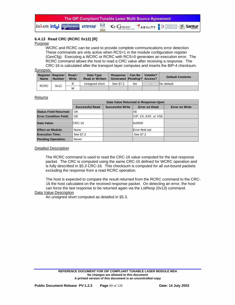
REFERENCE DOCUMENT FOR OIF COMPLIANT TUNABLE LASER MODULE MSA No changes are allowed to this document
A printed version of this document is an uncontrolled copy
Public Document Release PV:1.2.3 Page 69 of 120 Date: 14 July 2003
6.4.13 Read CRC (RCRC 0x12) [R] Purpose
WCRC and RCRC can be used to provide complete communications error detection. These commands are only active when RCS=1 in the module configuration register (GenCfg). Executing a WCRC or RCRC with RCS=0 generates an execution error. The RCRC command allows the host to read a CRC value after receiving a response. The CRC-16 is calculated after the transport layer computes and inserts the BIP-4 checksum.
Synopsis: Register
Name Register Number
Read / Write
Data Type Read or Written
Response Generated
Can Be Pending?
Volatile? Access? Default Contents
R Unsigned short See §7.2 No -- No default RCRC 0x12
W
Returns Data Value Returned in Response Upon Successful Read Successful Write Error on Read Error on Write
Status Field Returned: OK XE Error Condition Field: OK CIP, CII, EXF, or VSE
Data Value: CRC-16 0x0000
Effect on Module None Error field set Execution Time: See §7.2 See §7.2 Pending Operation: Never
Detailed Description
The RCRC command is used to read the CRC-16 value computed for the last response packet. The CRC is computed using the same CRC-16 defined for WCRC operation and is fully described in §5.3 CRC-16. This checksum is computed for all out-bound packets excluding the response from a read RCRC operation. The host is expected to compare the result returned from the RCRC command to the CRC-16 the host calculated on the received response packet. On detecting an error, the host can force the last response to be returned again via the LstResp (0x13) command.
Data Value Description An unsigned short computed as detailed in §5.3.

REFERENCE DOCUMENT FOR OIF COMPLIANT TUNABLE LASER MODULE MSA No changes are allowed to this document
A printed version of this document is an uncontrolled copy
Public Document Release PV:1.2.3 Page 70 of 120 Date: 14 July 2003
6.4.14 Last Response (LstResp 0x13) [R] Purpose
WCRC, RCRC and LstResp can be used to provide complete communications error detection. Reading last response register forces the module to return all four bytes of the last non-RCRC response. This is useful if a CRC-16 or checksum error was detected and the host wants to re-read the last response. Upon completion, the RCRC register contains the same CRC-16 value it had before the register was read. This register is active whether or not RCS=1 in the module configuration register.
Synopsis: Register
Name Register Number
Read / Write
Data Type Read or Written
Response Generated
Can Be Pending?
Volatile? Access? Default Contents
R Last Response See §7.2 No Last Response LstResp 0x13
W
Returns Data Value Returned in Response Upon Successful Read Successful Write Error on Read Error on Write
Status Field Returned: OK XE Error Condition Field: OK CIP, CII, EXF, or VSE
Data Value: Last Response 0x0000
Effect on Module None Error field set Execution Time: See §7.2 See §7.2 Pending Operation: Never
Detailed Description Note that the RCRC is the only command who’s response doesn’t affect the value of the LstResp register.
Data Value Description Note that the entire out-bound packet is returned including all flag values.
Example Usage
Command (Host to Module) Response (Module to Host) # Operation Register
Data Bytes (15:0)
Status Register Data Bytes (15:0)
Read 0x00 (NOP) 0x0000 0x00 (Ok) 0xFF (garbled!!) 0x0000 1 Note: Example showing garbled response, CRC and/or checksum indicate error in receipt of response. 2 Read 0x13 (LstResp) 0x0000 0x00 (Ok) 0x00 (NOP) 0x0100 Note: The module’s last response is transmitted again and this time received correctly.

REFERENCE DOCUMENT FOR OIF COMPLIANT TUNABLE LASER MODULE MSA No changes are allowed to this document
A printed version of this document is an uncontrolled copy
Public Document Release PV:1.2.3 Page 71 of 120 Date: 14 July 2003
6.4.15 Download Configuration (DLConfig 0x14) [RW] Purpose
The DLConfig register configures a host to module download of code or data for reconfiguration purposes or configures a module to host upload of code or data to the host. A file transfer may occur at several locations such as vendor factory, customer site (on the bench), customer system (circuit down), or potentially a customer system (live circuit).
Synopsis: Register
Name Register Number
Read / Write
Data Type Read or Written
Response Generated
Can Be Pending?
Volatile? Access? Default Contents
R Unsigned short See §7.2 No 0x0000 | RUNV<<8 DLConfig 0x14
W Unsigned short See §7.2 Yes Lockable 2
Returns Data Value Returned in Response Upon Successful Read Successful Write Error on Read Error on Write
Status Field Returned: OK OK XE XE
Error Condition Field: OK OK CIP, CII, EXF, or VSE RNW, RVE, CIP, CII, EXF, CIE, or VSE
Data Value: DL Configuration Same as sent 0x0000 0x0000
Effect on Module None
Down Load configured, check initiated, or RUNV execution selected
Error field set Error field set
Execution Time: See §7.2 See §7.2 See §7.2 See §7.2 Pending Operation: Never Yes
Detailed Description
The following example describes the actions required to transfer a file from the host to the module and then have the module run that file.
Table 6.4.15-1 Firmware Download Example Step Host Sends Module Responds
1
Write the DLConfig register indicating the type of transfer coming and asserting INIT_WRITE=1 and TYPE. Code might be boot code, run time code, FPGA code, CPLD code.
Module responds by initializing extended address registers (0x0E-0x0F) and may return a pending operation flag if pre-configuration will take longer than the allowed response time (§7.2).
2 Host writes to the extended address register (0x10) with the file data, 2 bytes at a time.
Module receives file data 2 bytes at a time and asserts a pending operation flag as necessary. Each out-bound packet response indicates if any errors have occurred.
3 Host writes DLConfig and asserts DONE=1. Module completes transfer and performs any clean-up operations related to the write sequence. The module may respond with a pending operation flag.
4 Host writes DLConfig and asserts INIT_CHECK=1
The module performs the consistency check and sets the VALID bit accordingly in DLStatus. The module may respond with a pending operation flag.
5 Host reads DLStatus and checks for VALID=1 Modules responds with the DLStatus information
6 Host writes DLConfig with INIT_RUN=1 and asserts RUNV set to the same value as TYPE in step 1.
Module either (1) responds and is running the new requested code segment or (2) the module responds with a pending operation flag and begins the process of running the requested code segment.

REFERENCE DOCUMENT FOR OIF COMPLIANT TUNABLE LASER MODULE MSA No changes are allowed to this document
A printed version of this document is an uncontrolled copy
Public Document Release PV:1.2.3 Page 72 of 120 Date: 14 July 2003
Table 6.4.15-2 Firmware Upload Example Step Host Sends Module Responds
1
Write the DLConfig register indicating the type of transfer coming and asserting INIT_READ=1 and TYPE. Code might be boot code, run time code, FPGA code, CPLD code.
Module responds by initializing extended address registers (0x0E-0x0F) and may return a pending operation flag if pre-configuration will take longer than the allowed response time (§7.2).
2 Host reads from the extended address register (0x10), 2 bytes at a time.
Module sends file data 2 bytes at a time. Each out-bound packet response indicates if any errors have occurred.
Data Value Description
When the DLConfig register is read, the RUNV value returns the value for the firmware currently running in the module. This value is unchanged with a power down or reset. The other fields return the default values.
15 14 12 12 11 10 9 8 TYPE RUNV
7 6 5 4 3 2 1 0 Reserved
(0x0) INIT_RUN INIT_CHECK INIT_READ DONE ABRT INIT_WRITE
INIT_WRITE Bit 0
This bit informs the module to prepare for download and may result in a pending operation. The module should perform its necessary housekeeping to be ready for download. Pre-configures the extended address registers (0x0E-0x0F).
0 – Do not start download. (default) 1 – Prepare for download. (May result in a pending operation)
ABRT Bit 1
This bit informs the module to abort the transfer and may result in a pending operation.
0 – Do not abort transfer. (default) 1 – Abort the transfer. (May result in a pending operation)
DONE Bit 2
This bit informs the module that the transfer is complete and may result in a pending operation. 0 – Transfer is not done. (default) 1 – Transfer is done. (May result in a pending operation)
INIT_READ Bit 3
This bit informs the module to prepare for upload and may result in a pending operation. Like INIT_WRITE, this pre-configures the extended address registers (0x0E- 0x0F). 0 – Do not start upload. (default) 1 – Prepare for upload (May result in a pending operation)

REFERENCE DOCUMENT FOR OIF COMPLIANT TUNABLE LASER MODULE MSA No changes are allowed to this document
A printed version of this document is an uncontrolled copy
Public Document Release PV:1.2.3 Page 73 of 120 Date: 14 July 2003
INIT_CHECK Bit 4 This bit, when set to “1”, instructs the module to check the segment specified in the TYPE field for consistency and may result in a pending operation. Upon completion, the DLStatus (0x015) register’s VALID bit is set to “1” or set to “0” to indicate if the segment is valid. 0 – Do not initiate consistency check. (default) 1 – Initiate consistency check (May result in a pending operation)
INIT_RUN Bit 5 This bit, when set to “1”, informs the module to run the segment specified in the RUNV field. The module will transmit a response packet. The request may result in a pending operation if the time to begin execution of the requested code segment will take longer than the maximum time for the module to construct a response44. (See §7.2) 0 – Do not run code specified by RUNV. (default) 1 – Run code specified by RUNV (May result in a pending operation)
RUNV – Bit 8-11 Specifies version to run when written with a non-zero value and with INIT_RUN=1. Returns the current version that is currently executing when read. The default setting is vendor specific. Vendors may not support all RUNV values. A RUNV value which contains a code segment with an invalid an internal CRC check on that code segment will return a execution error (EXF).
TYPE Value Code Type Effect on Module
0x00 No change to value None 0x01 FW Version A1 Non-Service interrupting 0x02 FW Version B1 Non-Service interrupting 0x03 FW Version A2 Service Interrupting 0x04 FW Version B2 Service Interrupting
0x05-0x08 Reserved 0x09 – 0xFE Vendor specific
0xFF Reserved
44 There may be a short period of time during the pending operation when it will not respond to commands form the host.

REFERENCE DOCUMENT FOR OIF COMPLIANT TUNABLE LASER MODULE MSA No changes are allowed to this document
A printed version of this document is an uncontrolled copy
Public Document Release PV:1.2.3 Page 74 of 120 Date: 14 July 2003
TYPE Bit 12-15 Type of code to Transfer (0x0 – default)
TYPE Value Code Type Effect on Module
0x0 No change to value None 0x1 FW Version A1 0x2 FW Version B1 Non-Service interrupting45
0x3 FW Version A2 0x4 FW Version B2 Service Interrupting46
0x5-0x8 Reserved 0x9 – 0xE Vendor specific
0xF Reserved 6.4.16 Download Status (DLStatus 0x15) [R] Purpose
DLStatus provides information about the status or viability of a code segment.
Synopsis: Register
Name Register Number
Read / Write
Data Type Read or Written
Response Generated
Can Be Pending?
Volatile? Access? Default Contents
R Unsigned short See §7.2 No Defined upon write to DLConfig DLStatus 0x08
W
Returns Data Value Returned in Response Upon Successful Read Successful Write Error on Read Error on Write
Status Field Returned: OK XE Error Condition Field: OK CIP, CII, EXF, or VSE
Data Value: Defined upon write to DLConfig 0x0000
Effect on Module None Error field set Execution Time: See §7.2 See §7.2 Pending Operation: Never
Detailed Description
The register provides information on the polling sequence that should be used during the configured download (see §6.4.15) as well as the status of the download.
45 The primary firmware is generally loaded and executed without interrupting traffic (A1, B1). However, there may be technologies for which the firmware download may be service interrupting and would be loaded in slots A2, B2. 46 A DLConfig write to initiate a service interrupting download while the module’s output is enabled is not allowed and an execution error is returned (CIE).

REFERENCE DOCUMENT FOR OIF COMPLIANT TUNABLE LASER MODULE MSA No changes are allowed to this document
A printed version of this document is an uncontrolled copy
Public Document Release PV:1.2.3 Page 75 of 120 Date: 14 July 2003
Data Value Description
15 14 13 12 11 10 9 8 7 6 5 4 3 2 1 0 IN_USE VALID
VALID Bit 0
Indicates that the module has a valid code type at this location. Asserted after the DLConfig (0x14) “TYPE” field is written with a non-zero type field. 0 – Indicates that the module does not have a valid code type at this location. 1 – Indicates that the module does have a valid code type at this location.
IN_USE Bit 1
Can be used to indicate that the code type specified in the DLConfig (0x14) “TYPE” field is currently in use. 0 – Indicates that segment is not currently in use 1 – Indicates that segment is currently in use
6.4.17 Register Lockout (Lock 0x16) [RW] Purpose:
Lock provides a mechanism to restrict write access to certain registers. Registers with the “Lockable” attribute will be unlocked when the Lock register is written with the appropriate value. The locking function is enabled by writing a sequence of unsigned chars to the Lock register through AEA access. Full register lock out is accomplished by writing a single byte 0x00 to the field referenced by the Lock register’s configuration of the AEA register.
Synopsis: Register
Name Register Number
Read / Write
Data Type Read or Written
Response Generated
Can Be Pending?
Volatile? Access? Default Contents
R Lock 0x16
W
0x00XX AEA (Array of unsigned char) See §7.2 Yes Lock level 1
Returns Data Value Returned in Response Upon Successful Read Successful Write Error on Read Error on Write
Status Field Returned: OK XE
Error Condition Field: OK RNW, RVE, CIP, CII, EXF, or VSE
Data Value: 0xPP00 (pending operation field) 0x0000
Effect on Module
AEA registers configured to reference array Lock level set.
Error field set
Execution Time: See §7.2 See §7.2 Pending Operation: Yes
Detailed Description
Read access is not allowed for the Lock register.

REFERENCE DOCUMENT FOR OIF COMPLIANT TUNABLE LASER MODULE MSA No changes are allowed to this document
A printed version of this document is an uncontrolled copy
Public Document Release PV:1.2.3 Page 76 of 120 Date: 14 July 2003
Writing a 0x0000 to Lock (0x16) will return the maximum field size for the write. Unlocking the registers requires writing an integer array (a key) to the Lock register through the AEA mechanism. The write is initiated by sending the number of bytes to be written in the write command. The module responds with a pending operation indicating that the write will be pending transfer of desired bytes to be written. Once the intended number of bytes has been written, the pending operation is completed. If the key matches the module’s unlock criteria, the associated registers will be unlocked. The value of the lock level can be read via the NOP/Status (0x00) register. The values (of the key) that unlocks the registers for a non-zero lock level is manufacturer specific. The value that write-locks all the registers (except write access to the lock register) is the single byte 0x00. Writing invalid key values to the Lock register field results in an execution error (RVE). The default value of the configured lockout level is configurable and can be changed via the GenCfg:SDC operation. The current lock level can be read via the NOP/Status register. See §6.4.1.
Data Value Description Manufacturers may implement keys of any length from 2 to 20 bytes in length.
Table 6.4-3: Register Lockout Lock Levels Lock Level Description Key Value Key Length
0 Fully locked (all lockable registers are write protected 0x0 1
1 Partially unlocked – Lockable registers 1 are unlocked Available for channel tuning etc. MFG Specific <20
2 Partially unlocked – Lockable registers 2 are unlocked Available for Reset, firmware uploads, alarm thresholds (Basic module configuration)
MFG Specific <20
3 All lockable registers are unlocked Normally reserved for manufacturer use. MFG Specific <20

REFERENCE DOCUMENT FOR OIF COMPLIANT TUNABLE LASER MODULE MSA No changes are allowed to this document
A printed version of this document is an uncontrolled copy
Public Document Release PV:1.2.3 Page 77 of 120 Date: 14 July 2003
6.5 Module Status Commands
6.5.1 StatusF, StatusW (0x20, 0x21) [RW] Purpose
The StatusF and StatusW commands return the tunable laser status upon a read and provide a way to clear status flags on a write. There are two status registers, one that primarily indicates FATAL conditions (0x20) and the other that primarily indicates WARNING conditions (0x21).
Synopsis:
Register Name
Register Number
Read / Write
Data Type Read or Written
Response Generated
Can Be Pending?
Volatile? Access? Default Contents
R Unsigned short See §7.2 No 0x0000 StatusF 0x20
W Typically 0x00FF See §7.2 No -- R Unsigned short See §7.2 No 0x0000
StatusW 0x21 W Typically 0x00FF See §7.2 No --
Returns
Data Value Returned in Response Upon Successful Read Successful Write Error on Read Error on Write
Status Field Returned: OK OK XE XE Error Condition Field: OK OK CIP, CII, EXF, or VSE CIP, CII, EXF, or VSE
Data Value: Status value Same as sent (0x00FF) 0x0000 0x0000
Effect on Module None Clear the corresponding flags where bit=1
Error field set Error field set
Execution Time: See §7.2 See §7.2 See §7.2 See §7.2 Pending Operation: Never Never
Detailed Description
The fatal and warning flags have both a latched representation and a non-latched representation. The latched versions of the flags remain set even if the transient condition expires. The fatal and warning flags are available.
FATAL Conditions Warning Conditions Condition Latching Non-Latching Latching Non-Latching Thermal FTHERML FTHERM WTHERML WTHERM Output Power FPWRL FPWR WPWRL WPWR Frequency FFREQL FFREQ WFREQL WFREQ Vendor Specific Fault FVSFL FVSF WVSFL WVSF
Fatal flags indicate a serious failure in the tunable laser typically result in optical output shutdown to avoid interference with other channels. Module behavior due to fatal conditions is specified in register MCB (0x33), bit SDF. Fatal conditions vary with laser technology but might be a result of one of the following:
Gross loss of thermal control primarily impacting frequency and/or output power control of the module. An example would be an inability to determine frequency accurately due to loss of thermal control. The control set point is defined by the manufacturer and the control limits are specified in register FThermTh (0x26).

REFERENCE DOCUMENT FOR OIF COMPLIANT TUNABLE LASER MODULE MSA No changes are allowed to this document
A printed version of this document is an uncontrolled copy
Public Document Release PV:1.2.3 Page 78 of 120 Date: 14 July 2003
Gross loss of optical output power control to within the required tolerance contained in the FPowTh (0x22) register.
Gross loss of frequency control to within the required tolerance contained in the FFreqTh (x024) register.
Other vendor specific fatal conditions determined by technology choice. Warning flags indicate non-fatal conditions in the module and will not cause shutdown. Warning conditions may be precursors to eventual fatal failure. Warning conditions vary with laser technology. The following list contains only some of the possible conditions resulting in a warning. See manufacturer’s documentation for a complete list.
Thermal o Module’s case temperature exceeds control limits set by TCaseL and
TCaseH (0x5D-5E) o Module’s internal thermal control is marginal. Control limits set by
WThermTh (0x27) Power – (Control limits set by WpowTh) (0x23) Frequency – (Control limits set by WfreqTh) (0x25) Other vendor specific warning conditions determined by technology choice.
The latched flags are cleared by writing a “1” to the corresponding bit position. Typically, the latched bits are cleared by writing a 0x00FF to each register (0x20, 0x21). Clearing the latched bits will cause de-assertion of the corresponding hardware line (FATAL* and/or SRQ*). If the condition is still occurring, the corresponding latched bit will be set back to “1” triggering re-assertion of the corresponding hardware lines.
Data Value Description
0x20 Current Status (Fatal) – Read Only
15 14 13 12 11 10 9 8 SRQ ALM FATAL DIS FVSF FFREQ FTHERM FPWR
0x20 Latched Status (Fatal) – RW
7 6 5 4 3 2 1 0 XEL CEL MRL CRL FVSFL FFREQL FTHERML FPWRL
0x21 Current Status (Warning) – Read Only
15 14 13 12 11 10 9 8 SRQ ALM FATAL DIS WVSF WFREQ WTHERM WPWR
0x21 Latched Status (Warning) – RW
7 6 5 4 3 2 1 0 XEL CEL MRL CRL WVSFL WFREQL WTHERML WPWRL
The other status flags are defined as follows:
Condition Latched Flag Non-Latching Flag SRQ* asserted None SRQ ALM* asserted None ALM FATAL* asserted None FATAL DIS* asserted None DIS Execution error asserted XEL XE flag in out-bound byte 0 Communications error asserted CEL CE flag in out-bound byte 0 Module Reset asserted MRL None CR asserted CRL None

REFERENCE DOCUMENT FOR OIF COMPLIANT TUNABLE LASER MODULE MSA No changes are allowed to this document
A printed version of this document is an uncontrolled copy
Public Document Release PV:1.2.3 Page 79 of 120 Date: 14 July 2003
Bits 15:8 in the status registers are non-latching and indicate the current module condition. These bits cannot be cleared. Writing to these bits (0xFF00) does not cause an error. Bits 7:0 are latching and indicate whether any of the conditions that have occurred since the last time the status registers were cleared. These bits can be cleared by writing a 0x00FF to the status registers. Bit 15: SRQ – Service Request Bit (read –only) (default 0)
The SRQ bit is read only. It reflects the state of the module’s SRQ* line. When the SRQ* line is asserted (low or zero), this bit is set to 1. The SRQ* line is fully configurable through the SRQ* trigger register 0x28.
Bit 14: ALM – ALARM Flag bit (read-only) (default 0)
The ALM bit is read only. It reflects the state of the module’s ALM* line. When the ALM* line is asserted (low or zero), this bit is set to 1. The conditions which set the ALM* line are fully configurable through the alarm trigger register (0x2A).
Bit 13: FATAL – FATAL alarm bit (read-only) (default 0)
The FATAL bit is read only. It reflects the state of the module’s FATAL* line. When the FATAL* line is asserted (low or zero), this bit is set to 1. The conditions which set the FATAL* line are fully configurable through the fatal trigger register (0x29).
Bit 12: DIS – Module’s output is hardware disabled (read-only)
The module’s laser output disable bit is read only and represents the state of the hardware disable pin (DIS*). When set to one, the module is “hardware” disabled. When the DIS* pin is set to zero, the SENA bit is also cleared. Therefore when DIS* is set to one, the module does not re-enable the output until the SENA is also set. Any state change in DIS can cause SRQ* to be asserted if the appropriate SRQ* trigger is set.47
1: Module disabled (DIS* line is low) 0: DIS* line is high
Bit 11: FVSF, WVSF – Vendor Specific Fault (read-only) (default 0)
The FVSF bit (0x20) is set to 1 whenever a fatal vendor specific condition is asserted. The WVSF bit (0x21) is set to 1 whenever a warning vendor specific condition is asserted. If either of these bits are set, the vendor will have a register defined which contains vendor specific fault conditions.
Bit 10: FFREQ & WFREQ – Frequency Fatal and Warning (read-only) (default 0)
The FFREQ bit (0x20) reports that the frequency deviation has exceeded the frequency fatal threshold (0x24) while WFREQ bit (0x21) reports that the frequency deviation has exceeded the frequency warning threshold (0x25).
47 The operation ensures that a tuning operation only occurs under s/w control. The primary purpose of the DIS* pin is to rapidly disable the laser output. In some implementations, the tuning command can make the module de-assert IRDY* during the tuning command. The behavior of clearing the SENA bit allows the IRDY* line to be solely activated by software transfers and simplifies possible sources of confusion.

REFERENCE DOCUMENT FOR OIF COMPLIANT TUNABLE LASER MODULE MSA No changes are allowed to this document
A printed version of this document is an uncontrolled copy
Public Document Release PV:1.2.3 Page 80 of 120 Date: 14 July 2003
When bit 10 is 1, it indicates that the frequency deviation threshold is being exceeded. When bit 10 is 0, the frequency deviation threshold is not being exceeded.
Bit 9: FTHERM & WTHERM – Thermal Fatal and Warning (read-only) (default 0)
The FTHERM bit (0x20) reports that the thermal deviation has exceeded the thermal fatal threshold (0x26) while WTHERM bit (0x21) reports that the thermal deviation has exceeded the thermal warning threshold (0x27). When bit 9 is 1, it indicates that the thermal deviation threshold is being exceeded. When bit 9 is 0, the thermal deviation threshold is not being exceeded.
Bit 8: FPWR & WPWR – Power Fatal and Warning (read-only) (default 0)
The FPWR bit (0x20) reports that the power deviation has exceeded the power fatal threshold (0x22) while WPWR bit (0x21) reports that the power deviation has exceeded the power warning threshold (0x23). When bit 8 is 1, it indicates that the power deviation threshold is being exceeded. When bit 8 is 0, the power deviation threshold is not being exceeded.
Bit 7: XEL – Flags an execution error.
A “1” indicates an exceptional condition. Note that execution errors could be generated by a command just given which failed to execute as well as a command that was currently executing (a pending operation that just complete). The XE bit remains set until cleared.
Bit 6: CEL – Flags a communication error.
A “1” indicates a communication error. The CE bit remains set until cleared. Bit 5: MRL – Module Restarted (latched) (read-only) (default 1 – by definition)
The MRL bit is read only. When it is set, it indicates that the module has been restarted either by power up, by hardware or software reset, or by a firmware mandated restart. Depending upon the implementation, this may indicate that the laser’s output signal may be invalid. Note that the module can be reset through the communication interface by writing to register 0x32. The bit remains set until cleared.
Bit 4: CRL – Communication Reset (latched) (read-only) (default 1 – by definition)
The CRL bit is read only. When it is set, it indicates that the module has undergone a communication interface reset. The input buffers were cleared. This can also occur after a manufacturer specific timeout period has elapsed in the middle of a packet transfer.48 The bit remains set until cleared.
Bits 3,2,1,0: FVSFL, FFREQL, FTHERML, FPWRL, WVSFL, WFREQL, WTHERML,
WPWRL – Latched fatal and warning indicators (RW) (default 0) These flags are latched versions of bits 11-8 for the fatal and warning threshold deviations. These bit indicators can be clearfed by writing a “1” to these bit positions.
48 Added reference to the capability of a communication interface timeout which would occur if a packet transfer didn’t complete. The timeout would be manufacturer specific.

REFERENCE DOCUMENT FOR OIF COMPLIANT TUNABLE LASER MODULE MSA No changes are allowed to this document
A printed version of this document is an uncontrolled copy
Public Document Release PV:1.2.3 Page 81 of 120 Date: 14 July 2003
When any of these bits is 1, it indicates that the corresponding deviation threshold has been exceeded at sometime in past (since the last clear) and may still be occurring. When any of these bits are “0”, the corresponding deviation threshold has not occurred since the last clear.
6.5.2 Power Threshold (FPowTh, WPowTh 0x22, 0x23) [RW] Purpose
FPowTh specifies the maximum power deviation ±dB at which the fatal alarm is asserted. WPowTh specifies the maximum power deviation ±dB at which the warning alarm is asserted.
Synopsis: Register
Name Register Number
Read / Write
Data Type Read or Written
Response Generated
Can Be Pending?
Volatile? Access? Default Contents
R See §7.2 No Non-volatile Manufacturer specific FPowTh 0x22
W Unsigned short
dB*100 See §7.2 No Lockable 2 R See §7.2 No Non-volatile Manufacturer specific
WPowTh 0x23 W
Unsigned short dB*100 See §7.2 No Lockable 2
Returns
Data Value Returned in Response Upon Successful Read Successful Write Error on Read Error on Write
Status Field Returned: OK OK XE XE
Error Condition Field: OK OK CIP, CII, EXF, or VSE RNW, RVE, CIP, CII, EXF, or VSE
Data Value: dB*100 dB*100 (Same as sent) 0x0000 0x0000
Effect on Module None New tolerance takes effect Error field set Error field set
Execution Time: See §7.2 See §7.2 See §7.2 See §7.2 Pending Operation: Never Never
Detailed Description
The value is stored in dB*100 as an unsigned integer. Setting a value outside of the usable range causes an execution error. The default is manufacturer specific and can be modified when the module configuration is stored in non-volatile memory.
Data Value Description The value is stored in dB*100 as an unsigned integer. The warning threshold (0x23) should typically be equal to or less than the value in register 0x22.

REFERENCE DOCUMENT FOR OIF COMPLIANT TUNABLE LASER MODULE MSA No changes are allowed to this document
A printed version of this document is an uncontrolled copy
Public Document Release PV:1.2.3 Page 82 of 120 Date: 14 July 2003
6.5.3 Frequency Threshold (FFreqTh, WFreqTh 0x24, 0x25) [RW] Purpose
FFreqTh specifies the maximum frequency deviation ±GHz at which the fatal alarm is asserted. WFreqTh specifies the maximum frequency deviation ±GHz at which the warning alarm is asserted.
Synopsis: Register
Name Register Number
Read / Write
Data Type Read or Written
Response Generated
Can Be Pending?
Volatile? Access? Default Contents
R See §7.2 No Non-volatile Application specific FFreqTh 0x24
W Unsigned short
±GHz*10 See §7.2 No Lockable 2 R See §7.2 No Non-volatile Application specific
WFreqTh 0x25 W
Unsigned short ±GHz*10 See §7.2 No Lockable 2
Returns
Data Value Returned in Response Upon Successful Read Successful Write Error on Read Error on Write
Status Field Returned: OK OK XE XE
Error Condition Field: OK OK CIP, CII, EXF, or VSE RNW, RVE, CIP, CII, EXF, or VSE
Data Value: ±GHz*10 ±GHz*10 (Same as sent) 0x0000 0x0000
Effect on Module None New tolerance takes effect Error field set Error field set
Execution Time: See §7.2 See §7.2 See §7.2 See §7.2 Pending Operation: Never Never
Detailed Description
The value is stored in GHz*10 as an unsigned integer. Setting a value outside of the usable range causes the value to be set to the maximum allowed. The default is manufacturer specific and can be modified when the module configuration is stored in non-volatile memory.
Data Value Description The value is stored in GHz*10 as an unsigned integer. The warning threshold (0x25) should typically be equal to or less than the value in register 0x24. Setting a value outside of the usable range generates an execution error. The default is application specific.
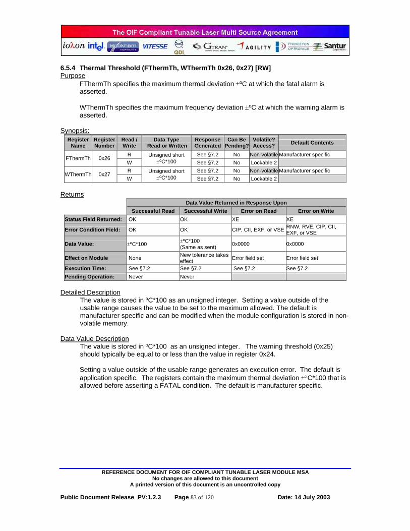
REFERENCE DOCUMENT FOR OIF COMPLIANT TUNABLE LASER MODULE MSA No changes are allowed to this document
A printed version of this document is an uncontrolled copy
Public Document Release PV:1.2.3 Page 83 of 120 Date: 14 July 2003
6.5.4 Thermal Threshold (FThermTh, WThermTh 0x26, 0x27) [RW] Purpose
FThermTh specifies the maximum thermal deviation ±ºC at which the fatal alarm is asserted. WThermTh specifies the maximum frequency deviation ±ºC at which the warning alarm is asserted.
Synopsis: Register
Name Register Number
Read / Write
Data Type Read or Written
Response Generated
Can Be Pending?
Volatile? Access? Default Contents
R See §7.2 No Non-volatile Manufacturer specific FThermTh 0x26
W Unsigned short
±ºC*100 See §7.2 No Lockable 2 R See §7.2 No Non-volatile Manufacturer specific
WThermTh 0x27 W
Unsigned short ±ºC*100 See §7.2 No Lockable 2
Returns
Data Value Returned in Response Upon Successful Read Successful Write Error on Read Error on Write
Status Field Returned: OK OK XE XE
Error Condition Field: OK OK CIP, CII, EXF, or VSE RNW, RVE, CIP, CII, EXF, or VSE
Data Value: ±ºC*100 ±ºC*100 (Same as sent) 0x0000 0x0000
Effect on Module None New tolerance takes effect Error field set Error field set
Execution Time: See §7.2 See §7.2 See §7.2 See §7.2 Pending Operation: Never Never
Detailed Description
The value is stored in ºC*100 as an unsigned integer. Setting a value outside of the usable range causes the value to be set to the maximum allowed. The default is manufacturer specific and can be modified when the module configuration is stored in non-volatile memory.
Data Value Description The value is stored in ºC*100 as an unsigned integer. The warning threshold (0x25) should typically be equal to or less than the value in register 0x24. Setting a value outside of the usable range generates an execution error. The default is application specific. The registers contain the maximum thermal deviation ±°C*100 that is allowed before asserting a FATAL condition. The default is manufacturer specific.

REFERENCE DOCUMENT FOR OIF COMPLIANT TUNABLE LASER MODULE MSA No changes are allowed to this document
A printed version of this document is an uncontrolled copy
Public Document Release PV:1.2.3 Page 84 of 120 Date: 14 July 2003
6.5.5 SRQ* Triggers (SRQT 0x28) [RW] Purpose
The SRQT register identifies the corresponding bits in the status registers (StatusF, StatusW) for which the SRQ* line is asserted.
Synopsis: Register
Name Register Number
Read / Write
Data Type Read or Written
Response Generated
Can Be Pending?
Volatile? Access? Default Contents
R See §7.2 No Non-volatile 0x1FFF or 0x1FBF SRQT 0x26
W Unsigned short
See §7.2 No Lockable 2
Returns Data Value Returned in Response Upon Successful Read Successful Write Error on Read Error on Write
Status Field Returned: OK OK XE XE
Error Condition Field: OK OK CIP, CII, EXF, or VSE RNW, CIP, CII, EXF, or VSE
Data Value: See bit assignments below Same as sent 0x0000 0x0000
Effect on Module None New triggers take effect Error field set Error field set
Execution Time: See §7.2 See §7.2 See §7.2 See §7.2 Pending Operation: Never Never
Detailed Description
The SRQT register identifies the corresponding bits in the status registers (StatusF, StatusW) for which the SRQ* line is asserted. The default is manufacturer specific and can be modified when the module configuration is stored in non-volatile memory. The SRQ* condition is not triggered for frequency, thermal control temperature, or power faults when the laser is not in a locked state. However, a case temperature condition would assert SRQ if WTHERML or FTHERML is selected for in SRQT.
Data Value Description A “1” bit signifies that the corresponding status register bit triggers the assertion of the SRQ* line. A “0” signifies that the corresponding status register bit does not trigger the assertion of the SRQ* line. The layout of the SRQT register follows the same format as the status registers (StatusF, StatusW 0x20, 0x21).
15 14 13 12 11 10 9 8 DIS WVSFL WFREQL WTHERML WPWRL
0 0 0 1 1 1 1 1
7 6 5 4 3 2 1 0 XEL CEL MRL CRL FVSFL FFREQL FTHERML FPWRL
1 1/0(see text)
1 1 1 1 1 1

REFERENCE DOCUMENT FOR OIF COMPLIANT TUNABLE LASER MODULE MSA No changes are allowed to this document
A printed version of this document is an uncontrolled copy
Public Document Release PV:1.2.3 Page 85 of 120 Date: 14 July 2003
The default setting is:
Interface IOMODE State
Latched At Reset/Power Up
IOMODE1 State Latched At
Reset/Power Up
Default Value of CEL Bit
SPI LOW LOW 0x1 RS232 HIGH LOW 0x0
I2C LOW HIGH 0x1 Vendor specific HIGH HIGH Vendor specific
When using RS232 communication, execution errors and communication errors for the immediate command are returned immediately in the module’s response packet. However, pending operations can generate execution errors and should generate an SRQ*. When using SPI and I2C communication, out-bound packets containing the error flags may be retrieved by the host module right away. In this case, the host would probably prefer seeing the SRQ* line asserted. The SRQ* line can be de-asserted by either changing this register or by clearing the latched fault condition in the status registers (0x20, 0x21).
6.5.6 FATAL* Triggers (FatalT 0x29) [RW] Purpose
The FatalT register identifies the corresponding bits in the status registers (StatusF, StatusW) for which the FATAL* line is asserted.
Synopsis: Register
Name Register Number
Read / Write
Data Type Read or Written
Response Generated
Can Be Pending?
Volatile? Access? Default Contents
R See §7.2 No Non-volatile 0x000F FatalT 0x26
W Unsigned short
See §7.2 No Lockable 2
Returns Data Value Returned in Response Upon Successful Read Successful Write Error on Read Error on Write
Status Field Returned: OK OK XE XE
Error Condition Field: OK OK CIP, CII, EXF, or VSE RNW, CIP, CII, EXF, or VSE
Data Value: See bit assignments below Same as sent 0x0000 0x0000
Effect on Module None New triggers take effect Error field set Error field set
Execution Time: See §7.2 See §7.2 See §7.2 See §7.2 Pending Operation: Never Never
Detailed Description
The FatalT register identifies the corresponding bits in the status registers (StatusF, StatusW) for which the FATAL* line is asserted. The default is manufacturer specific and can be modified when the module configuration is stored in non-volatile memory.

REFERENCE DOCUMENT FOR OIF COMPLIANT TUNABLE LASER MODULE MSA No changes are allowed to this document
A printed version of this document is an uncontrolled copy
Public Document Release PV:1.2.3 Page 86 of 120 Date: 14 July 2003
The FATAL* condition is not triggered for frequency, thermal control temperature, or power faults when the laser is not in a locked state.
Data Value Description A “1” bit signifies that the corresponding status register bit triggers the assertion of the FATAL* line. A “0” signifies that the corresponding status register bit does not trigger the assertion of the FATAL* line. The layout of the FatalT register follows the same format as the status registers (StatusF, StatusW 0x20, 0x21). This register sets the bits for which the FATAL* line is asserted. It follows the similar format as the status register (0x20, 0x21).
15 14 13 12 11 10 9 8 WVSFL WFREQL WTHERML WPWRL
0 0 0 0 0 0 0 0
7 6 5 4 3 2 1 0 MRL FVSFL FFREQL FTHERML FPWRL
0 0 0 0 1 1 1 1 The FATAL* line can be de-asserted by either changing this register or by clearing the latched fault condition in the status registers (0x20).
6.5.7 ALM* Triggers (ALMT 0x2A) [RW] Purpose
The ALMT register identifies the corresponding bits in the status registers (StatusF, StatusW) for which the ALM* line is asserted. The default setting enables the ALM* line to signal “locked to channel”.
Synopsis: Register
Name Register Number
Read / Write
Data Type Read or Written
Response Generated
Can Be Pending?
Volatile? Access? Default Contents
R See §7.2 No Non-volatile 0x0404 ALMT 0x26
W Unsigned short
See §7.2 No Lockable 2
Returns Data Value Returned in Response Upon Successful Read Successful Write Error on Read Error on Write
Status Field Returned: OK OK XE XE
Error Condition Field: OK OK CIP, CII, EXF, or VSE RNW, CIP, CII, EXF, or VSE
Data Value: See bit assignments below Same as sent 0x0000 0x0000
Effect on Module None New triggers take effect Error field set Error field set
Execution Time: See §7.2 See §7.2 See §7.2 See §7.2 Pending Operation: Never Never
Detailed Description
The ALMT register identifies the corresponding bits in the status registers (StatusF, StatusW) for which the ALM* line is asserted. The default is manufacturer specific and can be modified when the module configuration is stored in non-volatile memory.

REFERENCE DOCUMENT FOR OIF COMPLIANT TUNABLE LASER MODULE MSA No changes are allowed to this document
A printed version of this document is an uncontrolled copy
Public Document Release PV:1.2.3 Page 87 of 120 Date: 14 July 2003
The ALM* line can function as a LOCKED line which gets de-asserted during tuning or output disable when the ADT (alarms during tuning) configuration is set in MCB (0x33).
Data Value Description A “1” bit signifies that the corresponding status register bit triggers the assertion of the ALM* line. A “0” signifies that the corresponding status register bit does not trigger the assertion of the ALM* line. The layout of the ALMT register follows the same format as the status registers (StatusF, StatusW 0x20, 0x21).This register sets the bits for which the ALM* line is asserted. It follows the similar format as the status register (0x20, 0x21).
15 14 13 12 11 10 9 8 WVSF WFREQ WTHERM WPWR
0 0 0 0 0 1 0 0
7 6 5 4 3 2 1 0 FVSF FFREQ FTHERM FPWR
0 0 0 0 0 1 0 0 The default setting is shown above and is 0x0404 which is useful (along with ADT in the Module configuration register (MCB 0x33) to cause the ALM* line to function as a LOCKED line which gets de-asserted during tuning or output disable. The ALM* line can be de-asserted by changing this register.

REFERENCE DOCUMENT FOR OIF COMPLIANT TUNABLE LASER MODULE MSA No changes are allowed to this document
A printed version of this document is an uncontrolled copy
Public Document Release PV:1.2.3 Page 88 of 120 Date: 14 July 2003
6.6 Module Optical Settings
6.6.1 Channel (Channel 0x30) [RW] Purpose
Channel sets the module’s channel starting a tuning event.
Synopsis: Register
Name Register Number
Read / Write
Data Type Read or Written
Response Generated
Can Be Pending?
Volatile? Access? Default Contents
R Unsigned short See §7.2 No Non-volatile Configured default with SENA=0 Channel 0x30
W Unsigned short See §7.2 Yes Lockable 1
Returns Data Value Returned in Response Upon Successful Read Successful Write Error on Read Error on Write
Status Field Returned: OK OK XE XE
Error Condition Field: OK OK CIP, CII, EXF, or VSE RNW, RVE, CIP, CII, EXF, or VSE
Data Value: Unsigned short channel number Same as sent 0x0000 0x0000
Effect on Module None Begin tuning process Error field set Error field set Execution Time: See §7.2 See §7.2 See §7.2 See §7.2
Pending Operation: Never Typically for most technologies
Detailed Description
The frequency for this channel is defined as: Freq (GHz) = (Channel –1) *grid_spacing(0x34/10) + Frequency_of_first_channel(0x35,36). Assuming the module is hardware and software enabled, (DIS*=1 and SENA=1), the module will tune to the channel specified in the Channel register. Otherwise the tuning will be initiated by setting SENA=1. Note that changing the DIS* pin to high will not cause a tune. SENA must be set to “1” after the DIS* pin is set high. The output is disabled under the following conditions:
Disabled = ((Fatal_Status & Fatal_Trigger) && SDF) | ~SENA | ~DIS Where:
Fatal_Status is register (0x20) Fatal_Trigger is register (0x29) SDF is a software enable for fatal alarm to control output [0x0002 & (MCB 0x33)] SENA is a software control of the output [0x0008 & (ResEna 0x32)] DIS is hardware control of the output. [0x1000 & (StatusF 0x20)]. This is latched and cleared by SENA.
An execution error (XE) resulting from the module’s inability to successfully tune to the specified channel (Error = EXF) will leave the optical output off. The tuning time is technology dependent. See §7.2 Timing Specification.

REFERENCE DOCUMENT FOR OIF COMPLIANT TUNABLE LASER MODULE MSA No changes are allowed to this document
A printed version of this document is an uncontrolled copy
Public Document Release PV:1.2.3 Page 89 of 120 Date: 14 July 2003
The default is manufacturer specific and can be modified when the module configuration is stored in non-volatile memory.
Data Value Description
Bits 15:0 16 bit unsigned channel number
A 16 bit unsigned integer representing the desired channel number. Increasing channel may be associated with increasing frequency or decreasing frequency depending upon the sign of the grid_spacing (GRID 0x34) value. Channel 0 is an undefined channel number. Writing this register with an invalid channel number will not change the register value and will generate an execution error. Writing a value outside of the channel range will generate an execution error. Note that execution errors other than EXF will leave channel unchanged.
Examples Example 1 shows a configuration where the channel number is frequency in GHz less 180000. Example 2 shows a configuration using 50GHz channel numbers.
Parameter Example 1 Example 2 Grid Spacing Grid (0x34) 1 GHz Grid (0x34) -50GHz
First Channel Frequency FCF (0x35,36) 180000 FCF (0x35,36) 196300
Channel=1 180.000 THz (~1655nm) Channel =1 196.300 THz (~1527nm)
Channel=65535 245.534 THz (~1221nm) Channel=200 186.350 THz (~1609nm) Frequency
Channel=X 180000 + X-1 Channel=X 196300 - 50*(X-1) The following example shows a channel map configuration followed by a tuning event.
Command (Host to Module) Response (Module to Host) # Operation Register
Data Bytes (15:0)
Status Register Data Bytes (15:0)
Set up the channel mapping (Grid spacing and first channel frequency)
1 Write 0x34 (Grid) 0x0032 (5010)
0x00 (Ok-flag) 0x30 (Grid) 0x0032
2 Write 0x35 (FCF1) (first channel frequency)
0x00C4 (19610)
0x00 (Ok-flag) 0x35 (FCF1) 0x00C4
3 Write 0x36 (FCF2) 0x012C (300010)
0x00 (Ok-flag) 0x36 (FCF2) 0x012C
Set the channel number causing a tuning operation. For this technology, the channel returns with the command in progress assign it pending operation #1 (bit 4). (Assuming that both s/w enable and h/w enable are already in enabled state)
3 Write 0x30 (Channel) 0x0001 0x03 (CP-flag) 0x30 (Channel) 0x0100 Host polls module waiting for pending operation to complete.
4 Read 0x00 (NOP) 0x0000 0x00 (Ok-flag) 0x00 (NOP) 0x0100 5 Read 0x00 (NOP) 0x0000 0x00 (Ok-flag) 0x00 (NOP) 0x0100 6 Read 0x00 (NOP) 0x0000 0x00 (Ok-flag) 0x00 (NOP) 0x0000 Operation complete when its pending operation bit (bit 8 in this case) returns to zero.

REFERENCE DOCUMENT FOR OIF COMPLIANT TUNABLE LASER MODULE MSA No changes are allowed to this document
A printed version of this document is an uncontrolled copy
Public Document Release PV:1.2.3 Page 90 of 120 Date: 14 July 2003
Note that the default module configuration is to assert an SRQ* for an execution error resulting from a pending operation. The following example shows a tuning failure event.
Command (Host to Module) Response (Module to Host) # Operation Register
Data Bytes (15:0)
Status Register Data Bytes (15:0)
Set the channel number causing a tuning operation. For this technology, the channel returns with the command in progress assign it pending operation #3 (bit 6).
1 Write 0x30 (Channel) 0x0001 0x03 (CP-flag) 0x30 (Channel) 0x0400 Host polls module waiting for pending operation to complete.
2 Read 0x00 (NOP) 0x0000 0x00 (Ok-flag) 0x00 (NOP) 0x0400 3 Read 0x00 (NOP) 0x0000 0x00 (Ok-flag) 0x00 (NOP) 0x0400 Execution error occurs and module asserts SRQ* line for the failed pending operation
4 Read 0x00 (NOP) 0x0000 0x00 (Ok-flag) 0x00 (NOP) 0x0008
Pending operation bit 4 is now zero signaling the termination of the pending operation. The error field contains 0x8 (EXF – execution failure).
6.6.2 Optical Power Set Point (PWR 0x31) [RW] Purpose
PWR sets the optical output power set point in dBm*100 as a signed integer. The desired power is not necessarily achieved when the command returns.
Synopsis: Register
Name Register Number
Read / Write
Data Type Read or Written
Response Generated
Can Be Pending?
Volatile? Access? Default Contents
R See §7.2 No Non-volatile Manufacturer specific PWR 0x31
W Signed short int
(dBm*100) See §7.2 No Lockable 1
Returns Data Value Returned in Response Upon Successful Read Successful Write Error on Read Error on Write
Status Field Returned: OK OK XE XE
Error Condition Field: OK OK CIP, CII, EXF, or VSE RNW, RVE, CIP, CII, EXF, or VSE
Data Value: Signed short dBm*100 Same as sent 0x0000 0x0000
Effect on Module None Power set point changed Error field set Error field set
Execution Time: See §7.2 See §7.2 See §7.2 See §7.2 Pending Operation: Never Never
Detailed Description
Typically, the optical power set point is configured prior to the set channel command (Channel 0x30) command is sent. The default is manufacturer specific and can be modified when the module configuration is stored in non-volatile memory. Setting the optical power set point while locked on channel will cause the output power to change within technology limits and is guaranteed to be traffic non-interrupting). If the requested power change is out of range, an execution error is generated. If the requested power is within the technology limits but requires a traffic interrupting event to achieve the new power setting, an output power alarm will be asserted (FPWR (StatusF) and/or WPWR (StatusW)).

REFERENCE DOCUMENT FOR OIF COMPLIANT TUNABLE LASER MODULE MSA No changes are allowed to this document
A printed version of this document is an uncontrolled copy
Public Document Release PV:1.2.3 Page 91 of 120 Date: 14 July 2003
Note: this power is an approximate value since it will typically be measured internally and the correlation between the fiber coupled optical output power and internally measured power will vary. The default is manufacturer specific.
Data Value Description The optical output power set point is encoded as a signed integer in dBm*100. Therefore, a value of 0x3E8 (100010) represents 10dBm.
6.6.3 Reset/Enable (ResEna 0x32) [RW] Purpose
Writing to the Reset/Enable register can initiate a soft reset or a hard reset of the module or can software enable/disable the optical output.
Synopsis: Register
Name Register Number
Read / Write
Data Type Read or Written
Response Generated
Can Be Pending?
Volatile? Access? Default Contents
R Unsigned short See §7.2 No 0x0000 ResEna 0x32
W Unsigned short See §7.2 No Lockable 1
Returns Data Value Returned in Response Upon Successful Read Successful Write Error on Read Error on Write
Status Field Returned: OK XE
Error Condition Field: OK RNW, RVE, CIP, CII, EXF, or VSE
Data Value: Same as sent 0x0000
Effect on Module Perform specified reset operation Error field set
Execution Time: <200ms See §7.2 Pending Operation: Never

REFERENCE DOCUMENT FOR OIF COMPLIANT TUNABLE LASER MODULE MSA No changes are allowed to this document
A printed version of this document is an uncontrolled copy
Public Document Release PV:1.2.3 Page 92 of 120 Date: 14 July 2003
Detailed Description The Reset/Enable register provides way through software to reset the module or software enable or disable the optical output. Writing SENA=1 causes the optical output to be enabled and writing SENA=0 causes the optical output to be disabled. Either a soft reset (SR=1) or a hardware module reset (MR=1) can be selected. In the event that both are selected, the hardware module reset takes precedence. The soft reset resets the communication’s interface and is traffic non-interrupting. Extended address registers are reset. The hardware reset is typically traffic interrupting since it will reset control loops as well. The host can poll the communication’s interface waiting for IRDY* to be asserted indicating that the interface is ready to communicate. A response is returned to acknowledge the reset request before the reset is started. IRDY* is left asserted during reset to block further communication from host.
Data Value Description
15 14 13 12 11 10 9 8 7 6 5 4 3 2 1 0 SENA SR MR
Bit 0: MR: Module Reset (write-able) (default 0x00)
When set to “1”, the module undergoes a “hard” reset. The impact to the optical signal is undefined. This bit is self clearing.
Bit 1: SR: Soft Reset49 (write-able) (default 0x00) When set to “1”, the module undergoes a “soft reset”. The intention is that the module will undergo a soft reset without impacting the traffic carrying capacity of the optical signal. This bit is self-clearing.
Bit 3: SENA – Software enable of output (default 0) A “1” indicates that the software is allowing the output to be enabled. A “0” indicates that the software had disabled the output. This pin is used in conjunction with the DIS* pin. In order for a signal to appear at the optical output, both the DIS*=high and the SENA=1. The output is disabled under the following conditions: Disable = (Fatal_Status & Fatal_Trigger & SDF) | ~SENA | ~DIS Where: Fatal_Status is register (0x20) Fatal_Trigger is register (0x29) SDF is a software enable for fatal alarm to control output [0x0004 & (MCB 0x33)] SENA is a software control of the output [0x0008 & (ResEna 0x32)] DIS* is hardware control of the output. [0x1000 & (StatusF 0x20)]. This is latched and cleared by SENA.
49 The soft reset will include the communication’s interface reset. The communication’s interface reset can also be accomplished through de-asserting the MS* pin.
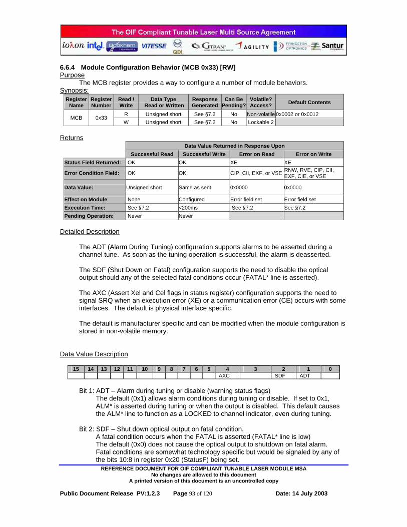
REFERENCE DOCUMENT FOR OIF COMPLIANT TUNABLE LASER MODULE MSA No changes are allowed to this document
A printed version of this document is an uncontrolled copy
Public Document Release PV:1.2.3 Page 93 of 120 Date: 14 July 2003
6.6.4 Module Configuration Behavior (MCB 0x33) [RW] Purpose
The MCB register provides a way to configure a number of module behaviors. Synopsis:
Register Name
Register Number
Read / Write
Data Type Read or Written
Response Generated
Can Be Pending?
Volatile? Access? Default Contents
R Unsigned short See §7.2 No Non-volatile 0x0002 or 0x0012 MCB 0x33
W Unsigned short See §7.2 No Lockable 2
Returns Data Value Returned in Response Upon Successful Read Successful Write Error on Read Error on Write
Status Field Returned: OK OK XE XE
Error Condition Field: OK OK CIP, CII, EXF, or VSE RNW, RVE, CIP, CII, EXF, CIE, or VSE
Data Value: Unsigned short Same as sent 0x0000 0x0000
Effect on Module None Configured Error field set Error field set Execution Time: See §7.2 <200ms See §7.2 See §7.2 Pending Operation: Never Never
Detailed Description
The ADT (Alarm During Tuning) configuration supports alarms to be asserted during a channel tune. As soon as the tuning operation is successful, the alarm is deasserted. The SDF (Shut Down on Fatal) configuration supports the need to disable the optical output should any of the selected fatal conditions occur (FATAL* line is asserted). The AXC (Assert Xel and Cel flags in status register) configuration supports the need to signal SRQ when an execution error (XE) or a communication error (CE) occurs with some interfaces. The default is physical interface specific. The default is manufacturer specific and can be modified when the module configuration is stored in non-volatile memory.
Data Value Description
15 14 13 12 11 10 9 8 7 6 5 4 3 2 1 0 AXC SDF ADT
Bit 1: ADT – Alarm during tuning or disable (warning status flags)
The default (0x1) allows alarm conditions during tuning or disable. If set to 0x1, ALM* is asserted during tuning or when the output is disabled. This default causes the ALM* line to function as a LOCKED to channel indicator, even during tuning.
Bit 2: SDF – Shut down optical output on fatal condition. A fatal condition occurs when the FATAL is asserted (FATAL* line is low) The default (0x0) does not cause the optical output to shutdown on fatal alarm. Fatal conditions are somewhat technology specific but would be signaled by any of the bits 10:8 in register 0x20 (StatusF) being set.

REFERENCE DOCUMENT FOR OIF COMPLIANT TUNABLE LASER MODULE MSA No changes are allowed to this document
A printed version of this document is an uncontrolled copy
Public Document Release PV:1.2.3 Page 94 of 120 Date: 14 July 2003
Bit 4: AXC – Assert XEL and CEL flags in the status register for the current command.
The XEL flag is always asserted when pending commands generate an execution error. In SPI mode, it may be desirable to have the XEL and CEL flags such that an SRQ* can be asserted. A “1” indicates that XEL and CEL will be asserted for the current command. A “0” indicates that XEL will only be asserted for pending commands that fail. The CEL flag will never be asserted.
Interface IOMODE State Latched At
Reset/Power Up
IOMODE1 State Latched At
Reset/Power Up
Default Value of AXC Bit
SPI LOW LOW 0x1 RS232 HIGH LOW 0x0 I2C LOW HIGH 0x1 Vendor specific HIGH HIGH 0x0
6.6.5 Grid Spacing (Grid 0x34) [RW] Purpose
Grid sets the module’s grid spacing for the channel to frequency mapping.
Synopsis: Register
Name Register Number
Read / Write
Data Type Read or Written
Response Generated
Can Be Pending?
Volatile? Access? Default Contents
R See §7.2 No Non-volatile Manufacturer specific Grid 0x34
W Signed short
(GHz*10) See §7.2 No Lockable 2
Returns Data Value Returned in Response Upon Successful Read Successful Write Error on Read Error on Write
Status Field Returned: OK OK XE XE
Error Condition Field: OK OK CIP, CII, EXF, or VSE RNW, CIP, CII, EXF, CIE, or VSE
Data Value: Signed short (GHz*10) Same as sent 0x0000 0x0000
Effect on Module None Set grid spacing – no immediate impact on frequency
Error field set Error field set
Execution Time: See §7.2 See §7.2 See §7.2 See §7.2 Pending Operation: Never Never
Detailed Description
The frequency for a channel is defined as: Freq (GHz) = (Channel –1) *grid_spacing(0x34/10) + Frequency_of_first_channel(0x35,36).
This value can only be changed when the output is disabled. Changing it while the optical output is enabled generates an execution error. This register is only used during tuning to set the output frequency register. Any grid spacing can be set but may result in many unreachable channel frequencies. The default is manufacturer specific and can be modified when the module configuration is stored in non-volatile memory.

REFERENCE DOCUMENT FOR OIF COMPLIANT TUNABLE LASER MODULE MSA No changes are allowed to this document
A printed version of this document is an uncontrolled copy
Public Document Release PV:1.2.3 Page 95 of 120 Date: 14 July 2003
Data Value Description
The register is a signed integer and allows for grid spacings as high as ±3.28 THz and as low as 0.1 GHz.
6.6.6 First Channel’s Frequency (FCF1, FCF2 0x35 – 0x36) [RW] Purpose
The FCF1 and FCF2 registers provide a way to configure the frequency of channel 1. Synopsis:
Register Name
Register Number
Read / Write
Data Type Read or Written
Response Generated
Can Be Pending?
Volatile? Access? Default Contents
R See §7.2 No Non-volatile Manufacturer specific FCF1 0x35
W Unsigned short
(THz) See §7.2 No Lockable 2 R See §7.2 No Non-volatile Manufacturer specific
FCF2 0x36 W
Unsigned short (GHz*10) See §7.2 No Lockable 2
Returns
Data Value Returned in Response Upon Successful Read Successful Write Error on Read Error on Write
Status Field Returned: OK OK XE XE
Error Condition Field: OK OK CIP, CII, EXF, or VSE RNW, CIP, CII, EXF, VSE, or CIE
Data Value: Unsigned short Same as sent 0x0000 0x0000
Effect on Module None Configured Error field set Error field set Execution Time: See §7.2 See §7.2 See §7.2 See §7.2 Pending Operation: Never Never
Detailed Description
This value can only be changed when the output is disabled. Changing it while the output is enabled will generate an execution error. The register contents are unsigned integers. The order in which LF1 and LF2 are written is not significant. Both should be defined properly before either enabling the optical output or saving the module’s configuration as the default configuration (See §6.4.9 General Module Configuration (GenCfg 0x08) [RW]).
Data Value Description The frequency is in GHz is equal to (0x35*103 + 0x36*10-1). For instance, 194.175 THz would be represented by
Register Hex Value Decimal Value 0x35 0x00C2 194 0x36 0x06D6 1750
Frequency (GHz) is then 194*103 + 1750*10-1 or 194175.0 GHz. The default value for this register will be manufacturer specific.

REFERENCE DOCUMENT FOR OIF COMPLIANT TUNABLE LASER MODULE MSA No changes are allowed to this document
A printed version of this document is an uncontrolled copy
Public Document Release PV:1.2.3 Page 96 of 120 Date: 14 July 2003
6.6.7 Laser Frequency (LF1, LF2 0x40 – 0x41) [R] Purpose
The LF1 and LF2 registers provide a way to read the frequency of the current channel. Synopsis:
Register Name
Register Number
Read / Write
Data Type Read or Written
Response Generated
Can Be Pending?
Volatile? Access? Default Contents
R Unsigned short (THz) See §7.2 No Manufacturer specific
LF1 0x40 W
R Unsigned short (GHz*10) See §7.2 No Manufacturer specific
LF2 0x41 W
Returns
Data Value Returned in Response Upon Successful Read Successful Write Error on Read Error on Write
Status Field Returned: OK XE Error Condition Field: OK CIP, CII, EXF, or VSE
Data Value: Unsigned short 0x0000
Effect on Module None Error field set Execution Time: See §7.2 See §7.2 Pending Operation: Never
Detailed Description
The frequency for a channel is computed as follows: Freq (GHz) = (Channel –1) *grid_spacing(0x34/10) + Frequency_of_first_channel(0x35,36). The laser may or not have its optical output enabled when the register is read.
Data Value Description The frequency is in GHz is equal to (0x40*103 + 0x41*10-1). Default value consistent with Grid spacing register and channel number. For instance, 194.175 THz would be represented by
Register Hex Value Decimal Value
0x40 0x00C2 194 0x41 0x06D6 1750
Frequency (GHz) is then 194*103 + 1750*10-1
REFERENCE DOCUMENT FOR OIF COMPLIANT TUNABLE LASER MODULE MSA No changes are allowed to this document
A printed version of this document is an uncontrolled copy
Public Document Release PV:1.2.3 Page 97 of 120 Date: 14 July 2003
6.6.8 Optical Output Power (OOP 0x42) [R] Purpose
The OOP register provides a way to read the external optical power estimate. Synopsis:
Register Name
Register Number
Read / Write
Data Type Read or Written
Response Generated
Can Be Pending?
Volatile? Access? Default Contents
R Signed short (dBm*100) See §7.2 No Manufacturer specific
OOP 0x42 W
Returns
Data Value Returned in Response Upon Successful Read Successful Write Error on Read Error on Write
Status Field Returned: OK XE Error Condition Field: OK CIP, CII, EXF, or VSE
Data Value: Signed short (dBm*100) 0x0000
Effect on Module None Error field set Execution Time: See §7.2 See §7.2 Pending Operation: Never
Detailed Description
The optical module’s output power. This value is in dBm*100 and is a signed integer. In units with internal power monitors, this is of course, an approximate value.
Data Value Description The optical output power is stored as a signed integer as dBm*100.
6.6.9 Current Temperature (CTemp 0x43) [R] Purpose
The CTemp register provides a way to read the current temperature of the primary control temperature.
Synopsis: Register
Name Register Number
Read / Write
Data Type Read or Written
Response Generated
Can Be Pending?
Volatile? Access? Default Contents
R Signed short (ºC*100) See §7.2 No Manufacturer specific
CTemp 0x43 W
Returns
Data Value Returned in Response Upon Successful Read Successful Write Error on Read Error on Write
Status Field Returned: OK XE Error Condition Field: OK CIP, CII, EXF, or VSE
Data Value: Signed short (ºC*100) 0x0000
Effect on Module None Error field set Execution Time: See §7.2 See §7.2 Pending Operation: Never

REFERENCE DOCUMENT FOR OIF COMPLIANT TUNABLE LASER MODULE MSA No changes are allowed to this document
A printed version of this document is an uncontrolled copy
Public Document Release PV:1.2.3 Page 98 of 120 Date: 14 July 2003
Detailed Description The current temperature reported as an integer encoded in 0.01ºC. The temperature set point is vendor specific. This register displays the temperature value used to determine if a fatal thermal condition has occurred.
Data Value Description The temperature is represented as signed short integer with units of ºC*100.
6.7 Module’s Capabilities 6.7.1 Optical Power Min/Max Set Points (OPSL, OPSH 0x50 – 0x51) [R] Purpose
The OPSL and OPSH registers provide a way to read the minimum and maximum optical power capabilities of the module.
Synopsis: Register
Name Register Number
Read / Write
Data Type Read or Written
Response Generated
Can Be Pending?
Volatile? Access? Default Contents
R Signed short (dBm*100) See §7.2 No Manufacturer specific OPSL
(Min) 0x50 W
R Signed short (dBm*100) See §7.2 No Manufacturer specific OPSH
(Max) 0x51 W
Returns
Data Value Returned in Response Upon Successful Read Successful Write Error on Read Error on Write
Status Field Returned: OK XE Error Condition Field: OK CIP, CII, EXF, or VSE
Data Value: Signed short (dBm*100) 0x0000
Effect on Module None Error field set Execution Time: See §7.2 See §7.2 Pending Operation: Never
Detailed Description
These registers report the minimum optical power setting which is possible (OPSL) and the maximum setting which is possible (OPSH) for the module.
Data Value Description The value is represented as dBm*100, signed short integer.

REFERENCE DOCUMENT FOR OIF COMPLIANT TUNABLE LASER MODULE MSA No changes are allowed to this document
A printed version of this document is an uncontrolled copy
Public Document Release PV:1.2.3 Page 99 of 120 Date: 14 July 2003
6.7.2 Laser’s First/Last Frequency (LFL1/2, LFH1/2 0x52-0x55) [R] Purpose
Returns the min and max frequency that the module supports. Synopsis:
Register Name
Register Number
Read / Write
Data Type Read or Written
Response Generated
Can Be Pending?
Volatile? Access? Default Contents
R Unsigned short (THz) See §7.2 No Manufacturer specific LFL1
(Min) 0x52 W
R Unsigned short (GHz*10) See §7.2 No Manufacturer specific LFL2
(Min) 0x53 W
R Unsigned short (THz) See §7.2 No Manufacturer specific LFH1
(Min) 0x54 W
R Unsigned short (GHz*10) See §7.2 No Manufacturer specific LFH2
(Max) 0x55 W
Returns
Data Value Returned in Response Upon Successful Read Successful Write Error on Read Error on Write
Status Field Returned: OK XE Error Condition Field: OK CIP, CII, EXF, or VSE
Data Value: Unsigned short 0x0000
Effect on Module None Error field set Execution Time: See §7.2 See §7.2 Pending Operation: Never
Detailed Description
The register set (LFL1:LFL2) returns the lowest frequency of the laser. The register set (LFH1:LFH2) returns the highest frequency of the laser.
Data Value Description The laser’s first frequency is in GHz is equal to (0x52*103 + 0x53*10-1). The laser’s last frequency is in GHz is equal to (0x54*103 + 0x55*10-1). For instance, 194.175 THz would be represented by
Register Hex Value Decimal Value
0x52, 0x54 0x00C2 194 0x53, 0x55 0x06D6 1750
Frequency (GHz) is then 194*103 + 1750*10-1

REFERENCE DOCUMENT FOR OIF COMPLIANT TUNABLE LASER MODULE MSA No changes are allowed to this document
A printed version of this document is an uncontrolled copy
Public Document Release PV:1.2.3 Page 100 of 120 Date: 14 July 2003
6.7.3 Laser’s Minimum Grid Spacing (LGrid 0x56) Purpose
The LGrid register provides a way to read the minimum grid spacing capability of the module.
Synopsis: Register
Name Register Number
Read / Write
Data Type Read or Written
Response Generated
Can Be Pending?
Volatile? Access? Default Contents
R Unsigned short (GHz*10) See §7.2 No Manufacturer specific
LGrid 0x56 W
Returns
Data Value Returned in Response Upon Successful Read Successful Write Error on Read Error on Write
Status Field Returned: OK XE Error Condition Field: OK CIP, CII, EXF, or VSE
Data Value: Unsigned short (GHz*10) 0x0000
Effect on Module None Error field set Execution Time: See §7.2 See §7.2 Pending Operation: Never
Detailed Description
The LGrid register returns the laser’s minimum grid spacing.
Data Value Description The value is represented as GHz*10.

REFERENCE DOCUMENT FOR OIF COMPLIANT TUNABLE LASER MODULE MSA No changes are allowed to this document
A printed version of this document is an uncontrolled copy
Public Document Release PV:1.2.3 Page 101 of 120 Date: 14 July 2003
6.8 MSA Commands
6.8.1 Module Currents (Currents 0x57) [R] Purpose:
Currents returns an array of the technology specific currents. These currents may include diode current(s), TEC currents, and monitor currents.
Synopsis: Register
Name Register Number
Read / Write
Data Type Read or Written
Response Generated
Can Be Pending?
Volatile? Access? Default Contents
R AEA
(Array of Unsigned Int)
See §7.2 No 0x00xx
Current Array (mA*10) Currents 0x57
W
Returns Data Value Returned in Response Upon Successful Read Successful Write Error on Read Error on Write
Status Field Returned: OK XE Error Condition Field: OK CIP, CII, EXF, or VSE
Data Value: 0x00xx
Current Array (mA*10)
0x0000
Effect on Module AEA registers configured to reference array
Error field set
Execution Time: See §7.2 See §7.2 Pending Operation: Never
Detailed Description
Returns key module currents as an array of signed integers. The first access of the Currents register returns a byte count to be read from the AEA register. At the time the Currents register is accessed, all the current values of the currents are copied into the field region where the AEA register will be configured for reading. The maximum length of the returned array 20 bytes. All devices will report the following currents:
Number of Bytes Technology 1 Technology 2
1:2 TEC TEC 3:4 Diode Diode 1 5:6 -- Diode 2 7:8 -- Diode 3
9:10 -- Diode 4 11:12 -- SOA
Data Value Description Unless otherwise specified, currents are represented as unsigned integers (mA*10).

REFERENCE DOCUMENT FOR OIF COMPLIANT TUNABLE LASER MODULE MSA No changes are allowed to this document
A printed version of this document is an uncontrolled copy
Public Document Release PV:1.2.3 Page 102 of 120 Date: 14 July 2003
6.8.2 Module Temperatures (Temps 0x58) [R] Purpose:
Temps returns an array of the technology specific temperatures. These temperatures may include diode temperatures(s), and case temperatures.
Synopsis: Register
Name Register Number
Read / Write
Data Type Read or Written
Response Generated
Can Be Pending?
Volatile? Access? Default Contents
R AEA
(Array of Unsigned Int)
See §7.2 No 0x00xx
Temperature Array (ºC*100) Temps 0x57
W
Returns Data Value Returned in Response Upon Successful Read Successful Write Error on Read Error on Write
Status Field Returned: OK XE Error Condition Field: OK CIP, CII, EXF, or VSE
Data Value: 0x00xx
Temperature Array(ºC*100)
0x0000
Effect on Module AEA registers configured to reference array
Error field set
Execution Time: See §7.2 See §7.2 Pending Operation: Never
Detailed Description
Returns key module temperatures as an array of signed integers. The first access of the Temps register returns a byte count to be read from the AEA register. At the time the Temps register is accessed, all the temperature values of the temperatures are copied into the field region where the AEA register will be configured for reading. The maximum length of the returned array 20 bytes. All devices will report the following currents:
Number of Bytes Technology 1 Technology 2
1:2 Diode Temp Diode Temp 3:4 Case Temp Case Temp
Data Value Description Unless otherwise specified, currents are represented as unsigned integers (ºC*100).

REFERENCE DOCUMENT FOR OIF COMPLIANT TUNABLE LASER MODULE MSA No changes are allowed to this document
A printed version of this document is an uncontrolled copy
Public Document Release PV:1.2.3 Page 103 of 120 Date: 14 July 2003
6.8.3 Analog & Digital Dither (Dither(E,R,A,F) 0x59-0x5C) [RW] [Optional] Purpose
The dither registers provide a way to configure dither performance of the units. Both analog and digital dither are optional features. For consistency among the various technologies, digital dither is the preferred implementation.
Synopsis: Register
Name Register Number
Read / Write
Data Type Read or Written
Response Generated
Can Be Pending?
Volatile? Access? Default Contents
R See §7.2 No Non-volatile Manufacturer specific DitherE 0x59
W Unsigned short
See §7.2 Yes Lockable 1
R See §7.2 No Non-volatile Manufacturer Specific (10KHz – 200kHz) DitherR 0x5A
W
Unsigned short (KHz)
See §7.2 Yes Lockable 2 R See §7.2 No Non-volatile Manufacturer specific
DitherF 0x5B W
Unsigned short (GHz*10) See §7.2 No Lockable 2
R See §7.2 No Non-volatile Manufacturer specific DitherA 0x5C
W Unsigned short
(%*10) See §7.2 No Lockable 2
Returns Data Value Returned in Response Upon Successful Read Successful Write Error on Read Error on Write
Status Field Returned: OK OK XE XE
Error Condition Field: OK OK CIP, CII, EXF, or VSE RNW, CIP, CII, EXF, or VSE
Data Value: Unsigned short Same as sent 0x0000 0x0000
Effect on Module None Configured Error field set Error field set Execution Time: See §7.2 See §7.2 See §7.2 See §7.2
Pending Operation: Never Technology Dependent
Detailed Description
The use of dither generally falls into two categories: 1) SBS suppression, and/or 2) signaling. SBS suppression is primarily concerned with FM frequency deviation and traditionally may monitor the AM content as a measure of the FM content. The signaling application makes use of either a sinusoidal tone or an AM modulated signal. The signaling application may also be used in conjunction with SBS suppression. Some laser technologies must generate AM content to achieve the desired FM content while other can achieve AM and FM contents independently. The configuration registers provides the ability to set the FM deviation with the DitherF register and the AM content with the DitherA register. For a given application, it is recommended that either the DitherA or the DitherF register be configured. Configuring both may lead to an over constrained system. Enabling or disabling dither is a non-interrupting traffic event. The default is manufacturer specific and can be modified when the module configuration is stored in non-volatile memory.

REFERENCE DOCUMENT FOR OIF COMPLIANT TUNABLE LASER MODULE MSA No changes are allowed to this document
A printed version of this document is an uncontrolled copy
Public Document Release PV:1.2.3 Page 104 of 120 Date: 14 July 2003
Typical Dither Configurations Register
Application DitherE DitherR DitherA DitherF
AM Tone Signaling 0x0002 (Sinusoidal) 100-200kHz Configure (~5%) Not configured
SBS Suppression (Pure) 0x0012 (Triangular) 10-50kHz50 Not configured 0.1-1GHz
AM Tone + SBS (potentially over constrained)51
0x0002 (Sinusoidal) 100-200kHz Configure (~5%) Not configured
DitherF, DitherR, and DitherA can only be changed when the digital dither is disabled. When digital dither is enabled, analog dither is disabled. Changing it while the output is enabled will generate an execution error. Values not supported by the module also generate execution errors. The contents of the registers are unsigned integers.
Data Value Description DitherR is an unsigned integer specifying the dither rate as kHz. Note that DitherE is used to set the waveform for this frequency. DitherF is an unsigned short integer encoded as the FM p-p frequency deviation as GHz*10. DitherA is an unsigned short integer encoded as the AM p-p amplitude deviation as 10*percentage of the optical power. DitherE is an unsigned short integer encoded as shown below.
15 14 13 12 11 10 9 8 7 6 5 4 3 2 1 0 WF DE (Dither Enable)
Dither Enable (Bits 1:0)
0x00 – No dither is enabled. 0x01 – Analog dither is enabled (through the Adither pin) 0x02 – Digital dither is enabled (configured through DitherF and DitherA registers) 0x03 – Invalid. Attempt to set this value triggers an execution error.
WF (Waveform) (Bits 5:4) 0x00 – Sinusoidal 0x01 – Triangular (symmetrical)
50 The granularity in setting the DitherR rate is manufacturer dependent. The module will default to the closest DitherR value supported. 51 In technologies where the SBS may be over constrained, the SBS may occur at the “pure SBS” DitherR default value and the AM tone is produced at the specified DitherR value.

REFERENCE DOCUMENT FOR OIF COMPLIANT TUNABLE LASER MODULE MSA No changes are allowed to this document
A printed version of this document is an uncontrolled copy
Public Document Release PV:1.2.3 Page 105 of 120 Date: 14 July 2003
6.8.4 TCase Warning Limits (TCaseL, TCaseH 0x5D, 0x5E) [RW] Purpose
The TCase registers set the warning limits for high and low temperature for the thermal warning.
Synopsis: Register
Name Register Number
Read / Write
Data Type Read or Written
Response Generated
Can Be Pending?
Volatile? Access? Default Contents
R See §7.2 No Non-volatile 0xFE0C (-5 ºC) TCaseL 0x5D
W Signed short
(ºC*100) See §7.2 No Lockable 2 R See §7.2 No Non-volatile 0x1B58 (+70ºC)
TCaseH 0x5E W
Signed short (ºC*100) See §7.2 No Lockable 2
Returns
Data Value Returned in Response Upon Successful Read Successful Write Error on Read Error on Write
Status Field Returned: OK OK XE XE
Error Condition Field: OK OK CIP, CII, EXF, or VSE RNW, RVE, CIP, CII, EXF, or VSE
Data Value: Signed short (ºC*100) Same as sent 0x0000 0x0000
Effect on Module None New warning levels take effect Error field set Error field set
Execution Time: See §7.2 See §7.2 See §7.2 See §7.2 Pending Operation: Never Never
Detailed Description
The temperature case limits are set by TCaseH and TCaseL. When the case temperature as determined by the laser module exceeds either of the limits for at least 5 seconds,
TCase > TCaseH TCase < TCaseL
The thermal warning flag (WTHERM) is asserted in the StatusW (0x21) register. If the ALMT, SRQT, or FatalT registers are set to trigger off of the WTHERM or WTHERML flag, the hardware line will be asserted as well. The default is manufacturer specific and can be modified when the module configuration is stored in non-volatile memory.
Data Value Description The temperature is encoded as a signed short integer as ºC*100 which allows a temperature range of ±327 ºC.

REFERENCE DOCUMENT FOR OIF COMPLIANT TUNABLE LASER MODULE MSA No changes are allowed to this document
A printed version of this document is an uncontrolled copy
Public Document Release PV:1.2.3 Page 106 of 120 Date: 14 July 2003
6.9 Manufacturer Specific (0x80-0xFE)
These registers are reserved for manufacturer specific needs.
6.9.1 User Data Storage (User1 0xFF) Purpose
Register User1 provides a data storage area for users to store and retrieve data. The data type is not specified but is treated has an arbitrary array of unsigned short ints.
Synopsis: Register
Name Register Number
Read / Write
Data Type Read or Written
Response Generated
Can Be Pending?
Volatile? Access? Default Contents
R See §7.2 No Non-volatile Empty string; length=0 User1 0xFF
W
AEA Array of unsigned int
Max 32 bytes See §7.2 Yes Lockable 1
Returns
Data Value Returned in Response Upon Successful Read Successful Write Error on Read Error on Write
Status Field Returned: OK OK XE XE
Error Condition Field: OK OK CIP, CII, EXF, or VSE RNW, CIP, CII, EXF, or VSE
Data Value: AEA Array of unsigned int Same as sent 0x0000 0x0000
Effect on Module AEA configured for read from user data area.
AEA configured for write to user data area.
Error field set Error field set
Execution Time: See §7.2 See §7.2 See §7.2 See §7.2 Pending Operation: Never Yes
Detailed Description
User data storage areas are provided for storage to application dependent data, if any. The User1 register provides a maximum storage area of 32 bytes. The default value for the USER1 field can be stored in non-volatile memory with the GenCfg:SDC operation.
Data Value Description The data is formatted, as the application requires. The module assumes the most generic format, an array of unsigned integers. Since the storage area is not formatted, it is up to the application to take care of field length boundaries such a null termination of strings.
REFERENCE DOCUMENT FOR OIF COMPLIANT TUNABLE LASER MODULE MSA No changes are allowed to this document
A printed version of this document is an uncontrolled copy
Public Document Release PV:1.2.3 Page 107 of 120 Date: 14 July 2003
7 Optical Specifications
Unless otherwise noted, all optical specifications are over life, temperature, and other environmental conditions.
7.1 Optical Characteristics
The required optical specifications for tunable lasers are very dependent upon application. The optical performance specifications are divided into a matrix of application requirements as shown in Table 7-1.
Table 7-1: Optical Specification Requirement Matrix
Application Requirement (Tuning Speed) A B C Optical Specification Matrix
SONET/SDH Protection
SONET/SDH Restoration
Provisioning & Sparing
1 Ultra Long Haul A1 B1 C1
2 Long Haul A2 B2 C2 Application
Requirement 3 Metro A3 B3 C3
.
7.1.1 Optical Parameter Definitions
For the following optical application requirements, the following terms are defined. 7.1.1.1 Spectral Linewidth
The Line width specified is the Lorentzian component. This is related to white phase noise component of the optical field. The standard 3dB width of self-homodyne measurements sets an upper limit on the Lorentzian component, but is dominated by 1/f noise and gives a pessimistic value of LW.
7.1.1.2 SMSR (Side Mode Suppression Ratio) Defined as the ratio of the average optical power in the dominant longitudinal mode to the optical power of the most significant side mode at CW, in the presence of worst-case reflections
7.1.1.3 RIN (Relative Intensity Noise) Measured from 10MHz to 10GHz.

REFERENCE DOCUMENT FOR OIF COMPLIANT TUNABLE LASER MODULE MSA No changes are allowed to this document
A printed version of this document is an uncontrolled copy
Public Document Release PV:1.2.3 Page 108 of 120 Date: 14 July 2003
7.1.2 Application Requirement 1 (Ultra Long Haul)
Table 7.1.2-1 shows the optical specifications for the CW tunable laser for Application 1.
Table 7.1.2-1: Optical Specifications (Application 1)
Item Parameter Sym Min Typ Max Unit
ν 186.200 196.575 THz 7.1.2.1 Frequency tuning range52
λ ~1525 ~1610 nm
20mW P 12.5 13.5 14.5 7.1.2.2
Fiber Output Power (Over lifetime and all operating conditions) 10mW 9.5 10.5 11.5
dBm
7.1.2.3 Output power variation across tuning range ∆P 0.5 dB
7.1.2.4 50 GHz channel spacing ∆F -2.5 +2.5 GHz
7.1.2.5
Frequency error to ITU Grid 25 GHz channel
spacing ∆F -1.25 +1.25 GHz
7.1.2.6 Side Mode Suppression Ratio SMSR 43 dB
7.1.2.7 Relative Intensity Noise RIN -145 dB/Hz
7.1.2.8 Spectral Linewidth δf 5 MHz
7.1.2.9 Optical isolation 25 dB
7.1.2.10 Source Spontaneous Emission SSE -40 dBc/nm
7.1.2.11 Polarization Extinction Ratio over tuning range PER 20 dB
7.1.2.12 Optical attenuation while tuning or while module enabled or disabled (while |∆F| > 10GHz)53
PATT1 30 dB
7.1.2.13 Optical attenuation while tuning or while module enabled or disabled (while |∆F| ≤ 10GHz)
PATT2 0 dB
52 This range represents the full C and L bands. Applications will likely require a subset of this tuning range capability. Lasers need not necessarily support the entire tuning range unless required by an application. 53 |∆F| refers to the frequency error with respect to the desired ITU grid point.

REFERENCE DOCUMENT FOR OIF COMPLIANT TUNABLE LASER MODULE MSA No changes are allowed to this document
A printed version of this document is an uncontrolled copy
Public Document Release PV:1.2.3 Page 109 of 120 Date: 14 July 2003
7.1.3 Application Requirement 2 (Long Haul) Table 7.1.3-1 shows the optical specifications for the CW tunable laser for Application 2.
Table 7.1.3-1: Optical Specifications (Application 2)
Item Parameter Sym Min Typ Max Unit
ν 186.200 196.575 THz 7.1.3.1 Frequency tuning range54
λ ~1525 ~1610 nm
20mW P 12.5 13.5 14.5 7.1.3.2
Fiber Output Power (Over lifetime and all operating conditions) 10mW 9.5 10.5 11.5
dBm
7.1.3.3 Output power variation across tuning range ∆P 0.5 dB
7.1.3.4 50 GHz channel spacing ∆F -2.5 +2.5 GHz
7.1.3.5
Frequency error to ITU Grid 25 GHz channel
spacing ∆F -1.25 +1.25 GHz
7.1.3.6 Side Mode Suppression Ratio SMSR 40 dB
7.1.3.7 Relative Intensity Noise RIN -135 dB/Hz
7.1.3.8 Spectral Linewidth δf 10 MHz
7.1.3.9 Optical isolation 25 dB
7.1.3.10 Source Spontaneous Emission SSE -40 dBc/nm
7.1.3.11 Polarization Extinction Ratio over tuning range PER 20 dB
7.1.3.12 Optical attenuation while tuning or while module enabled or disabled (while |∆F| > 10GHz) 55
PATT1 30 dB
7.1.3.13 Optical attenuation while tuning or while module enabled or disabled (while |∆F| ≤ 10GHz)
PATT2 0 dB
54 This range represents the full C and L bands. Applications will likely require a subset of this tuning range capability. Lasers need not necessarily support the entire tuning range unless required by an application. 55 |∆F| refers to the frequency error with respect to the desired ITU grid point.

REFERENCE DOCUMENT FOR OIF COMPLIANT TUNABLE LASER MODULE MSA No changes are allowed to this document
A printed version of this document is an uncontrolled copy
Public Document Release PV:1.2.3 Page 110 of 120 Date: 14 July 2003
7.1.4 Application Requirement 3 (Metro)
Table 7.1.4-1: shows the optical specifications for the CW tunable laser for Application 3.
Table 7.1.4-1: Optical Specifications (Application 3)
Item Parameter Sym Min Typ Max Unit
ν 186.200 196.575 THz 7.1.4.1 Frequency tuning range56
λ ~1525 ~1610 nm
20mW P 12.5 13.5 14.5 7.1.4.2
Fiber Output Power (Over lifetime and all operating conditions) 10mW 9.5 10.5 11.5
dBm
7.1.4.3 Output power variation across tuning range ∆P 0.5 dB
7.1.4.4
50 GHz channel spacing ∆F -2.5 +2.5 GHz
7.1.4.5
Frequency error to ITU Grid 25 GHz channel
spacing ∆F -1.25 +1.25 GHz
7.1.4.6 Side Mode Suppression Ratio SMSR 35 dB
7.1.4.7 Relative Intensity Noise RIN -130 dB/Hz
7.1.4.8 Spectral Linewidth δF 20 MHz
7.1.4.9 Optical isolation 25 dB
7.1.4.10 Source Spontaneous Emission SSE -30 dBc/nm
7.1.4.11 Polarization Extinction Ratio over tuning range PER 18 dB
7.1.4.12 Optical attenuation while tuning or while module enabled or disabled (while |∆F| > 10GHz) 57
PATT1 30 dB
7.1.4.13 Optical attenuation while tuning or while module enabled or disabled (while |∆F| ≤ 10GHz)
PATT2 0 dB
56 This range represents the full C and L bands. Applications will likely require a subset of this tuning range capability. Lasers need not necessarily support the entire tuning range unless required by an application. 57 |∆F| refers to the frequency error with respect to the desired ITU grid point.

REFERENCE DOCUMENT FOR OIF COMPLIANT TUNABLE LASER MODULE MSA No changes are allowed to this document
A printed version of this document is an uncontrolled copy
Public Document Release PV:1.2.3 Page 111 of 120 Date: 14 July 2003
7.2 Timing Specifications
Three application requirements are shown below for tunable laser tuning times.
Table 7.2-1: Timing Specifications Item Parameter Sym Min Typ Max Unit
7.2.1 Application A (SONET/SDH Protection) tT 10 ms 7.2.2 Application B (SONET/SDH Restoration) tT 1 s
7.2.3
Frequency tuning time (Frequency is within frequency accuracy / stability spec)
Application C (Sparing/Provisioning) tT 15 s
7.2.4 Application A (SONET/SDH Protection) tT 5 ms 7.2.5 Application B (SONET/SDH Restoration) tT 50 ms
7.2.6
Maximum time allowed for module to construct a response packet
Application C (Sparing/Provisioning) tT 50 ms
7.3 Module Warm Up Time
Table 7.3-1: Module Warm Up Time
Item Parameter Sym Min Typ Max Unit
7.3.1
Module warm up time. (The worst case delay, from power up or hard reset, until the module asserts ready58 (MRDY bit in the NOP (0x00) register)
TWU 30 s
58 Assuming a valid configuration of the module.

REFERENCE DOCUMENT FOR OIF COMPLIANT TUNABLE LASER MODULE MSA No changes are allowed to this document
A printed version of this document is an uncontrolled copy
Public Document Release PV:1.2.3 Page 112 of 120 Date: 14 July 2003
8 Mechanical Specifications 8.1 Module Mechanical Outline Dimensions
Figure 8.1-1 Mechanical Outline Dimensions
30 MAX
13
76.2 MAX 62.5 MIN
Module Side View
8.6
2.8
( 2.0 ) min
PIN 1 PIN 2
PIN
(For 50.8mm width) ( 4.7 )
Connector: 40 PIN 0.05” Pluggable SAMTEC P/N FTSH-120-03-F-DV-ES or equivalent. Connector to be flush with or below module housing surface within
DETAIL A
Module Bottom View
58.40
41.30
2.0 min
4.7 ( For 50.8mm width))
1
M2.5 x 0.45 – 6H , 4 DP BOTH SIDES 4 PLACES
SEE DETAIL A
50.8 MAX
6.5 +/- 3
12mm DIA MAX
25.4 +/- 6 (for 50.8mm width)
ALL DIMS IN MM X +/-0.5 X.X +/-0.25 X.XX +/-0.13 Unless tolerance otherwise noted.
Primary heat sink surface is top of module

REFERENCE DOCUMENT FOR OIF COMPLIANT TUNABLE LASER MODULE MSA No changes are allowed to this document
A printed version of this document is an uncontrolled copy
Public Document Release PV:1.2.3 Page 113 of 120 Date: 14 July 2003

REFERENCE DOCUMENT FOR OIF COMPLIANT TUNABLE LASER MODULE MSA No changes are allowed to this document
A printed version of this document is an uncontrolled copy
Public Document Release PV:1.2.3 Page 114 of 120 Date: 14 July 2003
9 Index
A
Absolute Maximum Ratings......................................................................................................................... 24 ADT.........................................................................................................................................................87, 93 AEA.............................................................................................................................................................. 14 Alarm line..................................................................................................................................................... 29 ALM*......................................................................................................16, 17, 22, 29, 34, 78, 79, 86, 87, 93 Application space
Distance.................................................................................................................................................. 107 Long Haul............................................................................................................................................... 109 Metro ...................................................................................................................................................... 110 Tuning Time Specification ..................................................................................................................... 111 Ultra Long Haul...................................................................................................................................... 108
AXC ........................................................................................................................................................93, 94
B
BIP-4 ................................................................................................................................... 43. See Checksum Bit Numbering........................................................................................................................See Conventions boot up.......................................................................................................................................................... 25
C
CE................................................................. 16, 28, 30, 33, 43, 45, 68, 78, 80, 93. See Communication error CEL .............................................................................................................................................78, 80, 84, 94 Checksum ..................................................................................................................................................... 43 Checksum (BIP-4) ........................................................................................................................................ 11 CIE ........................................................................................................................................... See Error Field CII............................................................................................................................................. See Error Field CIP............................................................................................................................................ See Error Field Command Format......................................................................................................................................... 47 Command Group
Generic module commands ...................................................................................................................... 54 Manufacturer Specific ............................................................................................................................ 106 Optical Settings ........................................................................................................................................ 88 Status Commands ..................................................................................................................................... 77
Command Paradigms.................................................................................................................................... 12 Command volatile attribute .......................................................................................................................... 52 Commands
Command Description Format ................................................................................................................. 52 Data value................................................................................................................................................. 53 Error Condition Field ............................................................................................................................... 53 Execution Time ........................................................................................................................................ 53 Pending Operation .................................................................................................................................... 53

REFERENCE DOCUMENT FOR OIF COMPLIANT TUNABLE LASER MODULE MSA No changes are allowed to this document
A printed version of this document is an uncontrolled copy
Public Document Release PV:1.2.3 Page 115 of 120 Date: 14 July 2003
Response generated attribute .................................................................................................................... 52 Returns attribute ....................................................................................................................................... 53 Status Field Returned ............................................................................................................................... 53
Commands access attribute .......................................................................................................................... 53 Commands Can be pending.......................................................................................................................... 52 Commands:................................................................................................................................................... 53 Communication Byte Numbering................................................................................................................. 26 Communication error.................................................................................................................................... 11
RS-232...................................................................................................................................................... 28 Communication Interface .............................................................................................. See Physical Interface Connector
Electrical................................................................................................................................................... 18 Pin assignments ........................................................................................................................................ 18
Conventions.................................................................................................................................................... 6 Bit Numbering............................................................................................................................................ 6 Byte numbering ........................................................................................................................................ 26 Data Direction ............................................................................................................................................ 6 Data Types.................................................................................................................................................. 6 Numeric Values .......................................................................................................................................... 6
CRC.............................................................................See CRC-16. See CRC-16. See CRC-16. See CRC-16 CRC-16......................................................................................................................................................... 44 CRL ...................................................................................................................................................78, 80, 84
D
Data Direction ........................................................................................................................See Conventions Data Types........................................................................................................................14. See Conventions Design
Communications Interface........................................................................................................................ 10 Configurable............................................................................................................................................. 10 Extensible Platform .................................................................................................................................. 10
Document Background ................................................................................................................................................ 8 Design Objectives..................................................................................................................................... 10 List of Contributors to the OIF-IA ............................................................................................................. 9 Objectives................................................................................................................................................... 8 Scope .......................................................................................................................................................... 8
E
EAM........................................................................................................................................................66, 67 Electrical Characteristics ..........................................................................................18, 24. See Specifications ERE .......................................................................................................................................... See Error Field ERO.......................................................................................................................................... See Error Field Error Condition Field ................................................................................................................................... 53 Error Detection
By Host..................................................................................................................................................... 16 By Module................................................................................................................................................ 16
Error field ................................................................................................................................................53, 55 Error Field .................................................................................................................................................... 15

REFERENCE DOCUMENT FOR OIF COMPLIANT TUNABLE LASER MODULE MSA No changes are allowed to this document
A printed version of this document is an uncontrolled copy
Public Document Release PV:1.2.3 Page 116 of 120 Date: 14 July 2003
CIE - Command ignored while output enabled ........................................................................................ 15 CII - Command ignored while initializing................................................................................................ 15 CIP - Command ignored due to pending operation .................................................................................. 15 ERE - Extended address range error......................................................................................................... 15 ERO - Extended address is read only ....................................................................................................... 15 EXF - Execution general failure............................................................................................................... 15 IVC........................................................................................................................................................... 15 OK – No errors ......................................................................................................................................... 15 RNI – Register no implemented ............................................................................................................... 15 RNW – Register not write-able ................................................................................................................ 15 RVE – Register value range error............................................................................................................. 15 VSE - Vendor specific error ..................................................................................................................... 15
Example CRC-16..................................................................................................................................................... 45 Extended Addressing................................................................................................................................ 14 Packet Pacing ........................................................................................................................................... 46 Reading Module Status............................................................................................................................. 12
Execution Error Detection............................................................................................................................ 16 Execution Error Timing
RS-232...................................................................................................................................................... 28 EXF .......................................................................................................................................... See Error Field Extended Addressing.................................................................................................................................... 13
F
FATAL* ....................................................................................................................16, 50, 78, 79, 85, 86, 93 FFREQ ........................................................................................................................................77, 78, 79, 87 FFREQL ................................................................................................................................77, 78, 80, 84, 86 flag
CP............................................................................................................................................................. 65 FPWR....................................................................................................................................77, 78, 80, 87, 90 FPWRL..................................................................................................................................77, 78, 80, 84, 86 FTHERM.....................................................................................................................................77, 78, 80, 87 FTHERML ............................................................................................................................77, 78, 80, 84, 86 FVSF ...........................................................................................................................................77, 78, 79, 87 FVSFL...................................................................................................................................77, 78, 80, 84, 86
I
I2C Acknowledge............................................................................................................................................ 39 Bus Timing ............................................................................................................................................... 37 Complete Data Transfer ........................................................................................................................... 39 Data Transfer Timing ............................................................................................................................... 38 I2C-Bus ..................................................................................................................................................... 37 Pins Description ....................................................................................................................................... 40 Start/Stop Timing ..................................................................................................................................... 37
In-Bound packet ......................................................................................................................................43, 47 INCR .......................................................................................................................................................66, 67 Interfaces

REFERENCE DOCUMENT FOR OIF COMPLIANT TUNABLE LASER MODULE MSA No changes are allowed to this document
A printed version of this document is an uncontrolled copy
Public Document Release PV:1.2.3 Page 117 of 120 Date: 14 July 2003
Communication ........................................................................................................................................ 25 Invalid configuration, MRDY ...................................................................................................................... 55 IOCap ......................................................................................................................................................49, 63 IOCLK.......................................................................................................................................................... 31 IOMode ........................................................................................................................................................ 25 IOMode1 ...................................................................................................................................................... 25 IRDY* ...............................................................................................20, 27, 32, 33, 38, 40, 41, 45, 46, 79, 92
L
Locked line ................................................................................................................................................... 17 Locked status................................................................................................................................................ 54 Lockout Levels ............................................................................................................................................. 76 Lockout levels, register ................................................................................................................................ 15 Lockout, register................................................................................................................................16, 53, 75 Long haul.................................................................................................................................................... 107
M
Mechanical Specifications Module ................................................................................................................................................... 112
Metro .......................................................................................................................................................... 107 MRDY.........................................................................................................................................................See MRL ............................................................................................................................................78, 80, 84, 86 MS* ...............................................................................................................15, 22, 27, 28, 29, 31, 32, 40, 92 multi-byte response ...................................................................................................................................... 10
N
Numeric Values......................................................................................................................See Conventions
O
OK ............................................................................................................................................ See Error Field Optical Characteristics................................................................................................................................ 107 Out-Bound packet....................................................................................................................................43, 47 Overview
Address registers ...................................................................................................................................... 13 Command ................................................................................................................................................. 12 Command Execution Overlap .................................................................................................................. 13 Communication ........................................................................................................................................ 11 Communication Layers ............................................................................................................................ 11 Data Types................................................................................................................................................ 14
Multi-byte............................................................................................................................................. 15 Two Byte .............................................................................................................................................. 14
Error Detection ......................................................................................................................................... 16 Extended Addressing................................................................................................................................ 13 Lockout levels .......................................................................................................................................... 15 Module Reset............................................................................................................................................ 15

REFERENCE DOCUMENT FOR OIF COMPLIANT TUNABLE LASER MODULE MSA No changes are allowed to this document
A printed version of this document is an uncontrolled copy
Public Document Release PV:1.2.3 Page 118 of 120 Date: 14 July 2003
Physical Interface ..................................................................................................................................... 12 Register configuration .............................................................................................................................. 13 Register Lockout ...................................................................................................................................... 15 Transport Layer ........................................................................................................................................ 43
P
Packet Pacing ............................................................................................................................................... 45 Packet status flags
AEA.......................................................................................................................................................... 48 CP............................................................................................................................................................. 48 XE............................................................................................................................................................. 48
Packet status flags XE............................................................................................................................................................. 48
Packet Status Flags ....................................................................................................................................... 48 Pending operation......................................................................................................................................... 53 Pending operations ....................................................................................................................................... 13 Physical Interface
Selection ................................................................................................................................................... 25 Physical interfaces ........................................................................................................................................ 18
I2C............................................................................................................................................................. 36 Performance.............................................................................................................................................. 25 Pin Functions............................................................................................................................................ 20 RS-232...................................................................................................................................................... 27 SPI ............................................................................................................................................................ 31
Physical Interfaces........................................................................................................................................ 12 Pin Assignments ........................................................................................................................................... 19 Pin Functions................................................................................................................................................ 20
R
RAI............................................................................................................................................................... 66 References ...................................................................................................................................................... 6 Register
ALMT....................................................................................................................................................... 86 Channel..................................................................................................................................................... 88 CTemp...................................................................................................................................................... 97 Currents .................................................................................................................................................. 101 DevTyp..................................................................................................................................................... 55 Dither(E,R,A,F) ...................................................................................................................................... 103 DLConfig.................................................................................................................................................. 71 DLStatus................................................................................................................................................... 74 Extended Addressing................................................................................................................................ 65 FatalT ....................................................................................................................................................... 85 FCF1......................................................................................................................................................... 95 FCF2......................................................................................................................................................... 95 FFreqTh.................................................................................................................................................... 82 FPowTh .................................................................................................................................................... 81 FThermTh................................................................................................................................................. 83 GenCfg ....................................................................................................................................17, 52, 62, 95

REFERENCE DOCUMENT FOR OIF COMPLIANT TUNABLE LASER MODULE MSA No changes are allowed to this document
A printed version of this document is an uncontrolled copy
Public Document Release PV:1.2.3 Page 119 of 120 Date: 14 July 2003
Grid........................................................................................................................................................... 94 IOCap ................................................................................................................................29, 30, 34, 41, 63 LF1 ........................................................................................................................................................... 96 LF2 ........................................................................................................................................................... 96 LGrid ...................................................................................................................................................... 100 Lock...............................................................................................................................................16, 53, 75 Lockout levels .......................................................................................................................................... 15 LstResp..................................................................................................................................................... 70 MCB......................................................................................................................................................... 93 MFGDate.................................................................................................................................................. 58 MFGR....................................................................................................................................................... 56 Model ....................................................................................................................................................... 57 NOP/Status ............................................................................................................................................... 54 OOP.......................................................................................................................................................... 97 OPSH........................................................................................................................................................ 98 OPSL ........................................................................................................................................................ 98 PWR ......................................................................................................................................................... 90 RCRC ....................................................................................................................................................... 69 RelBack .................................................................................................................................................... 61 Release ..................................................................................................................................................... 59 SerNo........................................................................................................................................................ 58 SRQT........................................................................................................................................................ 84 StatusF...................................................................................................................................................... 77 StatusW .................................................................................................................................................... 77 TCaseH................................................................................................................................................... 105 TCaseL ................................................................................................................................................... 105 Temps ..................................................................................................................................................... 102 User1 Data Storage................................................................................................................................. 106 WCRC ...................................................................................................................................................... 68 WFreqTh .................................................................................................................................................. 82 WPowTh................................................................................................................................................... 81 WThermTh ............................................................................................................................................... 83
Registers Summary .................................................................................................................................................. 49
Reset, module ............................................................................................................................................... 15 Response flag ............................................................................................................................................... 11 Response generated ...................................................................................................................................... 52 RNI ........................................................................................................................................... See Error Field RNW......................................................................................................................................... See Error Field RS-232
Alarm Timing ........................................................................................................................................... 29 ASCII ....................................................................................................................................................... 29 Baud rates ................................................................................................................................................. 29 Error Timing............................................................................................................................................. 28 Execution Timing ................................................................................................................................27, 28
RVE.......................................................................................................................................... See Error Field
S
SBS suppression ......................................................................................................................................... 103 SDC - Store default configuration ................................................................................................................ 62

REFERENCE DOCUMENT FOR OIF COMPLIANT TUNABLE LASER MODULE MSA No changes are allowed to this document
A printed version of this document is an uncontrolled copy
Public Document Release PV:1.2.3 Page 120 of 120 Date: 14 July 2003
SDF..............................................................................................................................................77, 88, 92, 93 SENA ..........................................................................................................................................79, 88, 92, 93 Serial Peripheral Interface ............................................................................................................................ 31 SPI
Error Timing............................................................................................................................................. 33 Execution Timing ..................................................................................................................................... 31 Pin Timing................................................................................................................................................ 35 Pins Description ....................................................................................................................................... 31 Read/Write Timing................................................................................................................................... 33 Transfer Timing........................................................................................................................................ 35
SRQ* ..................................................................................... 16, 17, 21, 28, 33, 34, 50, 78, 79, 84, 85, 90, 94 Status Flags.................................................................................................................. See Packet Status Flags
T
Transport Layer Transport Layer Field Definitions ............................................................................................................ 43
U
Ultra long haul............................................................................................................................................ 107
V
VSE .......................................................................................................................................... See Error Field
W
WAI.............................................................................................................................................................. 66 WFREQ.......................................................................................................................................77, 78, 79, 87 WFREQL ..............................................................................................................................77, 78, 80, 84, 86 WPWR ..................................................................................................................................77, 78, 80, 87, 90 WPWRL ................................................................................................................................77, 78, 80, 84, 86 WTHERM ...........................................................................................................................77, 78, 80, 87, 105 WTHERML...................................................................................................................77, 78, 80, 84, 86, 105 WVSF..........................................................................................................................................77, 78, 79, 87 WVSFL .................................................................................................................................77, 78, 80, 84, 86
X
XE14, 16, 28, 30, 33, 54, 56, 57, 58, 59, 61, 62, 63, 65, 68, 69, 70, 71, 74, 75, 77, 78, 80, 81, 82, 83, 84, 85, 86, 88, 90, 91, 93, 94, 95, 96, 97, 98, 99, 100, 101, 102, 103, 105, 106 IVC....................................................................................................................................... See Error Field
XEL .............................................................................................................................................78, 80, 84, 94