Implementation Agreement for 100G Long-Haul DWDM ... · 9/20/2011 · OIF-MSA-100GLH-EM-01.1...
44
OIF-MSA-100GLH-EM-01.1 Implementation Agreement for 100G Long-Haul DWDM Transmission Module – Electromechanical (MSA-100GLH) IA # OIF-MSA-100GLH-EM-01.1 Date Approved September 20, 2011 Implementation Agreement created and approved by the Optical Internetworking Forum www.oiforum.com
Transcript of Implementation Agreement for 100G Long-Haul DWDM ... · 9/20/2011 · OIF-MSA-100GLH-EM-01.1...

OIF-MSA-100GLH-EM-01.1
Implementation Agreement
for 100G Long-Haul DWDM Transmission
Module – Electromechanical (MSA-100GLH)
IA # OIF-MSA-100GLH-EM-01.1
Date Approved
September 20, 2011
Implementation Agreement created and approved by the Optical Internetworking Forum
www.oiforum.com
OIF-MSA-100GLH-EM-01.1
www.oiforum.com 2
Working Group: Physical and Link Layer (PLL) Working Group TITLE: Implementation Agreement for 100G Long-Haul DWDM Transmission Module
– Electromechanical (MSA-100GLH) SOURCE: TECHNICAL EDITOR WORKING GROUP CHAIR
Jon Anderson, Ph. D. David R. Stauffer, Ph. D. Opnext, Inc. IBM Corporation 46429 Landing Parkway 1000 River Road, MC 862J Fremont, CA 94538 Essex Jct., VT 05452
Phone: +1-510-580-8832 Phone: +1-802-769-6914 Email: [email protected] Email: [email protected]
WORKING GROUP VICE CHAIR
Karl Gass Sandia National Laboratories P. O. Box 5800 MS-0874 Phone: +1-505-844-8849 Email: [email protected]
ABSTRACT: This Implementation Agreement specifies key electromechanical aspects of a 100G Long-Haul DWDM Transmission Module, for applications such as 100G PM-QPSK long-haul DWDM transmission. Key aspects include: module mechanical dimensions, electrical connector and pin assignment, module hardware signaling pins, high-speed electrical characteristics, power supply, power dissipation, and management interface.

OIF-MSA-100GLH-EM-01.1
www.oiforum.com 3
The OIF is an international non profit organization with over 90 member companies, including the world’s leading carriers and vendors. Being an industry group uniting representatives of the data and optical worlds, OIF’s purpose is to accelerate the deployment of interoperable, cost-effective and robust optical internetworks and their associated technologies. Optical internetworks are data networks composed of routers and data switches interconnected by optical networking elements.
With the goal of promoting worldwide compatibility of optical internetworking products, the OIF actively supports and extends the work of national and international standards bodies. Working relationships or formal liaisons have been established with IEEE 802.1, IEEE 802.3, IETF, IP-MPLS Forum, IPv6 Forum, ITU-T SG13, ITU-T SG15, MEF, ATIS-OPTXS, ATIS-TMOC, TMF and the CFP MSA Group.
For additional information contact: The Optical Internetworking Forum, 48377 Fremont Blvd.,
Suite 117, Fremont, CA 94538 510-492-4040 Φ [email protected]
www.oiforum.com
Notice: This Technical Document has been created by the Optical Internetworking Forum (OIF). This document is offered to the OIF Membership solely as a basis for agreement and is not a binding proposal on the companies listed as resources above. The OIF reserves the rights to at any time to add, amend, or withdraw statements contained herein. Nothing in this document is in any way binding on the OIF or any of its members.
The user's attention is called to the possibility that implementation of the OIF implementation agreement contained herein may require the use of inventions covered by the patent rights held by third parties. By publication of this OIF implementation agreement, the OIF makes no representation or warranty whatsoever, whether expressed or implied, that implementation of the specification will not infringe any third party rights, nor does the OIF make any representation or warranty whatsoever, whether expressed or implied, with respect to any claim that has been or may be asserted by any third party, the validity of any patent rights related to any such claim, or the extent to which a license to use any such rights may or may not be available or the terms hereof.
© 2011 Optical Internetworking Forum
This document and translations of it may be copied and furnished to others, and derivative works that comment on or otherwise explain it or assist in its implementation may be prepared, copied, published and distributed, in whole or in part, without restriction other than the following, (1) the above copyright notice and this paragraph must be included on all such copies and derivative works, and (2) this document itself may not be modified in any way, such as by removing the copyright notice or references to the OIF, except as needed for the purpose of developing OIF Implementation Agreements. By downloading, copying, or using this document in any manner, the user consents to the terms and conditions of this notice. Unless the terms and conditions of this notice are breached by the user, the limited permissions granted above are perpetual and will not be revoked by the OIF or its successors or assigns.
This document and the information contained herein is provided on an “AS IS” basis and THE OIF DISCLAIMS ALL WARRANTIES, EXPRESS OR IMPLIED, INCLUDING BUT NOT LIMITED TO ANY WARRANTY THAT THE USE OF THE INFORMATION HEREIN WILL NOT INFRINGE ANY RIGHTS OR ANY IMPLIED WARRANTIES OF MERCHANTABILITY, TITLE OR FITNESS FOR A PARTICULAR PURPOSE.
OIF-MSA-100GLH-EM-01.1
www.oiforum.com 4
1 Table of Contents
1 Table of Contents ....................................................................................... 4 2 List of Figures ............................................................................................ 5 3 List of Tables .............................................................................................. 5 4 Document Revision History ...................................................................... 6 5 Introduction ............................................................................................... 7 6 Functional Description .............................................................................. 7 7 Module Management Interface Description ............................................. 8 8 Electrical Specifications ............................................................................. 8
8.1 Operating Case Temperature .............................................................. 8 8.2 Electrical Power Supply and Power Dissipation ................................ 8 8.3 High Speed Pin Electrical Specifications ............................................ 9 8.4 Control Pins (non-MDIO) Functional Description ........................... 11 8.5 Alarm Pins (non-MDIO) Functional Description ............................. 14 8.6 Module Management Interface Pins (MDIO) Description .............. 17 8.7 Hardware Signaling Pin Electrical Specifications ............................ 19 8.8 Hardware Signaling Pin Timing Specifications ............................... 21
9 Mechanical Specifications ....................................................................... 23 9.1 Mechanical Overview........................................................................ 23 9.2 Electrical Connector .......................................................................... 23 9.3 Module Dimensions .......................................................................... 26 9.4 Host System Dimensions .................................................................. 31 9.5 Module Optical Fiber Ports ............................................................... 32 9.6 Pin Assignment ................................................................................. 32
10 References ............................................................................................. 36 10.1 Normative references ..................................................................... 36 10.2 Informative references ................................................................... 36
11 Appendix A: Glossary .......................................................................... 36 12 Appendix B: Open Issues / current work items ................................... 37 13 Appendix C: List of companies belonging to OIF when document is approved ......................................................................................................... 38 14 Appendix D (informative): Pin Map Allocation for 40G Applications40 15 Appendix E (informative): Optional Pin Map Allocation for 100G Applications ................................................................................................... 43

OIF-MSA-100GLH-EM-01.1
www.oiforum.com 5
2 List of Figures FIGURE 1: 100G LONG-HAUL DWDM TRANSMISSION MODULE (MSA-100GLH) FUNCTIONAL
DIAGRAM ................................................................................................................................ 8 FIGURE 2: HIGH SPEED I/O FOR DATA AND CLOCKS .................................................................... 10 FIGURE 3: TRANSMITTER DISABLE (TX_DIS) TIMING DIAGRAM ................................................ 13 FIGURE 4: MODULE LOW POWER (MOD_LOPWR) TIMING DIAGRAM ....................................... 14 FIGURE 5: RECEIVER LOSS OF SIGNAL (RX_LOS) TIMING DIAGRAM .......................................... 16 FIGURE 6: GLOBAL ALARM (GLB_ALRMN) TIMING DIAGRAM .................................................. 17 FIGURE 7: MODULE MDIO & MDC TIMING DIAGRAM ................................................................ 19 FIGURE 8: REFERENCE +3.3V LVCMOS INPUT/OUTPUT TERMINATIONS .................................... 20 FIGURE 9: REFERENCE MDIO INTERFACE TERMINATION ............................................................ 21 FIGURE 10: MSA-100GLH SIMPLIFIED START-UP FLOW DIAGRAM ............................................ 22 FIGURE 11: HIROSE FX10A-168S-SV(83) RECEPTACLE CONNECTOR ASSEMBLY ...................... 24 FIGURE 12: HIROSE FX10A-168P-SV(83) HEADER CONNECTOR ASSEMBLY .............................. 25 FIGURE 13: FX10 CONNECTOR ALIGNMENT ................................................................................. 26 FIGURE 14: MSA-100GLH NON-CONDUCTIVE SHEET DIMENSIONS ............................................ 27 FIGURE 15: MSA-100GLH FLATTOP MECHANICAL DIMENSIONS - BOTTOM/SIDE VIEWS ............. 28 FIGURE 16: MSA-100GLH FLATTOP MECHANICAL DIMENSIONS - TOP VIEW .............................. 29 FIGURE 17: MECHANICAL DIMENSIONS OF MSA-100GLH WITH INTEGRATED HEAT SINK ........ 30 FIGURE 18: MSA-100GLH WITH INTEGRATED HEAT SINK - TOP VIEW ....................................... 31 FIGURE 19: RECOMMENDED HOST SYSTEM LAYOUT FOR MSA-100GLH ................................... 31 FIGURE 20: MSA-100GLH OPTICAL FIBER PORT LOCATION AND DIMENSIONS ......................... 32
3 List of Tables TABLE 1: MSA-100GLH PERFORMANCE SPECIFICATIONS ............................................................. 9 TABLE 2: MSA-100GLH REFERENCE CLOCK (REFCLK) CHARACTERISTICS ............................. 10 TABLE 3: OPTIONAL TXMCLK AND RXMCLK CHARACTERISTICS ............................................ 11 TABLE 4: MSA-100GLH CONTROL PINS (NON-MDIO) ................................................................ 12 TABLE 5: MSA-100GLH ALARM PINS (NON-MDIO) ................................................................... 15 TABLE 6: MSA-100GLH MDIO MANAGEMENT INTERFACE PINS ............................................... 18 TABLE 7: 3.3V LVCMOS ELECTRICAL CHARACTERISTICS .......................................................... 19 TABLE 8: 1.2V LVCMOS ELECTRICAL CHARACTERISTICS .......................................................... 20 TABLE 9: HARDWARE SIGNALING PINS TIMING PARAMETERS SUMMARY ................................... 22 TABLE 10: MSA-100GLH PIN-MAP .............................................................................................. 33 TABLE 11: MSA-100GLH ELECTRICAL CONNECTOR - ROW B PIN DESCRIPTION ....................... 34 TABLE 12: MSA-100GLH ELECTRICAL CONNECTOR - ROW A PIN DESCRIPTION ....................... 35 TABLE 13: MSA-100GLH ELECTRICAL CONNECTOR - ROW B PIN MAP (40G APPLICATION) .... 41 TABLE 14: MSA-100GLH ELECTRICAL CONNECTOR - ROW A PIN MAP (40G APPLICATION) .... 42 TABLE 15: MSA-100GLH ELECTRICAL CONNECTOR - ROW A PIN DESCRIPTION OPTION .......... 44

OIF-MSA-100GLH-EM-01.1
www.oiforum.com 6
4 Document Revision History Working Group: Physical and Link Layer (PLL) Working Group SOURCE: TECHNICAL EDITOR WORKING GROUP CHAIR
Jon Anderson, Ph. D. David R. Stauffer, Ph. D. Opnext, Inc. IBM Corporation 46429 Landing Parkway 1000 River Road, MC 862J Fremont, CA 94538 Essex Jct., VT 05452
Phone: +1-510-580-8832 Phone: +1-802-769-6914 Email: [email protected] Email: [email protected]
WORKING GROUP VICE CHAIR
Karl Gass Sandia National Laboratories P. O. Box 5800 MS-0874 Phone: +1-505-844-8849 Email: [email protected]
DATE: September 20, 2011 Revision Date Change Notes By OIF-MSA-100GLH-EM-01.0 June 8, 2010 Initial Release J. Anderson OIF-MSA-100GLH-EM-01.1 Sept. 20,
2011 Maintenance Release: - Added Appendix E (informative); - Clarification on module optical fiber boot exit area keep-out (Sec. 9.5) - Clarification on host-module connector mating condition (Sec. 9.3) - Clarification on mounting hole dimensions in Figures 15-17 - Modified Reference MDIO Interface Termination (Figure 9) - Minimum pulse widths specified for MDC and PM_SYNC pins in Table 9. - Added Informative Reference to CFP MSA Management Interface Specification V2.0
J. Anderson
OIF-MSA-100GLH-EM-01.1
www.oiforum.com 7
5 Introduction This document details an Implementation Agreement (IA) for a 100G Long-Haul DWDM Transmission Module – Electromechanical (MSA-100GLH) for optical line interface applications. While specifically addressing 100G PM-QPSK long-haul DWDM transmission applications [I1], this IA strives to remain modulation format and data rate agnostic whenever practical to maximize applicability to future market requirements. This IA specifies key electromechanical aspects of the 100G Long-Haul DWDM Transmission Module (hereafter termed MSA-100GLH) that include the following: module mechanical dimensions, electrical connector and pin map, module hardware signaling pins, high-speed electrical characteristics, power supply, power dissipation, and management interface. 6 Functional Description A functional block diagram of the MSA-100GLH is illustrated in Figure 1: 100G Long-Haul DWDM Transmission Module (MSA-100GLH) Functional Diagram Key module functions include transmitter optics, receiver optics, interface ICs, module controller supporting an MDIO/MDC management interface, and power conversion for a single +12V DC power supply from the host. The MSA-100GLH is not hot pluggable, but is fastened to the host system board during line card assembly. The interface IC(s) and module electrical interface are generically specified to allow vendor specific customization of multilane “M-lane” ~ 11 Gbit/s interfaces. Module electrical interfaces include but are not limited to the following:
a) Simple bit multiplex b) OTL4.10 [I2] c) SFI-S [I3] d) OTL3.4 [I2] (for 40G applications, see informative Appendix D)

OIF-MSA-100GLH-EM-01.1
www.oiforum.com 8
Figure 1: 100G Long-Haul DWDM Transmission Module (MSA-100GLH) Functional Diagram
7 Module Management Interface Description The MSA-100GLH utilizes MDIO IEEE 802.3 Clause 45 [N1] for its management interface. The MSA-100GLH MDIO hardware implementation is specified in Section 8.6. The MSA-100GLH MDIO register set specifications are defined in [I5]. When multiple MSA-100GLH are connected via a single bus, a particular MSA-100GLH may be selected by using the MDIO Physical Port Address pins. 8 Electrical Specifications 8.1 Operating Case Temperature The MSA-100GLH operating case temperature is specified in Table 1. 8.2 Electrical Power Supply and Power Dissipation The MSA-100GLH is powered by a single +12V DC supply from the host board. This power supply is specified in Table 1. All voltages are measured at the electrical connector interface. The MSA-100GLH power dissipation is specified in Table 1.

OIF-MSA-100GLH-EM-01.1
www.oiforum.com 9
Table 1: MSA-100GLH Performance Specifications
Parameter Symbol Min Typ Max Unit Note +12V DC Supply Voltage VCC 11.4 12.0 12.6 V +/- 5% +12V DC Supply Current ICC 8.0 A Notes 1 & 2 Power Supply Noise Vrip 1
%p-p 1Hz – 20MHz
Power Dissipation Pw 80 W Operating Case Temperature 0 70 °C
Note: The parameter min and max values are specified End-of-Life within the overall relevant operating case temperature range. The typical values are referenced to +25°C, nominal power supply, Beginning-of -Life. Note 1: Maximum current per pin shall not exceed 750mA. Note 2: Icc max specified for current rating purposes. Normal operating current (Icc) must not exceed Pw / Vcc. 8.3 High Speed Pin Electrical Specifications 8.3.1 Transmitter Data (TX) The Transmitter Data (TX) signals shall comply with CEI-11G-MR Low Swing option as per Clauses 9.3.1. and 9.3.1.2 [N2]. Full Swing support is not required. The recommended termination of the TX pins is given in Figure 2. 8.3.2 Receiver Data (RX) The Receiver Data (RX) signals shall comply with CEI-11G-MR Clause 9.3.3 [N2]. The recommended termination of the RX pins is given in Figure 2. 8.3.3 Reference Clock (REFCLK) The host shall supply a reference clock (REFCLK) at 1/16 of the electrical lane rate. The host shall optionally supply a reference clock (REFCLK) at 1/64 of the electrical lane rate. The REFCLK shall be CML differential AC coupled and terminated with 50 Ohm internal VTT within the MSA-100GLH, as shown in Figure 2. A frequency locked relationship is required between the transmit data lanes (TX/TXDSC) and the reference clock (REFCLK). There is no required phase relationship between the data lanes and the reference clock. The REFCLK frequency shall not deviate from nominal by more than ±20 ppm. Detailed reference clock characteristics for the MSA-100GLH are given in Table 2.

OIF-MSA-100GLH-EM-01.1
www.oiforum.com 10
Table 2: MSA-100GLH Reference Clock (REFCLK) Characteristics
Parameter Symbol Min Typ Max Unit Notes Impedance Zd 80 100 120 Ω Frequency f 1/16 Of electrical lane rate -
default 1/64 Of electrical lane rate -
optional Frequency Stability
Δf -20 +20 ppm
Differential Voltage
VDIFF 400 1600 mV Peak-to-Peak Differential
Clock Duty Cycle CDC 40 60 % Clock Rise/Fall Time
tr/f 200 1250 ps 1/64 electrical lane rate 50 315 ps 1/16 electrical lane rate
Figure 2: High Speed I/O for Data and Clocks
8.3.4 Transmitter Monitor Clock (TXMCLK) The MSA-100GLH optionally may supply a transmitter monitor clock (TXMCLK). This clock is intended to be used as a reference for measurements of the module optical transmit signal. If provided, the clock shall operate at 1/8 of the transmitter optical symbol rate for 32Gb
OIF-MSA-100GLH-EM-01.1
www.oiforum.com 11
applications1. This rate is optimized for triggering high-speed sampling scopes. Clock termination is shown in Figure 2. TXMCLK characteristics are summarized in Table 3. 8.3.5 Receiver Monitor Clock (RXMCLK) The MSA-100GLH optionally may supply a receiver monitor clock (RXMCLK). This clock is intended to be used as a reference for measurements of the module receive data. If provided, the clock shall operate at 1/16 of the receiver electrical lane data rate. The RXMCLK may optionally operate at 1/64 of the receiver electrical lane data rate. Clock termination is shown in Figure 2. RXMCLK characteristics are summarized in Table 3.
Table 3: Optional TXMCLK and RXMCLK Characteristics
Parameter Symbol Min Typ Max Unit Notes Impedance Zd 80 100 120 Ω Frequency - TXMCLK
1/8 Of TX optical symbol rate - default
Frequency - RXMCLK
1/16 Of RX electrical lane data rate - default
1/64 Of RX electrical lane data rate - optional
Output Differential Voltage
VDIFF 400 1600 mV Peak-to-Peak Differential
Clock Duty Cycle CDC 40 60 % 8.4 Control Pins (non-MDIO) Functional Description The control functions between a host and a MSA-100GLH are conducted through a set of dedicated, non-data hardware signal pins on the 168-pin electrical connector and via an MDIO interface. The signal pins work together with the MDIO interface to form a complete HOST/MSA-100GLH management interface. Upon module initialization, the control functions are available. Pins allocated to control functions in the 168-pin electrical connector are listed in Table 4.
1 For 40G applications, other clock rates may be necessary for operating with available test equipment.

OIF-MSA-100GLH-EM-01.1
www.oiforum.com 12
Table 4: MSA-100GLH Control Pins (non-MDIO)
Pin #
Symbol Description I/O
Logic “H” “L” Pull-up /down
B20 PRG_CNTL1 Programmable Control 1 Default: TRXIC_RSTn, TX & RX ICs reset, “0”: reset, “1” or NC: enabled
I 3.3V LVCMOS
Per MDIO document
Pull–Up1
B19 PRG_CNTL2 Programmable Control 2 For Future Use
I 3.3V LVCMOS
Pull–Up1
B18 PRG_CNTL3 Programmable Control 3 For Future Use
I 3.3V LVCMOS
Pull–Up1
B13 PM_SYNC Performance Monitoring Sync Rising edge synchronizes PM statistics counters
I 3.3V LVCMOS
Pull-Down2
B11 TX_DIS Transmitter Disable “0”: transmitter enabled “1” or NC: transmitter disabled
I 3.3V LVCMOS
Disable Enable Pull-Up1
B10 MOD_LOPWR Module Low Power “0”: power-on enabled “1” or NC: module in low power (safe) mode
I 3.3V LVCMOS
Low Power
Enable Pull–Up1
B9 MOD_ RSTn Module Reset “0”: resets the module “1”: module enabled
I 3.3V LVCMOS
Enable Reset Pull-Down2
Note 1: Pull-Up resistor (4.7k - 10kOhm) is located within the MSA-100GLH. Note 2: Pull-Down resistor (4.7k - 10kOhm) is located within the MSA-100GLH. 8.4.1 Programmable Control Pins (PRG_CNTLs) The Programmable Control pins (PRG_CNTL) allow the host to program certain MSA-100GLH control functions via a hardware pin. The intention is to allow for maximum design and debug flexibility. The default setting for Control 1 is control of the Transmit & Receive Reset. Controls 2 and 3 are for future use.
8.4.1.1 Programmable Control 1 Pin (PRG_CNTL1) Programmable Control 1 Pin (PRG_CNTL1) is an input pin from the host, operating with programmable logic. It is pulled up in the MSA-100GLH. It can be re-programmed over MDIO registers to another MDIO control register while the module is in any steady state except Reset. The default function is Transmit & Receive circuitry reset (TRXIC_RSTn) with active-low logic. When TRXIC_RSTn is asserted (driven low), the digital transmit and receive circuitry is reset clearing all FIFOs and/or resetting all CDRs. When de-asserted, the digital transmit and receive circuitry shall resume normal operation.
8.4.1.2 Programmable Control 2 Pin (PRG_CNTL2) Programmable Control 2 Pin (PRG_CNTL2) is an input from the host, operating with programmable logic. It is pulled up in the MSA-100GLH. It can be re-programmed over MDIO registers to another MDIO control register while the module is in any steady state except Reset. It is reserved for future use.

OIF-MSA-100GLH-EM-01.1
www.oiforum.com 13
8.4.1.3 Programmable Control 3 Pin (PRG_CNTL3) Programmable Control 3 Pin (PRG_CNTL3) is an input from the host, operating with programmable logic. It is pulled up in the MSA-100GLH. It can be re-programmed over MDIO registers to another MDIO control register while the module is in any steady state except Reset. It is reserved for future use.
8.4.1.4 Performance Monitoring Synchronization (PM_SYNC) The Performance Monitoring Synchronization pin (PM_SYNC) is an input from the host. The purpose of this pin is to provide a synchronization pulse from the host time reference source for synchronizing module-level performance monitoring data collection with host system performance monitoring data collection. The default time period of this signal is 1 second. Use of PM_SYNC is optional for the MSA-100GLH.
8.4.1.5 Transmitter Disable Pin (TX_DIS) The Transmitter Disable pin (TX_DIS) is an input from the host, operating with active-high logic. This pin is pulled up in the MSA-100GLH. When TX_DIS is asserted, all of the optical outputs inside a MSA-100GLH shall be switched off. When this pin is de-asserted, optical transmitters shall be switched on according to a predefined TX power-on process defined by module vendor specification. The timing diagram for TX_DIS pin is illustrated in Figure 3. Values for t_off and t_on are application specific and not specified in this IA.
Figure 3: Transmitter Disable (TX_DIS) Timing Diagram
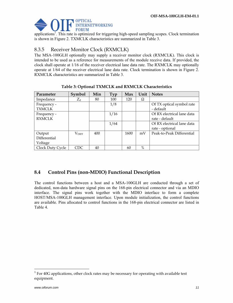
8.4.1.6 Module Low Power Pin (MOD_LOPWR) The Module Low Power pin (MOD_LOPWR) is an input from the host, operating with active-high logic. It is pulled up in the MSA-100GLH. When MOD_LOPWR is asserted, the MSA-100GLH shall be in the low power state and will stay in the low power state as long as it is asserted. When de-asserted, the MSA-100GLH shall initiate the High-Power-Up process. In Low Power mode, the MSA-100GLH shall communicate via the MDIO management interface. While the module is in Low Power mode, it has a maximum power consumption of 6W. The timing diagram for the MOD_LOPWR pin is illustrated in Figure 4. Values for t_MOD_LOPWR_on and t_ MOD_LOPWR_off are application specific and not specified in this IA.
OIF-MSA-100GLH-EM-01.1
www.oiforum.com 14
Figure 4: Module Low Power (MOD_LOPWR) Timing Diagram
8.4.1.7 Module Reset Pin (MOD_RSTn) The Module Reset pin (MOD_RSTn) is an input from the host, operating with active-low logic. This pin is pulled down in the MSA-100GLH. When MOD_RSTn is asserted (driven low), the MSA-100GLH enters the Reset state. When de-asserted, the MSA-100GLH exits the Reset state and shall begin an initialization process as part of the overall module start-up sequence. 8.5 Alarm Pins (non-MDIO) Functional Description Alarm indications from the MSA-100GLH to the host are conducted through a set of dedicated, non-data hardware signal pins on the 168-pin electrical connector and via an MDIO interface. The signal pins work together with the MDIO interface to form a complete HOST/MSA-100GLH management interface. Upon module initialization, the alarm indication functions are available. Pins allocated to alarm functions in the 168-pin electrical connector are listed in Table 5.
OIF-MSA-100GLH-EM-01.1
www.oiforum.com 15
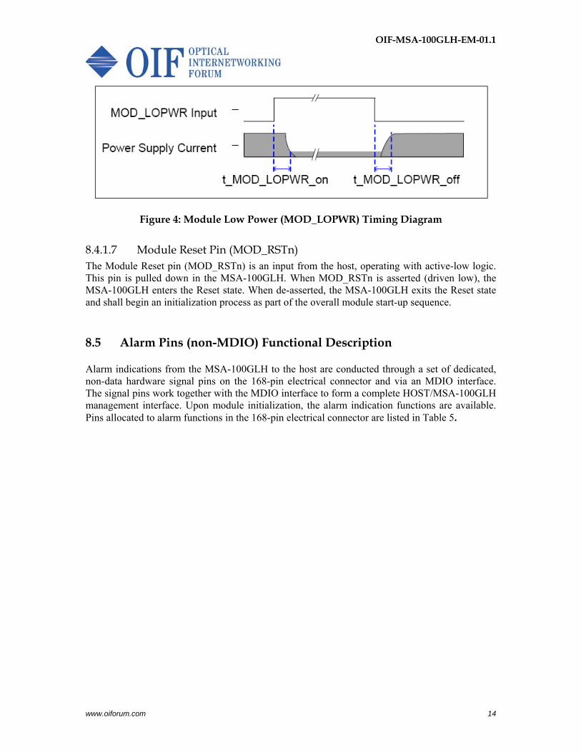
Table 5: MSA-100GLH Alarm Pins (non-MDIO)
Pin #
Symbol Description I/O
Logic “H” “L” Pull-up/down
B16 PRG_ALRM1 Programmable Alarm 1 set over MDIO
O 3.3V LVCMOS
B15 PRG_ALRM2 Programmable Alarm 2 set over MDIO
O 3.3V LVCMOS
B14 PRG_ALRM3 Programmable Alarm 3 set over MDIO
O 3.3V LVCMOS
B8 RX_LOS Receiver Loss of Signal O 3.3V LVCMOS
LOS OK
A78 MOD_ABS Module Absent “0”: module present “1” or NC: module absent
O GND Absent Present Pull-Down1
B7 GLB_ALRMn Global Alarm O 3.3V LVCMOS w/ Open Drain
OK Alarm Note 2
Note 1: Pull-down resistor (<100Ohm) is located within the MSA-100GLH. A Pull-Up resistor should be located on the host. Note 2: Pull-Up resistor on host. 8.5.1 Programmable Alarm Pins (PRG_ALRMs) The Programmable Alarm pins enable the host system to program MSA-100GLH supported alarms to dedicated hardware pins.
8.5.1.1 Programmable Alarm 1 Pin (PRG_ALRM1) Programmable Alarm 1 Pin (PRG_ALRM1) is an output to the host, operating with programmable logic. It can be re-programmed over MDIO registers to another MDIO alarm register while the MSA-100GLH is in any steady state except Reset. The default function is High Power On (HIPWR_ON) indicator with active-high logic.
8.5.1.2 Programmable Alarm 2 Pin (PRG_ALRM2) Programmable Alarm 2 Pin (PRG_ALRM2) is an output to the host, operating with programmable logic. It can be re-programmed over MDIO registers to another MDIO alarm register while the MSA-100GLH is in any steady state except Reset. The default function is Module Ready (MOD_READY) indicator with active-high logic. The default function MOD_READY is used by the MSA-100GLH during the module initialization. When asserted, it indicates the MSA-100GLH has completed the necessary initialization process and is ready to transmit and receive data.
8.5.1.3 Programmable Alarm 3 Pin (PRG_ALRM3) Programmable Alarm 3 Pin (PRG_ALRM3) is an output to the host, operating with programmable logic. It can be re-programmed over MDIO registers to another MDIO alarm register while the MSA-100GLH is in any steady state except Reset. The default function is Module Fault (MOD_FAULT) indicator with active-high logic.

OIF-MSA-100GLH-EM-01.1
www.oiforum.com 16
The default function MOD_FAULT is used by the MSA-100GLH during module initialization. When asserted, it indicates the MSA-100GLH has entered into a fault state. 8.5.2 Receiver Loss of Signal Pin (RX_LOS) The Receiver Loss of Signal pin (RX_LOS) is an output to the host, operating with active-high logic. When asserted, it indicates received optical power in the MSA-100GLH is lower than the expected value. The optical power at which RX_LOS is asserted is application specific and specified by the host system or module vendor. The timing diagram for the RX_LOS pin is illustrated in Figure 5. Values for t_loss_on and t_ loss_off are application specific and not specified in this IA.
Figure 5: Receiver Loss of Signal (RX_LOS) Timing Diagram
8.5.3 Module Absent Pin (MOD_ABS) The Module Absent (MOD_ABS) pin is an output from the MSA-100GLH to the host. It is pulled up on the host board and is pulled down to ground in the MSA-100GLH. MOD_ABS asserts a “Low” condition when the MSA-100GLH is plugged into a host socket. MOD_ABS is asserted “High” when the MSA-100GLH is physically absent from a host socket. 8.5.4 Global Alarm Pin (GLB_ALRMn) The Global Alarm pin (GLB_ALRMn) is an output to the host, operating with active-low logic. When GLB_ALRMn is asserted (driven low), it indicates that a Fault/Alarm/Warning/Status (FAWS) condition has occurred. It is driven by the logical OR of all fault, alarm, warning and status conditions latched in the latched registers. Masking Registers are provided so that GLB-ALRMn may be programmed to assert only for specific fault/alarm/warning/status conditions. It is recommended that the host board be designed to support high-priority event handling service to respond to the assertion of this pin. Upon the assertion of this pin, the host event handler identifies the source of the fault by reading the latched registers over the MDIO interface. The reading action clears the latched registers, which in turn causes the MSA-100GLH to de-assert (driven high) the GLB_ALRMn pin. The timing diagram for the GLB_ALRMn pin is illustrated in Figure 6. Values for t_GLB_ALRM_on and t_ GLB_ALRMn_off are application specific and not specified in this IA.

OIF-MSA-100GLH-EM-01.1
www.oiforum.com 17
Figure 6: Global Alarm (GLB_ALRMn) Timing Diagram
Note: In this Figure the Fault Occurrence is shown transitioning to a “Normal” status. In order for this transition to occur, a read of the alarm register must have occurred such that the fault has been received. 8.6 Module Management Interface Pins (MDIO) Description The MSA-100GLH supports control, alarm and monitoring functions via dedicated hardware pins and via an MDIO bus. The MSA-100GLH MDIO electrical interface consists of 7 pins: 1 pin for MDIO, 1 pin for MDC, and 5 MDIO Physical Port Address pins. MDC is the MDIO clock line driven by the host. MDIO is the bidirectional data line driven by both the host and module, depending upon the data direction. Pins allocated to instantiate the MDIO interface in the MSA-100GLH electrical connector are listed in Table 6.

OIF-MSA-100GLH-EM-01.1
www.oiforum.com 18
Table 6: MSA-100GLH MDIO Management Interface Pins
Pin #
Symbol Description I/O
Logic “H” “L” Pull-up /down
A28 MDIO Management Data I/O bi-directional I/O
1.2V LVCMOS
A27 MDC MDIO Clock I 1.2V LVCMOS
B21 PRTADR0 MDIO Physical Port Address bit 0 I 1.2V LVCMOS
B22 PRTADR1 MDIO Physical Port Address bit 1 I 1.2V LVCMOS
B23 PRTADR2 MDIO Physical Port Address bit 2 I 1.2V LVCMOS
B24 PRTADR3 MDIO Physical Port Address bit 3 I 1.2V LVCMOS
B25 PRTADR4 MDIO Physical Port Address bit 3 I 1.2V LVCMOS
8.6.1 Management Data Input/Output Pin (MDIO) The MDIO specification is defined in IEEE 802.3 Clause 45 [N1]. The MSA-100GLH shall support 4.0 Mbit/s maximum data rate. The MSA-100GLH uses an MDIO with 1.2V LVCMOS logic. 8.6.2 Management Data Clock Pin (MDC) The host specifies a maximum MDC rate of 4.0 MHz and MSA-100GLH hence shall support a maximum MDC rate up to 4.0 MHz. The timing diagram for the MDIO and MDC pins is illustrated in Figure 7: Module MDIO & MDC Timing Diagram
The MSA-100GLH shall support a minimal setup (tsetup) and hold (thold) time in its MDIO implementation (see Table 9).

OIF-MSA-100GLH-EM-01.1
www.oiforum.com 19
Figure 7: Module MDIO & MDC Timing Diagram
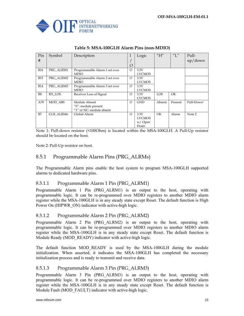
Note: Measured at Module MDIO & MDC pins. 8.6.3 MDIO Physical Port Address Pins (PRTADRs) The MDIO Physical Port Address pins (PRTADRs) are used by the host system to address all of the MSA-100GLHs contained within its management domain. PRTADR0 corresponds to the LSB in the physical port addressing scheme. The 5-pin Physical Port Address lines are driven by the host to set the module Physical Port Address which should match the address specified in the MDIO Frame. It is recommended that the Physical Port Addresses not be changed while the MSA-100GLH is powered on. 8.7 Hardware Signaling Pin Electrical Specifications 8.7.1 Control & Alarm Pins: 3.3V LVCMOS Electrical Characteristics The hardware control and alarm pins specified as 3.3V LVCMOS functionality described above shall meet the electrical characteristics described in Table 7. Figure 8 illustrates the recommended reference pin input and output terminations.
Table 7: 3.3V LVCMOS Electrical Characteristics
Parameter Symbol Min Typ Max Unit Supply Voltage VCC 3.2 3.3 3.4 V Input High Voltage VIH 2 - VCC+0.3 V Input Low Voltage VIL -0.3 - 0.8 V Input Leakage Current IIN -10 - +10 µA Output High Voltage (IOH=-100 µA) VOH VCC-0.2 - - V Output Low Voltage (IOL= 100 µA) VOL - - 0.2 V
OIF-MSA-100GLH-EM-01.1
www.oiforum.com 20
Figure 8: Reference +3.3V LVCMOS Input/Output Terminations
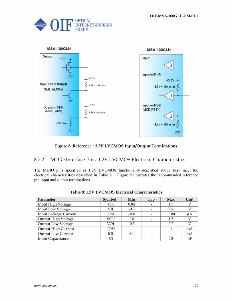
8.7.2 MDIO Interface Pins: 1.2V LVCMOS Electrical Characteristics The MDIO pins specified as 1.2V LVCMOS functionality described above shall meet the electrical characteristics described in Table 8. Figure 9 illustrates the recommended reference pin input and output terminations.
Table 8: 1.2V LVCMOS Electrical Characteristics
Parameter Symbol Min Typ Max Unit Input High Voltage VIH 0.84 - 1.5 V Input Low Voltage VIL -0.3 - 0.36 V Input Leakage Current IIN -100 - +100 µA Output High Voltage VOH 1.0 - 1.5 V Output Low Voltage VOL -0.3 - 0.2 V Output High Current IOH - - -4 mA Output Low Current IOL +4 - - mA Input Capacitance Ci - - 10 pF

OIF-MSA-100GLH-EM-01.1
www.oiforum.com 21
Figure 9: Reference MDIO Interface Termination
Note: MDC pull-up resistor is optional. Note: Host termination resistor value of 560 Ohms is recommended. This value provides the best balance of performance for both open-drain and active tri-state driver in the module. Host termination resistor values below 560 Ohms are allowed, to a minimum of 250 Ohms, but this degrades driver performance. Host termination resistor values above 560 Ohms are allowed, but this degrades open-drain driver performance. 8.8 Hardware Signaling Pin Timing Specifications The MSA-100GLH is designed to have a tightly coupled interface with host systems. A simplified overview of the recommended start-up sequence is illustrated in Figure 10. This Figure indicates steady state conditions, transient state conditions and associated signaling flags to indicate state transitions. A complete description is defined in the MDIO management interface specification [I5].

OIF-MSA-100GLH-EM-01.1
www.oiforum.com 22
Figure 10: MSA-100GLH Simplified Start-Up Flow Diagram
The MSA-100GLH is designed to support a range of optical transport applications. Many of the timing parameters associated with the module hardware control and alarm pins are application specific and thus are not specified in this IA. A summary of the timing parameters for the MSA-100GLH is given in Table 9.
Table 9: Hardware Signaling Pins Timing Parameters Summary
Parameter Symbol Min Max Unit Notes Transmitter Disabled (TX_DIS asserted)
t_off Application specific. Defined by module vendor.
Transmitter Enabled (TX_DIS de-asserted)
t_on Application specific. Defined by module vendor.
MOD_LOPWR on t_MOD_LOPWR_on Application specific. Defined by module vendor.
MOD_LOPWR off t_MOD_LOPWR_off Application specific. Defined by module vendor.
Module Reset Assert MOD_RSTn Application specific. Defined by module vendor.
Module Reset De-assert MOD_RSTn Application specific. Defined by module vendor.
Module Absent MOD_ABS Application specific. Defined by module vendor.
Receiver Loss of Signal Assert Time
t_loss_on Application specific. Defined by module vendor.
Receiver Loss of Signal t_loss_off Application specific.

OIF-MSA-100GLH-EM-01.1
www.oiforum.com 23
De-assert Time Defined by module vendor.
Global Alarm Assert Delay Time
t_GLB_ALRMn_on This is a logical “OR” of associated MDIO alarm & status registers. See MDIO spec for details.
Global Alarm De-assert Delay Time
t_GLB_ALRMn_off This is a logical “OR” of associated MDIO alarm & status registers. See MDIO spec for details.
Management Interface Clock Period
tprd 250 ns MDC is 4 MHz rate; duty cycle = 50% ± 10% (typ.)
Host MDIO setup time tsetup 10 ns Host MDIO hold time thold 10 ns Module MDIO delay time
tdelay 175 ns
Performance Monitoring Synchronization (PM_SYNC) (optional)
Default period=1 sec. ; min high/low time = 100msec.
9 Mechanical Specifications 9.1 Mechanical Overview The MSA-100GLH is designed to be assembled into a host system line card. The MSA-100GLH is electrically connected to the host line card by a 168 position connector specified herein and is physically fastened to the host line card by mounting screws through the host line card PCB. The MSA-100GLH supports two optical fiber pigtails, one for optical transmit and one for optical receive. These optical fiber pigtails are terminated and attached to host line card face plate. The MSA-100GLH is not designed to be hot-pluggable. Its power and initialization sequencing in the host line card are specified by the host line card and transponder vendors. 9.2 Electrical Connector The Hirose FX10A-168P/S-SV(83) connector assembly [N3] is specified for the host line card – MSA-100GLH electrical connector. This connector is a two component (header, receptacle), 168 position, board mounted style assembly. It meets CEI-11G-MR [N2] signal integrity performance and provides 4mm - 8mm mated stack height flexibility by header component changes only, i.e. the MSA-100GLH receptacle component remains fixed. Detailed mechanical specifications and layout design application notes may be found at [N3]. The Hirose FX10B-168P/S-SV(83) connector assembly [N3] is also specified as an option for the host line card – MSA-100GLH electrical connector. The FX10A connector style has guidepost

OIF-MSA-100GLH-EM-01.1
www.oiforum.com 24
features whereas the FX10B style does not. The FX10A and FX10B components are mate compatible and may be interchanged. Manufacturers can select either FX10A or FX10B version as appropriate for their design flow. 9.2.1 Module Electrical Connector The MSA-100GLH electrical connector is the Hirose FX10A-168S-SV(83) receptacle connector assembly[N3] illustrated in Figure 11. Pin orientation is also indicated in Figure 11. The Hirose FX10B-168S-SV(83) receptacle is also an option for the MSA-100GLH electrical connector.
Figure 11: Hirose FX10A-168S-SV(83) Receptacle Connector Assembly
9.2.2 Host Electrical Connector The host line card electrical connector is the Hirose FX10A-168P-SV(83) header connector assembly[N3] illustrated in Figure 12. Pin orientation is also indicated in Figure 12. The Hirose FX10B-168P-SV(83) header is also an option for the host line card electrical connector.

OIF-MSA-100GLH-EM-01.1
www.oiforum.com 25
Figure 12: Hirose FX10A-168P-SV(83) Header Connector Assembly
9.2.3 Host-Module Connector Alignment For alignment of host – MSA 100GLH connector mating, misalignment should be smaller that the maximum allowable misalignment value of the connector (CN) mating. Maximum gap between the connector guide pin (GP) and the PCB guide pin hole (GH) is:
CN theofnt misalignme Maximum2
Gap Maximum
≤−
=GPGH φφ
to assure CN mating after inserting guide pins into the guide pin hole. If
CN theofnt misalignme Maximum2
Gap Maximum
≥−=
GPGH φφ
this may cause connector and contact deformation. Tolerance of GP and GH is defined in Figure 13. Maximum allowable misalignment should be ≤0.42mm for FX10.

OIF-MSA-100GLH-EM-01.1
www.oiforum.com 26
Figure 13: FX10 Connector Alignment
9.3 Module Dimensions Two options are specified for the MSA-100GLH mechanical dimensions:
1) Flattop 2) Integrated Heat Sink
The flattop option is specified to allow customization of the MSA-100GLH bolt-on heat sink for supporting a wide array of optical transport applications. With this option, the bolt-on heat sink is specified by the host system designer, allowing maximum flexibility in their system design while maintaining a common module form factor. The integrated heat sink option is specified to simplify the host system design and supports module thermal performance per the maximum power consumption specified in Section 8.2. Mechanical dimensions of the MSA-100GLH with non-conductive sheet are specified in Figure 14. If a non-conductive sheet is used, the thickness is specified as 0.15 +/- 0.05mm.
Maximum Gap should be
Maximum allowable misalignment of the FX10
αφ ±GP
βφ ±GH
χ±pitchpin Guide
δ±pitch holepin Guide
ε±accuracy mounting CN
ϕ±accuracy mounting CN
αφ ±GP
βφ ±GH
χ±pitchpin Guide
δ±pitch holepin Guide
ε±accuracy mounting CN
ϕ±accuracy mounting CN
( ) ( ) ϕεδχαφβφ+++≥
+−=
2GP-GH
Gap Maximum
( )( )
22
2GP-GH
2GPGHβαϕεδχφφβαϕεδχφφ
++×+++≥
++×++++≥
( ) CN theofnt misalignme Maximum2
2≤
++×+++ βαϕεδχ
( ) 03.02
2≤
++×+++ βαϕεδχ [mm] 0.42

OIF-MSA-100GLH-EM-01.1
www.oiforum.com 27
Figure 14: MSA-100GLH Non-conductive Sheet Dimensions
Note: The module vendor must ensure the module connector receptacle component is placed to enable the module to properly mate with the host connector header when the minimum height header component (i.e. C=4mm) is used by the host. 9.3.1 Flattop Mechanical dimensions of the MSA-100GLH flattop module are specified in Figure 15. The maximum module size is specified as: 127.0mm x 177.8mm (5” x 7”) Figure 15 also specifies the receptacle connector position, connector guide pin locations and module mounting hole locations.
Module and Host PCB dimensions and tolerances in mm.
MSA Module PCB
Host PCB
Header Recept.
Sheet Thickness : S +/- s Module base: B +/- b Conn. stacking height: C +/- c Solder paste thickness: P +/- p
MSA Module
B P
S C

OIF-MSA-100GLH-EM-01.1
www.oiforum.com 28
Figure 15: MSA-100GLH Flattop mechanical dimensions - bottom/side views
The module heat sink mounting hole locations for the flattop option are specified in Figure 16. These mounting holes are not applicable to the MSA-100GLH with an integrated heat sink.

OIF-MSA-100GLH-EM-01.1
www.oiforum.com 29
Figure 16: MSA-100GLH Flattop mechanical dimensions - top view
9.3.2 Integrated Heat Sink Mechanical dimensions of the MSA-100GLH with integrated heat sink are specified in Figure 17. The maximum module size is specified as: 127.0mm x 177.8mm (5” x 7”) Figure 17 also specifies the receptacle connector position, connector guide pin locations and module mounting hole locations.

OIF-MSA-100GLH-EM-01.1
www.oiforum.com 30
Figure 17: Mechanical Dimensions of MSA-100GLH with Integrated Heat Sink
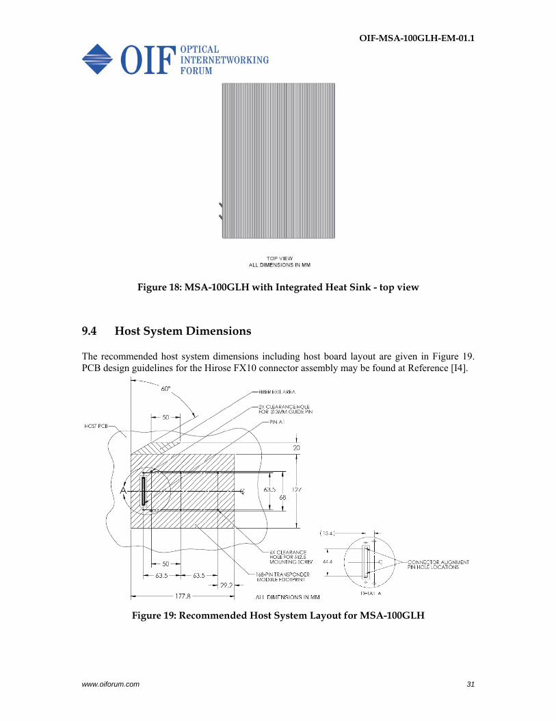
The top view of the MSA-100GLH is illustrated in Figure 18. The integrated heat-sink fin orientation and dimensions are module-vendor specific and are not specified in this document. However, the module height is required to fit within the maximum height dimension specified in Figure 17.
OIF-MSA-100GLH-EM-01.1
www.oiforum.com 31
Figure 18: MSA-100GLH with Integrated Heat Sink - top view
9.4 Host System Dimensions The recommended host system dimensions including host board layout are given in Figure 19. PCB design guidelines for the Hirose FX10 connector assembly may be found at Reference [I4].
Figure 19: Recommended Host System Layout for MSA-100GLH

OIF-MSA-100GLH-EM-01.1
www.oiforum.com 32
9.5 Module Optical Fiber Ports The MSA-100GLH optical transmit and receive fiber pigtail port location, dimensions and orientation are specified in Figure 20. The fiber pigtail type, length and connector type parameters are vendor specified and not specified in this document. The fiber boot exit area is solely for the purpose of indicating where the fibers are to exit the module side-wall at 30° ± 3° with fiber boots for strain relief.
Figure 20: MSA-100GLH Optical Fiber Port Location and Dimensions
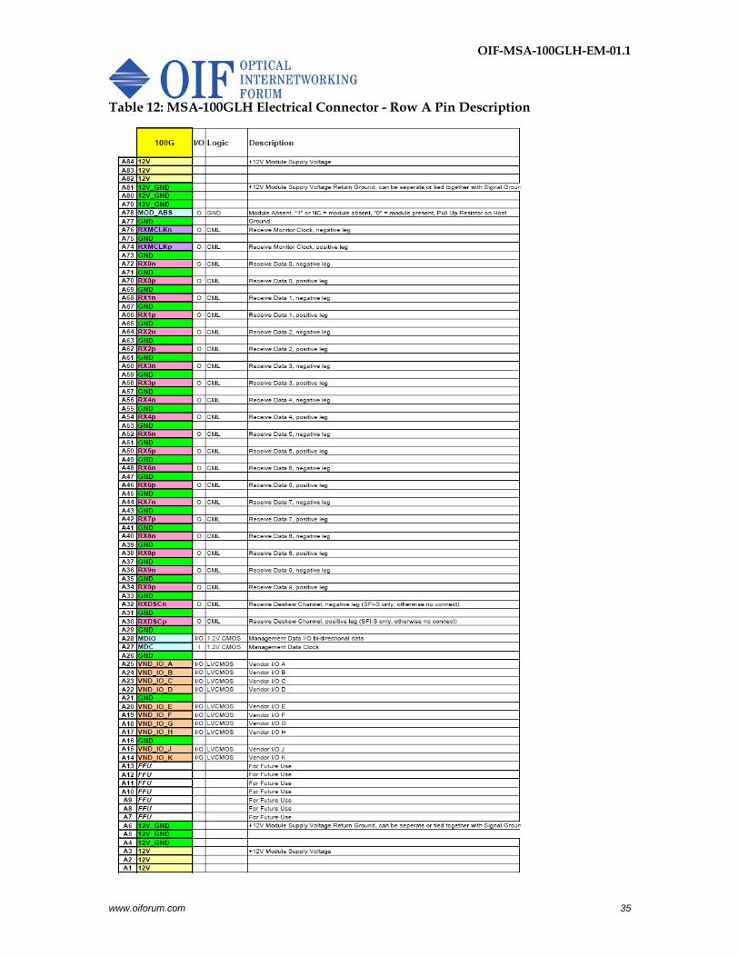
9.6 Pin Assignment The MSA-100GLH electrical connector has 168 pin positions that are arranged in a dual-row assembly. The pin assignment is specified in Table 10. Detailed description of the pin assignment is given in Table 11 and Table 12. The pin orientation is illustrated in Figure 17.
A pin map for 40G applications is given in informative Appendix D.
An optional pin-map for increasing 100G module +12v power supply is given in informative Appendix E.

OIF-MSA-100GLH-EM-01.1
www.oiforum.com 33
Table 10: MSA-100GLH Pin-Map

OIF-MSA-100GLH-EM-01.1
www.oiforum.com 34
Table 11: MSA-100GLH Electrical Connector - Row B Pin Description
OIF-MSA-100GLH-EM-01.1
www.oiforum.com 35
Table 12: MSA-100GLH Electrical Connector - Row A Pin Description
OIF-MSA-100GLH-EM-01.1
www.oiforum.com 36
10 References 10.1 Normative references [N1] IEEE 802.3ba™ -2010 “Amendment: Media Acces Control Parameters, Physical Layers and Management Parameters for 40Gb/s and 100Gb/s Operation”, Clause 45 – MDIO (March, 2010) [N2] OIF-CEI-02.0 - Common Electrical I/O (CEI) - Electrical and Jitter Interoperability agreements for 6G+ bps and 11G+ bps I/O (February 2005) [N3] Hirose FX10 Datasheets: http://www.hiroseusa.com/Special_downloads18.asp 10.2 Informative references [I1] OIF-FD-100G-DWDM-01.0 - 100G Ultra Long Haul DWDM Framework Document (June 2009) [I2] ITU-T Rec. G.709/Y.1331 (draft revised v3.4 – Oct. 2009) Interfaces for the Optical Transport Network (OTN) [I3] OIF-SFI-S-01.0 – Scalable Serdes Framer Interface (SFI-S): Implementation for Interfaces Beyond 40G for Physical Layer Devices (Nov. 2008) [I4] Hirose FX10 PCB Routing Guideline: http://www.hiroseusa.com/FX10_PCB_routing_guideline_v1.1.pdf [I5] CFP MSA Management Interface Specification V2.0, r07 (June 30, 2011) 11 Appendix A: Glossary ADC Analog Digital Converter CDR Clock and Data Recovery CN Connector CML Current Mode Logic CMOS Complementary Metal Oxide Semiconductor DEC Decoder DSP Digital Signal Processor DWDM Dense Wavelength Division Multiplex ENC Encoder FEC Forward Error Correction FFU For Future Use Gbaud 109 Symbols Per Second GH Guide pin Hole GND Ground GP Guide Pin IA Implementation Agreement LVCMOS Low Voltage CMOS MDC Management Data Clock MDIO Management Data Input/Output NC No Connect OIF Optical Internetworking Forum OTL Optical channel Transport Lane PCB Printed Circuit Board PM-QPSK Polarization Multiplexed Quaternary Phase Shift Keying RX Receiver

OIF-MSA-100GLH-EM-01.1
www.oiforum.com 37
SFI Serdes Framer Interface TX Transmitter VND Vendor 12 Appendix B: Open Issues / current work items None.

OIF-MSA-100GLH-EM-01.1
www.oiforum.com 38
13 Appendix C: List of companies belonging to OIF when
document is approved Acacia Communications IP Infusion
ADVA Optical Networking JDSU
Alcatel‐Lucent Juniper Networks
Altera KDDI R&D Laboratories
AMCC LeCroy
Amphenol Corp. Lightwire
Anritsu LSI Corporation
AT&T Luxtera
Avago Technologies Inc. Macom Technology Solutions
Broadcom Marben Products
Brocade Mayo Clinic
Centellax, Inc. Metaswitch
China Telecom Mitsubishi Electric Corporation
Ciena Corporation Molex
Cisco Systems MoSys, Inc.
ClariPhy Communications NEC
Cogo Optronics NeoPhotonics
Comcast Nokia Siemens Networks
Cortina Systems NTT Corporation
CyOptics Oclaro
Department of Defense Opnext
Deutsche Telekom Picometrix
ECI Telecom Ltd. PMC Sierra
Emcore QLogic Corporation
Ericsson Semtech
ETRI SHF Communication Technologies
EXFO Sumitomo Electric Industries
FCI USA LLC Sumitomo Osaka Cement
Fiberhome Technologies Group TE Connectivity
Finisar Corporation Tektronix
Force 10 Networks Telcordia Technologies
France Telecom Tellabs
Fujitsu TeraXion
Furukawa Electric Japan Texas Instruments Iain Robertson
Gennum Corporation Time Warner Cable
GigOptix Inc. TriQuint Semiconductor
Hewlett Packard u2t Photonics AG

OIF-MSA-100GLH-EM-01.1
www.oiforum.com 39
Hitachi Verizon
Hittite Microwave Corp Vitesse Semiconductor
Huawei Technologies Xilinx
IBM Corporation Xtera Communications
Infinera Yamaichi Electronics Ltd.
Inphi ZTE Corporation

OIF-MSA-100GLH-EM-01.1
www.oiforum.com 40
14 Appendix D (informative): Pin Map Allocation for 40G
Applications This appendix specifies the MSA-100GLH 168-pin electrical pin allocation for 40G applications. This pin map is compatible with the 100G applications pin-map specified in the normative sections of this IA and supports OTL3.4 interfaces.

OIF-MSA-100GLH-EM-01.1
www.oiforum.com 41
Table 13: MSA-100GLH Electrical Connector - Row B Pin Map (40G Application)

OIF-MSA-100GLH-EM-01.1
www.oiforum.com 42
Table 14: MSA-100GLH Electrical Connector - Row A Pin Map (40G Application)

OIF-MSA-100GLH-EM-01.1
www.oiforum.com 43
15 Appendix E (informative): Optional Pin Map Allocation for 100G Applications
This Informative Appendix specifies an alternative electrical pin allocation that may optionally be used for increasing +12V power supply for 100G module applications. MSA-100GLH Electrical Connector Row B pin allocation is per specification given in Section 9.6/Table 11. MSA-100GLH Electrical Connector Row A pin allocation is per specification given in below Table 15.

OIF-MSA-100GLH-EM-01.1
www.oiforum.com 44
Table 15: MSA-100GLH Electrical Connector - Row A Pin Description Option
- End of Document -