The L0 Calorimeter Trigger U. Marconi On behalf of the Bologna Group CSN1, Catania 16/9/02.
33
The L0 Calorimeter Trigger U. Marconi On behalf of the Bologna Group CSN1, Catania 16/9/02
-
Upload
owen-williams -
Category
Documents
-
view
224 -
download
0
Transcript of The L0 Calorimeter Trigger U. Marconi On behalf of the Bologna Group CSN1, Catania 16/9/02.

The L0 Calorimeter Trigger
U. Marconi
On behalf of the Bologna Group
CSN1, Catania 16/9/02
INFN Sezione di Bologna
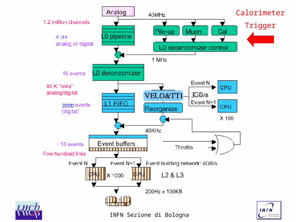
Calorimeter
Trigger

INFN Sezione di Bologna
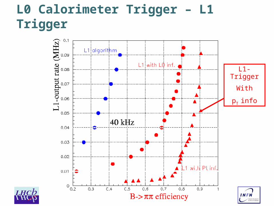
LHCb Trigger Performances
L1 Trigger
using
L0 information
INFN Sezione di Bologna
L0 Calorimeter Trigger – L1 Trigger
L1-Trigger
With
pT info

INFN Sezione di Bologna
Identify hot spots Detect a high energy in a small surface Use a square of 2 x 2 cells area
8 x 8 cm2 in the central region of ECAL (may loose a few % of the energy)
more than 50 x 50 cm2 in the outer region of HCAL
Select the particles with the highest ET
Due to its high mass, a B particle decays into high PT particles
'High PT ' is a few GeV
For the Level 0 decision, we need the particle with the highest PT (the second highest also in HCAL)
Calorimeter Trigger Basic Principles

INFN Sezione di Bologna
Select locally the highest candidate (reducing complexity and cabling) Process further only the local candidates
~200 for ECAL and ~50 for HCAL starting from 6000 and 1500 cells.
Validate the candidates Electron, photon, 0:
Electromagnetic nature using the PreShower
Charge using the SPD
Hadron
Add the energy lost in ECAL in front of the HCAL candidate, looking only at ECAL candidates (manageable number of connections)
INFN Sezione di Bologna
Select the highest validated candidates One wants the highest ET candidates
Ghosts removal
Second highest for hadrons
No need for a second highest for electron or photon.
The processing is entirely synchronous No dependence on occupancy and history
Easier to understand and to debug
Pipeline processing at all stages.
INFN Sezione di Bologna
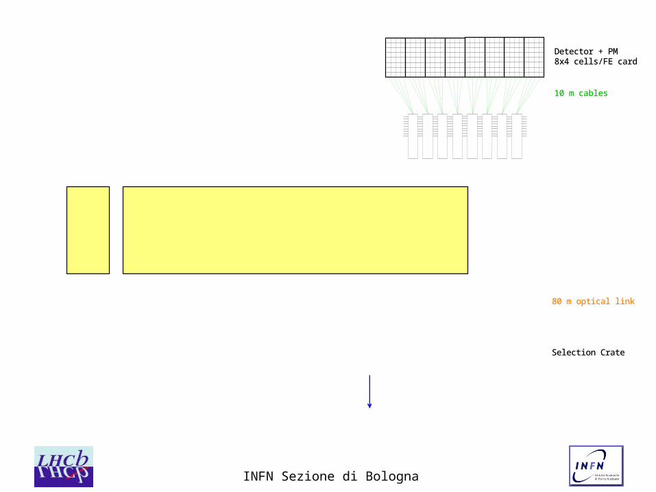
Detector + PM8x4 cells/FE card
10 m cables
80 m optical link
Selection Crate
Pla
tform
on
top
of ca
lorim
ete
r
LVDS links
14 ECAL crates 4 HCAL cartes 8 Prs/SPD crates 8 cards per half crate
FE
FE
FE
FE
FE
FE
FE
FE
Ba
rrack
LVDS links
L0 Decision Unit
80 inputs
TotalEnergy
FE
FE
FE
FE
FE
FE
FE
FE
HighestElectron
HighestPhoton
ECAL HCAL
HighestHadron
SecondHighest
Highestlocal
80 linksfrom 50 cards
8 inputs 4 inputs
28 inputs
4 outputs
One Validation card per half ECAL crateOne SPD sum perhalf PreShower crate
FE
PreShower / SPD
AddressFE
FE
FE
Validation Card
LUT
highestelectron
highestphoton
28 inputs
highest
local
28 inputs
LUT
Level 0 Decision Unit
8 inputs x 8 bits
Merge back to 50
address match
highest
Highest global
highest
global
28 inputs
E TOT
8 inputsSPD
multiplicity
Add
16 inputs
SPDmultiplicity
Add

INFN Sezione di Bologna
Hardware Implementation About 6000 ECAL cells (as well as for the PreShower and the SPD)
Variable cell size, identical structure for
SPD/PreShower /ECAL HCAL different, see later
Front-end electronics located on top of the detector Use SEU immune components (order of 100 rads/year) 32 channels per FE card for ECAL/HCAL, 64 for Prs/SPD
Minimal cabling complexity Use a dedicated backplane for as many connections as
possible
8 bits ET converted from the 12 bits ADC. 8 bits are adeguate with a full scale limit around 5 GeV.

INFN Sezione di Bologna
First selection Build the 2x2 sums
Work inside a 32 channels (8x4) front-end card To obtain the 32 2x2 sums, one needs to get the 8 +
1 + 4 neighbours
Via the backplane (9) or dedicated point-to-point cables(4)
: 8 bits LVDS multiplexed link
: 8 bits on the backplane
Neighbours of each cell
INFN Sezione di Bologna
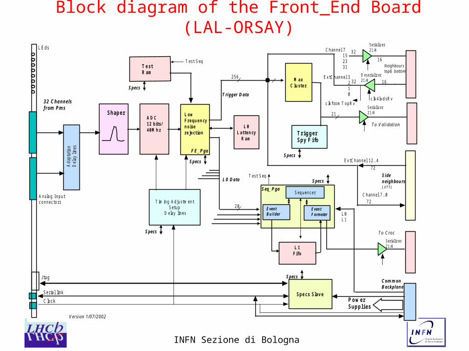
Block diagram of the Front_End Board (LAL-ORSAY)
S p e c s S lav e
Serializ er2 1 /4
E x tC h an n el 1 2 . .4
C h an n el 7 . . 0
J ta g
C loc k P o w e rSuppl i e s
L E ds
7 2
S e ria l link
Serializ er2 1 /4
3 2C h an n el 7 1 5 2 3 3 1
1 6
E x tC h an n el 3 2 1 0
3 2M a xC lu s te r
c lk f r o m T o p R vc lk 4 lv d s R v
D es erializ er2 1 /4 1 6
Shape rA D C1 2 bit s /4 0 M h z
L 0L a t te n cy
R a m
L o wFre qu e n cyn o is ere je ct io n
L 1Fifo
Serializ er2 1 /4
T im in g Ad ju s tm en tS etu p
D elay lin es
Ada
ptat
ion
Del
a y l i
n es
An a lo g I n p u tc o n n ec to r s
L 0 D a ta
T rig ger D a ta
T e s tR am
2 5 6
S id en eig h b o u rsLVTTL
7 2
C o m m o nB a ck p la n e
F E _ P g a
S pecs
S pecs
S pecs
S pecs
S pecs
L 0L 1
Tr i g g e rSpy F i fo
S eq _ P g a
N eig h b o u r sto p & b o tto m
T o C ro c
T o V a lid a tio n
2 1
S pecs
V ersio n 1 /07 /2 0 0 2
3 2 C ha nne lsfrom P m s
E ven tB u i l d er
E ven tF o rm a ter
S eq u en c er
2 0
T es t S eq
T es t S eq
INFN Sezione di Bologna
3
5
4
4
66
3
1
2
3
4
5
6
1
2
3
4
5
6
7
7
8
2 7
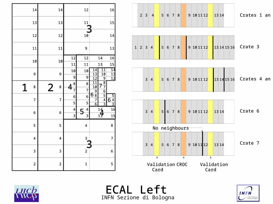
Crates 1 and 2
Crate 3
Crates 4 and 5
Crate 7
8
9
10
12
13
14
11
2
3
4
5
6
7
8
9
10
12
13
14
11 9
10
12
11
13
14
16
15
3
4
5
6
7
8
9
10
11
12
13
14
15
16
3
4
5
6
7
8
9
10
11
12
13
14
15
16
6789
1011121314
3456789
1011
121314
ValidationCard
ValidationCard
CROC
No neighbours
4 5 82 3 6 7 9 10 11 12 13 14
1 4 5 82 3 6 7 9 10 11 12 13 14 15 16
4 5 83 6 7 9 10 11 12 13 14 15 16
4 5 83 6 7 9 10 11 12 13 14
Crate 64 5 83 6 7 9 10 11 12 13 14
345
ECAL Left

INFN Sezione di Bologna
INFN Sezione di Bologna
ECAL Validation For each ECAL candidate, one needs to
access the SPD and the PreShower information (2 times 4 bits for the SPD&Preshower cells corresponding to the ECAL candidate)
The address is sent from the ECAL to the PreShower FE bords
One PreShower board handles 64 channels (exactly 2 ECAL boards)
The 24 bits are extracted synchronously at each BX and sent to the Validation Card
INFN Sezione di Bologna
ECAL Validation produces 4 candidate types Electrons and photons are validated FE-candidates
‘local 0’ is detected as a high total energy on a card
‘global 0’ is detected by summing the energies of two FE-candidates of two adjacent cards.
No SPD/PreShower validation foreseen for the 0, but this will be integrated in the card, in case…
This is just a few more output bits of the previous LUT, plus the validation of a register.
Only the highest Et ECAL candidate is interesting We select the highest of the 8 on the Validation card
Output 4 ECAL candidates Each has 8 bits Et and 8 bits address, plus BX-ID.
INFN Sezione di Bologna
HCAL Validation Ideal case: Add the ECAL cells in front of the
HCAL candidate, but this implies a lot of connections, at 40 MHz.
This addition is important only if the ECAL energy deposit is large, then likely, it also has a large chance to be detected as a local maximum in the ECAL FE-board.
Send the 50 HCAL candidates to the ECAL ones Less connections, some duplication, but we can use the
ECAL Validation Card.
One ECAL FE-board matches only one HCAL card. One validation card receives at most four HCAL cards One HCAL card goes at most (30 of 50) to two Validation
cards
INFN Sezione di Bologna
Validation board
LU T1 K 8
P S/SP D 7e /p v a lid 8
H ca l A d d 7 :020
H ca ls e l0
H ca ls e l7
5
2M u x
M u x
H c a l Se l 7 : 0
4 0
1 6
I2 C in t
5
5L U T1 K 8
A d d r e ssM a tc h
3
Ec a l A d d 7
5
5L U T1 K 8
A d d r e ssM a tc h
3
Ec a l A d d 0
A d d M a tch 7 :0
H ca l S el
E ca l 7 :0 E t 7 :0
1 6
2 4
8 H ca l 3 :2 E t 7 :0
H cal 3 :0 ad d 4 :0H ca l 3 :0 E t 7 :0
R J 4 5
M u x _ P ga
3 Vr eg
D es erial i zer2 1 /4
5 2
F ro mH ca l Cra tes
J ta g
C loc k
L E dsG
Lin
k In
t erf
a ce
S p e c s S lav eP o w e rSuppl i e s
S e ria l link
C om m o nB ackp la n e
V ersio n 1 /0 7 /20 02
1 6 8
F ro m lo ca lF e E ca l
3 2
E ca l 7 :0 E tclu s7 :0E ca l 7 :0 E t to t 7 :0E ca l 7 :0 C lu s tadd 4:0
P S /S P D 7:0 va l 7 :0P S /S P D 7:0 ad d 5 :0
F ro mP S /S P D cra tes
P C IC o n n e c to r
E ca l 7 :0 E tclu s7 :0
E ca l 7 :0 ad d 4 :04 0
6 4
D es erial i zer2 1 /4
D es erial i zer2 1 /4
1 6 8
E c a l E t 7H c a l3 a d d
8
8
3 V de c
Se lde c o de
H cal3 H c a l Se l 7
3
2
8
A d d M a tch 0
H ca l S el 0E ca l E t 0Sum
M a xC o m p
E tra n s3 -2 H ca l _ Pg a < 1 5 0 I O
H c a l 3 E t 7 : 0
H c a l 3 l o g i c
H c a l 2 l o g i c
E tra n s28
E tra n s3
5
5
H c a l 2 a d d
p ip e lin e ( h ca l log ic)20
H ca l add
A ddM a t c h 7
E tra n s1 -0 H ca l _ P g a
E tra n s185
H c a l 1 a d d
5
8E tra n s0
H c a l 0 a d d
GL
ink
Int e
rfa c
e
LU T1 K 8
P S/SP D 7e /p v a lid 8
LU T1 K 8
P S/SP D 7e /p v a lid 8
P S /S P D 7 va l 7 :0
P S /S P D 0 va l 7 :0
LU T1 K 8
P S/SP D 7e /p v a lid 8
4 2
P S /S P D 0 va l 7 :0
P S /S P D 7 va l 7 :0
E c a l7 e v a l
E c a l0 E tc lu s7 :0E c a l 0 e v a l
M a xC o m p
in ca s ca d e
6 4 E ca l 7 :0 E tS u m 7 :0
4 8
LU T1 K 8
P S/SP D 7e /p v a lid
LU T1 K 8
P S/SP D 7e /p v a lid
8
3
P i0 _ P ga
H igh es t elect ro n
H igh es t p h o t o n
G lo b al P i0
L o cal P i0
S p ecs
3 V d ec
H igh es telect ro n
E c a l7 E tc lu s7 :0E c a l7 e v a l
E c a l0 E tc lu s7 :0E c a l 0 e v a l
M a xC o m p
in ca s ca d e
a dd
E t r a n s8
8
e -p h o t p i_ P ga
E c a l7 E tc lu s7 :0
8
8H igh es tp h o t o n
E c a l7 e v a l
E c a l0 E tc lu s7 :0E c a l 0 e v a l
M a xC o m p
in ca s ca d e
4 8
E c a l7 E tc lu s7 :0
E c a l6 E tc lu s7 :0+
E c a l0 E tc lu sE c a l1 E tc lu s
p iv a l6
p iv a l0
M a xC o m p
in ca s ca d e
8
8
G lo b alP i0
8
8
P S /S P D 7 va l 7 :0
P S /S P D 0 va l 7 :0
n o t d e c id e d y e t
R J 4 5
H cal 3 :0 ad d 4 :0
8
8
6 4
E ,P ,P i,G lo P i,H calC lu s t
S p ecs
M o n i to ri n gF i fo
1 0 1
LAL ORSAY

INFN Sezione di Bologna
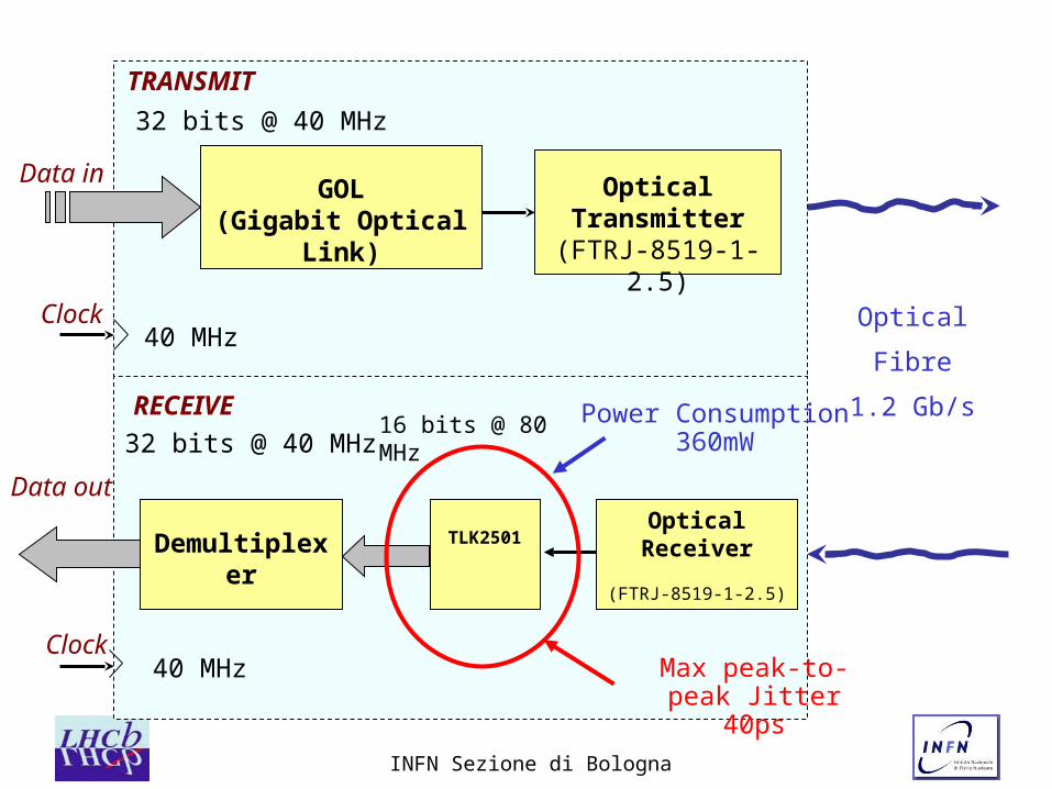
The Optical Links The Optical Links are used to transmit the
calorimeter-clusters from the Validation Cards to the Selection Crate
The total amount of the optical channels 16 (SPD) + 428 (ECAL) + 80 (HCAL) = 208 Ch
Cluster bit patterns HCAL: 8 bits (BX) + 8 bits (ET) + 5 bits (Address)
ECAL: 8 bits (BX) + 8 bits (ET) + 8 bits (Address)
SPD: 8 bits (BX) + 10 bits (Mult.)
INFN Sezione di Bologna
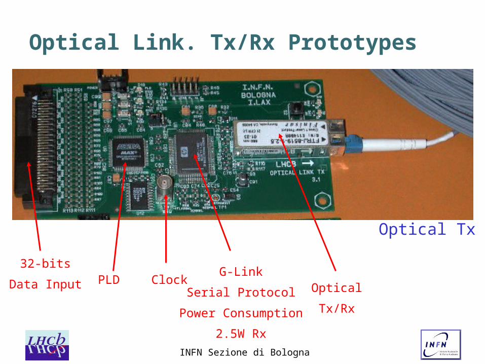
Optical Link. Tx/Rx Prototypes
ClockG-Link
Serial Protocol
Power Consumption
2.5W Rx
Optical
Tx/Rx
PLD 32-bits
Data Input
Optical Tx
INFN Sezione di Bologna
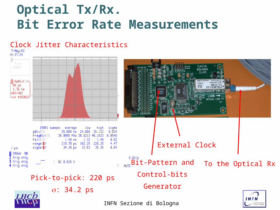
Optical Tx/Rx. Bit Error Rate Measurements
Pick-to-pick: 220 ps
: 34.2 ps
Clock Jitter Characteristics
External Clock
Bit-Pattern and
Control-bits
Generator
To the Optical Rx
INFN Sezione di Bologna
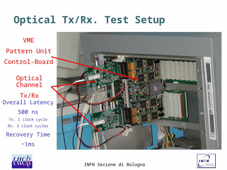
Optical Tx/Rx. Test Setup
Optical Channel
Tx/Rx
VME
Pattern Unit
Control-Board
Overall Latency
500 nsTx: 1 clock cycle
Rx: 3 clock cycles
Recovery Time
~1ms

INFN Sezione di Bologna
BER vs Jitter Glink Optical ChannelBER vs Jitter
1,00E-16
1,00E-14
1,00E-12
1,00E-10
1,00E-08
1,00E-06
1,00E-04
1,00E-02
1,00E+00
34,2 54,8 59,2 61,2 68 75,1
Jitter (ps)
BE
R
33120 Agilent
Noise Generator
Vpp(mV) 40.00 MHz
PMT5193
PG9210 LC584
Philips PM5193
Function Generator
And Modulator
Le Croy PG9210
Pulse Generator
Le Croy LC584
Oscilloscope
Ext. Modulation Ext. Trigger Sine Wave 40MHz Clock with jitter
0
20
40
60
80
100
120
140
Vpp Noise[mV]
Jitt
er
(ps)
Jitter Modulation
INFN Sezione di Bologna
Optical
Fibre
1.2 Gb/s
Optical Transmitter
(FTRJ-8519-1-2.5)
32 bits @ 40 MHz
TRANSMIT
Data in
Clock40 MHz
GOL(Gigabit Optical Link)
OpticalReceiver
(FTRJ-8519-1-2.5)
TLK2501Demultiplexer
16 bits @ 80 MHz
Data out
32 bits @ 40 MHz
RECEIVE
Clock40 MHz Max peak-to-peak
Jitter 40ps
Power Consumption 360mW
INFN Sezione di Bologna
L8
HZ0805E601R-00
i2c_addr3
conf_wmode16
R141
2.2K
SDA
a12b12c12d12
a11
a10
a9
a8
a7
a6
a5
a4
a3
a2
a1 b1
b2
b3
b4
b5
b6
b7
b8
b9
b10
b11
c1 d1
c2
c3
c4
c5
c6
c7
c8
c9
c10
c11
d2
d3
d4
d5
d6
d7
d8
d9
d10
d11
Disposizionedelle file.Lato TOP
CON2
Metrical4x12
a11
a25
a39
a413
a517
a621
a725
a829
a933
a1037
a1141
a1245
b12
b26
b310
b414
b518
b622
b726
b830
b934
b1038
b1142
b1246
c13
c27
c311
c415
c519
c623
c727
c831
c935
c1039
c1143
c1247
d14
d28
d312
d416
d520
d624
d728
d832
d936
d1040
d1144
d1248
i2c_addr4
C159
100nF
test_shift
i2c_addr6
SDA
SCLi2c_addr4
C160
10nF
i2c_addr3
i2c_addr5i2c_addr2
SCL
i2c_addr1
conf_negedge
D5LED
R12051
R132330
VDDTX
conf_glink
C170
10nF
davconf_wmode16
cav
VDD2.5TX
SW5
SW DIP-8/SM
R12151R12251R12351R12451R12551
J13
LEMO
RR4 4.7K
1 2 3 4 5 6 7 8 9
R12751R12951R13051R13151R13351R13451R13551R13651R13751R13851
C169
10nF
C171
10nF
VDD2.5TX
dav
U9
GOL
din<0>L3
serial_line_nA7
GND
A3
VDD
A1
GND
A9
GND
A10
GND
B3
GND
B6
GND
B7
GND
B8
GND
B9
GND
B10
GND
C1
GND
C10
GND
C5
GND
C6
GND
D4
GND
D7
GND
D8
GND
D9
GND
E3
GND
E9
GND
F3
GND
G10
GND
H3
GND
H9
GND
J4
GND
K1
GND
K2
GND
M3
GND
TpE5
GND
TpE6
GND
TPE7
GND
TpE8
GND
TpF5
GND
TpF6
GND
TpF7
GND
TpF8
GND
TpG5
GND
TpG6
GND
TpG7
GND
TpG8
GND
TpH5
GND
TpH6
GND
TpH7
GND
TpH8
VDD
A2
VDD
A11
VDD
A12
VDD
B1
VDD
B2
VDD
B11
VDD
B12
VDD
C7
VDD
C8
VDD
C9
VDD
D5
VDD
D6
VDD
E4
VDD
E10
VDD
F4
VDD
F9
VDD
G9
VDD
H4
VDD
H10
VDD
J5
VDD
J6
VDD
J7
VDD
J8
VDD
J9
VDD
L1
VDD
L2
VDD
L11
VDD
L12
VDD
M1
VDD
M2
VDD
M11
VDD
M12
din<1>L4
din<2>L5
din<3>M5
din<4>M6
din<5>L7
din<6>M8
din<7>M9
din<8>L9
din<9>K9
din<10>K10
din<11>J10
din<12>J11
din<13>H11
din<14>G11
din<15>F12
din<16>K5
din<17>M4
din<18>K6
din<19>L6
din<20>M7
din<21>K7
din<22>L8
din<23>K8
din<24>M10
din<25>L10
din<26>K11
din<27>K12
din<28>J12
din<29>H12
din<30>G12
din<31>F11
davF1
cavG2
serial_line_pA6
test_analogJ2
test_shiftF2
clkLHCnD11 clkLHCpC12
selectDiffC11
clkLHCD10
readyJ3
Id_cathodeA8
reset_bD1
conf_glinkC2
conf_i_Id<0>G4
conf_i_Id<1>H2
conf_i_pllB4
conf_i_laserD2
conf_negedgeD12
conf_wmode16E2
FFE11
flag<0>F10
flag<1>E12
i2c_addr<1>B5i2c_addr<2>A5i2c_addr<3>A4i2c_addr<4>C4i2c_addr<5>C3i2c_addr<6>D3SCLK3SDAK4
JTAGTCKE1
JTAGTDIH1
JTAGTMSG1
JTAGTRST_bJ1
JTAGTDOG3
cav
Title
Size Document Number Rev
Date: Sheet of
Optical Link TX RX 3.2 LHCB 0
TX GOL
I.N.F.N.Electronic Group - Bologna
Ing. Ignazio Lax
A3
3 3Wednesday, July 31, 2002
C164
4.7µF
10V
0805
selectDiff
C172
10nF
L9
HZ0805E601R-00 C162
100nF
C163
10nF
C168
4.7µF
10V
0805
VDD2.5ATX
C161
10nF
din0din1din2din3din4din5din6din7din8din9din10din11din12din13din14din15din16din17din18din19din20din21din22din23din24din25din26din27din28din29
din31din30
VDD2.5TX
conf_i_ld0conf_i_ld1
conf_i_pllconf_i_laser
flag1flag0
VDD2.5TX
SW4
SW DIP-8/SM
J8
HEADER2x32
1 23 45 67 8911131517192123
1012141618202224
25272931333537394143
26283032343638404244
45474951535557
46485052545658
596163
606264
R11651
L10
HZ0805E601R-00 C166
100nF
RR3 4.7K
1 2 3 4 5 6 7 8 9
VDD2.5TX
C167
10nF
VCCTTX
C165
10nF
VDDTX
selectDiff
VDD2.5TX
U10
MAX6315
RESET2
VCC
4GN
D1
MR3
FF
R14510K
SW6
PUSH
BUTT
ON
Q2MMBT2369A
3
1
2
R144
49.9 1%
VDD2.5TX
VCCTX
conf_i_ld0
R10149.9 1% 0402
R10749.9 1% 0402
resetTX
din0
R142open
J10
HEADER2x2
1234
resetTX
conf_i_ld1
J12
HEADER2
12
din1din2
din4din3
din6din5
din9din8din7
din10
din12din11
din13din14
din16din15
din17
din19din20
din18
din22din21
R13951
din24din25
din23
din27din26
din28
din30din29
din31
conf_i_laser
SW3
SW DIP-8/SM
VCCTTX
R10251
VDD2.5TX
R10351R10451R10551R10651R10851R10951R11051
conf_i_pllR11151R11251
i2c_addr5
R11351R11451R11551
din0
R11751
VDDTX
J14
HEAD
ER2
12
R11851R11951
din2din3
din1
din6
din4din5
din8din7
din9din10din11din12din13din14din15din16din17
din19din20
din18
din21
U8
FTRJ-8519-1-2-5
RX+5
RX-4
GND
1GN
D7
VCCR2
VCCT6
TX+9
TX-10
SD3
TDIS8
ready
din23din22
din24
din26din25
din27din28din29
din31din30
R12851
R14051
R12651
flag0
test_shift
R143
100
JTAGTMSJTAGTDIJTAGTDOJTAGTCK
JTAGTRST_b
flag1
J9
HEAD
ER7
1234567
i2c_addr6
VDD2.5ATX
FF
din[31..0]
i2c_addr1ready
conf_glink
test_analog
J11
HEAD
ER2
12
VDDTX
conf_negedge
i2c_addr2
RR2 4.7K
1 2 3 4 5 6 7 8 9
C158
10nF
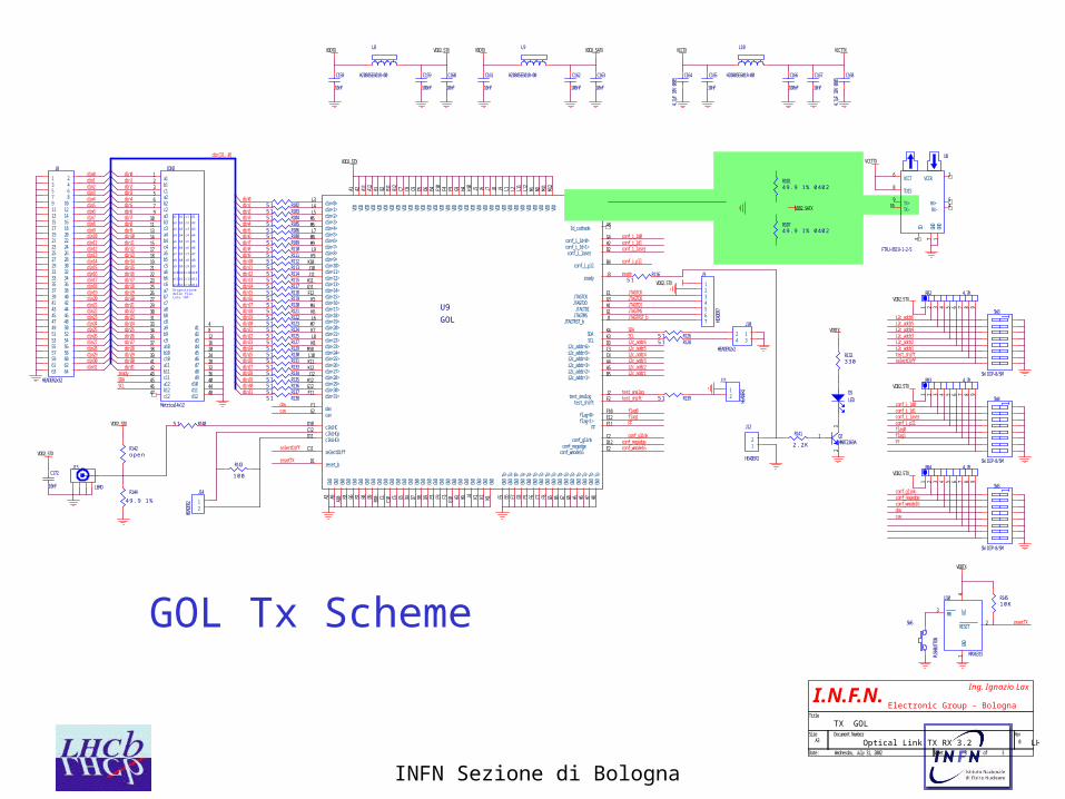
GOL Tx Scheme
INFN Sezione di Bologna
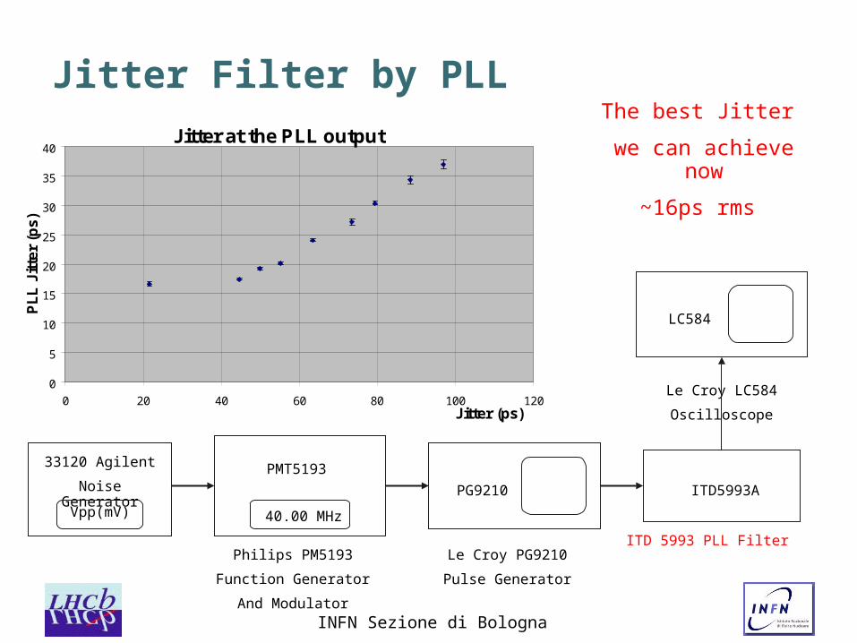
Jitter Filter by PLLJitter at the PLL output
0
5
10
15
20
25
30
35
40
0 20 40 60 80 100 120Jitter (ps)
PL
L J
itte
r (p
s)
33120 Agilent
Noise Generator
Vpp(mV) 40.00 MHz
PMT5193
PG9210
LC584
Philips PM5193
Function Generator
And Modulator
Le Croy PG9210
Pulse Generator
ITD5993A
ITD 5993 PLL Filter
Le Croy LC584
Oscilloscope
The best Jitter
we can achieve now
~16ps rms
INFN Sezione di Bologna
The Selection Crate
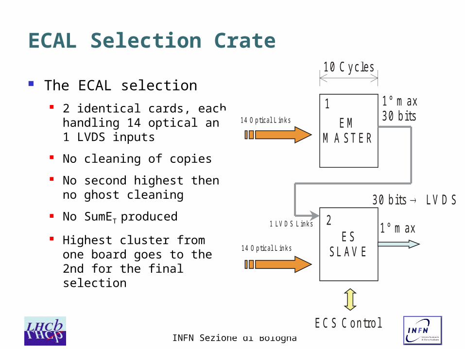
The 4 ECAL types are processed the same way The complete cluster-address assignement is performed The highest of the 28 inputs for each cluster type is
selected and sent to the L0DU
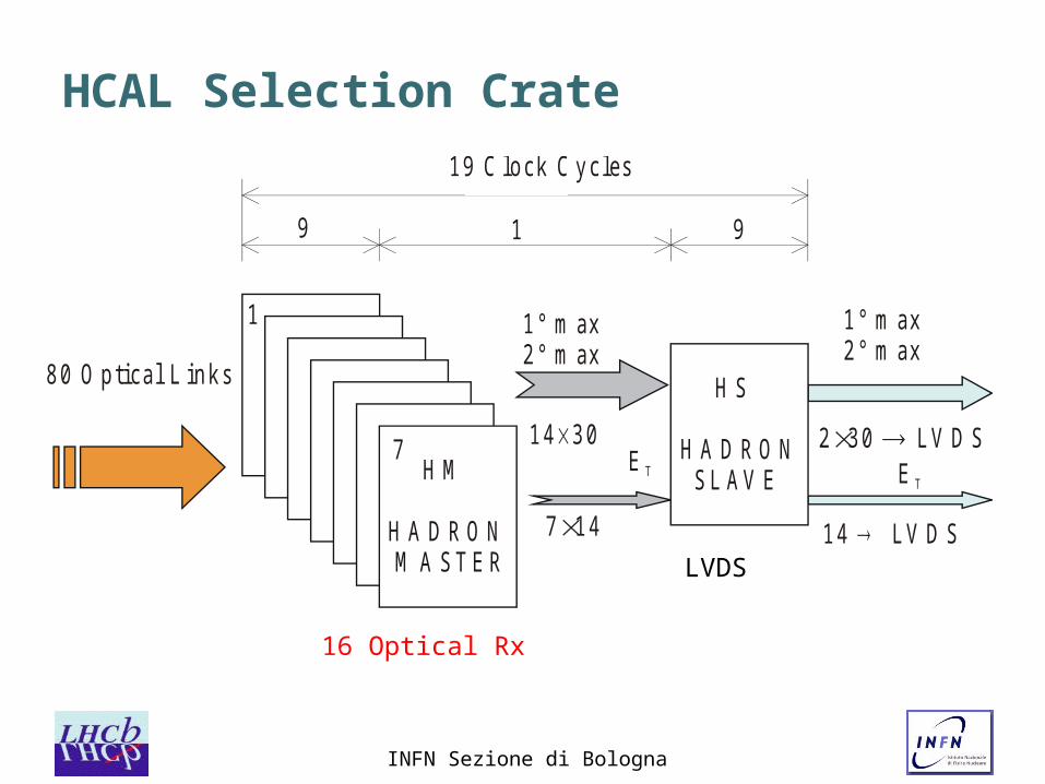
The HCAL processing Cluster copies are removed, the highest is selected The complete cluster-address is produced Ghosts are removed Cluster selection is performed to select the highest and
the 2nd highest clusters The sum of the transverse energy of the candidates is
calculated
INFN Sezione di Bologna
HCAL Selection Crate
H S B
M aste r
H S B
M a ste r
H S B
M aste r
H S B
M a ste r
M aste r
H S B
M a ste r
1 9 C lo ck C y c le s
9 1
1 ° m ax2 ° m ax
1 ° m ax2 ° m ax
1 4 3 0E T E T
7 1 4
H S
H A D R O N S L AV E H M
H A D R O N M A S T E R
8 0 O p tica l L in k s
2 3 0 LV D S
1 4 LV D S
7
1
9
16 Optical Rx
LVDS
INFN Sezione di Bologna
ECAL Selection Crate
The ECAL selection 2 identical cards, each
handling 14 optical and 1 LVDS inputs
No cleaning of copies
No second highest then no ghost cleaning
No SumET produced
Highest cluster from one board goes to the 2nd for the final selection
1 LV D S L in k s
1 4 O p tic a l L in k s
1 4 O p tic a l L in k s
E SS L AV E
E MM A S T E R
1
2
1 ° m ax3 0 b its
1 ° m ax
3 0 b its LV D S
1 0 C y c le s
E C S C o n tro l
INFN Sezione di Bologna
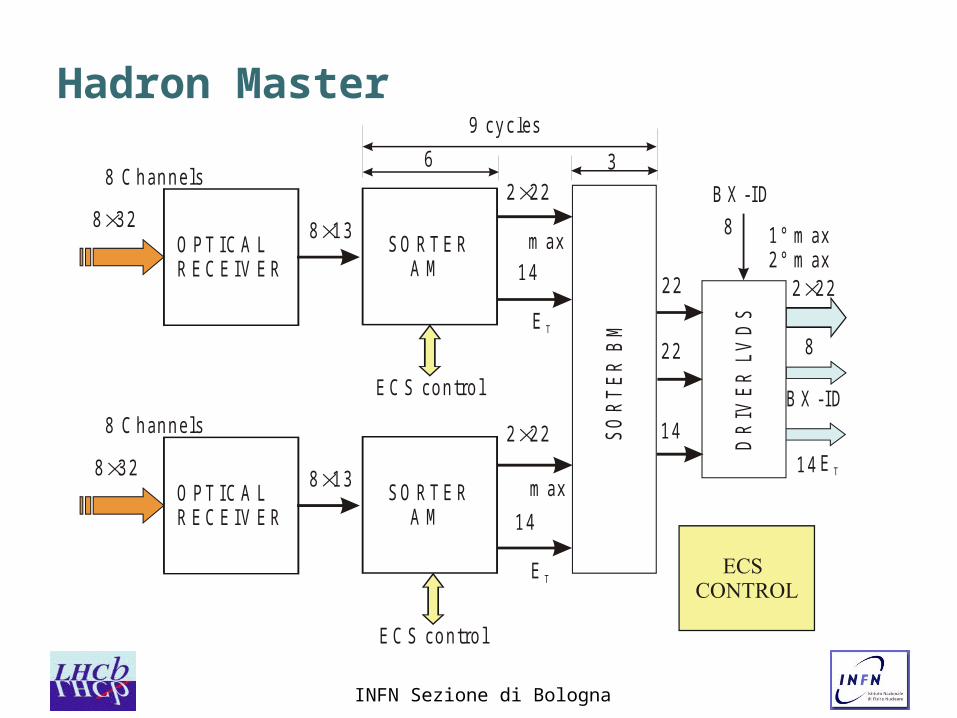
Hadron Master
DR
IVE
R L
VD
S
SO
RT
ER
BM
8 x 2 1
O P T IC A LR E C E IV E R
8 C h an n e ls
S O RT E R A M
8 1 3
2 2 2
1 4
1 4
1 4
m ax
E T
8 x 2 1
O P T IC A LR E C E IV E R
8 C h an n e ls
E C S co n tro l
E C S co n tro l
S O RT E R A M
8 1 38 3 2
8 3 2
2 2 2
2 2
2 2
2 2 21 4
m ax
E T
E T
1 ° m ax2 ° m ax
B X -ID
B X -ID
8
9 cy c le s
6 3
8
INFN Sezione di Bologna
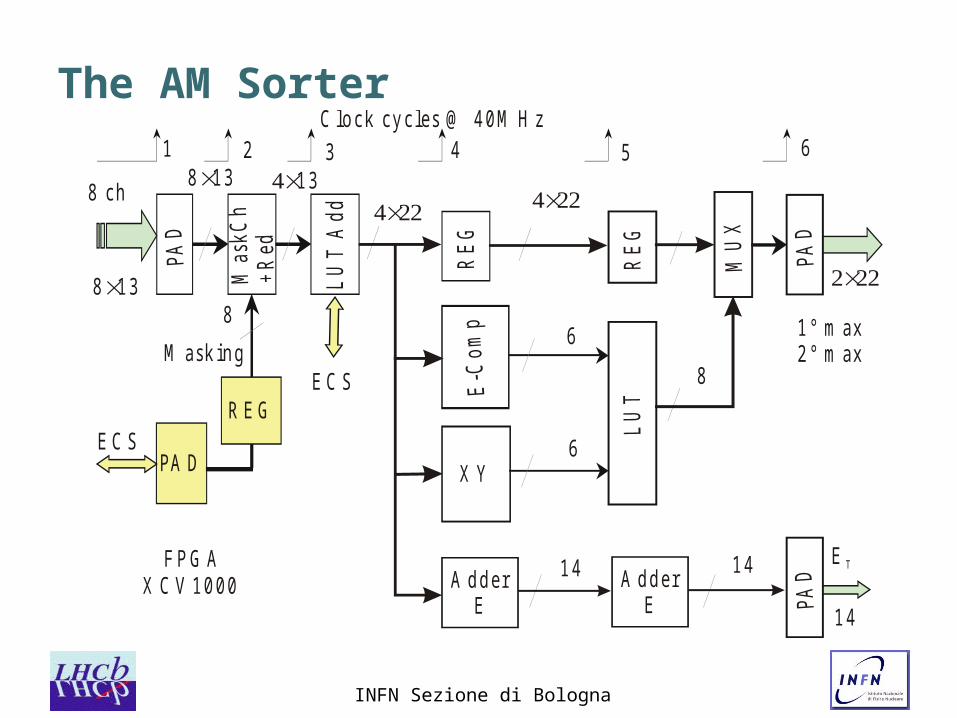
The AM Sorter
PAD
LU
T A
dd
8 1 3 1 3
PAD
8 1 3
8 ch
PAD
RE
G
RE
G
MU
X
M ask in g
8
R E G
PA D
A d d e r E
A d d e r E
1 4 1 4
1 4
E T
E C S
E C S
F P G AX C V 1 0 0 0
1 2 3 4 5 6
Mas
kCh
+R
ed
C lo ck cy c le s @ 4 0 M H z
1 ° m ax2 ° m ax
6
LU
T
8
X Y6
E-C
omp

INFN Sezione di Bologna
Sorter Logic
VME InterfaceProcessor Logic
FPGA
ECS
Interface
Optical Interface
Auxiliary
Electronics
LVDS
Parallel
INFN Sezione di Bologna
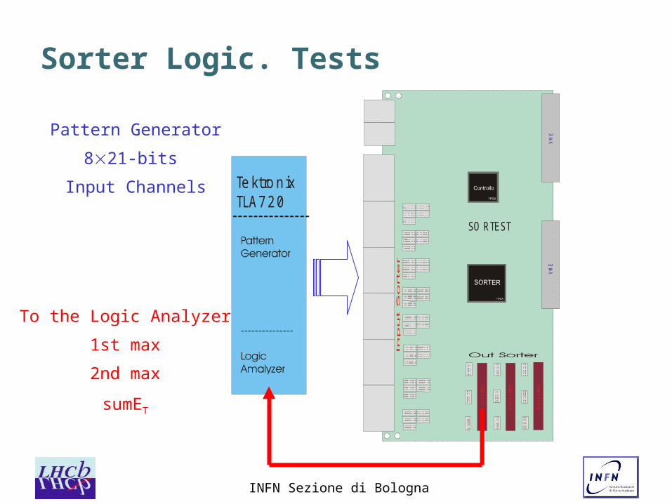
Sorter Logic. Tests
Out
Sor
ter
VM
EV
ME
Ou
t Sor
ter
Ou
t Sor
ter
SO RTEST
Te ktro nixTLA720
---------------
Pattern Generator
821-bits
Input Channels
To the Logic Analyzer
1st max
2nd max
sumET
INFN Sezione di Bologna
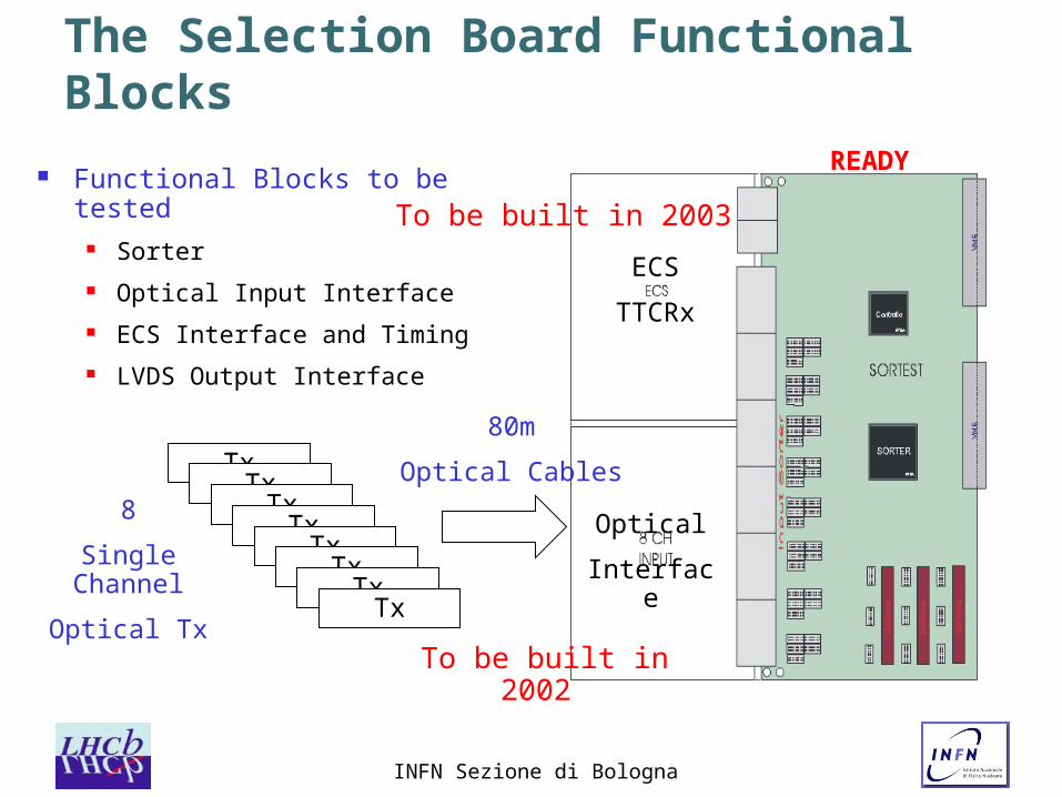
The Selection Board Functional Blocks
Functional Blocks to be tested
Sorter Optical Input Interface ECS Interface and Timing LVDS Output Interface
8
Single Channel
Optical Tx
TxTx
TxTx
TxTx
TxTx
To be built in 2002
To be built in 2003
80m
Optical Cables
READY
ECS
TTCRx
Optical
Interface