The influence of surface preparation on low temperature...
9
The influence of surface preparation on low temperature HfO2 ALD on InGaAs (001) and (110) surfaces Tyler Kent, Kechao Tang, Varistha Chobpattana, Muhammad Adi Negara, Mary Edmonds, William Mitchell, Bhagawan Sahu, Rohit Galatage, Ravi Droopad, Paul McIntyre, and Andrew C. Kummel Citation: The Journal of Chemical Physics 143, 164711 (2015); doi: 10.1063/1.4934656 View online: http://dx.doi.org/10.1063/1.4934656 View Table of Contents: http://scitation.aip.org/content/aip/journal/jcp/143/16?ver=pdfcov Published by the AIP Publishing Articles you may be interested in Effect of atomic layer deposition growth temperature on the interfacial characteristics of HfO2/p-GaAs metal- oxide-semiconductor capacitors J. Appl. Phys. 116, 222207 (2014); 10.1063/1.4902963 Surface and interfacial reaction study of half cycle atomic layer deposited HfO2 on chemically treated GaSb surfaces Appl. Phys. Lett. 102, 131602 (2013); 10.1063/1.4800441 Impact of atomic layer deposition temperature on HfO2/InGaAs metal-oxide-semiconductor interface properties J. Appl. Phys. 112, 084103 (2012); 10.1063/1.4759329 Realization of high-quality HfO2 on In0.53Ga0.47As by in-situ atomic-layer-deposition Appl. Phys. Lett. 100, 172110 (2012); 10.1063/1.4706261 Electrical characteristics of metal-oxide-semiconductor capacitors on p -GaAs using atomic layer deposition of ultrathin HfAlO gate dielectric Appl. Phys. Lett. 93, 193504 (2008); 10.1063/1.3007978 This article is copyrighted as indicated in the article. Reuse of AIP content is subject to the terms at: http://scitation.aip.org/termsconditions. Downloaded to IP: 137.110.60.78 On: Fri, 18 Dec 2015 18:27:18
Transcript of The influence of surface preparation on low temperature...

The influence of surface preparation on low temperature HfO2 ALD on InGaAs (001)and (110) surfacesTyler Kent, Kechao Tang, Varistha Chobpattana, Muhammad Adi Negara, Mary Edmonds, William Mitchell,Bhagawan Sahu, Rohit Galatage, Ravi Droopad, Paul McIntyre, and Andrew C. Kummel Citation: The Journal of Chemical Physics 143, 164711 (2015); doi: 10.1063/1.4934656 View online: http://dx.doi.org/10.1063/1.4934656 View Table of Contents: http://scitation.aip.org/content/aip/journal/jcp/143/16?ver=pdfcov Published by the AIP Publishing Articles you may be interested in Effect of atomic layer deposition growth temperature on the interfacial characteristics of HfO2/p-GaAs metal-oxide-semiconductor capacitors J. Appl. Phys. 116, 222207 (2014); 10.1063/1.4902963 Surface and interfacial reaction study of half cycle atomic layer deposited HfO2 on chemically treated GaSbsurfaces Appl. Phys. Lett. 102, 131602 (2013); 10.1063/1.4800441 Impact of atomic layer deposition temperature on HfO2/InGaAs metal-oxide-semiconductor interfaceproperties J. Appl. Phys. 112, 084103 (2012); 10.1063/1.4759329 Realization of high-quality HfO2 on In0.53Ga0.47As by in-situ atomic-layer-deposition Appl. Phys. Lett. 100, 172110 (2012); 10.1063/1.4706261 Electrical characteristics of metal-oxide-semiconductor capacitors on p -GaAs using atomic layer depositionof ultrathin HfAlO gate dielectric Appl. Phys. Lett. 93, 193504 (2008); 10.1063/1.3007978
This article is copyrighted as indicated in the article. Reuse of AIP content is subject to the terms at: http://scitation.aip.org/termsconditions. Downloaded to IP:
137.110.60.78 On: Fri, 18 Dec 2015 18:27:18

THE JOURNAL OF CHEMICAL PHYSICS 143, 164711 (2015)
The influence of surface preparation on low temperature HfO2 ALDon InGaAs (001) and (110) surfaces
Tyler Kent,1 Kechao Tang,2 Varistha Chobpattana,3 Muhammad Adi Negara,2Mary Edmonds,1 William Mitchell,3 Bhagawan Sahu,4 Rohit Galatage,4 Ravi Droopad,5Paul McIntyre,2 and Andrew C. Kummel11Materials Science and Engineering Department, University of California, San Diego, California 9500, USA2Materials Science and Engineering Department, Stanford University, Stanford, California 94305, USA3Materials Department, University of California, Santa Barbara, California 93106, USA4Global Foundries, 2600 Great America Way, Santa Clara, California 95054, USA5Department of Physics, Texas State University, San Marcos, Texas 78666, USA
(Received 16 July 2015; accepted 13 October 2015; published online 29 October 2015)
Current logic devices rely on 3D architectures, such as the tri-gate field effect transistor (finFET),which utilize the (001) and (110) crystal faces simultaneously thus requiring passivation methods forthe (110) face in order to ensure a pristine 3D surface prior to further processing. Scanning tunnelingmicroscopy (STM), x-ray photoelectron spectroscopy (XPS), and correlated electrical measurementon MOSCAPs were utilized to compare the effects of a previously developed in situ pre-atomiclayer deposition (ALD) surface clean on the InGaAs (001) and (110) surfaces. Ex situ wet cleansare very effective on the (001) surface but not the (110) surface. Capacitance voltage indicated the(001) surface with no buffered oxide etch had a higher Cmax hypothesized to be a result of poornucleation of HfO2 on the native oxide. An in situ pre-ALD surface clean employing both atomic Hand trimethylaluminum (TMA) pre-pulsing, developed by Chobpattana et al. and Carter et al. for the(001) surface, was demonstrated to be effective on the (110) surface for producing low Dit high CoxMOSCAPs. Including TMA in the pre-ALD surface clean resulted in reduction of the magnitudeof the interface state capacitance. The XPS studies show the role of atomic H pre-pulsing is toremove both carbon and oxygen while STM shows the role of TMA pre-pulsing is to eliminate Hinduced etching. Devices fabricated at 120 ◦C and 300 ◦C were compared. C 2015 AIP PublishingLLC. [http://dx.doi.org/10.1063/1.4934656]
INTRODUCTION
A few of the major obstacles facing III-V based transistorsis the increased power dissipation that results from subthresh-old leakage current, band to band tunneling, and aggressivegate oxide scaling.1,2 Tunneling through the gate oxide exhibitsan exponential dependence on oxide thickness, and scalingdielectric below 1 nm equivalent oxide thickness (EOT) resultsin unacceptable leakage currents.3,4 In order to minimize gateleakage, without sacrificing capacitance, high-k materials canbe employed. This allows for a physically thicker oxide andequal or higher capacitances than for traditional SiO2 dielec-trics.5–8 Utilizing high-k materials such as HfO2 and Al2O3 hasalready allowed for EOT below 1 nm and devices that out-perform traditional Si based metal oxide semiconductor fieldeffect transistors (MOSFETs).9,10 This work focuses on depo-sition of high-k on III-V channels; to continue aggressivelyscaling the gate oxide on III-V’s it is crucial to maximize thenucleation density of the high-k atomic layer deposition (ALD)precursors so that the dielectric film closes to form a contin-uous film on the substrate in a small number of ALD cycles.
Compound semiconductor based MOS devices also sufferfrom a relatively high density of interface trap states (Dit) at thesemiconductor/high-k interface. These electronic trap statesresult from physical defects at the interface such as dangling
bonds, metallic bonds, strained bonds, and defective nativeoxides. These can result directly from poor initiation of high-kALD on the semiconductor surface.11–13 To increase drivecurrent and minimize power consumption of III-V devices, it isimportant to minimize the Dit. Subcutaneous oxidation of thesubstrate and plasma induced damage during pre-ALD surfacecleans can also generate Dit. It is possible to utilize hydrogento remove native oxide as demonstrated by Melitz et al.14
and Carter et al.,15 and Chobpattana et al.,16 demonstratedthat by utilizing trimethylaluminum (TMA) and H2 plasmaprior to ALD of Al2O3 and HfO2 capacitance voltage (CV)characteristics can be improved at 300 ◦C.17
In this study, a pre-ALD ex situ wet clean and in situdry etch were examined on both InGaAs (001) and InGaAs(110) surfaces in order to determine their effects on the nucle-ation of HfO2 during ALD at 120 ◦C. The different surfacereconstructions result not only in different Fermi level pinningbehavior but also in varying degrees of nucleation for HfO2and thus interface trap density. In the absence of TMA inthe process, low ALD temperature is of interest in order tominimize hydrogen plasma damage of both the (001) and (110)surfaces and to limit subcutaneous oxidation of the substrateby H2O and O2, both of which can diffuse through HfO2.18
Scanning tunneling microscopy was used to gain an atomiclevel understanding of the processes occurring during the
0021-9606/2015/143(16)/164711/8/$30.00 143, 164711-1 © 2015 AIP Publishing LLC
This article is copyrighted as indicated in the article. Reuse of AIP content is subject to the terms at: http://scitation.aip.org/termsconditions. Downloaded to IP:
137.110.60.78 On: Fri, 18 Dec 2015 18:27:18

164711-2 Kent et al. J. Chem. Phys. 143, 164711 (2015)
in situ clean. X-ray photoelectron spectroscopy (XPS) and CVanalysis were used to determine the effect of a buffered oxideetch (BOE) on the nucleation of HfO2.
EXPERIMENTAL
MOSCAPs were fabricated with 300 nm of InGaAs (001)grown by molecular beam epitaxy (MBE) with 1 × 1017 cm−3
Si doping on n-type InP (001) substrates. The InGaAs (110)samples were grown by MBE with 1 × 1017 cm−3 Si dopingon InP (110) substrates. MOSCAP samples were initially de-greased for 3 min in acetone, isopropyl alcohol (IPA), anddeionized (DI) water. Immediately prior to loading samplesinto the ALD chamber, for some samples, the native oxide wasremoved with a 3 min dip in a BOE solution comprised ofa 30:4 ratio of 36% NH4F and 8% HF followed by a 1 minrinse in DI water. Samples were quickly loaded (1-2 min airexposure) into an Oxford Instruments FlexAL ALD reactorequipped with a remote plasma source which enables lowtemperature ALD and minimizes surface damage. Some sam-ples received an in situ surface clean prior to ALD consisting ofa 20 mTorr inductively coupled 100 W H2 plasma for 2 s, 40 msof 200 mTorr TMA, and another H2 plasma pulse. For someexperiments, the TMA pulse was eliminated.15,16 For samplesdeposited with HfO2 at 120 ◦C, an ALD cycle consisted ofa 1 s pulse of 80 mTorr tetrakis(ethylmethylamino)hafnium(TEMAH), a 7 s Ar purge, a 1 s 80 mTorr H2O pulse, anda 35 s purge. For samples deposited with HfO2 at 300 ◦Ca 1 s 80 mTorr pulse of TEMAH, 5 s Ar purge, 5 s pump,0.05 s 80 mTorr H2O pulse 7 s Ar purge, and 7 s pump wereemployed. All samples underwent a 15 min 400 ◦C forminggas anneal (FGA, 5% H2, 95% N2) prior to metal deposi-tion. The gate metal was 50 nm thick thermally evaporatedNi deposited in 150 µm diameter circular electrodes using ashadow mask. Thermal evaporation was utilized since previouswork has shown ebeam evaporation can increase Dit. The back-side contact was a blanket deposited 20 nm thick thermallyevaporated Ni film coated by 80 nm of thermally evaporatedAu. CV, IV curves were measured using a HP4284A LCRmeter and an Agilent B1500 Semiconductor Device Analyzer.The frequency range of all CV measurements is from 1 kHz(blue) to 1 MHz (grey). All Dit values were calculated usingthe full interface state model.19 At least 10 CV measurementswere performed on separate gates for each sample to ensureuniformity across the sample.
InGaAs (001) samples used for scanning tunneling micro-scopy (STM) were grown by MBE with 1 × 1018 cm−3 Sidoping on InP (001) substrates and were capped with 50 nm ofAs2. Samples were loaded into a variable temperature Omicronultrahigh vacuum chamber and the As2 cap was removed byheating the samples to 350 ◦C for 30 min and the (2 × 4) recon-struction was obtained by heating to 400 ◦C for at least 30 min.Details of the (2 × 4) reconstruction are given elsewhere.20,21
Samples were subsequently exposed to atomic H generatedfrom an Oxford Applied Research TC-50 thermal gas cracker.The hydrogen doses are reported in Langmuir (1 L = 1 s at1 × 10−6 Torr) based on the H2 pressure; however, the crackingefficiency is reported to be closer to 50% (Oxford Applied Re-search) but could not be verified; therefore, the reported atomic
H doses are an upper limit. Various amounts of TMA werealso deposited on the samples; details of specific dose amountsof atomic H and TMA are given in the section titled “Resultsand Discussion.” After dosing, samples were transferred tothe scanning probe microscopy (SPM) chamber, base pressure∼1 × 10⁻¹¹ Torr. STM was performed using a tunneling currentset point of 100 pA and a constant tip-sample bias of −3.0 V.All STM images were reproduced at least twice. XPS was per-formed with a monochromatic XM 1000 MkII/Sphera systemdeveloped by Omicron Nanotechnology. A constant analyzerpass energy of 50 eV was employed with a 0.1 eV linewidth ob-tained using a monochromatic Al Kα source (1486.7 eV). Thetakeoff angle was 30◦ relative to the surface (surface sensitive)with an acceptance angle of 7◦. All spectra were analyzed withCASA XPS v. 2.3. An assumption made in this study is that themajority of reactive species created in the plasma are atomicH and thus using a thermal atomic H source for XPS and STMstudies is a valid comparison. The thermally generated atomicH was at 1 × 10⁻⁶ Torr while the H plasma was at 0.02 Torrso plasma induced damaged in CV due to atomic H wouldbe, if anything, lower than the damage you would expect fromthermally generated atomic H.
RESULTS AND DISCUSSION
In situ native oxide/contaminant removal
Capacitance voltage profiling is an effective way to bothqualitatively determine the quality of the oxide and quantita-tively determine the trap density at the semiconductor/oxideinterface (Dit) and the border trap density in the oxide (Nbt).For n-type samples at positive gate biases >1 V, electrons accu-mulate at the surface of the InGaAs and the measured capaci-tance is a reflection of the thickness and quality of the oxide.
The dispersion with frequency upon sweeping the gatebias toward accumulation reflects the density of border traps(Nbt) in the absence of series (e.g., contact) resistance. Theborder trap response is frequency dependent because the timeconstant for filling and emptying the traps depends on theirdepth and energy distributions in the oxide. The magnitude ofthe accumulation dispersion with frequency gives a qualitativedescription of the Nbt and, when more thorough modelingtechniques are used, this dispersion can contribute to the quan-tification of Nbt.
As the gate bias is swept toward inversion, a “false inver-sion bump” is frequently observed for III-V substrates. Thisis a result of charges being injected into electronic trap statesat the interface (Dit), rather than true inversion. When sweepingthe bias outside of the energy range of the traps, or whenthe measurement frequency and/or temperature is too low todetect the capacitive signature of the traps, this trap capacitancesubsides. The magnitude of the false inversion bump givesa qualitative description of the Dit and, when more thoroughmodeling techniques are used, this bump can contribute tothe quantification of Dit.
The effect of TMA incorporation into the in situ pre-ALDsurface clean was investigated by fabricating MOSCAPs onInGaAs (001) with 10 cycles of either H plasma alone orH/TMA/H followed by 40 cycles of HfO2 ALD at 120 ◦C or
This article is copyrighted as indicated in the article. Reuse of AIP content is subject to the terms at: http://scitation.aip.org/termsconditions. Downloaded to IP:
137.110.60.78 On: Fri, 18 Dec 2015 18:27:18
164711-3 Kent et al. J. Chem. Phys. 143, 164711 (2015)
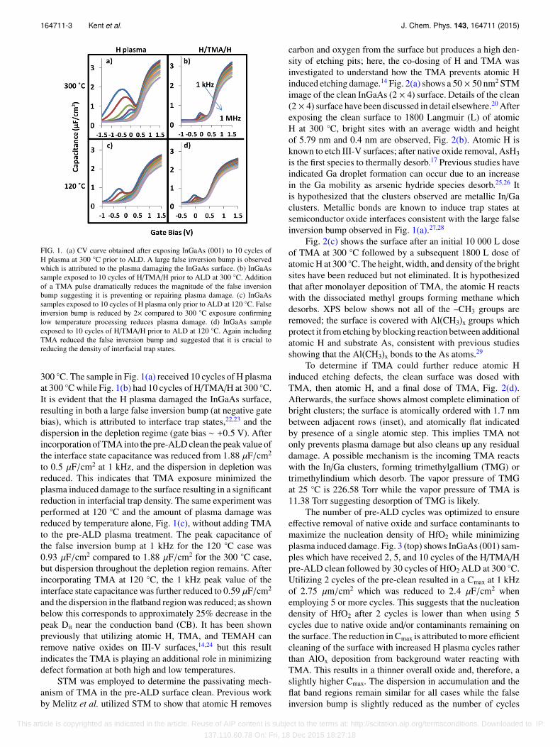
FIG. 1. (a) CV curve obtained after exposing InGaAs (001) to 10 cycles ofH plasma at 300 ◦C prior to ALD. A large false inversion bump is observedwhich is attributed to the plasma damaging the InGaAs surface. (b) InGaAssample exposed to 10 cycles of H/TMA/H prior to ALD at 300 ◦C. Additionof a TMA pulse dramatically reduces the magnitude of the false inversionbump suggesting it is preventing or repairing plasma damage. (c) InGaAssamples exposed to 10 cycles of H plasma only prior to ALD at 120 ◦C. Falseinversion bump is reduced by 2× compared to 300 ◦C exposure confirminglow temperature processing reduces plasma damage. (d) InGaAs sampleexposed to 10 cycles of H/TMA/H prior to ALD at 120 ◦C. Again includingTMA reduced the false inversion bump and suggested that it is crucial toreducing the density of interfacial trap states.
300 ◦C. The sample in Fig. 1(a) received 10 cycles of H plasmaat 300 ◦C while Fig. 1(b) had 10 cycles of H/TMA/H at 300 ◦C.It is evident that the H plasma damaged the InGaAs surface,resulting in both a large false inversion bump (at negative gatebias), which is attributed to interface trap states,22,23 and thedispersion in the depletion regime (gate bias ∼ +0.5 V). Afterincorporation of TMA into the pre-ALD clean the peak value ofthe interface state capacitance was reduced from 1.88 µF/cm2
to 0.5 µF/cm2 at 1 kHz, and the dispersion in depletion wasreduced. This indicates that TMA exposure minimized theplasma induced damage to the surface resulting in a significantreduction in interfacial trap density. The same experiment wasperformed at 120 ◦C and the amount of plasma damage wasreduced by temperature alone, Fig. 1(c), without adding TMAto the pre-ALD plasma treatment. The peak capacitance ofthe false inversion bump at 1 kHz for the 120 ◦C case was0.93 µF/cm2 compared to 1.88 µF/cm2 for the 300 ◦C case,but dispersion throughout the depletion region remains. Afterincorporating TMA at 120 ◦C, the 1 kHz peak value of theinterface state capacitance was further reduced to 0.59 µF/cm2
and the dispersion in the flatband region was reduced; as shownbelow this corresponds to approximately 25% decrease in thepeak Dit near the conduction band (CB). It has been shownpreviously that utilizing atomic H, TMA, and TEMAH canremove native oxides on III-V surfaces,14,24 but this resultindicates the TMA is playing an additional role in minimizingdefect formation at both high and low temperatures.
STM was employed to determine the passivating mech-anism of TMA in the pre-ALD surface clean. Previous workby Melitz et al. utilized STM to show that atomic H removes
carbon and oxygen from the surface but produces a high den-sity of etching pits; here, the co-dosing of H and TMA wasinvestigated to understand how the TMA prevents atomic Hinduced etching damage.14 Fig. 2(a) shows a 50 × 50 nm2 STMimage of the clean InGaAs (2 × 4) surface. Details of the clean(2 × 4) surface have been discussed in detail elsewhere.20 Afterexposing the clean surface to 1800 Langmuir (L) of atomicH at 300 ◦C, bright sites with an average width and heightof 5.79 nm and 0.4 nm are observed, Fig. 2(b). Atomic H isknown to etch III-V surfaces; after native oxide removal, AsH3is the first species to thermally desorb.17 Previous studies haveindicated Ga droplet formation can occur due to an increasein the Ga mobility as arsenic hydride species desorb.25,26 Itis hypothesized that the clusters observed are metallic In/Gaclusters. Metallic bonds are known to induce trap states atsemiconductor oxide interfaces consistent with the large falseinversion bump observed in Fig. 1(a).27,28
Fig. 2(c) shows the surface after an initial 10 000 L doseof TMA at 300 ◦C followed by a subsequent 1800 L dose ofatomic H at 300 ◦C. The height, width, and density of the brightsites have been reduced but not eliminated. It is hypothesizedthat after monolayer deposition of TMA, the atomic H reactswith the dissociated methyl groups forming methane whichdesorbs. XPS below shows not all of the –CH3 groups areremoved; the surface is covered with Al(CH3)x groups whichprotect it from etching by blocking reaction between additionalatomic H and substrate As, consistent with previous studiesshowing that the Al(CH3)x bonds to the As atoms.29
To determine if TMA could further reduce atomic Hinduced etching defects, the clean surface was dosed withTMA, then atomic H, and a final dose of TMA, Fig. 2(d).Afterwards, the surface shows almost complete elimination ofbright clusters; the surface is atomically ordered with 1.7 nmbetween adjacent rows (inset), and atomically flat indicatedby presence of a single atomic step. This implies TMA notonly prevents plasma damage but also cleans up any residualdamage. A possible mechanism is the incoming TMA reactswith the In/Ga clusters, forming trimethylgallium (TMG) ortrimethylindium which desorb. The vapor pressure of TMGat 25 ◦C is 226.58 Torr while the vapor pressure of TMA is11.38 Torr suggesting desorption of TMG is likely.
The number of pre-ALD cycles was optimized to ensureeffective removal of native oxide and surface contaminants tomaximize the nucleation density of HfO2 while minimizingplasma induced damage. Fig. 3 (top) shows InGaAs (001) sam-ples which have received 2, 5, and 10 cycles of the H/TMA/Hpre-ALD clean followed by 30 cycles of HfO2 ALD at 300 ◦C.Utilizing 2 cycles of the pre-clean resulted in a Cmax at 1 kHzof 2.75 µm/cm2 which was reduced to 2.4 µF/cm2 whenemploying 5 or more cycles. This suggests that the nucleationdensity of HfO2 after 2 cycles is lower than when using 5cycles due to native oxide and/or contaminants remaining onthe surface. The reduction in Cmax is attributed to more efficientcleaning of the surface with increased H plasma cycles ratherthan AlOx deposition from background water reacting withTMA. This results in a thinner overall oxide and, therefore, aslightly higher Cmax. The dispersion in accumulation and theflat band regions remain similar for all cases while the falseinversion bump is slightly reduced as the number of cycles
This article is copyrighted as indicated in the article. Reuse of AIP content is subject to the terms at: http://scitation.aip.org/termsconditions. Downloaded to IP:
137.110.60.78 On: Fri, 18 Dec 2015 18:27:18

164711-4 Kent et al. J. Chem. Phys. 143, 164711 (2015)
FIG. 2. (a) Clean InGaAs (2×4) sur-face. (b) (2×4) surface after exposureto atomic H at 300 ◦C. Formation ofbright white clusters is observed withan average width of 5.79 nm and aver-age height of 0.4 nm. (c) (2×4) surfaceinitially exposed to TMA and subse-quently atomic H, both at 300 ◦C. Den-sity, height, and width of bright siteshave been reduced. TMA may be pro-viding alternate reaction pathways forthe atomic H, such as formation anddesorption of methane. (d) (2×4) sur-face exposed first to TMA, then atomicH, and a final dose of TMA. The whiteclusters are almost completely absentand the surface maintains atomic order-ing (inset) and is atomically flat. Thissuggests TMA both prevents plasmadamage as well as cleans up the remain-ing damage observed in (c). The TMAmay react with the clusters and formvolatile by products.
increases. The weak inversion frequency response of MOScapacitors is increasingly sensitive to Dit as the Cmax value,indicative of the oxide capacitance, decreases.30 Therefore, thesmaller interface trap bumps in the inversion region seen in
Fig. 3 for increasing numbers of H/TMA/H cleaning cycles areconsistent with removal of defect-inducing adsorbates on theInGaAs surface that create interfacial trap states. Additionally,despite a 5× increase in H plasma exposure, no damage is
FIG. 3. (Top row) The number of pre-ALD H/TMA/H cycles was varied at 300 ◦C. Exposing the sample to 5 or more cycles of the pre clean results in a Cmax of∼2.4 µF/cm2. This reduction in Cmax compared to the 2 cycle case is attributed to an increase in nucleation density of HfO2 which results from more efficientremoval of native oxide or surface contaminants with 5 or more cycles. At 120 ◦C (bottom row), the Cmax continually decreases as the number of cleaning cyclesincreases. This suggests that the H plasma is not effective at removing native oxide at lower temperatures; hence, more cleaning cycles are required to maximizethe nucleation density of HfO2. It is important to note that despite a 5× increase in plasma exposure at both temperatures, the false inversion bump actuallydecreases indicating efficient surface cleaning by the H plasma and also the importance of TMA in protecting the surface from plasma damage.
This article is copyrighted as indicated in the article. Reuse of AIP content is subject to the terms at: http://scitation.aip.org/termsconditions. Downloaded to IP:
137.110.60.78 On: Fri, 18 Dec 2015 18:27:18

164711-5 Kent et al. J. Chem. Phys. 143, 164711 (2015)
evident in the CV profile, emphasizing the protective role ofTMA in the pre-ALD clean.
Performing the same experiments at 120 ◦C, Fig. 3(bottom) indicates that, at lower temperatures, at least 10H/TMA/H cycles are required to maximize the effectivenessof the plasma treatment and enhance the nucleation of HfO2during subsequent ALD. The Cmax value continually decreasesas the number of pre-ALD cycles increases, suggesting itis more difficult to remove oxide or contamination at lowtemperatures. The frequency dispersion of capacitance inaccumulation and depletion shows no significant changeamong the samples, but the Dit bump in the inversion regiondoes decrease with increasing number of cycles, as for the300 ◦C ALD condition. Again, despite a 5× increase in plasmaexposure, we see no evidence of plasma damage, highlightingthe importance of TMA in this process. When 20 cycles areemployed there is noticeable plasma damage (not shown).
Ex situ native oxide removal
Wet BOEs are routinely used to remove oxide from III-Vsubstrates prior to processing. The effect of the BOE on both(001) and (110) surfaces and its impact on HfO2 nucleation at120 ◦C and 300 ◦C were studied. Fig. 4 compares (001) and(110) samples which received a BOE (left column) and didnot receive a BOE (right column) at 120 ◦C. The wet cleanedsamples were loaded into the ALD reactor with a maximum2 min air exposure. All four samples were in the ALD reactorsimultaneously to ensure identical deposition conditions, andeach received 10 cycles of H/TMA/H pre-ALD surface cleanand 30 cycles of HfO2 ALD. The (001) sample which receivedthe BOE shows a maximum capacitance at high frequency of
FIG. 4. InGaAs (001) samples which did (top left) and did not (top right)receive a BOE immediately prior to ALD at 120 ◦C. (001) sample which didnot receive a BOE shows a Cmax of about 2.6 µF/cm2 compared to 2 µF/cm2
for the no BOE sample. It is hypothesized that the HfO2 nucleates more effi-ciently on the sample which was exposed to the BOE. All four samples werein the ALD reactor simultaneously to ensure identical deposition conditions.(110) samples that did (bottom left) and did not receive (bottom right) a BOEprior to ALD show nearly identical CV spectra. This suggests that the BOE isnot effective on the (110) surface and emphasizes the need for an in situ dryetch which can clean both surfaces effectively.
∼2 µF/cm2, whereas the sample which did not receive theBOE shows a Cmax of ∼2.6 µF/cm2. It is hypothesized thatthe native oxide on the non-BOE sample limits the nucleationof HfO2 on the (001) surface. Limited nucleation would resultin a thinner overall oxide and, therefore, a higher Cmax. Ad-ditionally, the non-BOE sample shows a slightly Dit bump ininversion. This can be attributed to the presence of a variety ofInGaAs native oxides which are known to be a source of trapstates in III-V based devices.11,31,32 The (110) surface showsno significant difference between the wet cleaned and non-wetcleaned samples. This indicates HfO2 is nucleating identicallyon both samples, suggesting the BOE is not effective on thissurface or that the (110) surface has such a thin native oxidethat the BOE etch is immaterial when in situ atomic H isemployed, consistent with the XPS data described later in thisreport.
The same experiment was performed at 300 ◦C exceptthe samples received 48 cycles of HfO2 ALD to account fora lower growth rate, Fig. 5. Similar behavior was observed forthe (001) InGaAs samples. The Cmax for the non-BOE samplewas 2.8 µF/cm2 compared to ∼2.4 µF/cm2 for the samplewhich received a BOE. It is hypothesized that the HfO2 is notnucleating as efficiently on the sample with a thicker nativeoxide, resulting in a thinner HfO2 layer. The interface trapresponses in the inversion region of the associated MOSCAPsare comparable, which can be attributed to the increased effec-tiveness of the H plasma at 300 ◦C. For the (110) samples,the Cmax of the sample which did not receive a BOE is within10% of the Cmax of the BOE sample, and thus not material.The leakage current densities of the 300 ◦C samples weremuch higher than the 120 ◦C samples.33 For example, the120 ◦C InGaAs (001) and InGaAs (110) samples had about100× lower leakage current density at +1 V relative to the
FIG. 5. InGaAs (001) samples which did (top left) and did not (top right) re-ceive a BOE immediately prior to ALD at 300 ◦C. (001) sample which did notreceive a BOE shows a Cmax of about 2.8 µF/cm2 compared to 2.4 µF/cm2
for the no BOE sample. It is hypothesized that the HfO2 nucleates moreefficiently on the sample which was exposed to the BOE. All 4 samples werein the ALD reactor simultaneously to ensure identical deposition conditions.The (110) sample which did not receive a BOE shows a Cmax within 10% ofthe BOE sample hence any differences are immaterial.
This article is copyrighted as indicated in the article. Reuse of AIP content is subject to the terms at: http://scitation.aip.org/termsconditions. Downloaded to IP:
137.110.60.78 On: Fri, 18 Dec 2015 18:27:18
164711-6 Kent et al. J. Chem. Phys. 143, 164711 (2015)
flat band voltage (Vfb) than the corresponding 300 ◦C samples.This may be due to the presence of a small CVD componentin the 120 ◦C ALD recipe which resulted in thicker oxides. At120 ◦C, the growth rate per cycles was ∼1.4 Å/cycle while at300 ◦C the growth rate was closer to 1 Å/cycles, as measuredby ellipsometry.
X-ray photoelectron spectroscopy
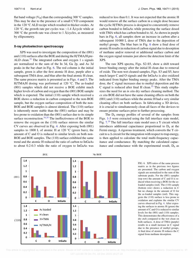
XPS was used to investigate the composition of the (001)and (110) surfaces after the BOE and during the H/TMA/H pre-ALD clean.33 The integrated carbon and oxygen 1 s signalsare normalized to the sum of the In 3d, Ga 2p, and As 3dpeaks in the bar chart in Fig. 6. The red column is the initialsample, green is after the first atomic H dose, purple after asubsequent TMA dose, and blue after the final atomic H clean.The same process matrix is presented as in Figs. 4 and 5. TheH/TMA/H dosing was performed at 120 ◦C. The as-loaded(001) samples which did not receive a BOE exhibit muchhigher levels of carbon and oxygen than the (001) BOE samplewhich is expected. The initial (110) sample which received aBOE shows a reduction in carbon compared to the non-BOEsample, but the oxygen surface composition of both the non-BOE and BOE samples is almost identical. The (110) surfaceis inherently more stable than the (001) surface and may beless prone to oxidation than the (001) surface due to its simplesurface reconstruction.34,35 The ineffectiveness of the BOE toremove the oxygen on the (110) surface mirrors the similarCV curves are observed in Fig. 4. After exposing both (001)samples to 1800 L of atomic H at 120 ◦C (green bars), theamount of C and O is reduced to similar levels on both non-BOE and BOE samples. The (110) surface exhibited the sametrend and the atomic H reduced the ratio of carbon to InGaAsto about 0.2-0.3 while the ratio of oxygen to InGaAs was
reduced to less than 0.1. It was not expected that the atomic Hwould remove all the surface carbon in a single dose becausethe cyclic H/TMA process is designed to concurrently removecarbon bonded to InGaAs while protecting the surface dosedwith TMA which has carbon bonded to Al. As shown in purplebars in Fig. 6, all samples show an increase in carbon after asubsequent 10 000 L dose of TMA due to the deposition ofmethyl groups. The blue bars in Fig. 6 show a final dose ofatomic H results in reduction of carbon signal due to desorptionof methane and/or removal or additional surface carbon andthe oxygen signal remains just above the detection limit of theXPS.
The raw XPS spectra, Figs. S2-S5, show a shift towardlower binding energy after the initial H clean due to removalof oxide. The non-wet cleaned samples, Figs. S3 and S5, havemuch larger C and O signals and the InGaAs is also oxidizedindicated from higher binding energy peaks. After the TMAdose, the C signal increases due to methyl deposition and theC signal is reduced after final H clean.33 This study empha-sizes the need for an in situ dry surface cleaning method. Theex situ BOE did not have the same cleaning effects on both the(001) and (110) surfaces while the atomic H had a very similarcleaning effect on both surfaces. In fabricating a 3D device,it is crucial to simultaneously clean all faces of the devices toensure pristine surfaces prior to further processing.
The Dit energy profiles of several of the samples fromFigs. 1-5 were extracted using the full interface state model,Fig. 7.19 The full interface state model uses a Y circuit whichintroduces additional capacitance proportional to Dit at theFermi energy. A rigorous treatment, which converts the Y cir-cuit to a∆ circuit for the integration with respect to trap energy,is then applied to calculate the total multi-frequency capac-itance and conductance. By matching the calculated capac-itance and conductance with the experimental result, Dit as
FIG. 6. XPS ratios of the same processmatrix as in the previous two figuresare presented. The carbon and oxygensignals are normalized to the sum of thesubstrate peaks. For the (001) samples(top row) the amount of C and O is re-duced when receiving a BOE for the as-loaded samples (red). The (110) sample(bottom row) shows a reduction in Cbut no change in the amount of O forthe as-loaded samples (red). This sug-gests the (110) surface is less prone tooxidation and explains the similar CVcurves observed in Fig. 4. After expos-ing the surfaces to atomic H (green) theamount of C and O is reduced to similarlevels for the (001) and (110) samples.This demonstrates the effectiveness of adry etch compared to the wet clean onboth surfaces. A dose of TMA (purple)results in a small increase in C signaldue to the presence of methyl groups.A final dose of atomic H reduces the Csignal from methane desorption.
This article is copyrighted as indicated in the article. Reuse of AIP content is subject to the terms at: http://scitation.aip.org/termsconditions. Downloaded to IP:
137.110.60.78 On: Fri, 18 Dec 2015 18:27:18
164711-7 Kent et al. J. Chem. Phys. 143, 164711 (2015)
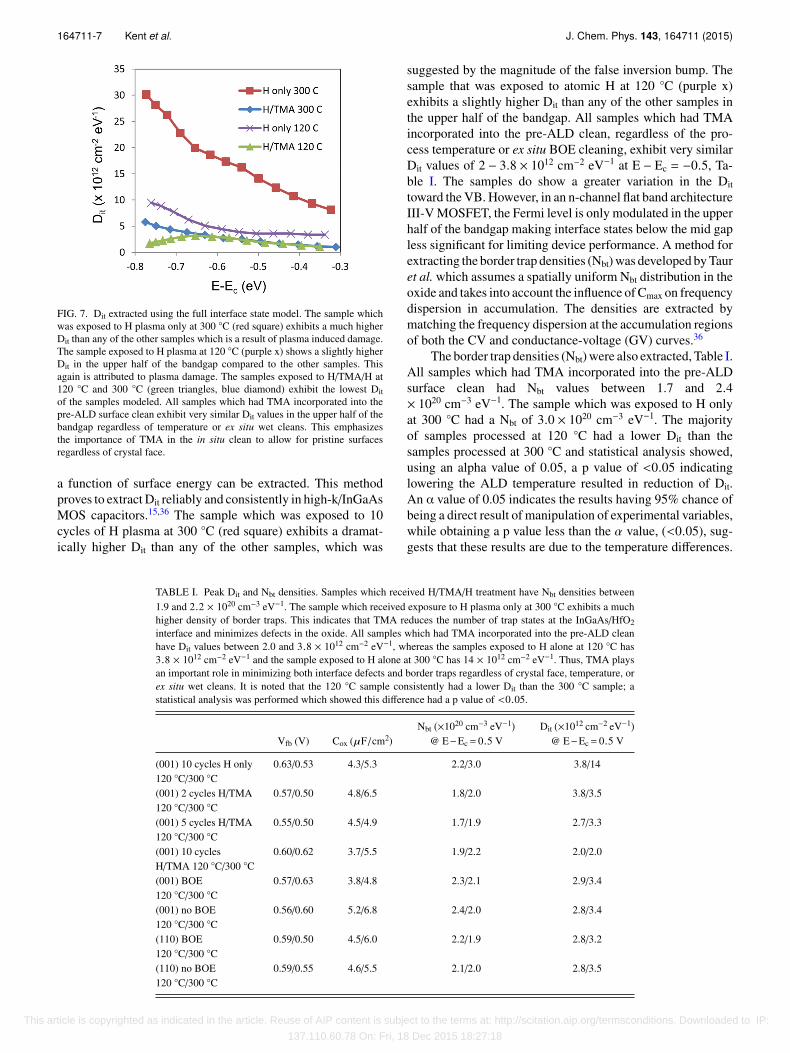
FIG. 7. Dit extracted using the full interface state model. The sample whichwas exposed to H plasma only at 300 ◦C (red square) exhibits a much higherDit than any of the other samples which is a result of plasma induced damage.The sample exposed to H plasma at 120 ◦C (purple x) shows a slightly higherDit in the upper half of the bandgap compared to the other samples. Thisagain is attributed to plasma damage. The samples exposed to H/TMA/H at120 ◦C and 300 ◦C (green triangles, blue diamond) exhibit the lowest Ditof the samples modeled. All samples which had TMA incorporated into thepre-ALD surface clean exhibit very similar Dit values in the upper half of thebandgap regardless of temperature or ex situ wet cleans. This emphasizesthe importance of TMA in the in situ clean to allow for pristine surfacesregardless of crystal face.
a function of surface energy can be extracted. This methodproves to extract Dit reliably and consistently in high-k/InGaAsMOS capacitors.15,36 The sample which was exposed to 10cycles of H plasma at 300 ◦C (red square) exhibits a dramat-ically higher Dit than any of the other samples, which was
suggested by the magnitude of the false inversion bump. Thesample that was exposed to atomic H at 120 ◦C (purple x)exhibits a slightly higher Dit than any of the other samples inthe upper half of the bandgap. All samples which had TMAincorporated into the pre-ALD clean, regardless of the pro-cess temperature or ex situ BOE cleaning, exhibit very similarDit values of 2 − 3.8 × 1012 cm−2 eV−1 at E − Ec = −0.5, Ta-ble I. The samples do show a greater variation in the Dittoward the VB. However, in an n-channel flat band architectureIII-V MOSFET, the Fermi level is only modulated in the upperhalf of the bandgap making interface states below the mid gapless significant for limiting device performance. A method forextracting the border trap densities (Nbt) was developed by Tauret al. which assumes a spatially uniform Nbt distribution in theoxide and takes into account the influence of Cmax on frequencydispersion in accumulation. The densities are extracted bymatching the frequency dispersion at the accumulation regionsof both the CV and conductance-voltage (GV) curves.36
The border trap densities (Nbt) were also extracted, Table I.All samples which had TMA incorporated into the pre-ALDsurface clean had Nbt values between 1.7 and 2.4× 1020 cm−3 eV−1. The sample which was exposed to H onlyat 300 ◦C had a Nbt of 3.0 × 1020 cm−3 eV−1. The majorityof samples processed at 120 ◦C had a lower Dit than thesamples processed at 300 ◦C and statistical analysis showed,using an alpha value of 0.05, a p value of <0.05 indicatinglowering the ALD temperature resulted in reduction of Dit.An α value of 0.05 indicates the results having 95% chance ofbeing a direct result of manipulation of experimental variables,while obtaining a p value less than the α value, (<0.05), sug-gests that these results are due to the temperature differences.
TABLE I. Peak Dit and Nbt densities. Samples which received H/TMA/H treatment have Nbt densities between1.9 and 2.2 × 1020 cm−3 eV−1. The sample which received exposure to H plasma only at 300 ◦C exhibits a muchhigher density of border traps. This indicates that TMA reduces the number of trap states at the InGaAs/HfO2interface and minimizes defects in the oxide. All samples which had TMA incorporated into the pre-ALD cleanhave Dit values between 2.0 and 3.8 × 1012 cm−2 eV−1, whereas the samples exposed to H alone at 120 ◦C has3.8 × 1012 cm−2 eV−1 and the sample exposed to H alone at 300 ◦C has 14 × 1012 cm−2 eV−1. Thus, TMA playsan important role in minimizing both interface defects and border traps regardless of crystal face, temperature, orex situ wet cleans. It is noted that the 120 ◦C sample consistently had a lower Dit than the 300 ◦C sample; astatistical analysis was performed which showed this difference had a p value of <0.05.
Vfb (V) Cox (µF/cm2)Nbt (×1020 cm−3 eV−1)
@ E−Ec= 0.5 VDit (×1012 cm−2 eV−1)
@ E−Ec= 0.5 V
(001) 10 cycles H only120 ◦C/300 ◦C
0.63/0.53 4.3/5.3 2.2/3.0 3.8/14
(001) 2 cycles H/TMA120 ◦C/300 ◦C
0.57/0.50 4.8/6.5 1.8/2.0 3.8/3.5
(001) 5 cycles H/TMA120 ◦C/300 ◦C
0.55/0.50 4.5/4.9 1.7/1.9 2.7/3.3
(001) 10 cyclesH/TMA 120 ◦C/300 ◦C
0.60/0.62 3.7/5.5 1.9/2.2 2.0/2.0
(001) BOE120 ◦C/300 ◦C
0.57/0.63 3.8/4.8 2.3/2.1 2.9/3.4
(001) no BOE120 ◦C/300 ◦C
0.56/0.60 5.2/6.8 2.4/2.0 2.8/3.4
(110) BOE120 ◦C/300 ◦C
0.59/0.50 4.5/6.0 2.2/1.9 2.8/3.2
(110) no BOE120 ◦C/300 ◦C
0.59/0.55 4.6/5.5 2.1/2.0 2.8/3.5
This article is copyrighted as indicated in the article. Reuse of AIP content is subject to the terms at: http://scitation.aip.org/termsconditions. Downloaded to IP:
137.110.60.78 On: Fri, 18 Dec 2015 18:27:18
164711-8 Kent et al. J. Chem. Phys. 143, 164711 (2015)
This indicates that TMA-based surface treatment not onlyreduces the density of defects at the InGaAs/HfO2 interfacebut also results in a more robust oxide, as border traps areassociated with defects within the oxide and are thought tobe located within about 1 nm from the semiconductor/oxideinterface.37 The oxide capacitances (Cox) at 120 ◦C and 300 ◦Cvary due to anomalies in the ALD growth rate which canqualitatively influence the apparent magnitude of Dit bump butthe quantitative Dit will not be influenced since Cox is factoredin when extracting the Dit. While it is possible that, under someprocessing conditions, thinner oxide may have higher Dit dueto defect generation in metallization, it has been reported thatDit can be nearly invariant with oxide thickness.38
Even though the lowest Dit values reported in this study are1-2 orders of magnitude greater than those typical of SiO2/Siinterfaces, the obtained values are low for high-k/InGaAs gatestacks, which typically display Dit values in the range of 1.0× 1012 cm−2 eV−1 to 1.0 × 1013 cm−2 eV−1.16,39,40 In addition,there are several potential pitfalls in Dit analysis of III-V MOSdevices, requiring application of methods, such as the fullinterface state model used in this report, that avoid unphys-ical Dit extraction and underestimation of the trap density19
that may affect other results described in the literature. Fi-nally, the interface defects densities observed for the studiedHfO2/InGaAs gate stacks are well within the useful range forpotential application in end-of-roadmap MOS devices. Due tothe very high Cox values (low EOT) that would pertain forsuch devices, the effect of Dit on flat band voltage shift andsubthreshold swing is greatly reduced,41 making HfO2/InGaAsa strong candidate for future MOS transistors.
CONCLUSION
In situ STM and XPS were employed to determine the roleof TMA in a pre-ALD surface clean developed by Carter et al.and Chobpattana et al. and to determine the effectiveness ofthis clean on the InGaAs (110) surface. By employing STM,XPS, and CV profiling, TMA was determined to prevent andclean up etch damage caused by the atomic H. Consistentwith the reduction of H induced etch damage, incorporatingTMA reduced the magnitude of interface trap states at both300 ◦C and 120 ◦C by minimizing and preventing the formationof In/Ga clusters. Lowering the temperature alone resulted inreduction of trap states, but not to the same extent as whenincluding TMA. An ex situ BOE was examined on both the In-GaAs (001) and (110) surfaces. The BOE efficiently removedboth carbon and oxygen on the (001) surface but only removedcarbon on the (110) surface. This emphasizes the need for anall dry pre-ALD surface clean when depositing material on 3Dstructures since this will allow for efficient nucleation of ALDprecursors on all crystal planes.
ACKNOWLEDGMENTS
The authors would like to acknowledge the Semicon-ductor Research Corporation and the National Science Foun-dation Grant No. ECCS-1125017 as funding sources.
1F. Hamzaoglu and M. R. Stan, in Proceedings of the 2002 InternationalSymposium on Low Power Electronics and Design (ACM, 2002), p. 60.
2T. N. Theis and P. M. Solomon, Proc. IEEE 98, 2005 (2010).3J. Maserjian, J. Vac. Sci. Technol. 11, 996 (1974).4S. Lo, D. Buchanan, Y. Taur, and W. Wang, IEEE Electron Device Lett. 18,209 (1997).
5L. Kang, B. H. Lee, W.-J. Qi, Y. Jeon, R. Nieh, S. Gopalan, K. Onishi, andJ. C. Lee, IEEE Electron Device Lett. 21, 181 (2000).
6S.-G. Lim et al., J. Appl. Phys. 91, 4500 (2002).7M. Houssa, High-K Gate Dielectrics (CRC Press, 2003).8E. Gusev et al., in International Electron Devices Meeting, 2001.IEDM’01. Technical Digest (IEEE, 2001), p. 20.1. 1.
9D.-H. Kim et al., in Electron Devices Meeting (IEDM), 2014 IEEEInternational (IEEE, 2014), p. 25.2. 1.
10L. Chu, C. Merckling, A. Alian, J. Dekoster, J. Kwo, M. Hong, M. Caymax,and M. Heyns, Appl. Phys. Lett. 99, 042908 (2011).
11P. D. Ye, J. Vac. Sci. Technol., A 26, 697 (2008).12W. Mönch, Semiconductor Surfaces and Interfaces (Springer, 2001).13J. Robertson, Appl. Phys. Lett. 94, 152104 (2009).14W. Melitz, J. Shen, T. Kent, A. C. Kummel, and R. Droopad, J. Appl. Phys.
110, 013713 (2011).15A. D. Carter, W. J. Mitchell, B. J. Thibeault, J. J. Law, and M. J. Rodwell,
Appl. Phys. Express 4, 091102 (2011).16V. Chobpattana, J. Son, J. J. M. Law, R. Engel-Herbert, C.-Y. Huang, and S.
Stemmer, Appl. Phys. Lett. 102, 022907 (2013).17F. S. Aguirre-Tostado, M. Milojevic, C. L. Hinkle, E. M. Vogel, R. M.
Wallace, S. McDonnell, and G. J. Hughes, Appl. Phys. Lett. 92, 171906(2008).
18C. Driemeier, E. Gusev, and I. Baumvol, Appl. Phys. Lett. 88, 201901 (2006).19H.-P. Chen, Y. Yuan, B. Yu, J. Ahn, P. C. McIntyre, P. Asheck, M. J. Rodwell,
and Y. Taur, IEEE Trans. Electron Devices 59, 2383 (2012).20J. Shen, D. L. Winn, W. Melitz, J. B. Clemens, and A. C. Kummel, ECS
Trans. 16, 463 (2008).21W. Melitz, T. Kent, A. C. Kummel, R. Droopad, M. Holland, and I. Thayne,
J. Chem. Phys. 136, 154706 (2012).22H.-C. Lin, W.-E. Wang, G. Brammertz, M. Meuris, and M. Heyns, Micro-
electron. Eng. 86, 1554 (2009).23R. Engel-Herbert, Y. Hwang, and S. Stemmer, J. Appl. Phys. 108, 124101
(2010).24C. Hinkle et al., Appl. Phys. Lett. 92, 071901 (2008).25O. M’hamedi, F. Proix, and C. Sebenne, Semicond. Sci. Technol. 2, 418
(1987).26J. Schaefer, T. Allinger, C. Stuhlmann, U. Beckers, and H. Ibach, Surf. Sci.
251, 1000 (1991).27J. Tersoff, Phys. Rev. Lett. 52, 465 (1984).28T. Nishimura, K. Kita, and A. Toriumi, Appl. Phys. Lett. 91, 123123 (2007).29W. Melitz, E. Chagarov, T. Kent, R. Droopad, J. Ahn, R. Long, P. C.
McIntyre, and A. C. Kummel, in Electron Devices Meeting (IEDM), 2012IEEE International (IEEE, 2012), p. 32.4.1.
30H.-P. Chen, J. Ahn, P. C. McIntyre, and Y. Taur, J. Vac. Sci. Technol., B 32,03D111 (2014).
31C. W. Wilmsen, Physics and Chemistry of III-V Compound SemiconductorInterfaces (Plenum Press, New York and London, 1985).
32B. Brennan and G. Hughes, J. Appl. Phys. 108, 053516 (2010).33See supplementary material at http://dx.doi.org/10.1063/1.4934656 for
leakage current data and XPS spectra.34J. J. Barton, W. A. Goddard, and T. McGill, J. Vac. Sci. Technol. 16, 1178
(1979).35J. L. A. Alves, J. Hebenstreit, and M. Scheffler, Phys. Rev. B 44, 6188 (1991).36Y. Yuan, B. Yu, J. Ahn, P. C. McIntyre, P. M. Asbeck, M. J. Rodwell, and Y.
Taur, IEEE Trans. Electron Devices 59, 2100 (2012).37D. Fleetwood, M. Shaneyfelt, W. Warren, J. Schwank, T. Meisenheimer, and
P. Winokur, Microelectron. Reliab. 35, 403 (1995).38Y. Taur, H.-P. Chen, Q. Xie, J. Ahn, P. C. McIntyre, D. Lin, A. Vais, and D.
Veksler, IEEE Trans. Electron Devices 62, 813 (2015).39J. Ahn, T. Kent, E. Chagarov, K. Tang, A. C. Kummel, and P. C. McIntyre,
Appl. Phys. Lett. 103, 071602 (2013).40E. O’Connor, S. Monaghan, R. D. Long, A. O. Mahony, I. M. Povey, K.
Cherkaoui, M. E. Pemble, G. Brammertz, M. Heyns, S. B. Newcomb, V. V.Afanas’ev, and P. K. Hurley, Appl. Phys. Lett. 94, 102902 (2009).
41E. H. Nicollian and J. R. Brews, MOS (Metal Oxide Semiconductor) Physicsand Technology (Wiley, 2002).
This article is copyrighted as indicated in the article. Reuse of AIP content is subject to the terms at: http://scitation.aip.org/termsconditions. Downloaded to IP:
137.110.60.78 On: Fri, 18 Dec 2015 18:27:18