
The FPGA Platform Radio: The Enabler for High...
57
1 The FPGA Platform Radio: The Enabler for High-Performance Digital Communication Systems Xilinx DSP Division Signal Processing Systems Engineering 2 Radio System Challenge • New generation radio systems taking advantage of – Frequency: OFDM – Time: DS-CDMA – Space: BLAST, adaptive antenna arrays • Maximize the number of users, minimize MAI and use spectrum efficiently • Channel coding: Turbo codes, low density parity check codes • Reduce system cost, focus on simplification of analog signal processing using digital techniques – Crest factor reduction, power amplifier linearization • The platform is changing – Software defined radios, cognitive radios • Significant computational/flexibility challenges
Transcript of The FPGA Platform Radio: The Enabler for High...
1
The FPGA Platform
Radio: The Enabler for
High-Performance
Digital Communication
Systems
Xilinx DSP Division
Signal Processing Systems Engineering
2
Radio System Challenge• New generation radio systems taking advantage of
– Frequency: OFDM
– Time: DS-CDMA
– Space: BLAST, adaptive antenna arrays
• Maximize the number of users, minimize MAI and usespectrum efficiently
• Channel coding: Turbo codes, low density parity check codes
• Reduce system cost, focus on simplification of analog signalprocessing using digital techniques
– Crest factor reduction, power amplifier linearization
• The platform is changing– Software defined radios, cognitive radios
• Significant computational/flexibility challenges
2
3
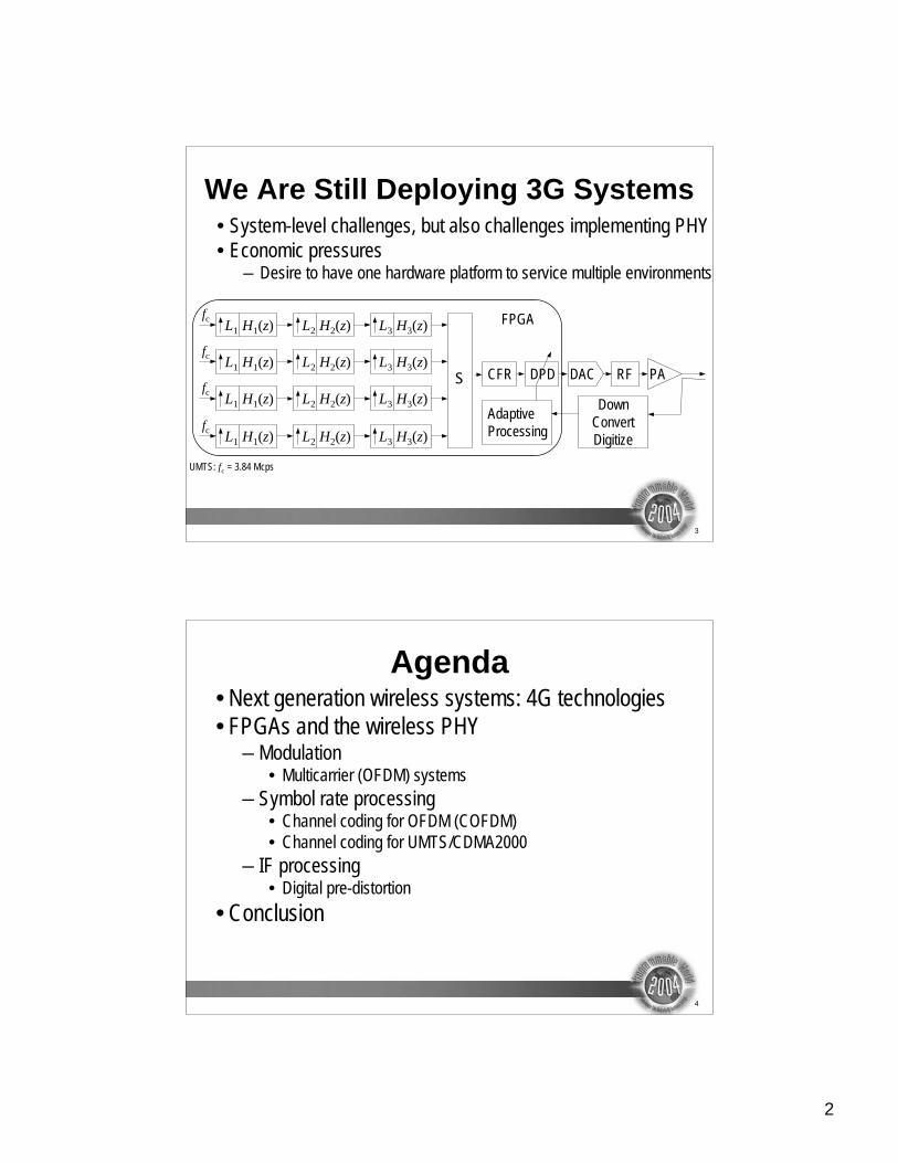
We Are Still Deploying 3G Systems• System-level challenges, but also challenges implementing PHY
• Economic pressures– Desire to have one hardware platform to service multiple environments
UMTS: fc = 3.84 Mcps
S CFR DPD DAC PARF
L1 H1(z) L2 H2(z) L3 H3(z)fc
L1 H1(z) L2 H2(z) L3 H3(z)fc
L1 H1(z) L2 H2(z) L3 H3(z)fc
L1 H1(z) L2 H2(z) L3 H3(z)fc
Adaptive
Processing
FPGA
Down
Convert
Digitize
4
Agenda• Next generation wireless systems: 4G technologies
• FPGAs and the wireless PHY– Modulation
• Multicarrier (OFDM) systems
– Symbol rate processing• Channel coding for OFDM (COFDM)
• Channel coding for UMTS/CDMA2000
– IF processing• Digital pre-distortion
• Conclusion
3
5
4G Wireless• Goal of 4G wireless
– Introduce new technologies to provide higher data rates
and deliver new services
– Integration of existing technologies in a common platform
• 4G requirements still in a fluid state and the
requirements are not defined … but expectations set
6
4G Requirements• Generic architecture
– Enabling integration of existing technologies
• High spectral efficiency
– Offering higher data rates
• High scalability
– Different cell configurations: hot-spot, ad-hoc, bettercoverage
• Low cost
• Future proof
4
7
4G Technologies• Software defined radio
– Requiring heterogeneous computing platforms
– High-performance signal processing
• Tera to petaflop computing
– Design flows and software infrastructure to enable waveform
portability and support different device technologies
• E.g. FPGA and DSP processor
• New modulation and channel access techniques
– MC-CDMA (or OFDM CDMA)
– MC-DS-CDMA
8
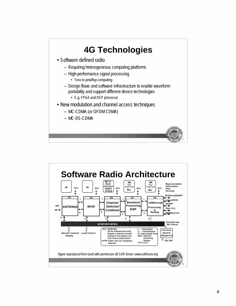
Software Radio Architecture
RF
BB / IFReal/
Complex Digital/
Analog
RF Bits
Aux Aux
RepresentativeInformationFlowFormats
AIR
C
I
MONITOR/CONTROL
Call/Message
Processing &
I/O
C
Routing
Common
System
Equipment
Clock/StrobeRef, Power
Multimedia/WAP
Voice/PSTN
Data/IP
Flow Ctrl
NSS/Network
Ext. Ref
Remote Control/
Display
Local Control
I: Information
C: Control/Status
CC
I/O
C
ANTENNA
I
Aux
BB
Bits
BBText
Flow CntlText
Flow Cntl
Aux: (Optional)
I/O for Antenna Diversity,
Adaptive Antenna Control
Selective Encryption, etc.
Link Processing Control
IF: Intermediate Freq
PSTN: Public Serv ice Telephone
Network
Network
Switching
System
NSS:
Channel
Selector/
Combiner
Baseband
Processing
DSP C
I/O I/O I/O
RF/IF
C
C
C
I I I
Aux Aux
BB: Baseband
figure reproduced from (and with permission of) SDR forum: www.sdrforum.org
5
9
SDR Front-End: MIMO (1)
• The SDR front end is becoming increasingly complex
as the spatial dimension is leveraged
• Mimo: cornerstone of many future wireless
communication systems
• Enormous computation complexity not addressable
by conventional signal processing hardware
10
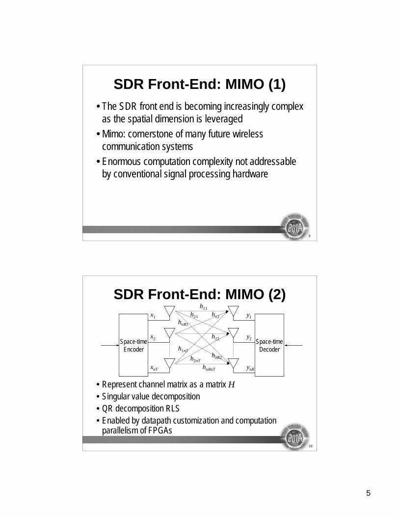
SDR Front-End: MIMO (2)
• Represent channel matrix as a matrix H
• Singular value decomposition
• QR decomposition RLS
• Enabled by datapath customization and computationparallelism of FPGAs
Space-time
Encoder
x1
x2
xnT
Space-time
Decoder
y1
y2
ynR
h11
h21 h12
hnR1
hnRnT
h2nT
h1nT
h22
hnR2
6
11
SDR: Which Computing Paradigm?
• “…This was a highly parallel
machine, before von Neumann
spoiled it”-D. H. Lehmer (1905-1991, U.C.
Berkeley), “A History of Computing in the 20th Century”
• Tubes: 17,468
• Add time: 200 microseconds
• Multiply time: 2,800
microseconds
• Divide time: 24,000 microseconds
• Arithmetic mode: parallel … later serial
ENIAC
12
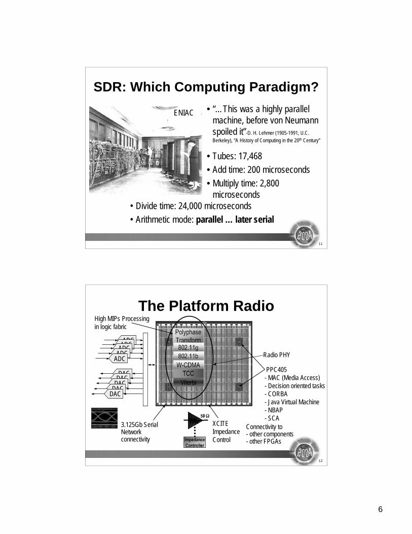
The Platform Radio
3.125Gb SerialNetworkconnectivity
50
Impedance
Controller
XCITE
Impedance
Control
Polyphase
Transform802.11g
802.11b
W-CDMA
TCC
Viterbi
PPC405
- MAC (Media Access)
- Decision oriented tasks
- CORBA
- Java Virtual Machine
- NBAP
- SCA
High MIPs Processing
in logic fabric
ADCADC
ADCADC
ADC
DACDAC
DACDAC
DAC
Connectivity to- other components- other FPGAs
Radio PHY
7
13
Agenda
• Next generation wireless systems: 4G technologies
• FPGAs and the wireless PHY– Modulation
• Multicarrier (OFDM) systems
– Symbol rate processing• Channel coding for OFDM (COFDM) and UMTS/CDMA2000
systems
– IF processing• Digital pre-distortion
• Platform radio example– JTRS radio - Partial reconfiguration in the radio PHY
• Conclusion
14
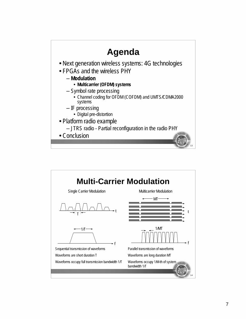
Multi-Carrier Modulation
tT
f
1/T
Sequential transmission of waveforms
Waveforms are short duration T
Waveforms occupy full transmission bandwidth 1/T
f
Parallel transmission of waveforms
Waveforms are long duration MT
Waveforms occupy 1/M-th of system
bandwidth 1/T
1/MT
t
MT
Single Carrier Modulation Multicarrier Modulation
8
15
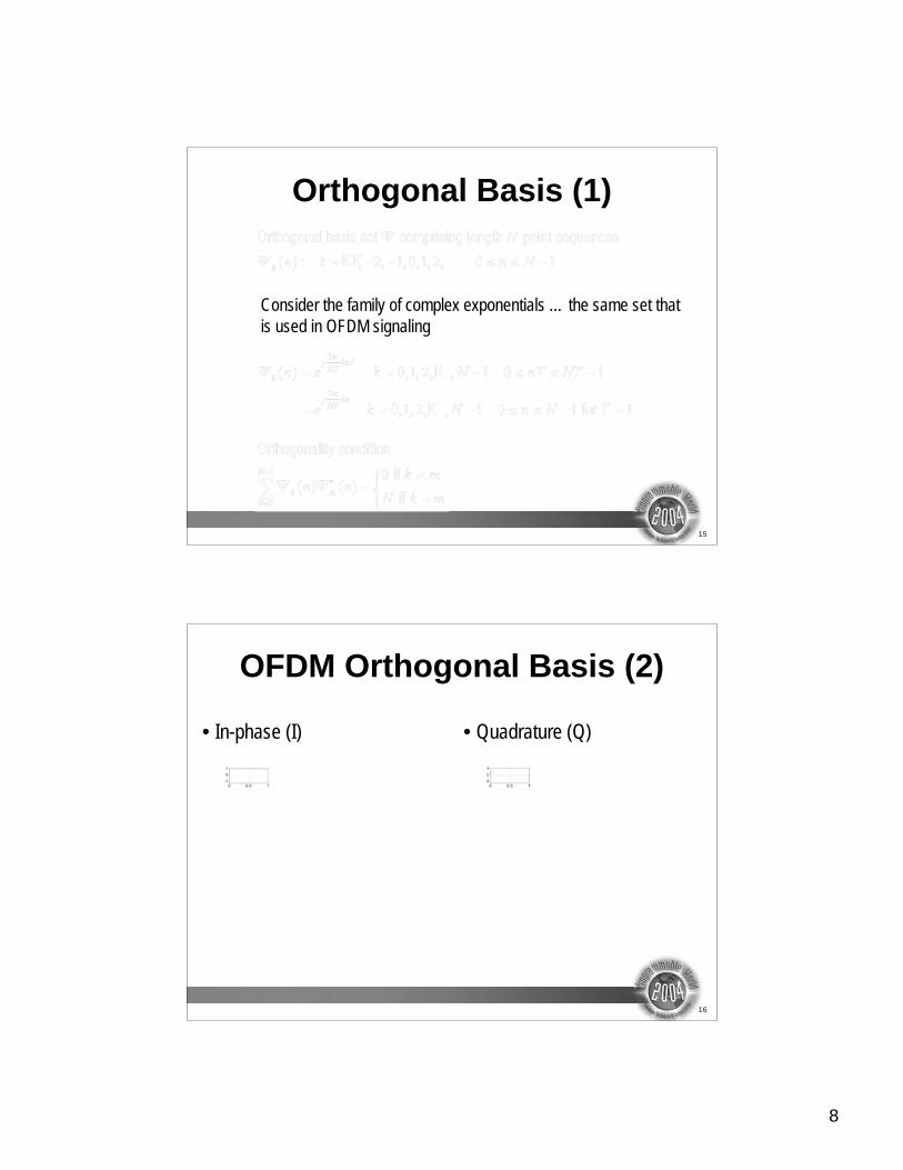
Orthogonal Basis (1)
Consider the family of complex exponentials … the same set that
is used in OFDM signaling
16
OFDM Orthogonal Basis (2)
• In-phase (I) • Quadrature (Q)
9
17
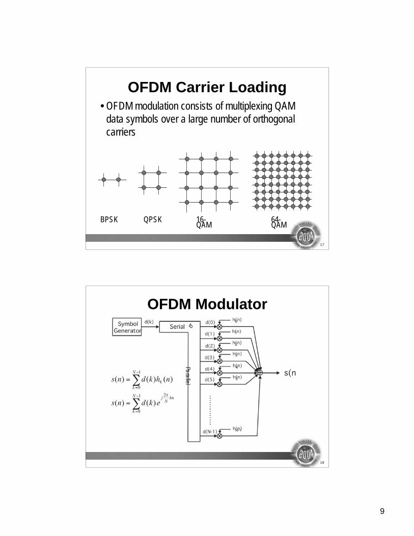
OFDM Carrier Loading• OFDM modulation consists of multiplexing QAM
data symbols over a large number of orthogonal
carriers
16-QAM
64-QAM
QPSKBPSK
18
OFDM Modulator
10
19
OFDM Demodulator
20
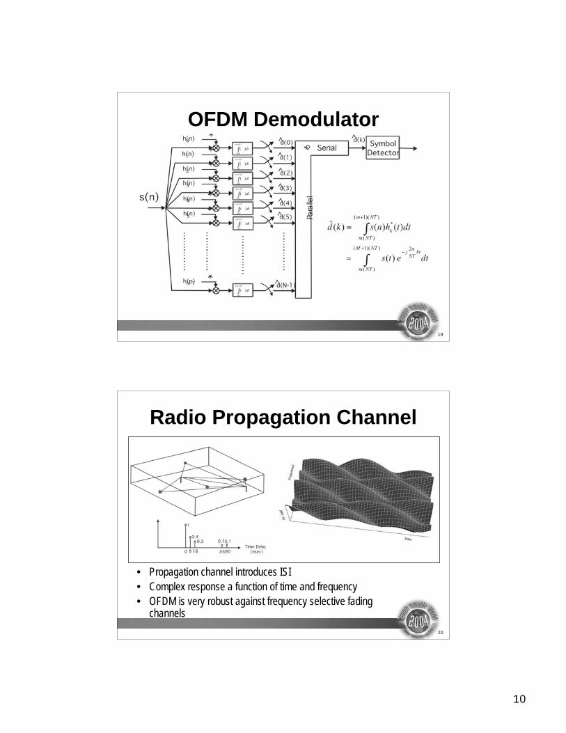
Radio Propagation Channel
• Propagation channel introduces ISI
• Complex response a function of time and frequency
• OFDM is very robust against frequency selective fadingchannels
11
21
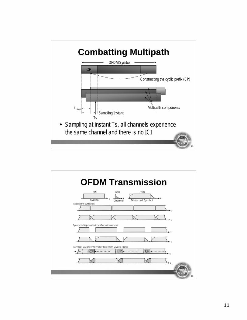
Combatting Multipath
• Sampling at instant Ts, all channels experience
the same channel and there is no ICI
Multipath componentst max
Sampling Instant
Ts
OFDM Symbol
CP
Constructing the cyclic prefix (CP)
22
OFDM Transmission

12
23
System/Channel Effects• Matlab demonstration
24
Properties of OFDM• Advantages
– Efficiently deals with multipath
fading
– Efficiently deals with channel
delay spread
– Enhanced channel capacity
– Adaptively modifies modulation
density
– Robust to narrowband
interference
• Disadvantages
– Sensitive to small carrier
frequency offsets
– Exhibits high peak-to-average
power ratio
– Sensitive to high-frequency
phase noise
– Sensitive to sampling clock
frequency offsets
13
25
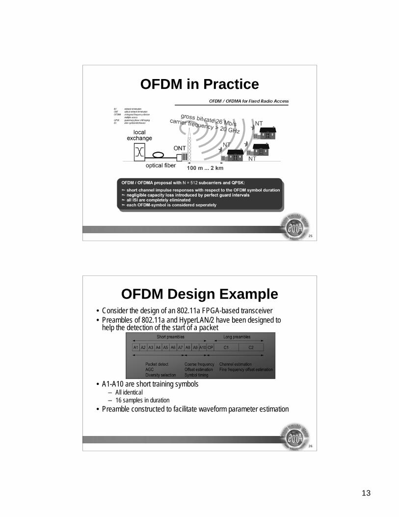
OFDM in Practice
26
OFDM Design Example• Consider the design of an 802.11a FPGA-based transceiver
• Preambles of 802.11a and HyperLAN/2 have been designed tohelp the detection of the start of a packet
• A1-A10 are short training symbols– All identical
– 16 samples in duration
• Preamble constructed to facilitate waveform parameter estimation
A1 A2 A3 A4 A5 A6 A7 A8 A9 A10 CP C1 C2
Packet detectAGC
Diversity selection
Coarse frequencyOffset estimation
Symbol timing
Channel estimationFine frequency offset estimation
Short preambles Long preambles
14
27
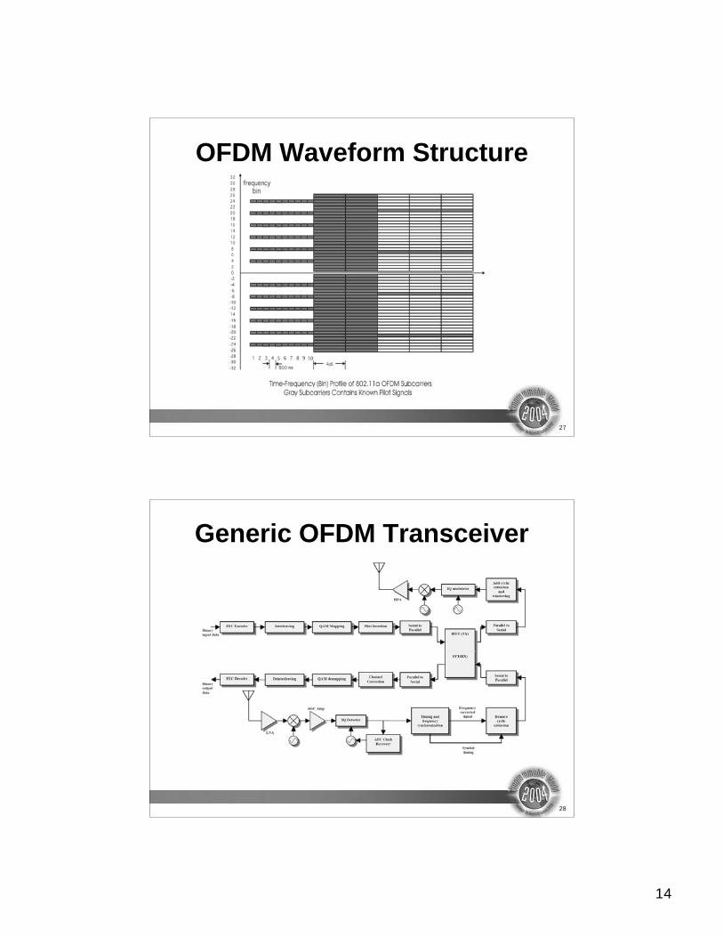
OFDM Waveform Structure
28
Generic OFDM Transceiver
15
29
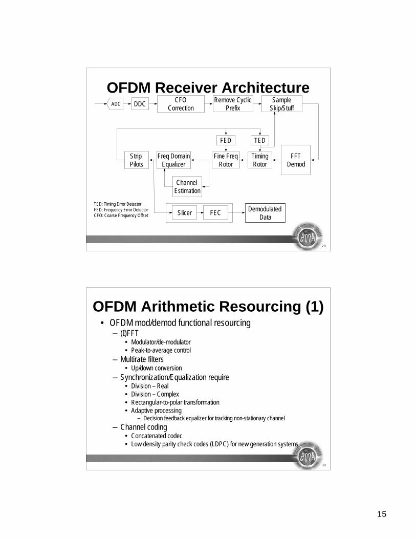
OFDM Receiver ArchitectureADC DDC
CFO
Correction
Remove Cyclic
Prefix
Sample
Skip/Stuff
FFT
Demod
Timing
Rotor
Fine Freq
Rotor
Freq Domain
Equalizer
Channel
Estimation
Strip
Pilots
TEDFED
FECSlicerDemodulated
Data
TED: Timing Error Detector
FED: Frequency Error Detector
CFO: Coarse Frequency Offset
30
OFDM Arithmetic Resourcing (1)• OFDM mod/demod functional resourcing
– (I)FFT• Modulator/de-modulator
• Peak-to-average control
– Multirate filters• Up/down conversion
– Synchronization/Equalization require• Division – Real
• Division – Complex
• Rectangular-to-polar transformation
• Adaptive processing– Decision feedback equalizer for tracking non-stationary channel
– Channel coding• Concatenated codec
• Low density parity check codes (LDPC) for new generation systems

16
31
OFDM Arithmetic Resourcing (2)• Most of the functions are multiplier/MAC intensive
– Embedded multipliers in Virtex-II, Spartan-III, Virtex-II
Pro devices
– Xtreme DSP Slice in new generation Virtex-4 FPGA
• CORDIC particularly useful
– Add/Sub/Shift requirements supported very well in
the FPGA device architecture
32
Xilinx IP Libraries (1)• (I)FFT is the heart of the modulator/demodulator
• Most of the design complexity is associated with
– Synchronization• Timing
• Frequency
– Channel estimation and tracking
– Processing to minimize OFDM waveform peak-to-average (PAR) ratio• Be considerate of system analog up-conversion and power
amplifier
17
33
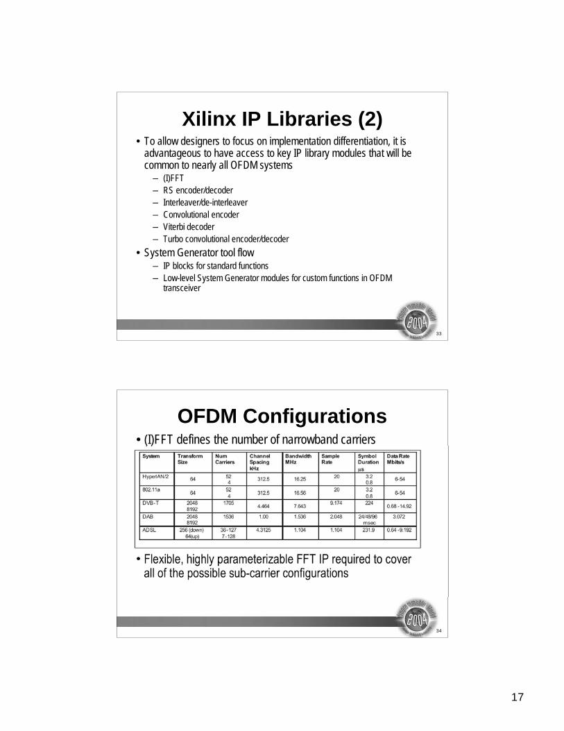
Xilinx IP Libraries (2)• To allow designers to focus on implementation differentiation, it is
advantageous to have access to key IP library modules that will becommon to nearly all OFDM systems
– (I)FFT
– RS encoder/decoder
– Interleaver/de-interleaver
– Convolutional encoder
– Viterbi decoder
– Turbo convolutional encoder/decoder
• System Generator tool flow– IP blocks for standard functions
– Low-level System Generator modules for custom functions in OFDMtransceiver
34
OFDM Configurations• (I)FFT defines the number of narrowband carriers
• Flexible, highly parameterizable FFT IP required to coverall of the possible sub-carrier configurations
18
35
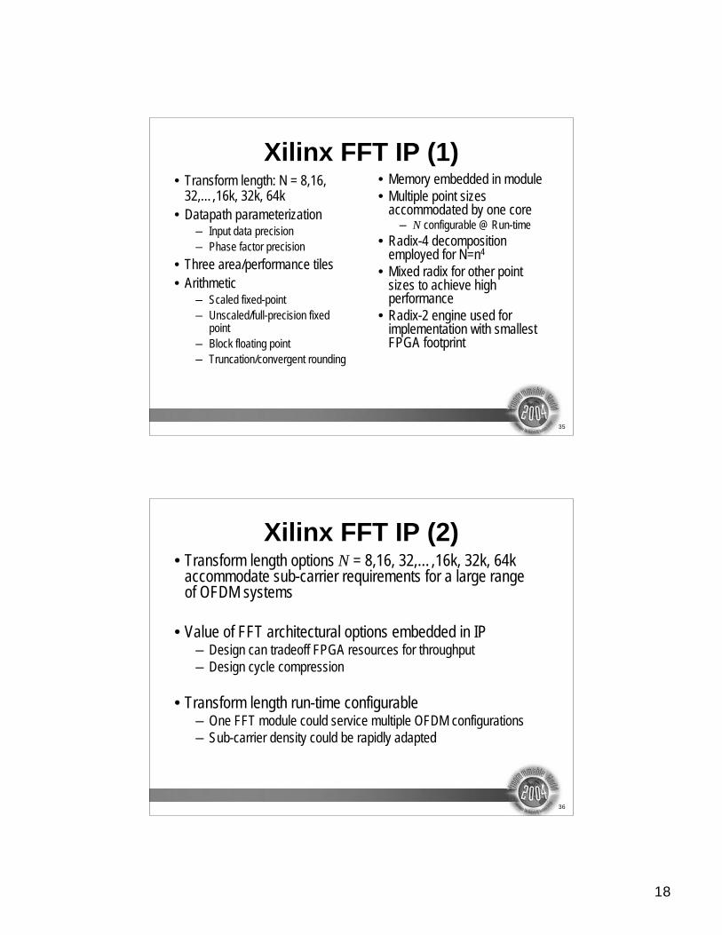
Xilinx FFT IP (1)• Transform length: N = 8,16,
32,…,16k, 32k, 64k
• Datapath parameterization– Input data precision
– Phase factor precision
• Three area/performance tiles
• Arithmetic– Scaled fixed-point
– Unscaled/full-precision fixedpoint
– Block floating point
– Truncation/convergent rounding
• Memory embedded in module
• Multiple point sizesaccommodated by one core
– N configurable @ Run-time
• Radix-4 decompositionemployed for N=n4
• Mixed radix for other pointsizes to achieve highperformance
• Radix-2 engine used forimplementation with smallestFPGA footprint
36
Xilinx FFT IP (2)• Transform length options N = 8,16, 32,…,16k, 32k, 64k
accommodate sub-carrier requirements for a large rangeof OFDM systems
• Value of FFT architectural options embedded in IP– Design can tradeoff FPGA resources for throughput
– Design cycle compression
• Transform length run-time configurable– One FFT module could service multiple OFDM configurations
– Sub-carrier density could be rapidly adapted
19
37
Xilinx FFT IP (3)• FFT IP available for Virtex-E, Virtex-II (Pro), & Spartan-
III devices
• FFT also available for Virtex-4 devices now!
• Virtex-4 port of all DSP IP is available now
38
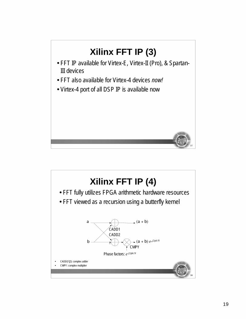
Xilinx FFT IP (4)• FFT fully utilizes FPGA arithmetic hardware resources
• FFT viewed as a recursion using a butterfly kernel
a
b
(a + b)
Phase factors: e-j2pk/N
(a + b) e-j2pk/N
CADD1
CADD2
CMPY
• CADD{1|2}: complex adder
• CMPY: complex multiplier
20
39
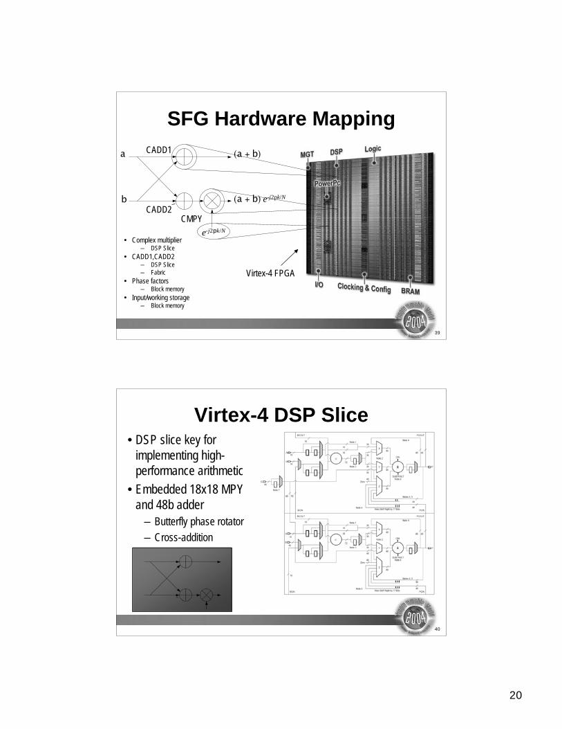
SFG Hardware Mapping
• Complex multiplier– DSP Slice
• CADD1,CADD2– DSP Slice
– Fabric
• Phase factors– Block memory
• Input/working storage– Block memory
a
b
(a + b)
(a + b) e-j2pk/N
CADD1
CADD2CMPY
e-j2pk/N
Virtex-4 FPGA
40
Virtex-4 DSP Slice• DSP slice key for
implementing high-
performance arithmetic
• Embedded 18x18 MPY
and 48b adder
– Butterfly phase rotator
– Cross-addition
21
41
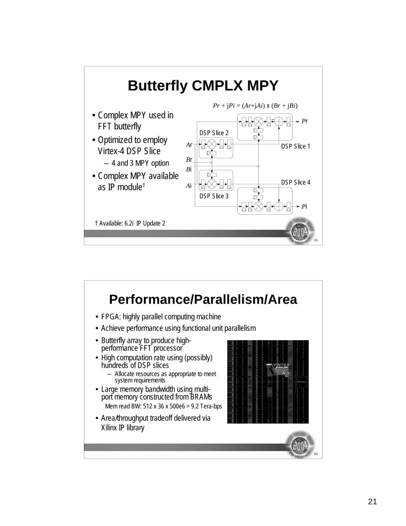
Butterfly CMPLX MPY
• Complex MPY used in
FFT butterfly
• Optimized to employ
Virtex-4 DSP Slice
– 4 and 3 MPY option
• Complex MPY available
as IP module†
Ar
Br
Ai
Bi
Pi
Pr
DSP Slice 1
DSP Slice 4
DSP Slice 2
DSP Slice 3
Pr + jPi = (Ar+jAi) x (Br + jBi)
† Available: 6.2i IP Update 2
42
Performance/Parallelism/Area• FPGA: highly parallel computing machine
• Achieve performance using functional unit parallelism
• Area/throughput tradeoff delivered via
Xilinx IP library
• Butterfly array to produce high-performance FFT processor
• High computation rate using (possibly)hundreds of DSP slices
– Allocate resources as appropriate to meetsystem requirements
• Large memory bandwidth using multi-port memory constructed from BRAMs
Mem read BW: 512 x 36 x 500e6 = 9.2 Tera-bps
22
43
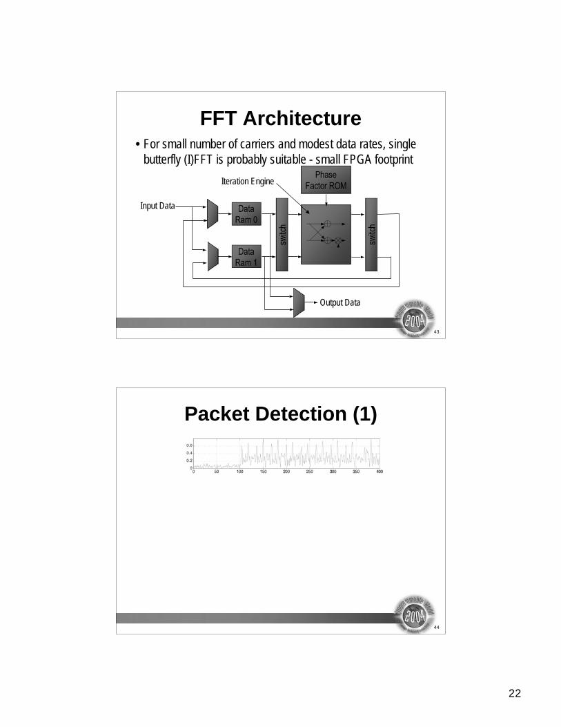
FFT Architecture• For small number of carriers and modest data rates, single
butterfly (I)FFT is probably suitable - small FPGA footprint
switc
h
Phase
Factor ROM
Data
Ram 0
Data
Ram 1
switc
h
Output Data
Input Data
Iteration Engine
44
Packet Detection (1)
23
45
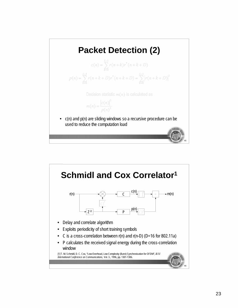
Packet Detection (2)
• c(n) and p(n) are sliding windows so a recursive procedure can be
used to reduce the computation load
46
Schmidl and Cox Correlator1
• Delay and correlate algorithm
• Exploits periodicity of short training symbols
• C is a cross-correlation between r(n) and r(n-D) (D=16 for 802.11a)
• P calculates the received signal energy during the cross-correlation
window[1] T. M. Schmidl, D. C. Cox, “Low-Overhead, Low Complexity (Burst) Synchronization for OFDM”, IEEE
International Conference on Communications, Vol. 3., 1996, pp. 1301-1306.
Z-D
C
P
r(n)c(n)
p(n)
m(n)

24
47
D QC
E
D QC
E
D QC
E
D QC
E
LUTIN
CECL
K
ADDRESS
OUT
CASCADE
• SRL16 can dramatically increase FPGA compute density by enabling the construction of
efficient TDM hardware structures and correlation functions
• Enables highly efficient implementations of multi-channel datapaths
• Unique to Xilinx FPGAs
FPGA Logic Slice: SRL16
48
CIC Filter
CIC Filterz-16
¸ Threshold
d
*
*
r(0)
r(16) c(16)
Preamble
Detect
Preamble Detector Implementation
z-1
z-16
CIC Filter
DSP Slice
or fabric
Complex MPYs implemented using DSP Slice for high-speed operation
SRL16
B
• SRL16 and adder co-located in a logic slice
• B-bit datapath– B/2 logic slices

25
49
CORDIC Arithmetic• Frequently find CORDIC [1][2] processing useful for
FPGA computing
• Rich suite of functions: atan(Q/I), magnitude, sqrt, ln, …
[1] J. E. Volder, “The CORDIC Trigonometric Computing Technique”, IRE Trans. On Electronic
Computers, Vol. EC-8, 1959, pp. 330-334.
[2] Yu Hen Hu, “CORDIC-Based VLSI Architectures for Digital Signal Processing”, IEEE Signal
Processing Magazine, pp. 17-34, July 1992.
50
CORDIC Processor Engine• Example CORDIC
processing engine
– Rotation mode
• Simple add/sub/shift
structure well-suited to
FPGA architecture
z-1-
-
SGNROM
x0
y0
2-i
2-i
xi+1
yi+1
z-1
z-1
tan-1(2-i)
i
Initial condition q
zi
26
51
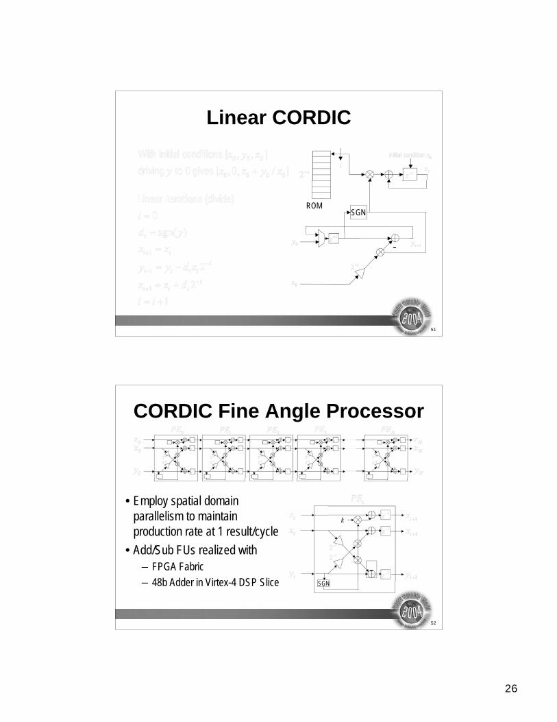
Linear CORDIC
-
SGNROM
52
CORDIC Fine Angle Processor
• Employ spatial domain
parallelism to maintain
production rate at 1 result/cycle
• Add/Sub FUs realized with
– FPGA Fabric
– 48b Adder in Virtex-4 DSP Slice
- - - - -
SGN
-
k

27
53
Packet Detector
• Fully parallel design– 473 slices
– 12 embedded MPY
– fclk ~200 MHz (Virtex-II Pro)
– Potential for hardware folding to reduce MPY count
54
CORDIC Employed in OFDM PHY
ADC DDCCFO
Correction
Remove Cyclic
Prefix
Sample
Skip/Stuff
FFT
Demod
Timing
Rotor
Fine Freq
Rotor
Freq Domain
Equalizer
Channel
Estimation
Strip
Pilots
TEDFED
FECSlicerDemodulated
Data
CORDIC: R-2-P
Packet Detect Long Preamble CorrelatorCORDIC: Div.
CORDIC: Complex Div.
CORDIC: R-2-P
TED: Timing Error DetectorFED: Frequency Error Detector
CFO: Coarse Frequency Offset
28
55
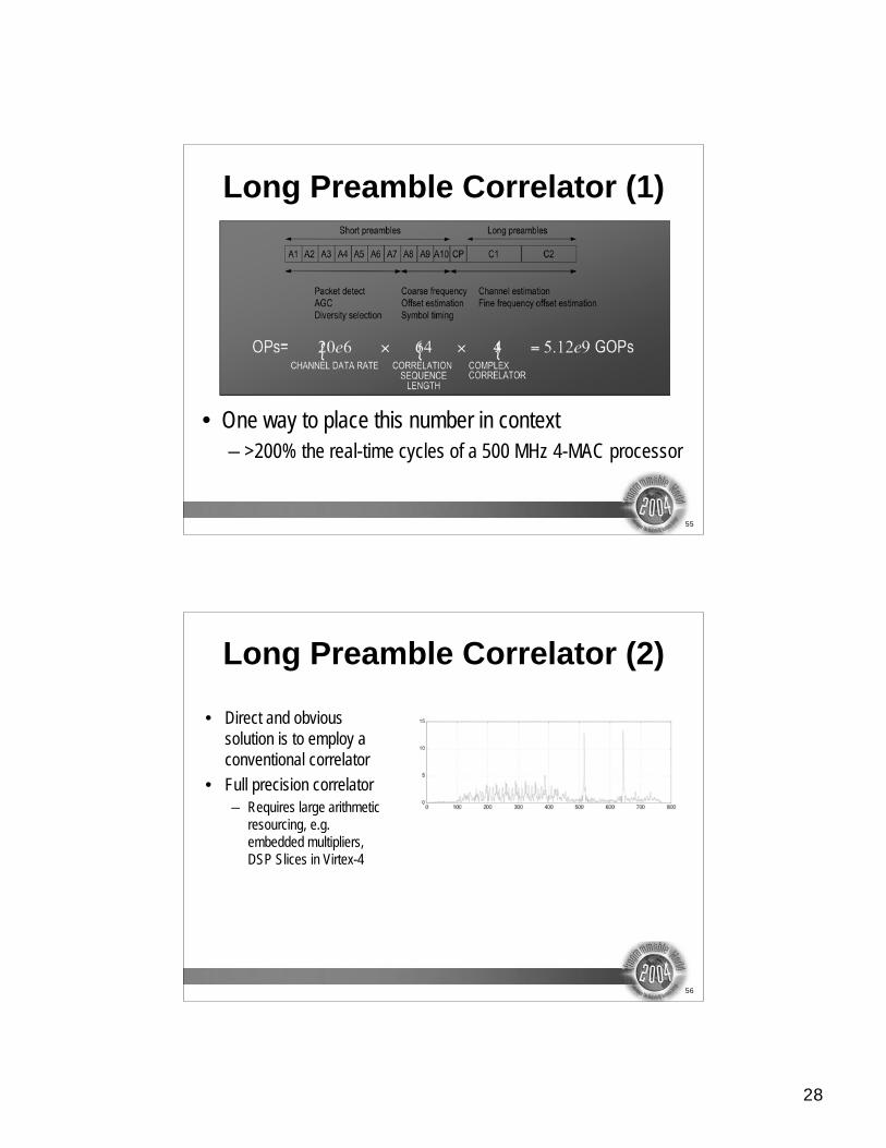
Long Preamble Correlator (1)
• One way to place this number in context
– >200% the real-time cycles of a 500 MHz 4-MAC processor
A1 A2 A3 A4 A5 A6 A7 A8 A9 A10 CP C1 C2
Packet detect
AGC
Diversity selection
Coarse frequency
Offset estimation
Symbol timing
Channel estimation
Fine frequency offset estimation
Short preambles Long preambles
56
Long Preamble Correlator (2)
• Direct and obvious
solution is to employ a
conventional correlator
• Full precision correlator
– Requires large arithmetic
resourcing, e.g.
embedded multipliers,
DSP Slices in Virtex-4
29
57
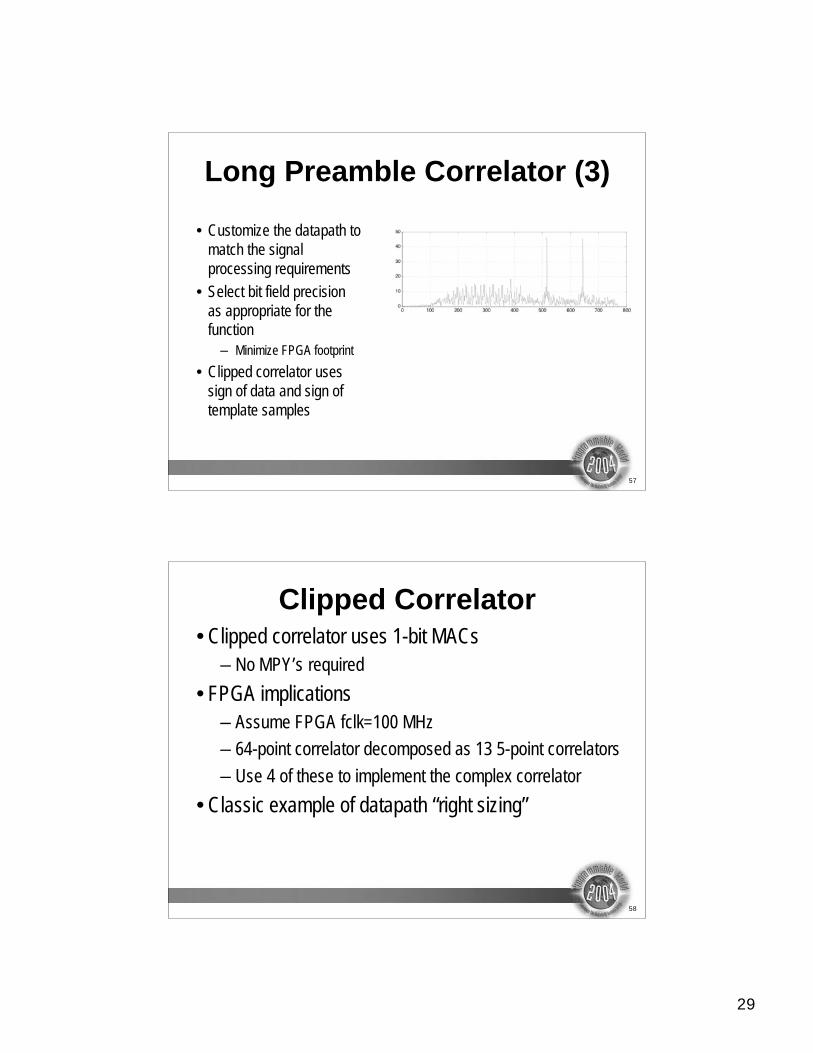
Long Preamble Correlator (3)
• Customize the datapath to
match the signal
processing requirements
• Select bit field precision
as appropriate for the
function
– Minimize FPGA footprint
• Clipped correlator uses
sign of data and sign of
template samples
58
Clipped Correlator• Clipped correlator uses 1-bit MACs
– No MPY’s required
• FPGA implications
– Assume FPGA fclk=100 MHz
– 64-point correlator decomposed as 13 5-point correlators
– Use 4 of these to implement the complex correlator
• Classic example of datapath “right sizing”
30
59
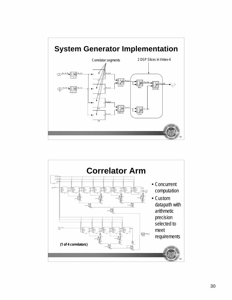
System Generator Implementation
Correlator segments 2 DSP Slices in Virtex-4
60
Correlator Arm
• Concurrent
computation
• Custom
datapath with
arithmetic
precision
selected to
meet
requirements
(1 of 4 correlators)
31
61
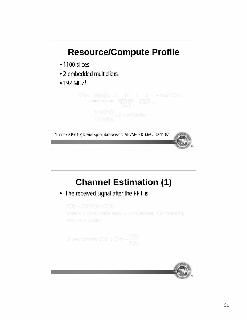
Resource/Compute Profile
• 1100 slices
• 2 embedded multipliers
• 192 MHz1
1. Virtex-2 Pro (-7) Device speed data version: ADVANCED 1.69 2002-11-07
62
• The received signal after the FFT is
Channel Estimation (1)

32
63
Channel Estimation (2)
• Packet-based OFDMtypically employs apreamble
– View this as a Widebandchannel probe
• Use it to train theequalizer
• Fully parallelimplementation ofestimator and equalizer
– 776 slices
– 10 multipliers
– 4 block RAMs
64
Carrier Frequency Offset Estimation
• Multiple techniques for CFO estimation/correction
• CFO can be estimated from the modulated data
stream
– Unlike Moose algorithm that relies on known and
identical FFT symbols
• Recall conjugate product of two complex phasors
results in the difference vector that can be used
to compute the angle between the input phasors
33
65
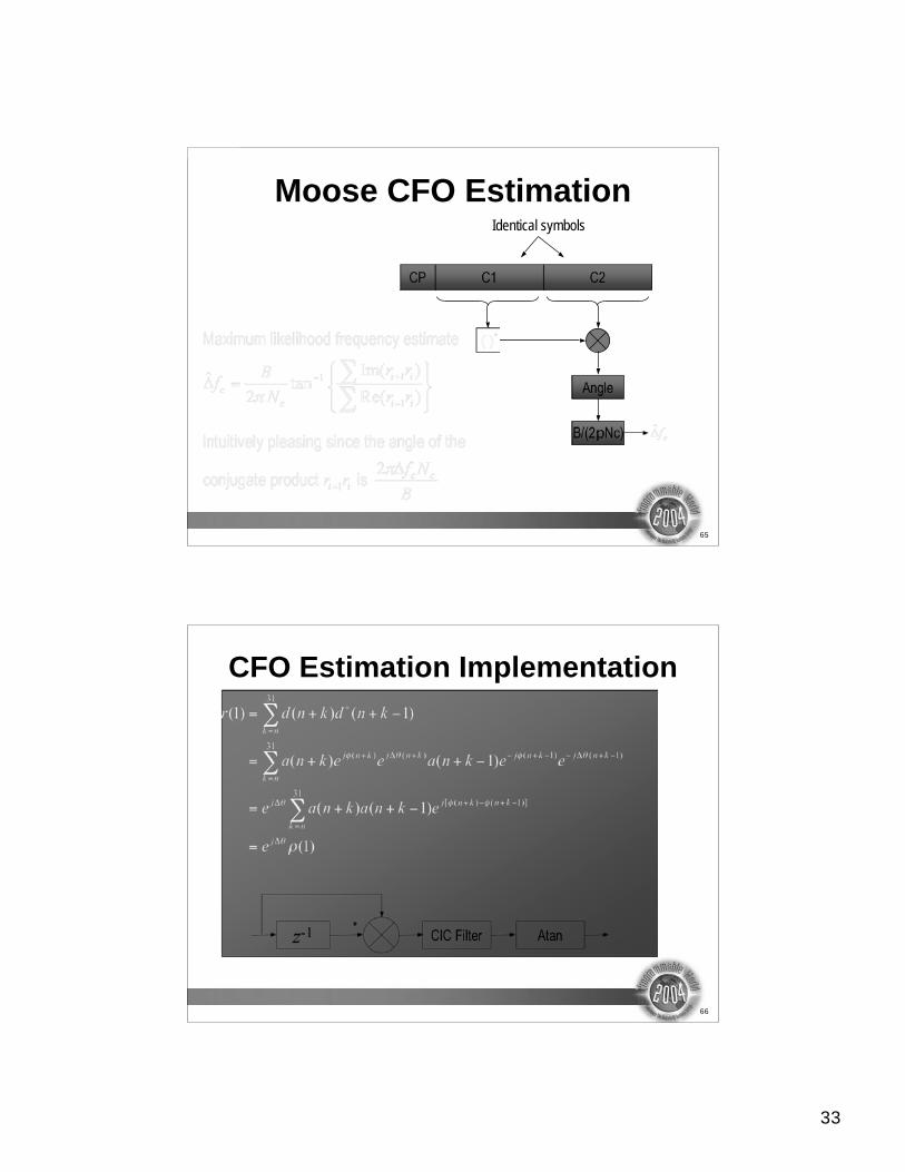
Moose CFO Estimation
C1 C2CP
Identical symbols
Angle
B/(2pNc)
66
CFO Estimation Implementation
z-1 CIC Filter Atan*

34
67
Power Amplifier Considerations (1)
• Cost of processing BW digitally has been lower than cost
of analog signal processing for many years
• Digital processing benefits from Moore, analog does not
• Preference to use low-cost power amplifiers with digital
compensation
• Primarily two issues to focus on
– Linearity
– Efficiency
68
Power Amplifier Considerations (2)• Linearity
– Class A linear amplifier: Expensive
– Class AB non-linear amplifier: low(er) cost
– Defer linearity issue to the digital domain and benefit from continually falling costof DSP
• E.g. Virtex-4 SX Digital Signal Processor
– Wide bandwidth: significant arithmetic requirements to linearize
• Resourced with parallel FPGA processing
• Efficiency– Desire to reduce transmission waveform peak-to-average power ratio (PAPR)
• Lower cost PA palette using plastic packaging for power devices
• Multi-carrier systems– One PA, multiple carriers e.g. 4-carrier UMTS
– Enabled using DSP techniques

35
69
OFDM PAPR• Amplitude distribution of OFDM signal approximately
Gaussian for large number of carriers
• OFDM waveform will occasionally generate very high peaks
– Linear PA
• Expensive
– Large backoff
• Power inefficient
• Defer problem to digital domain and process signal before
presenting to analog up-conversion/amplification chain
– Cost effective from a system perspective
• PAPR control can be arithmetically expensive
70
OFDM PAPR
• Peak-to-average power
ratio
• Probability that PAPR
exceeds a threshold Y
36
71
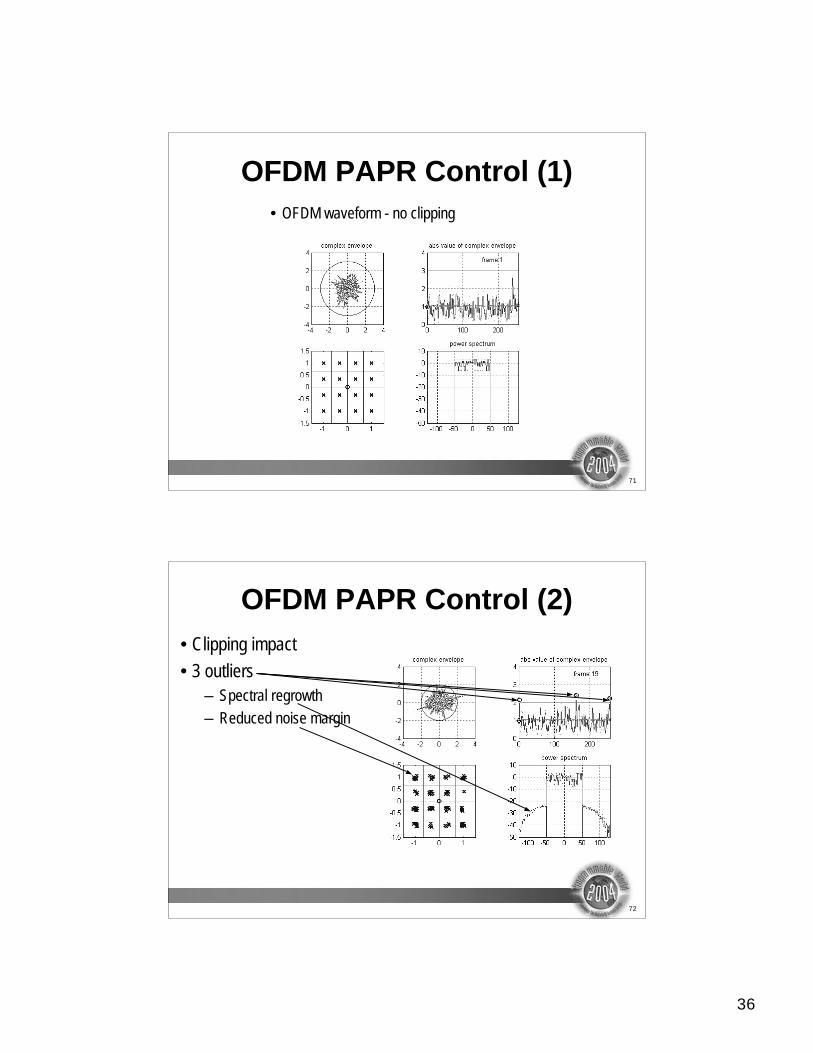
OFDM PAPR Control (1)
• OFDM waveform - no clipping
72
OFDM PAPR Control (2)
• Clipping impact
• 3 outliers
– Spectral regrowth
– Reduced noise margin
37
73
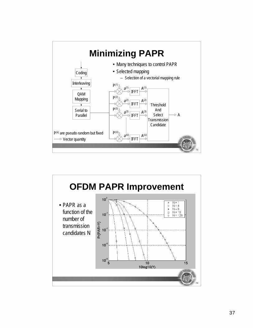
Minimizing PAPR• Many techniques to control PAPR
• Selected mapping
– Selection of a vectorial mapping rule
Coding
Interleaving
QAM
Mapping
Serial to
Parallel
P(1)
a(1)
IFFTA(1)
Threshold
And
Select
Transmission
Candidate
P(2)
a(2)
IFFTA(2)
P(3)
a(3)
IFFTA(3)
P(U)
a(U)
IFFTA(U)
A
P(k) are pseudo random but fixed
Vector quantity
74
OFDM PAPR Improvement
• PAPR as a
function of the
number of
transmission
candidates N
38
75
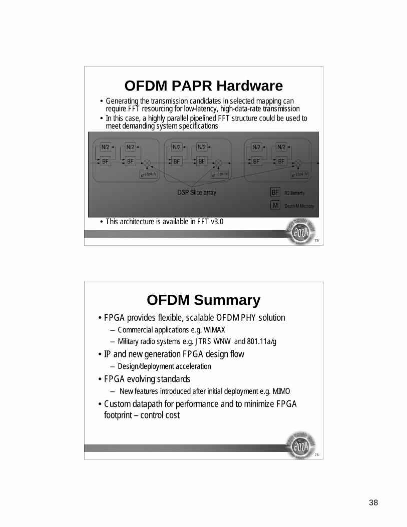
OFDM PAPR Hardware• Generating the transmission candidates in selected mapping can
require FFT resourcing for low-latency, high-data-rate transmission
• In this case, a highly parallel pipelined FFT structure could be used tomeet demanding system specifications
• This architecture is available in FFT v3.0
M Depth M Memory
BF R2 Butterfly
BF
N/2
BF
N/2
e-j2pk/N
BF
N/2
BF
N/2
e-j2pk/N
BF
N/2
BF
N/2
e-j2pk/N
DSP Slice array
76
OFDM Summary• FPGA provides flexible, scalable OFDM PHY solution
– Commercial applications e.g. WiMAX
– Military radio systems e.g. JTRS WNW and 801.11a/g
• IP and new generation FPGA design flow
– Design/deployment acceleration
• FPGA evolving standards
– New features introduced after initial deployment e.g. MIMO
• Custom datapath for performance and to minimize FPGA
footprint – control cost
39
77
Agenda• Next generation wireless systems: 4G technologies
• FPGAs and the wireless PHY– Modulation
• Multicarrier (OFDM) systems
– Symbol rate processing• Channel coding for OFDM (COFDM)
• Channel coding UMTS/CDMA2000
– IF processing• Digital pre-distortion
• Conclusion
78
Coded OFDM (COFDM) (1)• In most real systems, COFDM is employed
• For sub-carriers in deep fades, forward error correction
across the sub-carriers is used with variable coding rates
• Many channel coding techniques employed in various OFDM
PHYs
– Convolutional code with block interleaving e.g. 801.11{a|g}
– Concatenated codes
– Turbo convolutional codes
– Low density parity check codes (LDPC)
40
79
Coded OFDM (COFDM) (2)• Xilinx DSP IP library provides a rich suite of channel
coding solutions
– RS, Convolutional w/ Viterbi decoder, Turbo
convolutional and product codes, block convolutional (de-
)interleavers
• Delivered via The Core Generator System
– Use in HDL design flows
• Channel coding modules also available in System
Generator for DSP design flow
80
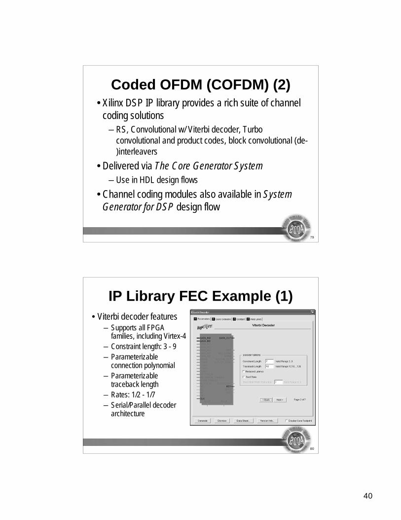
IP Library FEC Example (1)
• Viterbi decoder features– Supports all FPGA
families, including Virtex-4
– Constraint length: 3 - 9
– Parameterizableconnection polynomial
– Parameterizabletraceback length
– Rates: 1/2 - 1/7
– Serial/Parallel decoderarchitecture
41
81
IP Library FEC Example (2)
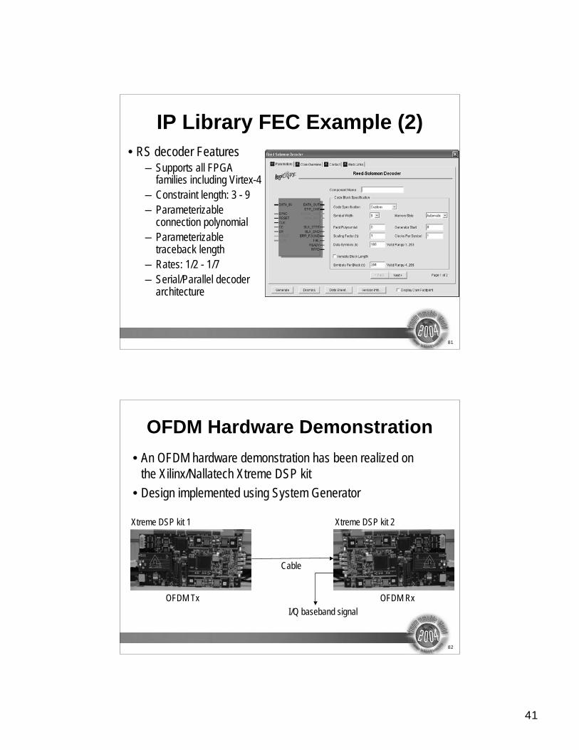
• RS decoder Features– Supports all FPGA
families including Virtex-4
– Constraint length: 3 - 9
– Parameterizableconnection polynomial
– Parameterizabletraceback length
– Rates: 1/2 - 1/7
– Serial/Parallel decoderarchitecture
82
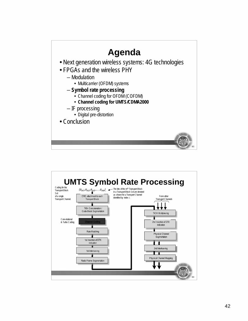
OFDM Hardware Demonstration
• An OFDM hardware demonstration has been realized on
the Xilinx/Nallatech Xtreme DSP kit
• Design implemented using System Generator
Cable
OFDM Tx OFDM Rx
I/Q baseband signal
Xtreme DSP kit 1 Xtreme DSP kit 2
42
83
Agenda• Next generation wireless systems: 4G technologies
• FPGAs and the wireless PHY– Modulation
• Multicarrier (OFDM) systems
– Symbol rate processing• Channel coding for OFDM (COFDM)
• Channel coding for UMTS/CDMA2000
– IF processing• Digital pre-distortion
• Conclusion
84
UMTS Symbol Rate Processing
Physical Channel Mapping
2nd Interleav ing
TrBk Concatenation /
Code Block Segmentation
Radio Frame Segmentation
1st Interleav ing
Rate Matching
Channel Coding
TrCH Multiplex ing
Physical Channel
Segmentation
2nd Interleav ing
Physical Channel Mapping
Convolutional
& Turbo Coding
1st Insertion of DTX
indication
2nd Insertion of DTX
indication
CRC attachment to each
Transport Block
The bits of the mth Transport Block
in a Transport Block Set are denoted
as shown for a Transport Channel
identified by index i.From other
Transport Channels
Coding for the
Transport Block
Set
of a single
Transport Channel.
(aim1,aim2,aim3,…..aimA),
43
85
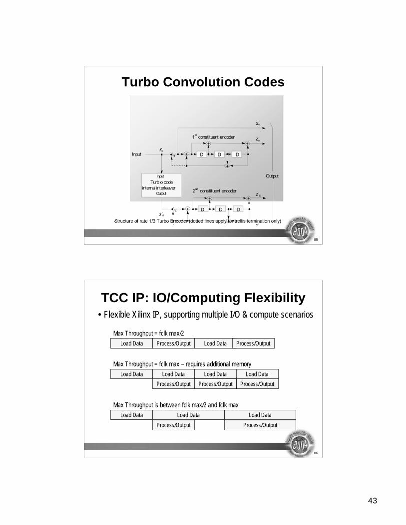
Turbo Convolution Codes
Structure of rate 1/3 Turbo Encoder (dotted lines apply for trellis termination only)
86
TCC IP: IO/Computing Flexibility
Max Throughput = fclk max/2
Load Data
Process/Output Process/Output
Load DataLoad Data Load Data
Process/Output
Max Throughput = fclk max – requires additional memory
Load Data
Process/Output
Load DataLoad Data
Process/Output
Max Throughput is between fclk max/2 and fclk max
Load Data Process/Output Load Data Process/Output
• Flexible Xilinx IP, supporting multiple I/O & compute scenarios
44
87
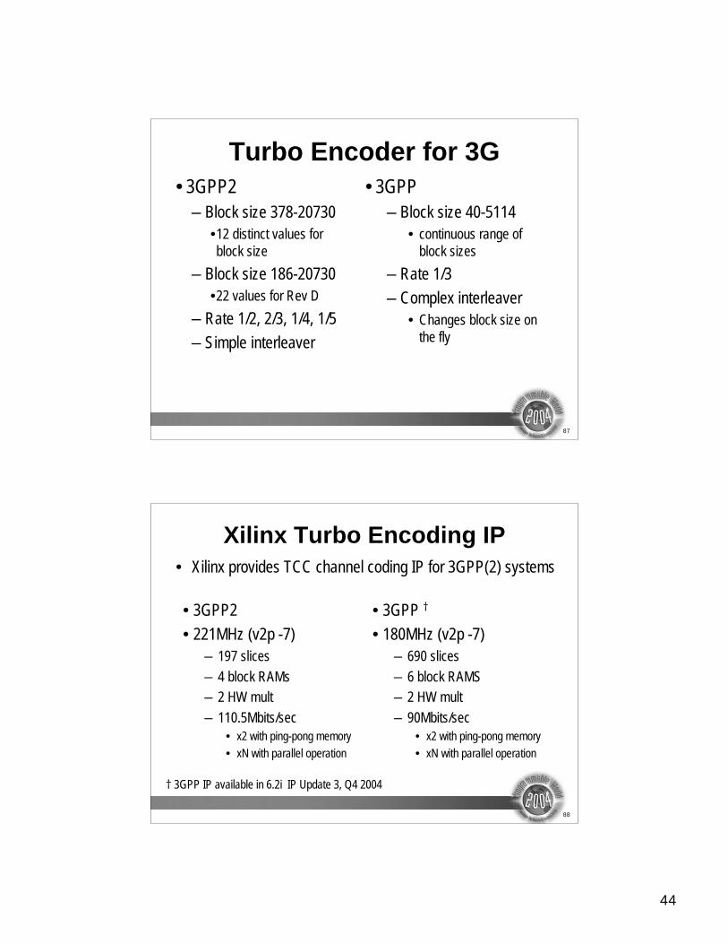
Turbo Encoder for 3G
• 3GPP2
– Block size 378-20730
•12 distinct values for
block size
– Block size 186-20730
•22 values for Rev D
– Rate 1/2, 2/3, 1/4, 1/5
– Simple interleaver
• 3GPP
– Block size 40-5114
• continuous range of
block sizes
– Rate 1/3
– Complex interleaver
• Changes block size on
the fly
88
Xilinx Turbo Encoding IP
• 3GPP2
• 221MHz (v2p -7)
– 197 slices
– 4 block RAMs
– 2 HW mult
– 110.5Mbits/sec
• x2 with ping-pong memory
• xN with parallel operation
• 3GPP †
• 180MHz (v2p -7)
– 690 slices
– 6 block RAMS
– 2 HW mult
– 90Mbits/sec
• x2 with ping-pong memory
• xN with parallel operation
• Xilinx provides TCC channel coding IP for 3GPP(2) systems
† 3GPP IP available in 6.2i IP Update 3, Q4 2004
45
89
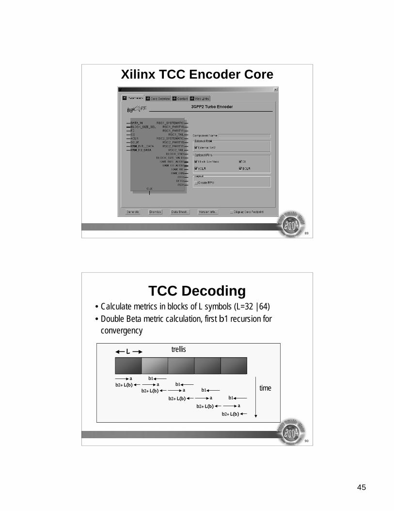
Xilinx TCC Encoder Core
90
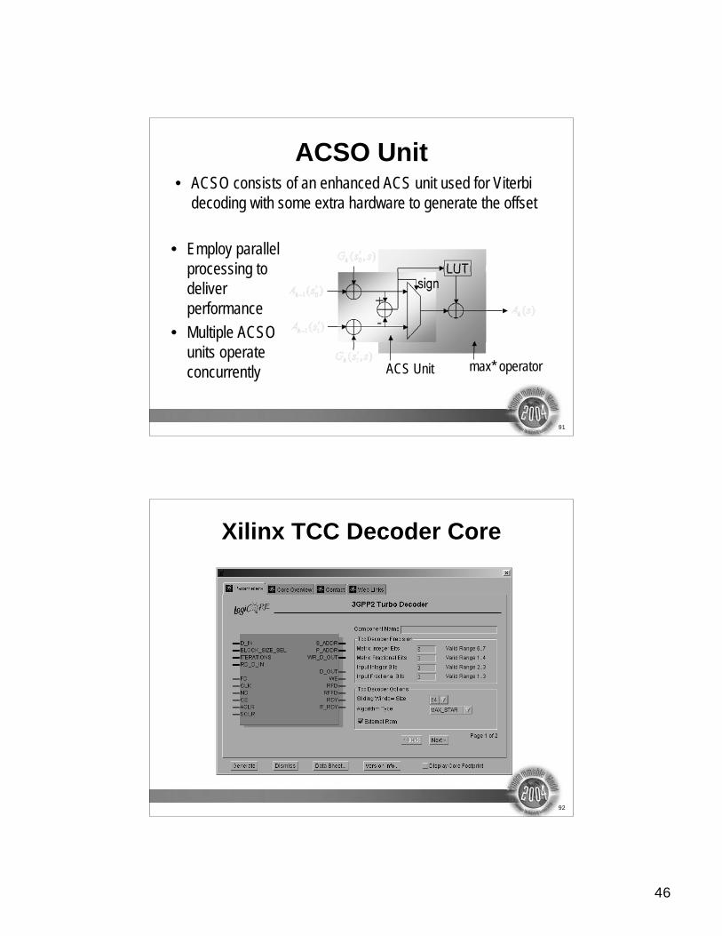
TCC Decoding• Calculate metrics in blocks of L symbols (L=32 | 64)
• Double Beta metric calculation, first b1 recursion for
convergency
L
a b1
b2+ L(b) a b1
b2+ L(b) a b1
b2+ L(b) a b1
b2+ L(b) a
b2+ L(b)
time
trellis
46
91
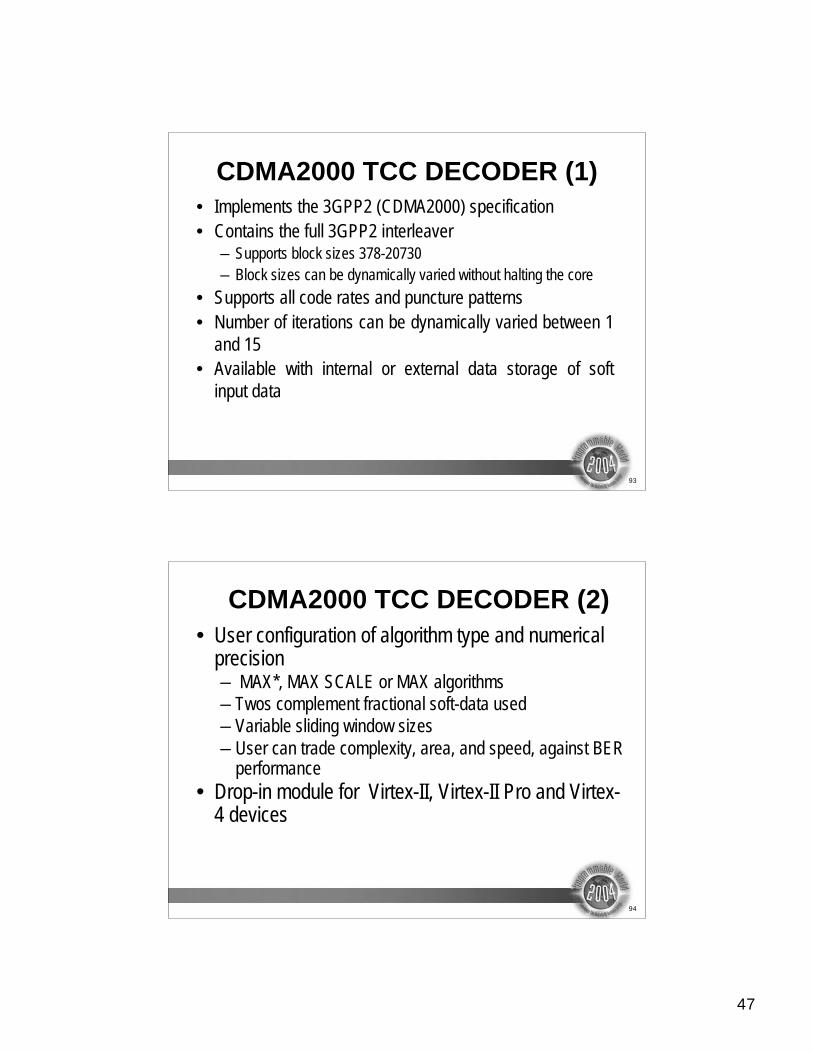
ACSO Unit• ACSO consists of an enhanced ACS unit used for Viterbi
decoding with some extra hardware to generate the offset
+
-
LUTsign
ACS Unit max* operator
• Employ parallel
processing to
deliver
performance
• Multiple ACSO
units operate
concurrently
92
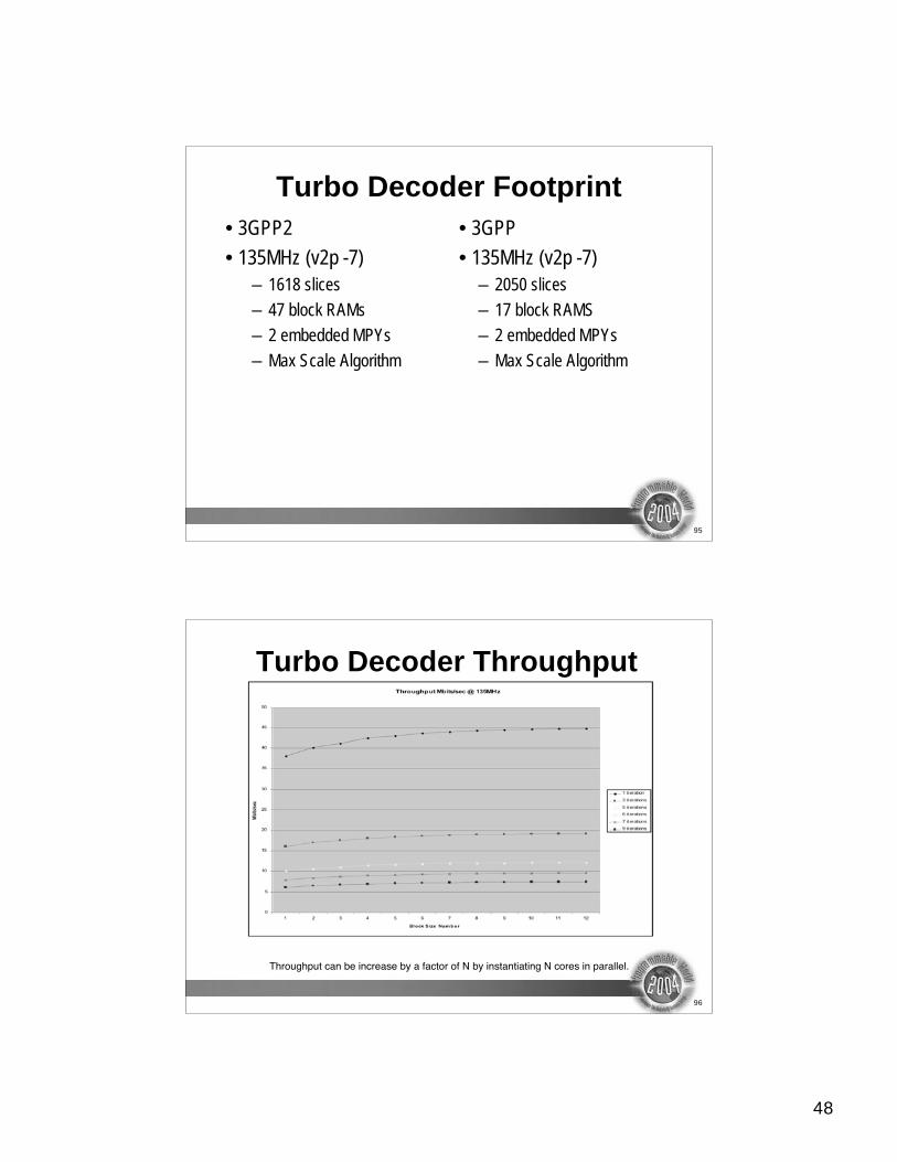
Xilinx TCC Decoder Core
47
93
CDMA2000 TCC DECODER (1)
• Implements the 3GPP2 (CDMA2000) specification
• Contains the full 3GPP2 interleaver– Supports block sizes 378-20730
– Block sizes can be dynamically varied without halting the core
• Supports all code rates and puncture patterns
• Number of iterations can be dynamically varied between 1
and 15
• Available with internal or external data storage of soft
input data
94
CDMA2000 TCC DECODER (2)
• User configuration of algorithm type and numericalprecision– MAX*, MAX SCALE or MAX algorithms
– Twos complement fractional soft-data used
– Variable sliding window sizes
– User can trade complexity, area, and speed, against BERperformance
• Drop-in module for Virtex-II, Virtex-II Pro and Virtex-4 devices
48
95
Turbo Decoder Footprint
• 3GPP2
• 135MHz (v2p -7)
– 1618 slices
– 47 block RAMs
– 2 embedded MPYs
– Max Scale Algorithm
• 3GPP
• 135MHz (v2p -7)
– 2050 slices
– 17 block RAMS
– 2 embedded MPYs
– Max Scale Algorithm
96
Turbo Decoder Throughput
Throughput can be increase by a factor of N by instantiating N cores in parallel.
49
97
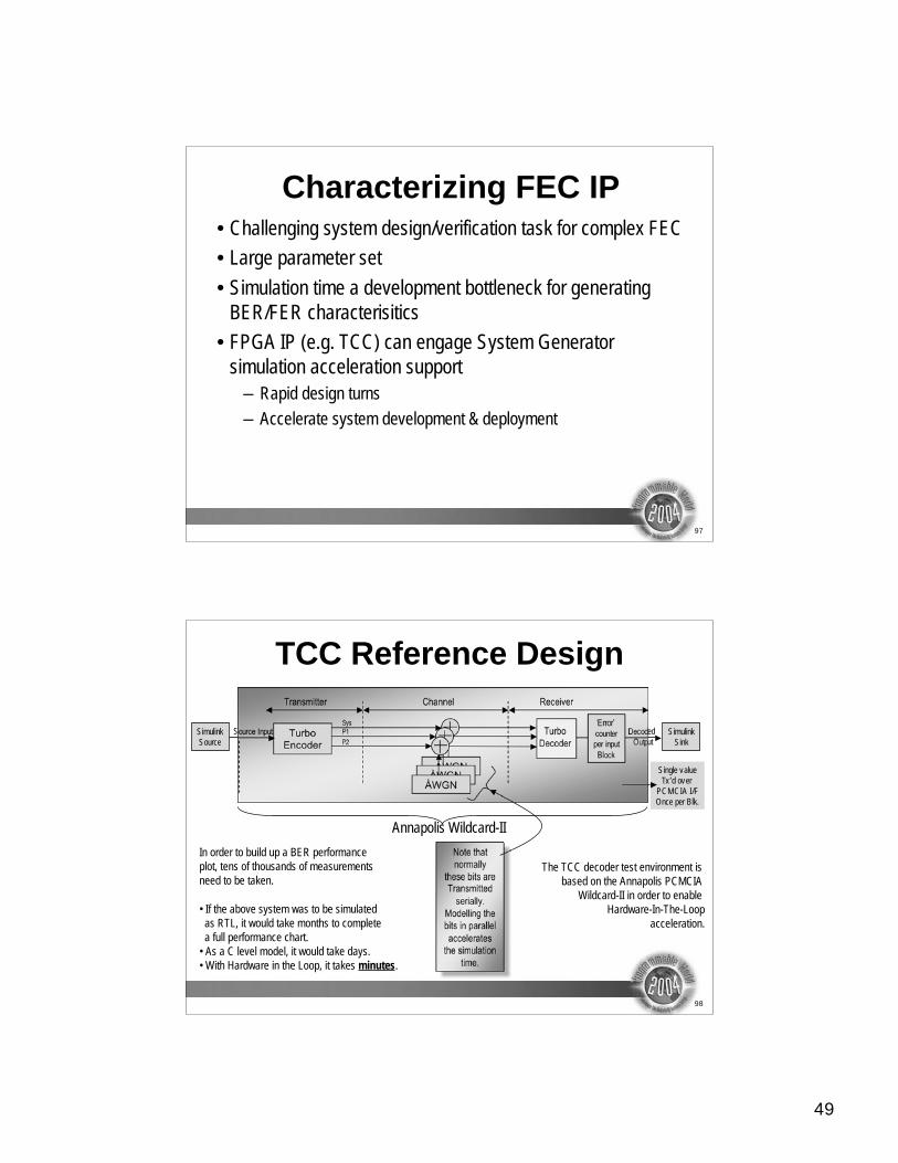
Characterizing FEC IP• Challenging system design/verification task for complex FEC
• Large parameter set
• Simulation time a development bottleneck for generating
BER/FER characterisitics
• FPGA IP (e.g. TCC) can engage System Generator
simulation acceleration support
– Rapid design turns
– Accelerate system development & deployment
98
In order to build up a BER performance
plot, tens of thousands of measurements
need to be taken.
• If the above system was to be simulated
as RTL, it would take months to complete
a full performance chart.
• As a C level model, it would take days.
• With Hardware in the Loop, it takes minutes.
TCC Reference Design
ÀWGN
Transmitter ReceiverChannel
ÀWGNÀWGN
TurboEncoder
SysP1
P2
Decoded
Output
The TCC decoder test environment is
based on the Annapolis PCMCIA
Wildcard-II in order to enable
Hardware-In-The-Loop
acceleration.
Annapolis Wildcard-II
Simulink
Source
Simulink
Sink
Source Input‘Error’
counter
per input
Block
Single value
Tx ’d over
PCMCIA I/F
Once per Blk.
Note that
normally
these bits areTransmitted
serially.
Modelling the
bits in parallel
accelerates
the simulation
time.
Turbo
Decoder
50
99
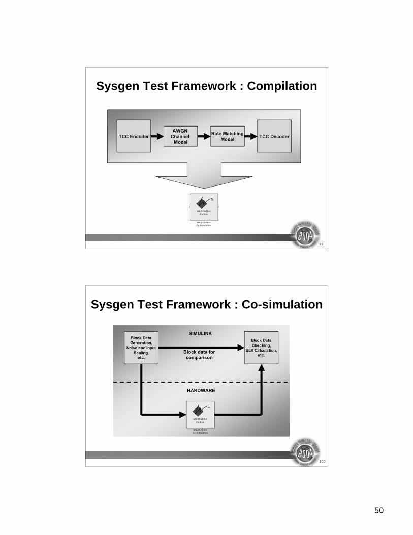
Sysgen Test Framework : Compilation
TCC Encoder TCC Decoder
AWGN
Channel
Model
Rate Matching
Model
100
Sysgen Test Framework : Co-simulation
Block Data
Generation,
Noise and Input
Scaling,
etc.
Block Data
Checking,
BER Calculation,
etc.
SIMULINK
HARDWARE
Block data for
comparison
51
101
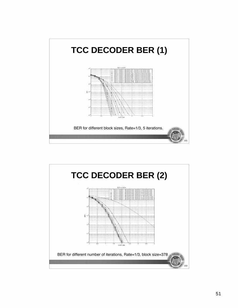
TCC DECODER BER (1)
BER for different block sizes, Rate=1/3, 5 iterations.
102
TCC DECODER BER (2)
BER for different number of iterations, Rate=1/3, block size=378
52
103
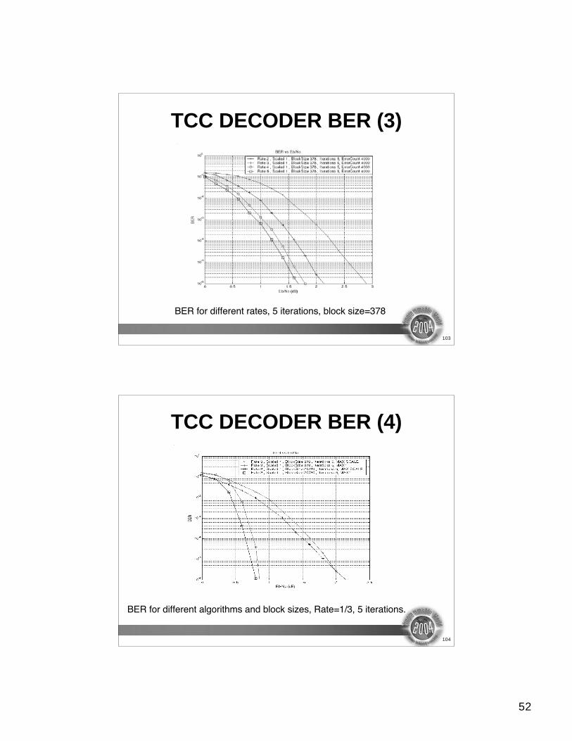
TCC DECODER BER (3)
BER for different rates, 5 iterations, block size=378
104
TCC DECODER BER (4)
BER for different algorithms and block sizes, Rate=1/3, 5 iterations.
53
105
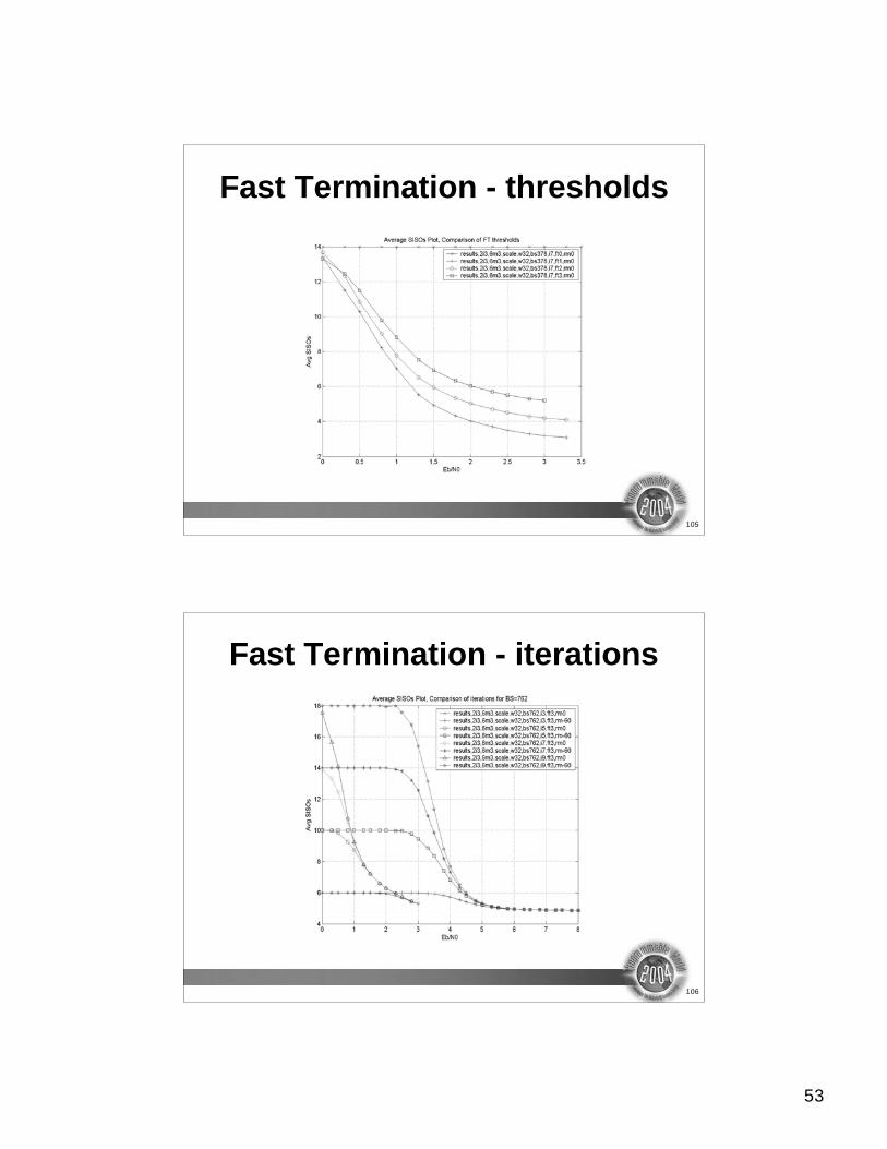
Fast Termination - thresholds
106
Fast Termination - iterations
54
107
Agenda• Next generation wireless systems: 4G technologies
• FPGAs and the wireless PHY– Modulation
• Multicarrier (OFDM) systems
– Symbol rate processing• Channel coding for OFDM (COFDM) and UMTS/CDMA2000
systems
– IF processing• Digital pre-distortion
• Conclusion
108
PA Linearization (1)• PA linearization is a key aspect to reducing system cost
• Analog processing is one possibility
• Digital baseband pre-distortion (DPD) is preferred
• Large processing requirements for wide BW
Modem Pre-Distorter DAC PARF
Down
ConvertADC
Adaptive
Processing
FPGA
55
109
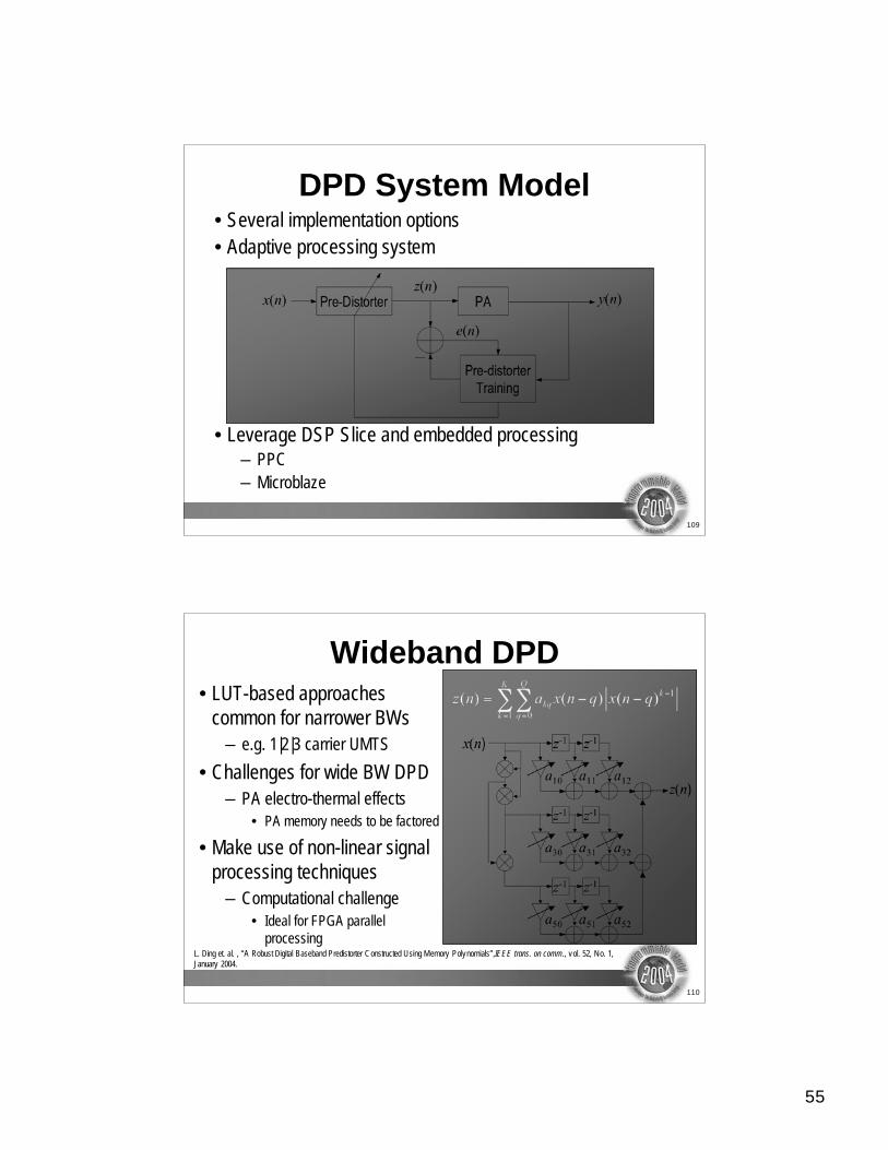
DPD System Model• Several implementation options
• Adaptive processing system
• Leverage DSP Slice and embedded processing– PPC
– Microblaze
Pre-Distorter
Pre-distorter
Training
PAx(n) y(n)z(n)
e(n)
110
Wideband DPD• LUT-based approaches
common for narrower BWs
– e.g. 1|2|3 carrier UMTS
• Challenges for wide BW DPD
– PA electro-thermal effects
• PA memory needs to be factored
• Make use of non-linear signal
processing techniques
– Computational challenge
• Ideal for FPGA parallel
processing
z-1 z-1
a10 a11 a12
z-1 z-1
a30 a31 a32
z-1 z-1
a50 a51 a52
x(n)
z(n)
L. Ding et. al. , “A Robust Digital Baseband Predistorter Constructed Using Memory Polynomials” ,IEEE trans. on comm., vol. 52, No. 1,
January 2004.
56
111
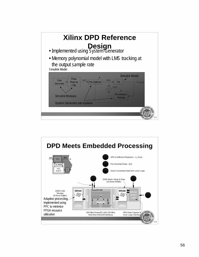
Xilinx DPD Reference
Design• Implemented using System Generator
• Memory polynomial model with LMS tracking at
the output sample rate
Pre-Distorter
Pre-distorter
Training
PAx(n)
y(n)z(n)
e(n)
Data
Generator
Pulse
Shaping
Filter
Simulink Modules
Simulink Model
System Generator sub-systems
Simulink Model
112
DPD Meets Embedded Processing
1
BRAMSelectLogic
PowerPC 405
ISO
CM
DS
OC
M
BRAM
JTAG Reset
BRAM
x(n) z(n)~
a_rls(n)
VPD
PPCSystem
U
2
3
VPD Coefficient Registers - a_rls(n)1
Pre-Distorted Data - (n)2
Down Converted Data from User Logic3
16kB CodeStorage
(8 block RAMs)
Data Control RegisterBus (32-bit @ 100 MHz)
32kB Stack, Heap & Data(16 block RAMs)
300 MHz PowerPC with 150 MHz ISOCM & DSOCM Interfaces
VPD Data Capture &User Logic Interface
Adaptive processing
implemented using
PPC to minimize
FPGA resource
utilization
57
113
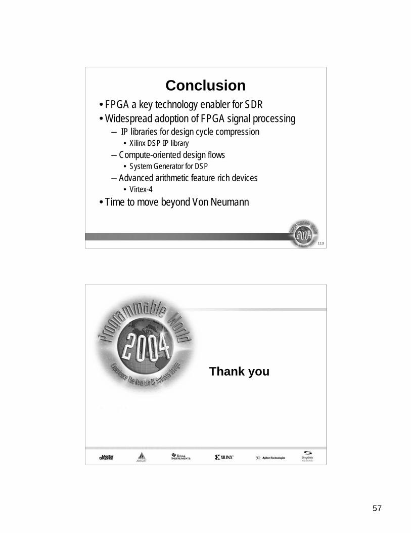
Conclusion
• FPGA a key technology enabler for SDR
• Widespread adoption of FPGA signal processing
– IP libraries for design cycle compression• Xilinx DSP IP library
– Compute-oriented design flows• System Generator for DSP
– Advanced arithmetic feature rich devices• Virtex-4
• Time to move beyond Von Neumann
Thank you


![Solutions Enabler 8.1 Installation Guide - Dell EMC · 2 Solutions Enabler 8.1 Installation Guide. 13 15 ... [GA] - x86_64 ... Solutions Enabler 8.1 Installation Guide 9.](https://static.fdocuments.in/doc/165x107/5b805fa37f8b9ad4778d4e79/solutions-enabler-81-installation-guide-dell-emc-2-solutions-enabler-81.jpg)


