Solutions for Designing High-Speed Systemsactel.kr/_exhibit/2003/4_High_Speed.pdf · 5 History of...
63
Transcript of Solutions for Designing High-Speed Systemsactel.kr/_exhibit/2003/4_High_Speed.pdf · 5 History of...


Solutions for Designing High-Speed SystemsSolutions for Designing High-Speed Systems

3
AgendaAgendaEvolution of Data CommunicationsData Integrity ChallengesSignal Integrity & Board Design Challenges

4
History of CommunicationsHistory of Communications

5
History of CommunicationsHistory of Communications
Central Office
More Efficient Networks− Dramatically Reduces Number of Point-to-Point
ConnectionsCentral OfficeSerialized Data
6
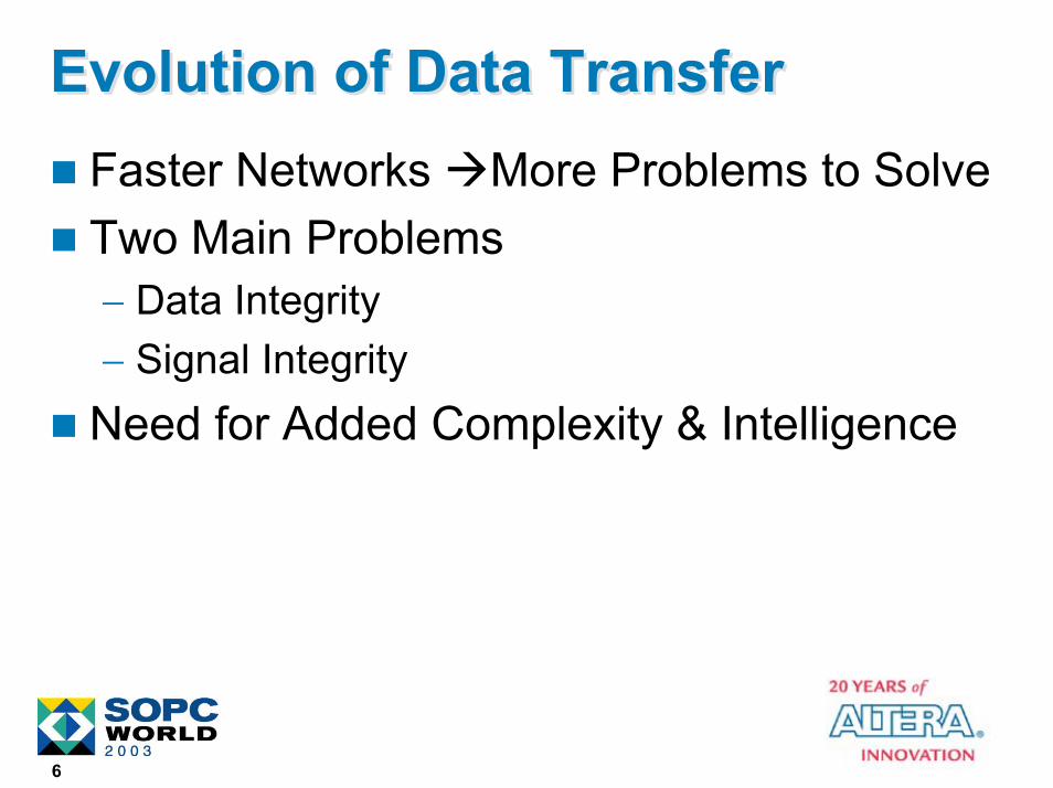
Evolution of Data TransferEvolution of Data TransferFaster Networks More Problems to SolveTwo Main Problems− Data Integrity− Signal Integrity
Need for Added Complexity & Intelligence

7
Datacom StandardsDatacom StandardsEvolution of Datacom Standards− ATM, Ethernet
Ethernet: the Choice for 70% of Data Networks− First Developed in 1973 by DEC, Intel & Xerox− 10Base-T: 10 Mbps− 100Base-T: 100 Mbps (Fast Ethernet)− 1000Base-T: 1 Gbps (Gig-E)
Gigabit Ethernet: Uses 4 Pairs of Twisted Pair at 250 Mbps10 Gigabit Ethernet (XAUI): Uses 4 Pairs at 3.125 Gbps

8
Why Serial Data? Why Everywhere?Why Serial Data? Why Everywhere?
Parallel Data Worked for Short Distances & Low Clock Rates− Skew & Timing Budget− Signal Count, Power, Connector Size, Pin
Count, EMC Issues PCB Real Estate (Can’t Just Go Wider)Parallel Data Buses Are EXPENSIVE!!Serialization Solves Most of These Problems

9
TrendsTrendsCommunication
50 cm7 cmTotal Reach
1674Total Pins/PairControl ChannelsClock ChannelsData Channels
I/O Standard
0401
4 Differential32
DifferentialHSTL 1 S.E.
XAUIXGMII
Computers
2.5 Gbps33 Mbps
PCI ExpressPCI
3.125 Gbps800 Mbps
SerialRapidIO
ParallelRapidIO
Industrial

10
Data IntegrityData IntegrityAdded Overhead in the Data Stream− Clock & Data Recovery− Initialization of the Link− Data Encoding/Decoding− Word Boundary− Skew Compensation, Clock Domain
Decoupling− Error Checking/Recovery
Consider XAUI

11
XAUI Data ManagementXAUI Data ManagementEncode XGMII into 10 Bits/Lane At 3.125 GbpsSynchronization of Code Groups on Each Lane− Word Alignment ||K||
Deskew of Received Code Groups across Lanes− Channel Aligner ||A||
Clock Decoupling Across Domains− Rate Matching ||R||
Conversion of XGMII Idle Control Characters to a Random Sequence of XAUI Control Characters

12
XAUI Implementation in Stratix GXXAUI Implementation in Stratix GX
ReceiveTransmit
Serial-to-Parallel
ClockRecovery
Unit
Rx PLLReferenceClock
Tx PLL
Parallel-to-Serial 8B/10B
EncoderSynch-ronizer
ReferenceClock
PatternDetector& WordAligner
8B/10BDecoder
Synch-ronizer
RateMatcher
&ChannelAligner
Recovered Clock to Core
12

13
Slave 2Slave 2TXTX
RXRX
Slave 3Slave 3
RXRXTXTX
Slave 1
TXRX
MasterMaster
TX
RXRXLink
LayerLink
Layer
Case Study 1: Medical InstrumentationCase Study 1: Medical Instrumentation

14
Case Study 1: Medical InstrumentationCase Study 1: Medical Instrumentation
Network of Medical Instruments in a Building− Master Slave Configuration, Ring Structure− Slave Instruments Transfer Data to Master
Analysis Center− Data Transfer at 3.125 Gbps− 2 Redundant Channels

15
Case Study 1: RequirementsCase Study 1: RequirementsData Flows in One DirectionSimple Flow Control & Initialization− Asynchronous System− Not Too Concerned about Dropped Packets
Initialization− Master Sends Beacon Containing Address of
Slave of Interest + ||XXXXX||− Once Link Initializes, Data Transfer Starts− Re-Initialize in Event of Failure

16
Case Study 1: ImplementationCase Study 1: ImplementationUtilizes Stratix™ GX Device’s Built-In XAUI Hard IP − Word Align, Channel Align, Rate Match, 8B10B
Coding & Phase Compensation FIFOUse of a Simple ProtocolLink Layer Implemented in the FPGA Logic Array of Master NodeNon XAUI Network, But Uses the Built-in XAUI Hard IP

17
Case Study 2: Semiconductor Test EquipmentCase Study 2: Semiconductor Test Equipment
Point-to-Point Communication− 2.5 Gbps Serial Data Rate across Backplane− Efficient Data Transfer: Low Latency, Low
Overhead− Does Not Need Quad-Based Data Transfer− Cannot Use A Heavy Protocol

18
Case Study 2 : ImplementationCase Study 2 : Implementation
LiteLink Layer
+Rate
Matching
FPGALogicArray
8B/10BDecoder
Phase CompFIFO
8B/10BEncoder
SerializerRetimer
PhaseCompFIFO
CDRDeserializer
BackplaneInterface

19
Case Study 2: ImplementationCase Study 2: ImplementationMost of the XAUI Hard IP Not Necessary or Applicable− Rate Matching Implemented in the FPGA
Logic ArrayLight Link Layer Incorporated in FPGA Logic Array− Cut-through Mode, CRC, Error Recovery
Leverages Flexibility of FPGA Solution!

20
XAUI ProtocolXAUI ProtocolXAUI : 4 Lanes of Traffic Overhead− Synchronization− Channel to Channel Skew− Rate Matching− Initialization
Very Heavy Protocol (Lots of LEs)

21
Simple Serial Link ApplicationsSimple Serial Link ApplicationsPacket or Streaming DataChip-to-Chip ConnectivityBoard-to-Board ConnectivityShelf-to-Shelf ConnectivityBackplane CommunicationOptical Connectivity
Atlantic™StreamingInterface Tr
ans c
eive
rs
Use
r
Payl
oad
Ligh
tweig
ht
Prot
ocol
Stratix GX
User Device
Tran
s cei
vers
Ligh
tweig
ht
Prot
ocol
Use
r
Payl
oad
StreamingInterface
One or More Channels
22
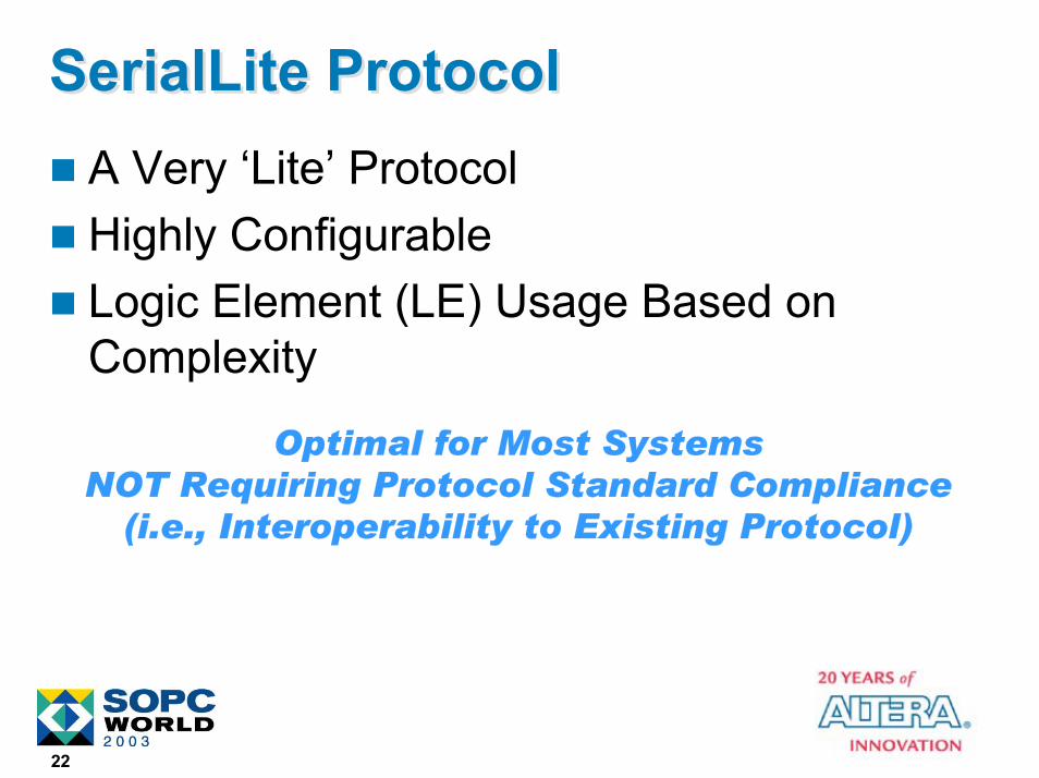
SerialLite ProtocolSerialLite ProtocolA Very ‘Lite’ ProtocolHighly ConfigurableLogic Element (LE) Usage Based on Complexity
Optimal for Most SystemsNOT Requiring Protocol Standard Compliance
(i.e., Interoperability to Existing Protocol)
23
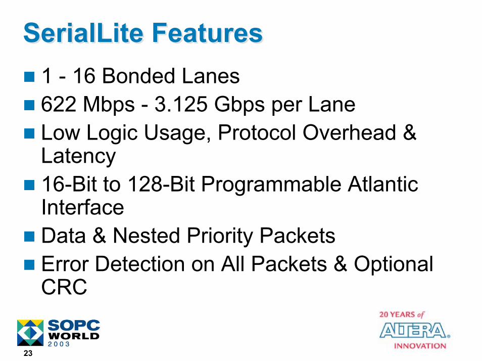
SerialLite FeaturesSerialLite Features1 - 16 Bonded Lanes622 Mbps - 3.125 Gbps per LaneLow Logic Usage, Protocol Overhead & Latency16-Bit to 128-Bit Programmable Atlantic InterfaceData & Nested Priority PacketsError Detection on All Packets & Optional CRC

24
SerialLite ProtocolSerialLite ProtocolAvailability− Single Lane Version: December 2003− Multi-Lane Complete Package: May 2004
Open Standard: Freely Available for Everybody to UseSpecification Available Today, Contact Altera Sales Representative for Details

Signal IntegritySignal Integrity

26
Eye DiagramEye DiagramWaveform Represents a Logical ‘1’
Waveform Represents a Logical ‘0’
Ideal Eye Diagram with No Noise
Eye Diagram with Voltage Noise
Eye Diagram with Timing Noise
Eye Diagram with Voltage & Timing Noise
27
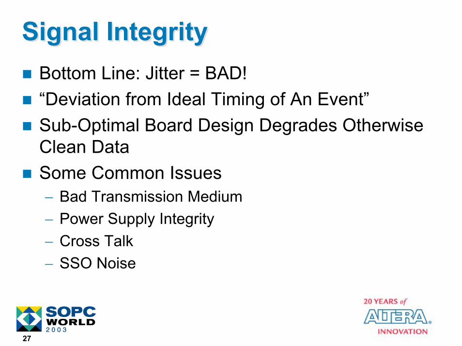
Signal IntegritySignal IntegrityBottom Line: Jitter = BAD!“Deviation from Ideal Timing of An Event”Sub-Optimal Board Design Degrades Otherwise Clean DataSome Common Issues− Bad Transmission Medium− Power Supply Integrity− Cross Talk− SSO Noise

28
Jitter ComponentsJitter ComponentsTwo Kinds of Jitter− Deterministic & Random
Total Jitter Constituents
Total Jitter
Deterministic Jitter Random Jitter
Sinusoidal Jitter Data Dependent Jitter
Duty Cycle DistortionInter-Symbol Interference
Uncorrelated Jitter
29
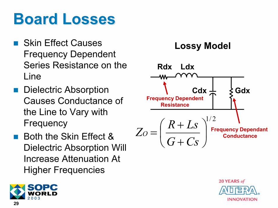
Board LossesBoard LossesSkin Effect Causes Frequency Dependent Series Resistance on the Line Dielectric Absorption Causes Conductance of the Line to Vary with FrequencyBoth the Skin Effect & Dielectric Absorption Will Increase Attenuation At Higher Frequencies
Lossy Model
Rdx Ldx
Cdx Gdx
2/1
++
=CsGLsRZO
Frequency DependentResistance
Frequency Dependant Conductance

30
Skin EffectSkin EffectHigh Frequency Current Flows Primarily on the Surface of A ConductorChanging Current Distribution Causes Resistance to Increase As Function of Frequency
Cross Sectional View
Stripline Trace
(Skin Depth)δGroundPlane
Dielectric
Current Path
µπρδF
= Resistivity
Permeability of Free Space
Frequency

31
Dielectric AbsorptionDielectric AbsorptionHigh Frequency Signals Excite Molecules in the Insulator− Insulator Absorbs Some of the Signal’s Kinetic Energy− Signal’s Magnitude Is Attenuated
Dielectric Absorption Often Specified in Terms of Loss Tangent, tan(δ)Lower tan(δ) = Less Losses
3.05
3.64.004.05
0.004
0.0090.0150.020
tan(δ) at 1 GHz
ARLON CLTE
Rogers 4350/4320
GETEKFR4
Material
6.83.15
2.13.751.14.151.04.30
Relative Costεr at 1MHz εr at 1GHz

32
Inter-Symbol Interference (ISI)Inter-Symbol Interference (ISI)Residual Voltages on Transmission Line that Can Interfere with Signals Traveling At Later Time− Reflections Off Impedance Discontinuities in the
Transmission Line− Resonant Transmitter (LC Tank Circuit)− Inertial Delay & Hidden State (RC Circuit)
ISI Degrades Signal Integrity of Transmission Line − Closes the Eye

33
Example Eye DiagramsExample Eye Diagrams
Eye Diagrams after 2”, 22” & 36” of Backplane
Eye after 2” of FR4Eye after 22” of FR4Eye after 36” of FR4

34
What Can We Do About it?What Can We Do About it?Programmable Pre-Emphasis!Boost High-Frequency Components to Reduce PDJ − When Switching Occurs the Differential Drive Is Increased− 6 Settings from 0% to 140% Based on vOD Setting
vOD(P-P)High Freq.
Six Programmable Settings
vOD(P-P)Low Freq.
Six Programmable SettingsUI UI

35
Pre-Emphasis Opens the EyePre-Emphasis Opens the Eye
Pre-Emphasis Setting = 0Pre-Emphasis Setting = 1Pre-Emphasis Setting = 2Pre-Emphasis Setting = 3Pre-Emphasis Setting = 4
40” BackplanevOD of 400 mV
Near End Far End
36
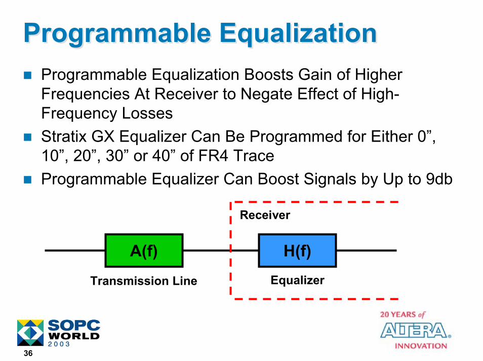
Programmable EqualizationProgrammable EqualizationProgrammable Equalization Boosts Gain of Higher Frequencies At Receiver to Negate Effect of High-Frequency Losses Stratix GX Equalizer Can Be Programmed for Either 0”, 10”, 20”, 30” or 40” of FR4 TraceProgrammable Equalizer Can Boost Signals by Up to 9db
Receiver
A(f) H(f)EqualizerTransmission Line

37
Equalizer Frequency ResponseEqualizer Frequency Response
Equalizer
Equalizer+T-Line
T-Line

38
Equalizer Opens the EyeEqualizer Opens the Eye40” BackplanevOD of 400 mVEqualizer Setting = 0Equalizer Setting = 10”Equalizer Setting = 20”Equalizer Setting = 30”Equalizer Setting = 40”
Near End Far End200 mV
0 mV
-200 mV
100 mV
-100 mV

39
Effects of Improper TerminationEffects of Improper TerminationThe Ratio of Reflected Voltage Amplitude to the Incident Voltage Amplitude Defined As Reflection Coefficient, (Kr):
In General, Kr Is Determined by Telegrapher’s Equation
OT
OT
I
Rr
ZZZZ
VVk
+−
==
Vs
Zs
ZTZO ,TPD

40
Programmable On-Chip TerminationProgrammable On-Chip TerminationStratix GX Devices Offer Differential Programmable Termination of 100, 120, 150 Ohms for Both Receivers & TransmittersTermination for Channels Can Be Chosen IndependentlyTx & Rx Termination on Same Channel Chosen Independently

41
Programmable Drive Strength Programmable Drive Strength Programmable VOD(p-p) Settings from 400 to 1,600 mV
Programmed Output Current (mA)
4
8
10
12
14
16
VOD(p-p)at 100 Ω
400
800
1,000
1,200
1,400
1,600
VOD(p-p)at 120 Ω
480
960
1,200
1,440
-
-
VOD(p-p)at 150 Ω
600
1,200
1,500
-
-
-
Board Design IssuesBoard Design Issues

43
Board DesignBoard DesignNot Your Average Low-Speed BoardVery Observable Cause & EffectsHigh-Speed Line Routing Return Paths Decoupling of Power Supply NoiseLayer Stackup & Spacing

Board LayerStackupBoard LayerStackup
Bottom Signal (50 ohm)18
Power17
Signal (50 ohm)16
High-Speed Signal (100 Ohm)15
High-Speed GND14
High-Speed Signal (100 Ohm)13
Signal (50 Ohm)12
Power11
Signal (50 Ohm)10
Signal (50 Ohm)9
PLL GND8
Signal (50 Ohm)7
Signal (50 Ohm)6
Power5
Signal (50 Ohm)4
Signal (50 Ohm)3
GND2
Top Signal (50 Ohm)1
Layer TypeLayer Number
44

45
High-Speed Transmission LinesHigh-Speed Transmission LinesSeamless Data Transfer: 50 Ohm EnvironmentRemember Telegrapher’s Equation?
OT
OT
I
Rr
ZZZZ
VVk
+−
==

46
DiscontinuitiesDiscontinuitiesWhen Dealing with Discontinuities on the Board, Consider the Following Factors− Right-Angle Bends− Vias− Connectors− Improper Terminations

47
ViasVias
Stub
Things to Worry about− Stub Is Created At the Via− Effect of Stubs:
Inductance Is Small. Flux Lines Cancel At End of Via Due to the Whole Signal Reflecting
− An Inductive Discontinuity Is Created on the Line Due to Improper Return Paths

48
ViasViasCannot Avoid Vias− Routing Issues− Impedance Control on Top Layer
Use As Much of the Via As Possible to Reduce StubBack Drill or Blind Vias to Eliminate Stub, But ExpensiveGround Vias around Signal Via, Control InductanceFor 3.125-Gbps Signal Board Thicknesses of 150 Mils & above, Vias Play Big Role

49
ConnectorsConnectorsConnectors on Transmission Paths Are Discontinuities− Based on Type of Connector They Can Be Either
Capacitive or Inductive DiscontinuityCapacitive Dip Due to Connector
Capacitive Dip Due to Via

50
DecouplingDecouplingResonant Tanks Due to Parasitic ImpedancesSpikes Caused by Data Edges Induce Oscillations in Power Supply Voltages− Oscillations Over a Range
of Frequencies
Noisy Power Supply => Increased Jitter
Stratix GX Eyewith Poor Decoupling

51
DecouplingDecouplingNeed to Filter Out the Noise Using Bypass Capacitors− Use a Range of Capacitance Values to Cover
Frequency Range ( Example: 0.01 µF to 200 µF)Increasing Influence of Parasitic Inductance with FrequencyNeed for Power-Ground Plane Capacitance− Capacitance Due to Parallel Plate Capacitance − Minimal Parasitic Resistance & Inductance
Parallel Plate Capacitance = εoεr (A/d)

52
Decoupling RecommendationsDecoupling RecommendationsStratix GX Eye with Poor
Decoupling
Stratix GX Eye with Effective
DecouplingLocate the High Frequency Decoupling Capacitors As Close to the IC As PossibleBulk Capacitors Can be Placed Farther AwayUse Power – Ground Plane Capacitors As Much As PossibleUse Low Inductance Capacitors
53
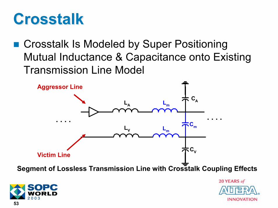
CrosstalkCrosstalkCrosstalk Is Modeled by Super Positioning Mutual Inductance & Capacitance onto Existing Transmission Line Model
LA Lm
LV
CA
Cm
CV
Lm
Aggressor Line
Victim Line
. . . .. . . .
Segment of Lossless Transmission Line with Crosstalk Coupling Effects

54
Crosstalk & TerminationCrosstalk & TerminationHow Can You Reduce Noise Caused By Crosstalk?− Crosstalk Is A Proportional Noise Source, So Increasing the
Signal Swing Will Only Increase Amount of Coupling Noise− Both Near-End & Far-End of Line Needs to Be Terminated to
Reduce Noise Caused By Crosstalk− Lines Spaced Sufficiently Apart; EM Simulations
What to do?

55
SSO NoiseSSO NoiseDrivers Switch High to Low− Ground Bounce Occurs− Also Power Collapse Occurs
Higher the Inductance, Higher the G B Voltage (V = L (di/dt))Higher the Inductance, More the Power Collapses More I/O Switching Requires More Regional Energy
Load Capacitance
Loop
L1
L2
Vcc

56
How to Reduce SSO Noise?How to Reduce SSO Noise?Spread Out I/O Pins Being Used− Use Different Power Pins
Use Differential Signaling Rejects Common Mode NoiseSlow Down the Slew Rate of Driver (dI/dt)− This Reduces V = L (dI/dt)
Use Programmable Grounds/ Supply− Tie Unused I/O Pins to Ground / VDD

57
Stratix GX Applications BoardStratix GX Applications BoardEthernet& RS232 Power
Circuitry
DDR SDRAMDIMM
SPI-4 HmZd Interfaceto Backplane
XPAK Stratix GX Device
SFPXCVR SMA

58
Signal Integrity Simulation ToolsSignal Integrity Simulation ToolsChip-Level Simulations HSPICEHSPICE Still the Most Reliable High-Speed SimulatorNeed to Accurately Model the Transmission Medium− Transmission Lines, Vias, Connectors− RLGC Parameters Imported to HSPICEPkg
ModelT-Line Cable Line card Con. Bkpln Con. Line card Cable outa
outbSMA

59
Signal Integrity SimulationsSignal Integrity SimulationsEM Field Solvers Used to Extract Board ModelsAssign Conductor & Dielectric MaterialsSetup Solution Parameters − Inductance, Capacitance, Impedance & Admittance
Solve ParametersCheck Solution for Various Parameters− Characteristic Impedance, RLGC Values, Propagation
Delay, Crosstalk, Skin Effect

60
Simulation Vs. MeasurementSimulation Vs. MeasurementConditions: Stratix GX Device Driving 20” of XAUI Backplane (Connectors & Daughter Card Included)
Simulation Measurement

61
Altera’s Support StructureAltera’s Support StructureAltera Provides Simulation Models− HSPICE, VHDL AMS, DML (Soon)
Board Layout Guidelines with Sample LayoutCharacterization ReportsComplete User GuideHigh-Speed Expert Customer Support

62
SummarySummarySerial Communication Is the New StandardMany Protocols Available to Implement SystemPre-Emphasis & Equalization Make Huge ImpactCareful Design of Board for High-Speed Signaling Is CriticalMany Tools Available to Ensure Successful Design Implementation