The effect of atomic density gradient in electromigration
18
36 Int. J. Materials and Structural Integrity, Vol. 6, No. 1, 2012 Copyright © 2012 Inderscience Enterprises Ltd. The effect of atomic density gradient in electromigration Yuanxiang Zhang* College of Mechanical Engineering, Quzhou University, Quzhou 324000, China E-mail: [email protected] *Corresponding author Yong Liu Fairchild Semiconductor Corp., 82 Running Hill Road, South Portland, ME 04106, USA E-mail: [email protected] Lihua Liang Fairchild-ZJUT Microelectronic Packaging Joint Lab, Zhejiang University of Technology, Hangzhou 310014, China E-mail: [email protected] Xuejun Fan Department of Mechanical Engineering, Lamar University, Beaumont, TX 77705, USA E-mail: [email protected] Abstract: This paper studies the electromigration (EM) failure of interconnect structure and solder joint in a wafer level chip scale package (WL-CSP) based on atomic flux divergence (AFD) method. The impact of atomic density gradient (ADG) on the divergence of the atomic fluxes is investigated. The simulation results show that the traditional AFD method, which neglects the effect of atomic density gradient, can result in significant errors in predicting solder joint failures in a WL-CSP; while the AFD method with the consideration of the atomic density gradient has shown more reasonable results. Keywords: electromigration; EM; atomic density gradient; ADG; interconnects; solder joints; atomic flux divergence; AFD; wafer level chip scale package; WL-CSP. Reference to this paper should be made as follows: Zhang, Y., Liu, Y., Liang, L. and Fan, X. (2012) ‘The effect of atomic density gradient in electromigration’, Int. J. Materials and Structural Integrity, Vol. 6, No. 1, pp.36–53.
Transcript of The effect of atomic density gradient in electromigration

36 Int. J. Materials and Structural Integrity, Vol. 6, No. 1, 2012
Copyright © 2012 Inderscience Enterprises Ltd.
The effect of atomic density gradient in electromigration
Yuanxiang Zhang* College of Mechanical Engineering, Quzhou University, Quzhou 324000, China E-mail: [email protected] *Corresponding author
Yong Liu Fairchild Semiconductor Corp., 82 Running Hill Road, South Portland, ME 04106, USA E-mail: [email protected]
Lihua Liang Fairchild-ZJUT Microelectronic Packaging Joint Lab, Zhejiang University of Technology, Hangzhou 310014, China E-mail: [email protected]
Xuejun Fan Department of Mechanical Engineering, Lamar University, Beaumont, TX 77705, USA E-mail: [email protected]
Abstract: This paper studies the electromigration (EM) failure of interconnect structure and solder joint in a wafer level chip scale package (WL-CSP) based on atomic flux divergence (AFD) method. The impact of atomic density gradient (ADG) on the divergence of the atomic fluxes is investigated. The simulation results show that the traditional AFD method, which neglects the effect of atomic density gradient, can result in significant errors in predicting solder joint failures in a WL-CSP; while the AFD method with the consideration of the atomic density gradient has shown more reasonable results.
Keywords: electromigration; EM; atomic density gradient; ADG; interconnects; solder joints; atomic flux divergence; AFD; wafer level chip scale package; WL-CSP.
Reference to this paper should be made as follows: Zhang, Y., Liu, Y., Liang, L. and Fan, X. (2012) ‘The effect of atomic density gradient in electromigration’, Int. J. Materials and Structural Integrity, Vol. 6, No. 1, pp.36–53.

The effect of atomic density gradient in electromigration 37
Biographical notes: Yuanxiang Zhang is currently a Lecturer in the College of Mechanical Engineering, Quzhou University. He received his BS in Mechanical Engineering, MS in Solid Mechanics and PhD in Electronics Packaging at Zhejiang University of Technology, Hangzhou, China, in 2005, 2008 and 2011, respectively. He has published more than ten research papers in international and national journals and conferences. His research interests include the electronic package thermal, moisture analysis and electromigration simulations in electronic devices.
Yong Liu received his BS in Mechatronics, and MS and PhD in Mechanical Engineering from Nanjing University of Science and Technology, Nanjing, China, in 1983, 1987, and 1990, respectively. He is currently a senior member of Technical Staff at Fairchild Semiconductor Corporation, South Portland, ME. He has co-authored over 150 papers in journals and conferences, two books, and has filed over 40 US patents in the area of analogue and power electronic packaging. His research interests are advanced IC packaging, modelling and simulation, reliability, and material characterisation.
Lihua Liang received his BS and MS in Mechanical Engineering from Zhejiang University of Technology in 1995 and 1998, respectively, and a PhD in Solid Mechanics from Zhejiang University, in 2006. He is currently a Professor in the College of Mechanical Engineering, Zhejiang University of Technology. His research interests include computational mechanics and reliability of microelectronic packages.
Xuejun Fan received his BS and MS from Tianjin University, Tianjin, China in 1984 and 1986, respectively, and a PhD in Engineering Mechanics from Tsinghua University, Beijing, China, in 1989. He is currently an Associate Professor in the Department of Mechanical Engineering, Lamar University, Beaumont, TX. He has published more than 100 scientific papers, two books and filed five US patents. His interests and expertise lie in the areas of reliability, material characterisation and thermal and mechanical modelling for microelectronic packaging.
1 Introduction
Electromigration (EM) is a phenomenon of mass transport in metallisation structures when a high electrical current density is applied. It can cause progressive damage to metal interconnect in an integrated circuit (IC). Usually, voids nucleation near cathode side and hillock development near anode side during current stressing indicate a biased mass diffusion from cathode to anode. As the electronics industry continues to push for higher performance and miniaturisation, the demands of higher current densities increases. This may cause EM failures, not only in IC interconnects but also in solder bumps of IC packages.
In recent years, there are a lot of efforts attempting to predict the EM failure through modelling. Dalleau and Weide-Zaage (2001) provided a 3D EM modelling using the finite element analysis (FEA) based on the traditional atomic flux divergence (AFD) method. The migration driving forces they considered are the electron-wind force induced migration (EWM), the temperature gradient induced migration (TM) and the stress gradient induced migration (SM). Later on, there are other researches on the AFD method (Sasagawa et al., 2002; Sukharev and Zschech, 2004). Tan et al. (2007) indicated

38 Y. Zhang et al.
that the traditional AFD formulation is not accurate in predicting void nucleation sites in a very thin film structure. Therefore, they proposed a modified AFD formulation by introducing a volume-averaged stress concept for investigating the void nucleation sites and the void growth process in copper dual damascene interconnects. In addition, Li et al. (2008) and Li and Basaran (2009) proposed a model for simulating the damage mechanics of EM and TM and their interaction. The governing equations utilised for the model include mass conservation, force equilibrium, heat transfer and electricity conduction.
In reality, the atomic mass transport is caused by a combination of interacting driving forces, which can generate voids at different locations. These driving forces are induced from different physical phenomena such as momentum exchange with current carriers (electron wind), temperature gradients, mechanical stress gradients, and atomic density gradient (ADG) (or more general, of the chemical potential) (Tan and Roy, 2006; Liu et al., 2010). However, the traditional AFD method neglects the effect of the ADG. We need to find out what would be the impact on the fundamental mechanism of the EM if the ADG is neglected and how significant the effect of the ADG would be in both interconnects and solder joint system of a wafer level chip scale package (WL-CSP). In this paper, we will investigate the AFD method and the impact of the ADG on the divergences of the atomic fluxes. The comparison of results with and without considering the ADG is discussed in details.
2 AFD method
To simplify the problem, only the electron wind, temperature gradients and ADGs are considered in this work. Therefore, the atomic flux due to the three above driving forces can be expressed as following (Sukharev and Zschech, 2004):
*A
cDJ Z e jkT
ρ= (1a)
*Th
cD TJ QkT T
∇= − (1b)
CJ D c= − ∇ (1c)
In the above, c is the normalised atomic density, c = N / N0, N is the current atomic density and N0 is the initial (equilibrium state) atomic density; k is the Boltzmann’s constant; e is the electronic charge; Z* is the effective charge which is determined experimentally; T is the absolute temperature; ρ is the resistivity which is calculated as ρ = ρ0(1 + α(T – T0)), where α is the temperature coefficient of the metallic material, ρ0 is the resistivity at T0; j is the current density vector; Q* is the heat of transport;
0exp aED D
kT⎛ ⎞= −⎜ ⎟⎝ ⎠
is the effective atom diffusivity, where Ea is the activation energy, D0
is the effective thermally activated diffusion coefficient.

The effect of atomic density gradient in electromigration 39
From the atomic flux equation (1a) to equation (1c), the divergence of the respective atomic fluxes can be derived as
( ) 01 1div aA A A
EJ J T J c
kT T cρ
αρ
⎛ ⎞′ = − + ⋅ ⋅∇ + ⋅∇⎜ ⎟⎝ ⎠
(2a)
( )*
2 2 202 3 3
3 1div3
aTh Th Th
E cQ DJ J T j e J cT ckT k T
ρα ρ
ρ⎛ ⎞′ = − + ⋅ ⋅∇ + + ⋅∇⎜ ⎟⎝ ⎠
(2b)
( )div div( )aC C
E TJ J D ckT T
∇′ = ⋅ ⋅ − ⋅ ∇ (2c)
( ) ( ) ( ) ( )div div div divTotal A Th CJ J J J′ ′ ′′= + + (2d)
Based on the mass balance mechanism, the time dependent evolution equation of a local atomic density can be written as:
( )div 0TotalcJt∂′ + =∂
(3)
In conventional AFD method (Dalleau and Weide-Zaage, 2001; Tan et al., 2007), the effect of ADG ∇c is neglected. Therefore, the divergences of atomic flux for EM and thermomigration can be expressed as below:
( ) 01div aA A
EJ J T
kT Tρ
αρ
⎛ ⎞′′ = − + ⋅ ⋅∇⎜ ⎟⎝ ⎠
(4a)
( )*
2 2 202 3 3
3div3
aTh Th
E cQ DJ J T j eTkT k T
ρα ρ
ρ⎛ ⎞′′ = − + ⋅ ⋅∇ +⎜ ⎟⎝ ⎠
(4b)
( ) ( ) ( )div div divTotal Total ThJ J J′′ ′′ ′′= + (4c)
Without consideration of the ADG, the total atomic divergence equation (4c) consists of electron wind divergence and thermal migration divergence. Equation (3) can be solved by direct integral method.
Recently, Liu et al. (2010) developed a method for prediction of voids in EM. This method solves the mass balance equation (3) for atomic density with blocking boundary condition based on the weighted residual finite element. The new method avoids directly solving the divergences of the atomic flux, which is very hard to get the solution by traditional method. Thus, after we get the atomic density distribution through the new method, then the divergences of atomic flux due to electron wind, temperature gradients and ADG by equation (2a) and equation (2c) can then be investigated easily.

40 Y. Zhang et al.
3 AFD investigation, comparison and discussion
3.1 A wafer level interconnect structure
A standard wafer level electromigration accelerated test (SWEAT) structure (Dalleau, 2003) is selected for the examination (see Figure 1). The aluminium alloy (with 1% Si) is 0.88 μm thick. The radius at the corner is 1 μm. The width of aluminium line is 2 μm. The length of the inner metal line of the structure is 10 μm. To simplify the model, the thickness of the silicon substrate is taken to be 5 μm. Due to the symmetry of the SWEAT, only a half of the structure is modelled.
Figure 1 SWEAT structure and its mesh (see online version for colours)
Al (%1Si) alloy
Si
SiO2
Electron flow
Cathode
Anode
The material and EM parameters used in this paper are shown in Tables 1 and 2, which are from Dalleau (2003), Liu et al. (2010) and Jeon and Park (2004). Table 1 Material properties of the SWEAT
Materials Elastic
modulus (GPa)
Poisson’s ratio
Thermal conductivity
(W/mK) Electrical resistivity (Ω·m)
Al 69 0.35 240 3.24E-8(1 + 3.51E-3(T – 303)) SiO2 71 0.16 1.75 1E10 Si 130 0.28 80 4.4
CTE (ppm/K) Materials
200K 300K 400K 500K 600K 700K 800K Al 20.3 23.23 25.1 26.4 28.4 30.9 34 SiO2 0.348 0.498 0.61 0.63 0.59 0.53 0.47 Si 2.24 2.64 3.2 3.5 3.7 3.9 4.1

The effect of atomic density gradient in electromigration 41
Table 2 EM parameters of Al (1%Si)
Parameters Symbol Unit Value
Activation energy Ea eV 0.87 Effective charge number Z* - –4 Self-diffusion-coefficient D0 m2/s 5E-8 Heat of transport Q* eV –0.0867 Atomic volume Ω m3 0.16584E-28 Electrical resistivity ρ Ω·m See Table 1
Because of the high processing temperature (about 400°C) during the interconnect fabrication, the SWEAT is considered to be stress-free at 400°C in the simulations. Figure 2 shows the temperature distribution and current density distribution at initial time under 14.8E + 10A/m2. From Figure 2, due to Joule heat the maximum temperature occurs in the middle segment of the Al layer. Therefore, the effective atom diffusivity has large values in the middle segment where voids may be induced by EM.
Figure 2 Temperature and current density distributions under 14.8E + 10A/m² current density at initial time, (a) temperature distribution (b) current density distribution (see online version for colours)
Max: 423.0K Min: 338.0K
e-
Max:1.72E + 11A/m² Min: 7.6E + 9A/m²
e-
(a) (b)
Figure 3 gives the normalised atomic density distribution of the SWEAT at different time. The blue colour indicates that the atomic density is less than 1 (for inducing Void) while the red colour means the atomic density is larger than 1 (for inducing Hillock). To study the impact of ADG on AFD, we calculated the divergences of atomic flux with and without considering ADG at time = 1E6 s, as shown in Figures 4 and 5, respectively. Generally, a positive AFD induces void and a negative AFD induces a hillock formation. The total divergence result (see Figure 5) agrees with the experiment [see Figure 6 from Dalleau (2003)] when the electrons flow from cathode side to anode side as shown in Figure 1. From Figures 4 to 5, it can be seen that the two results of atomic density divergence with and without considering the ADG have the similar distribution trends but different value ranges. For the case without considering the ADG, the maximum values of divergences are smaller.

42 Y. Zhang et al.
Figure 3 Normalised atomic density distribution of the SWEAT structure at different time, (a) at time = 1E + 4 seconds (b) at time = 1E + 5 seconds (c) at time = 1E + 6 seconds (see online version for colours)
Max: 1.004 Min: 0.994
e-
Max: 1.039 Min: 0.960
e-
(a) (b)
Max: 1.365 Min: 0.716
e-
(c)
Figure 4 The AFD distribution of SWEAT structure with and without considering ADG at time = 1E6 s (unit: 1/s), (a) div( )AJ ′ (b) div( )AJ ′′ (c) div( ) div( )A ThJ J′ ′+ (d) div( ) div( )A ThJ J′′ ′′+ (see online version for colours)
Max: 2.72E-7 Min: –5.50E-7
e-
Max: 2.64E-7 Min:–5.47E-7
e-
(a) (b)
Max: 2.91E-7 Min: –5.79E-7
e-
Max: 2.56E-7 Min: –5.78E-7
e-
(c) (d)

The effect of atomic density gradient in electromigration 43
Figure 5 The total atomic flux divergence distribution of SWEAT structure with and without consideration of atomic density gradient at time = 1E6 s (unit: 1/s), (a) with ADG: div( )TotalJ ′ (b) without ADG: div( )TotalJ ′′ (see online version for colours)
Max: 2.74E-7 Min: –4.83E-7
e-
Max: 2.56E-7 Min: –5.78E-7
e-
(a) (b)
Figure 6 Void observed in the experiment by Dalleau (2003)
Figure 7 The divergences of atomic fluxes with and without considering ADG at nodes 914 and 1,295, (a) selected two nodes: 914 in cathode and 1,295 in anode (b) the AFD curves with electron wind migration only (c) AFD curves with electron wind and thermal migration (d) total AFD curves comparison [equation (2d) and equation (4c)] (see online version for colours)
914
1,295
(a)

44 Y. Zhang et al.
Figure 7 The divergences of atomic fluxes with and without considering ADG at nodes 914 and 1,295, (a) selected two nodes: 914 in cathode and 1,295 in anode (b) the AFD curves with electron wind migration only (c) AFD curves with electron wind and thermal migration (d) total AFD curves comparison [equation (2d) and equation (4c)] (continued) (see online version for colours)
-6.0E-07-5.0E-07-4.0E-07-3.0E-07-2.0E-07-1.0E-07
0.0E+001.0E-072.0E-073.0E-074.0E-07
0.0E+00 2.0E+05 4.0E+05 6.0E+05 8.0E+05 1.0E+06
t(s)
Div
erge
nce
(1/s)
div(J_A)'@914div(J_A)''@914div(J_A)'@1295div(J_A)''@1295
(b)
-6.0E-07
-4.0E-07
-2.0E-07
0.0E+00
2.0E-07
4.0E-07
6.0E-07
0.0E+00 2.0E+05 4.0E+05 6.0E+05 8.0E+05 1.0E+06
t(s)
Div
erge
nce
(1/s)
div(J_A+J_Th)'@914div(J_A+J_Th)''@914div(J_A+J_Th)'@1295div(J_A+J_Th)''@1295
(c)

The effect of atomic density gradient in electromigration 45
Figure 7 The divergences of atomic fluxes with and without considering ADG at nodes 914 and 1,295, (a) selected two nodes: 914 in cathode and 1,295 in anode (b) the AFD curves with electron wind migration only (c) AFD curves with electron wind and thermal migration (d) total AFD curves comparison [equation (2d) and equation (4c)] (continued) (see online version for colours)
-6.0E-07
-4.0E-07
-2.0E-07
0.0E+00
2.0E-07
4.0E-07
0.0E+00 2.0E+05 4.0E+05 6.0E+05 8.0E+05 1.0E+06
t (s)
Div
erge
nce
(1/s)
div(J_T otal)'@914div(J_T otal)''@914div(J_T otal)'@1295div(J_T otal)''@1295
(d)
Figure 7 shows the comparison of AFD without and with considering ADG at two selected nodes [914 at cathode and 1,295 at anode in Figure 7(a)]. Figure 7(b) gives the comparison of the AFD curves for electron wind only with and without the ADG. The results show that the divergence of node 914 at cathode side is positive while the divergence of 1,295 at anode side is negative. Both results with and without consideration of the ADG have the similar trends and the difference increases as the time becomes longer. The curves for cathode node without considering the ADG are lightly smaller. There is the same situation for Figure 7(c) for the curves comparison of AFD with electron wind and thermal migration. Figure 7(d) lists the curves of the total AFD in equation (2d) with considering ADG and equation (4c) without considering the ADG. Since the total AFD with consideration of the ADG includes equation (2c) due to the chemical potential effect CJ D c= − ∇ while the total AFD without consideration of the
ADG does not have the effect of ,CJ D c= − ∇ there are clearly differences both in positive AFD values at cathode node 914 and in negative AFD values at anode node 1,295.
3.2 WL-CSP structure
Gee et al. (2005) have done the EM test for lead-free solder joint in a WL-CSP structure. Components used in the system include: silicon chip, under bump metallurgy (UBM), aluminium trace, copper trace and solder bumps. The material of

46 Y. Zhang et al.
solder bumps is 95.5Sn4.0Ag0.5Cu. In this paper, the WL-CSP structure in reference (Gee et al., 2005) is selected for the modelling, which has 36 bumps with 500 μm pitch. The dimension of silicon chip is 1.6 mm × 1.6 mm × 0.5 mm. Solder bumps are 0.15 mm in diameter and 0.2 in height. The exterior 20 solder bumps are assumed to connect with each other in a daisy chain as shown in Figure 8. For the symmetry of the structure, only quarter of the model is simulated. Sub-model technique is introduced to get the better response of the electronic migration. The global structure is modelled using relative coarse elements first. A refined thermal-electric coupled field sub-model and a refined thermal-mechanical sub-model with UBM (Al/Ni(V)/Cu) layer for stress analysis are then constructed as shown in Figure 9.
Figure 8 A WL-CSP model, (a) WL-CSP on board (b) the daisy chain structure (see online version for colours)
Sub-model
(a) (b)
Figure 9 Sub-model of WL-CSP, (a) solid sub-model and its mesh (b) local view of solder bump (see online version for colours)
(a)
Si
Solder UBM
Al trace
BCB
(b)
The effect of atomic density gradient in electromigration 47
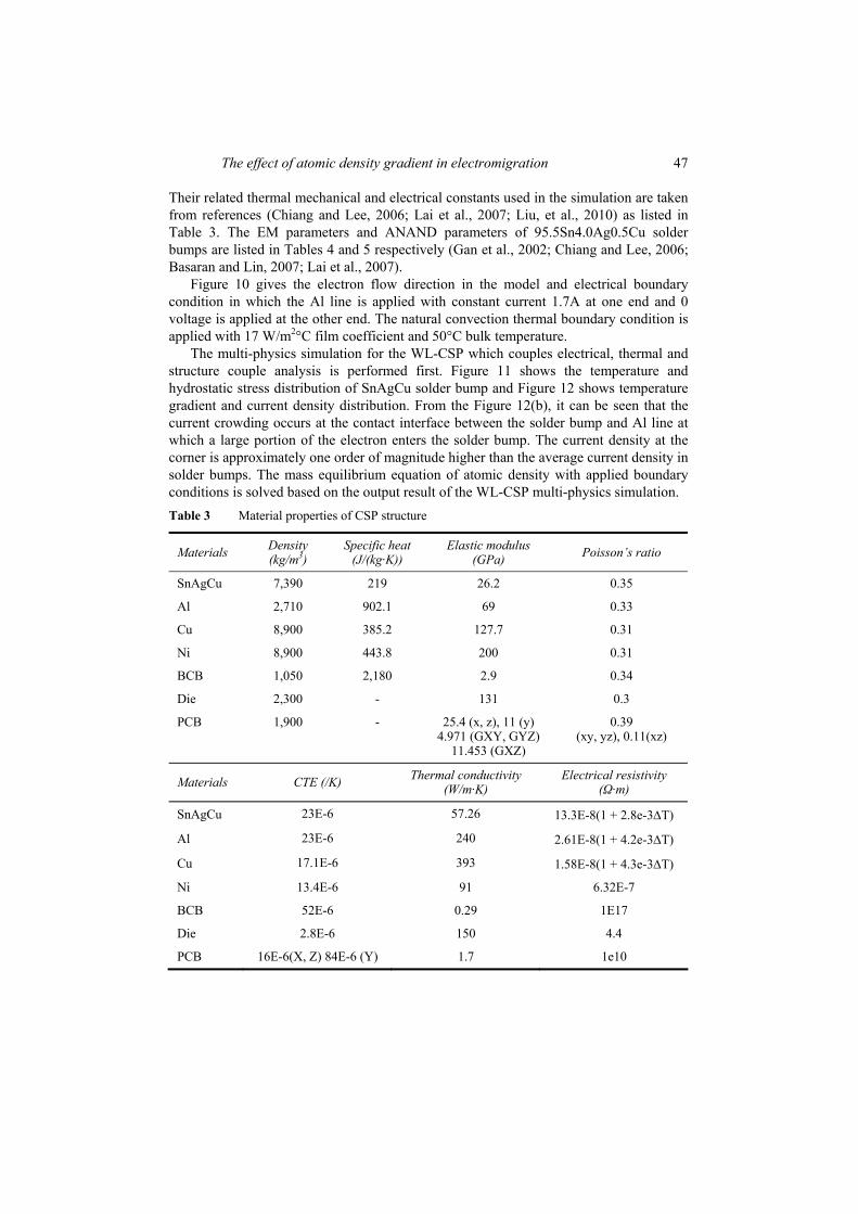
Their related thermal mechanical and electrical constants used in the simulation are taken from references (Chiang and Lee, 2006; Lai et al., 2007; Liu, et al., 2010) as listed in Table 3. The EM parameters and ANAND parameters of 95.5Sn4.0Ag0.5Cu solder bumps are listed in Tables 4 and 5 respectively (Gan et al., 2002; Chiang and Lee, 2006; Basaran and Lin, 2007; Lai et al., 2007).
Figure 10 gives the electron flow direction in the model and electrical boundary condition in which the Al line is applied with constant current 1.7A at one end and 0 voltage is applied at the other end. The natural convection thermal boundary condition is applied with 17 W/m2°C film coefficient and 50°C bulk temperature.
The multi-physics simulation for the WL-CSP which couples electrical, thermal and structure couple analysis is performed first. Figure 11 shows the temperature and hydrostatic stress distribution of SnAgCu solder bump and Figure 12 shows temperature gradient and current density distribution. From the Figure 12(b), it can be seen that the current crowding occurs at the contact interface between the solder bump and Al line at which a large portion of the electron enters the solder bump. The current density at the corner is approximately one order of magnitude higher than the average current density in solder bumps. The mass equilibrium equation of atomic density with applied boundary conditions is solved based on the output result of the WL-CSP multi-physics simulation. Table 3 Material properties of CSP structure
Materials Density (kg/m3)
Specific heat (J/(kg·K))
Elastic modulus (GPa) Poisson’s ratio
SnAgCu 7,390 219 26.2 0.35
Al 2,710 902.1 69 0.33
Cu 8,900 385.2 127.7 0.31
Ni 8,900 443.8 200 0.31
BCB 1,050 2,180 2.9 0.34
Die 2,300 - 131 0.3
PCB 1,900 - 25.4 (x, z), 11 (y) 4.971 (GXY, GYZ)
11.453 (GXZ)
0.39 (xy, yz), 0.11(xz)
Materials CTE (/K) Thermal conductivity (W/m·K)
Electrical resistivity (Ω·m)
SnAgCu 23E-6 57.26 13.3E-8(1 + 2.8e-3ΔT)
Al 23E-6 240 2.61E-8(1 + 4.2e-3ΔT)
Cu 17.1E-6 393 1.58E-8(1 + 4.3e-3ΔT)
Ni 13.4E-6 91 6.32E-7
BCB 52E-6 0.29 1E17
Die 2.8E-6 150 4.4
PCB 16E-6(X, Z) 84E-6 (Y) 1.7 1e10

48 Y. Zhang et al.
Table 4 EM parameters of 95.5Sn4.0Ag0.5Cu
Parameters Symbol Unit Value Activation energy Ea eV 1 Effective charge number Z* - –23 Self-diffusion-coefficient D0 m2/s 4.10E-05 Heat of transport Q* eV 0.0094 Atomic volume Ω m3 2.71E-29 Electrical resistivity ρ Ω·m 1.33E-07
Table 5 ANAND model parameters of 95.5Sn4.0Ag0.5Cu
Parameters Symbol Unit Value Pre-exponential factor A 1/s 500 Activation energy Q/R K 9,000 Stress multiplier ξ - 7.1
Strain rate sensitivity of stress m - .0.3 Coefficient for deformation resistance saturation value s MPa 39.4 Strain rate sensitivity of saturation value n - 0.03 Hardening coefficient h0 MPa 5,900 Strain rate sensitivity of hardening coefficient a - 1.4 Initial value of s s0 MPa 1.3
Figure 10 Electron flow direction in a global model (see online version for colours)
Electron flow
Al trace
Cu trace
Figure 11 Temperature distribution of SnAgCu solder bump (see online version for colours)
Max: 420.1 KMin: 418.2 K

The effect of atomic density gradient in electromigration 49
Figure 12 Temperature gradient and current density distribution of SnAgCu solder bump, (a) temperature gradient (b) current density distribution (see online version for colours)
Max: 162.88 K/cm Min: 48.45 K/cm
e-
Max: 2.34E+8 A/m2 Min: 1.32E+7 A/m2
e-
(a) (b)
Figures 13 and 14 compare the divergences of atomic flux with and without considering the ADG at time = 5E5 s. In Figure 13, the comparison of the AFD with and without considering the ADG is obtained for:
1 electron wind migration only
2 electron wind and the thermal migration.
Without considering ADG, it shows the negative AFD (blue colour) at the upper left edge of the solder ball in (b) and (d) cases, which means the hillock nucleation will appear at the upper left edge of solder bump. This is quite different from the previous experimental test results by Gee et al. (2005), as shown in Figure 15. The void happened at this location due to the electron flowing from this location to the bottom of the solder. Thus, the prediction by the conventional AFD method is incorrect in the solder model. Dandu et al. (2010) noticed this problem using traditional AFD method. However, with the consideration of the ADG, the AFDs in (a) and (c) cases are positive at the upper left edge of the solder ball. This implies that the void generation may happen at this location, which basically agrees with the test results. Figure 14 shows the total AFD comparison with and without considering the ADG. The results with considering the ADG give the positive AFD at the upper left edge of the ball that matches the EM test results.
Figure 13 The AFD distribution of WL-CSP structure with and without considering ADG at time = 5E5 s (unit: 1/s), (a) div( )AJ ′ (b) div( )AJ ′′ (c) div( ) div( )A ThJ J′ ′+
(d) div( ) div( )A ThJ J′′ ′′+ (see online version for colours)
Max: 2.32E-7 Min: –2.61E-10 e‐
Max: –2.82E-6 Min: –1.07E-4 e‐
(a) (b)

50 Y. Zhang et al.
Figure 13 The AFD distribution of WL-CSP structure with and without considering ADG at time = 5E5 s (unit: 1/s), (a) div( )AJ ′ (b) div( )AJ ′′ (c) div( ) div( )A ThJ J′ ′+
(d) div( ) div( )A ThJ J′′ ′′+ (continued) (see online version for colours)
Max: 2.32E-7 Min: –2.61E-10 e‐
Max: –2.82E-6 Min: –1.07E-4 e‐
(c) (d)
Figure 14 The total AFD comparison distribution of WL-CSP structure with considering ADG at time = 5E5 s (unit: 1/s), (a) with ADG div( )TotalJ ′ (b) without ADG div( )TotalJ ′′ (see online version for colours)
Max: 1.85E-8 Min: –1.54E-10 e‐
Max: –2.82E-6Min: –1.07E-4
e-
(a) (b)
Figure 15 Scanning electron microscopy (SEM) of the solder bump cracking (see online version for colours)

The effect of atomic density gradient in electromigration 51
Figure 16 The divergences of atomic fluxes with and without considering ADG at the selected nodes 325, (a) cross section of the solder ball (b) the AFD curves with considering the ADG (c) the AFD curves without considering the ADG (see online version for colours)
325
(a)
-1.0E-09
4.9E-08
9.9E-08
1.5E-07
2.0E-07
2.5E-07
0.0E+00 1.0E+05 2.0E+05 3.0E+05 4.0E+05 5.0E+05
t(s)
Div
erge
nce
(1/s)
div(J_A)'@325
div(J_A+J_T h)'@325
div(J_Total)'@325
(b)
-2.0E-04
-1.5E-04
-1.0E-04
-5.0E-050.0E+00 1.0E+05 2.0E+05 3.0E+05 4.0E+05 5.0E+05
t(s)
Div
erge
nce
(1/s
)
div(J_A)''@325
div(J_A+J_T h)''@325
div(J_T otal)''@325
(c)

52 Y. Zhang et al.
Figure 16 shows the comparison of AFD with and without considering ADG at a selected node 325 which is located at the upper left corner of the cross section of the solder ball in Figure 16(a). Figure 16(b) lists the four AFD curves with considering ADG for three cases:
1 the electron wind migration only
2 the electron wind and thermal migration
3 the total divergence of equation (2d).
It can be seen that the all the AFD curves with considering ADG at node 325 are positive. The AFD induced by thermal migration is very small. The contribution of CJ D c= − ∇ for AFD [see equation (2c)] is significant. It can be seen from Figure 16(b) that, without considering ,CJ D c= − ∇ the divergence values increase rapidly with time. When
CJ D c= − ∇ is considered, the divergence values become stable after the 1e5 seconds. Figure 16(c) lists the three AFD curves without considering the ADG for the same three cases. The results show that all of the AFD curves without considering ADG at node 325 are negative. Again, the AFD induced by thermal migration is very small.
4 Conclusions
The effect of the ADG on the AFD in EM is investigated through the SWEAT and WL-CSP structures. It is found that the ADG has impact on the AFD values in the SWEAT structure but no clear impact on the divergence trends while it does have significant impact on the solder bump structure of WL-CSP. That is why we have seen in the past that the traditional AFD method, which neglects the effect of ADG, can still obtain reasonable trend agreement with EM test in the wafer level interconnect structure. However, neglecting the ADG will result in quite different AFD solutions in such a way that will induce the failure mechanism opposite to the EM test results. Such observations have been confirmed in solder bump systems of a WL-CSP.
This paper does not include the stress migration. The impact of the stress migration with and without consideration of the ADG is more challenge which will be further discussed in another paper.
Acknowledgements
The support from Fairchild-ZJUT Microelectronic Packaging Joint Lab and Zhejiang Science Foundation (No .Y6110641) is greatly appreciated.

The effect of atomic density gradient in electromigration 53
References
Basaran, C. and Lin, M. (2007) ‘Electromigration induced strain field simulations for nanoelectronics lead-free solder joints’, International Journal of Solids and Structures, Vol. 44, Nos. 14/15, pp.4909–4924.
Chiang, K.N. and Lee, C.C. (2006) ‘Current crowding induced electromigration in SnAg3.0Cu0.5 microbumps’, Applied Physics Letter, Vol. 88, No. 7, p.072102.
Dalleau, D. (2003) ‘3-D time-depending simulation of void formation in metallization structures’, PhD thesis, University Hannover, Hannover, Germany.
Dalleau, D. and Weide-Zaage, K. (2001) ‘Three-dimensional voids simulation in chip-level metallization structures: a contribution to reliability evaluation’, Microelectronics Reliability, Vol. 41, Nos. 9/10, pp.1625–1630.
Dandu, P., Fan, X.J. and Liu, Y. (2010) ‘Some remarks on finite element modeling of electromigration in solder joints’, Proceedings of 60th Electronic Components and Technology Conference, pp.396–402, Las Vegas, NV, USA.
Gan, H., Choi, W.J., Xu, G. and Tu, K.N. (2002) ‘Electromigration in solder joints and solder lines’, Journal of the Minerals, Metals and Materials Society, Vol. 54, No. 6, pp.34–37.
Gee, S., Kelkar, N., Huang, J. and Tu, K.N. (2005) ‘Lead-free and PbSn bump electromigration testing’, Proceedings of IPACK2005, 17–22 July, San Francisco, USA.
Jeon, I. and Park, Y.B. (2004) ‘Analysis of the reservoir effect on electromigration reliability’, Microelectronics Reliability, Vol. 44, No. 6, pp.917–928.
Lai, Y.S., Chen, K.M., Kao, C.L., Lee, C.W. and Chiu, Y.T. (2007) ‘Electromigration of Sn-37Pb and Sn-3Ag-1.5Cu/Sn-3Ag-0.5Cu composite flip-chip solder bumps with Ti/Ni(V)/Cu under bump metallurgy’, Microelectronics Reliability, Vol. 47, No. 8, pp.1273–1279.
Li, S. and Basaran, C. (2009) ‘A computational damage mechanics model for thermomigration’, Mechanics of Materials, Vol. 41, No. 3, pp.271–278.
Li, S., Abdulhamid, M.F. and Basaran, C. (2008) ‘Simulating damage mechanics of electromigration and thermomigration’, Simulation, Vol. 84, Nos. 8/9, pp.391–401.
Liu, Y., Zhang, Y.X. and Liang, L. (2010) ‘Prediction of electromigration induced voids and time to failure for solder joint of a wafer level chip scale package’, IEEE Trans on Components and Packaging Technologies, Vol. 33, No. 3, pp.544–552.
Sasagawa, K., Hasegawa, M., Saka, M. and Abe, H. (2002) ‘Prediction of electromigration failure in passivated polycrystalline line’, Journal of Applied Physics, Vol. 91, No. 11, pp.9005–9014.
Sukharev, V. and Zschech, E. (2004) ‘A model for electromigration-induced degradation mechanisms in dual-inlaid copper interconnects: effect of interface bonding strength’, Journal of Applied Physics, Vol. 96, No. 11, pp.6337–6343.
Tan, C.M. and Roy, A. (2006) ‘Investigation of the effect of temperature and stress gradients on accelerated EM test for Cu narrow interconnects’, Thin Solid Films, Vol. 504, Nos. 1/2, pp.288–293.
Tan, C.M., Hou, Y.J. and Li, W. (2007) ‘Revisit to the finite element modeling of electromigration for narrow interconnects’, Journal of Applied Physics, Vol. 102, No. 3, pp.1–7.