The ATLAS Pixel Detectorgilg/PixelOverviewPaper/PixelPaper-All/pixels...The ATLAS Pixel Detector ......
85
Draft version 0.8.2 ATLAS NOTE ATL-INDET-PUB-2007-XXX December 20, 2007 The ATLAS Pixel Detector The Pixel Collaboration Abstract
Transcript of The ATLAS Pixel Detectorgilg/PixelOverviewPaper/PixelPaper-All/pixels...The ATLAS Pixel Detector ......

Draft version 0.8.2
ATLAS NOTEATL-INDET-PUB-2007-XXX
December 20, 2007
The ATLAS Pixel Detector
The Pixel Collaboration
Abstract

December 20, 2007 – 12 : 22 DRAFT 2
1 Introduction
This paper describes the pixel detector system for the ATLAS experiment at the Large Hadron Col-lider (LHC). The ATLAS detector is a general purpose detector for the study of primarily proton-protoncollisions at the LHC [?]. The pixel detector system is a critical component of the inner tracking de-tector of ATLAS [?]. The ATLAS Inner Detector (ID) provides highly ef£cient charged-particle trackreconstruction over the pseudorapidity range |η | < 2.5 [87]. The pixel detector, with approximately 80million channels, is essential to provide pattern recognition capability to meet the track reconstructionrequirements of ATLAS at the full luminosity of the LHC of L = 1034 cm−2s−1. The pixel detectorsystem is the innermost element of the Inner Detector. It is therefore the most important contributor tothe precision needed for ef£cient identi£cation and reconstruction of secondary vertices from the decayof, for example, particles containing a b-quark and for b-tagging of jets. In addition, it provides theexcellent spatial resolution necessary for reconstructing primary vertices in the proton-proton interactionregion within ATLAS even in the presence of the many multiple interactions present at the LHC designluminosity of 1034 cm−2s−1.
In the sections below, we £rst present the performance requirements for the pixel detector. This isfollowed by an overview of the system and its relationship to the Inner Detector. We then describe indetail the principal components of the pixel detector system–electronics, sensors, modules, mechanicalsystems and services. Finally, we summarize results from test beam studies of the pixel components andthe operation of about 10% of the pixel system using cosmic ray tracks.
2 Performance Requirements and Design Choices
The performance requirements of the ATLAS Inner Detector (ID) were formulated in the Inner DetectorTechnical Design Report (TDR) [?]. The pixel system is an important part of the ID and plays a majorrole in ful£lling these requirements.
The general performance requirements for the pixel system are:
• coverage of the pseudorapidity range |η |< 2.5;
• excellent transverse impact parameter resolution;
• good resolution on the longitudinal z-coordinate, allowing primary vertex reconstruc-tion with charged tracks with σ(z) < 1 mm;
• good 3D-vertexing capabilities;
• very good jet b-tagging capabilities both in the high level trigger and in the of¤inereconstruction;
• minimal material in all elements of the system in order to reduce multiple scatteringand secondary interactions;
• excellent ef£ciency of all pixel layers; and
• radiation hardness of the pixel detectors to operate after a total dose of 500 kGy or1015neq/cm2.
These performance requirements lead to the following major design choices:
• three pixel hits over the full rapidity range. The requirement to have three pixel layershas been con£rmed by a detailed study comparing a layout with two pixel hits versusa layout with three pixel hits [?];

December 20, 2007 – 12 : 22 DRAFT 3
• minimal radius of the innermost layer (b-layer), set at 5 cm due to the practical limita-tions of clearances around the interaction region beam pipe vacuum system;
• the smallest pixel size, which was £nally set to 50 µm× 400 µm by electronics designlimitations;
• the expected dose rate for the innermost layer is expected to reach 500 kGy after aboutthe £rst £ve years of LHC operation. The other layers are expected to reach the 500kGy dose after 10 or more years of LHC operation (with maximum luminosity of 1034
cm−2s−1).
3 System Overview
In this section we present a brief overview of the pixel system and its relationship to the Inner Detector.The basic parameters of the pixel system are also summarized in this section.
The pixel detector is the innermost element of the Inner Detector as shown in Figure 1. The pixeltracker is designed to provide at least three points on a charged track emanating from the center of thecollision region in ATLAS. The pixel detector and the other elements of the Inner Detector cover apseudorapidity range |η |< 2.5.
Figure 1: ****Placeholder*** Need different £gure, more labels.
The principal components of the pixel tracking system are the following:
• active region of the pixel detector, which itself is composed of three barrel layers anda total of six disk layers, three at each end of the barrel region;
• internal services (power, monitoring and cooling) and their associated mechanical sup-port structures (also supporting the interaction region beam pipe) on both ends of theactive detector region;

December 20, 2007 – 12 : 22 DRAFT 4
• a Pixel Support Tube into which the active part of the pixel detector and the servicesand related support structures are inserted and located; and
• external services that are connected to the internal services at the end of the PixelSupport Tube.
The active region of the pixel detector is shown in a schematic view in Figure 2. The active part ofthe pixel system consists of three barrel layers–Layer 0 (so-called b-layer), Layer 1 and Layer 2–and twoidentical endcap regions, each with three disk layers.
Figure 2: ***Placeholder**** Need higher res, better labels, already shown?
The basic building block of the active part of the pixel detector is a module (section ??) that is com-posed of silicon sensors (section ??), front-end electronics and ¤ex hybrids with control circuits (section??). All modules are functionally identical at the sensor/integrated circuit level but differ somewhat inthe interconnection schemes for barrel modules and disk modules. The pixel size is 50 microns in theφ direction and 400 microns in z (barrel region, along the beam axis) or r (disk region) apart from afew special pixels in the overlap region between integrated circuits on a module–see sections ?? and ??.There are 46,080 pixels in each module.
The essential parameters of the barrel region of the pixel detector system are summarized in Table 1.Modules are mounted on mechanical/cooling supports, called staves, in the barrel region. Thirteen mod-ules are mounted on a stave and the stave layout is identical for all layers. The active length of eachbarrel stave is about 801 mm. More details are given in section ??.
The two endcap regions are identical. Each is composed of three disk layers and each disk layeris identical. The basic parameters of the endcap region are given in Table 2. Modules are mounted onmechanical/cooling supports, called disk sectors. There are eight identical sectors in each disk.
The total number of pixels in the system is approximately 67 million in the barrel and 13 million inthe endcaps, giving a total active area of about 1.7 m2.

December 20, 2007 – 12 : 22 DRAFT 5
Layer Mean Number Number Number ActiveNumber Radius (mm) of Staves of Modules of Pixels Area (m2)
0 50.5 22 286 13,178,880 0.281 88.5 38 494 22,763,520 0.492 122.5 52 676 31,150,080 0.67
TOTALS 112 1456 67,092,480 1.45
Table 1: Basic parameters of the barrel region of the ATLAS pixel detector system.
Disk Mean Number Number Number ActiveNumber z (mm) of Sectors of Modules of Pixels Area (m2)
0 495 8 48 2,211,840 0.04751 580 8 48 2,211,840 0.04752 650 8 48 2,211,840 0.0475
TOTAL ONE ENDCAP 24 144 6,635,520 0.14TOTAL BOTH ENDCAPS 48 288 13,271,040 0.28
Table 2: Basic parameters of the endcap region of the ATLAS pixel detector system.
The expected instantaneous ¤uence of charged hadrons in the Inner Detector volume is shown inFigure 3. One can see that the highest ¤uences are in the region of pixel detectors, requiring radiationhard sensors, radiation hard electronics and operation at low temperatures.
The contribution of the Pixel Detector to the total Inner Detector material budget as a function ofpseudorapidity is shown in Figure 4 (radiation lengths) and Figure 5 (interaction lengths). The beampipe contribution is also shown.
Z(cm)
R(c
m)
Figure 3: Fluence of the charged particles in the ID detector per cm2 per year at the LHC designluminosity of 1034 cm−2s−1. *** Placeholder ***

December 20, 2007 – 12 : 22 DRAFT 6
0
0.2
0.4
0.6
-4 -2 0 2 4
Services
Disks
2-layer
1-layer
b-layer
Beam pipe
η
Thi
ckne
ss in
rad
iatio
n le
ngth
s
Figure 4: Material budget of the pixel detector in radiation lengths. *** Placeholder ***
0
0.05
0.1
0.15
0.2
0.25
-4 -2 0 2 4
Services
Disks
2-layer
1-layer
b-layer
Beam pipe
η
Thi
ckne
ss in
abs
orbt
ion
leng
ths
Figure 5: Material budget of the pixel detector in nuclear absorption lengths. *** Placeholder ***

December 20, 2007 – 12 : 22 DRAFT 7
4 Electronics Systems
4.1 Overview
The £rst comprehensive proposal of the pixel electronic system was described in 1997-98 in the ATLASInner Detector and Pixel Detector Technical Design Reports [1, 2]. The complete system underwentseveral revisions in the years to follow. The radiation tolerance required is 50 Mrad, corresponding to 10years of operation at nominal LHC luminosity for the external layers and 3 years for the innermost layer(B-layer). The total number of instrumented channels is 80 million, each with about 1,000 transistorsand 100 µW maximum power consumption (power for on-detector circuitry only).
4.1.1 System Architecture
A block diagram that illustrates the system architecture with the principal links to the blocks is shown inFig. 6.
Figure 6: Simpli£ed block diagram of the pixel detector System Architecture. (Original £gure needed)
Charge released by ionizing particles in the cells of the sensor array are collected by 16 front-endchips (FE) per module, arranged in two rows of eight chips. The 16 FEs are read out by a Module ControlChip (MCC). Data are transmitted from FE to the MCC using Low Voltage Digital Signalling (LVDS)serial links, con£gured in a serial star topology. The serial protocol minimises the number lines to berouted, while the star topology maximizes bandwidth and reliability. Each module is then connected tothe off-detector Read-out Drivers (ROD) through opto-links. One down link is used to transmit clock,trigger, commands and con£guration data, while one or two up-links are used for event readout. The B-layer uses two up-links to increase the aggregate bandwidth needed for the higher average hit occupancyat the minimum radius. The readout (R/O) architecture is ”data-push”. This means that each componentin the chain (FE, MCC) always transmits at the maximum rate and there is no busy mechanism to stoptransmission when buffers are full. Each upstream component in the R/O chain (MCC, ROD) has alwaysto monitor the number of events received and compare with the number of triggers sent. In case thedifference of the two is bigger than a prede£ned value, triggers downstream are blocked and emptyevents are generated for the missing ones.
The power supply system uses commercial components, adapted to the requirements of the pixeldetector, for the low (electronics) and high (sensor bias) voltages. The use of deep sub-micron electronicsand long resistive cables with signi£cant voltage drop, required the use of low voltage regulator boardsnear (10 m) the pixel detector; electronics can never see a voltage above maximum rating (4 V). Tointerface the electrical to the optical sides of the opto-links, special driver chips (DORIC and VDC) havebeen implemented and also an opto-card (Back of Crate or BOC) is used for each ROD.

December 20, 2007 – 12 : 22 DRAFT 8
4.2 Front-end Chip (FE)
4.2.1 Front-end Chip History
Small scale chips to demonstrate analog and digital architecture were developed in the second half of1990s (M72b [3], Lepton [4], Marebo [5, 6] and Beer & Pastis [3, 7]). The £rst rad-soft functionalprototypes of full size chips were submitted in 1998: FE-B al LBNL, FE-A/C (Pirate) at Bonn/CPPM.FE-B was designed using 0.8 µm HP CMOS technology and had the same basic readout architecturethat is used in the £nal chips. The FE-B charge ampli£er uses a direct cascode 1) and source follower,feedback capacitance of 4 fF, DC feedback based on the Marebo design. The discriminator used a dualthreshold, low threshold for precise timing and a high threshold to validate hit.
FE-A was made on 0.8µm BiCMOS technology from AMS, whereas FE-C was a full CMOS version.The charge ampli£er used a folded cascode input stage with feedback capacitance of 3 fF and a newimproved DC feedback. The discriminator was AC coupled, with an input fully differential bipolar pairin the A version and CMOS in the C version. The column readout architecture used an always runningshift register to transport the hit address to the bottom of the chip. Hits are associated to the level 1 trigger(L1) by counting the number of clock cycles needed for the hit to reach the column bottom. FE-A/B/Cdemonstrated all the basic ATLAS pixel performance goals in the laboratory and beam. The subsequentchip was developed using the basic concept of the ampli£er/discriminator from FE-A/C and the columnreadout architecture from FE-C. The European and US front-end design efforts joined forces to combineall of the experience gained with radiation-soft chips into a common layout for the DMILL 2)-”DurciMixte sur Isolant Logico-Lineaire” technology (known as FE-D). FE-D1 was submitted in July ’99together with DORIC and VDC chips and a prototype MCC-D0. A new production run was submitted inAug ’00 with two versions of FE-D2: one with dynamic and the other with static memory cells. This runincluded the full MCC-D2 and new DORIC and VDC chips as well. Yields of both FE and MCC wereunacceptable and work with this vendor was terminated. Work on FE-H began in Dec 1999 [8]. Thechip was almost ready but was never submitted also because of massive cost increases from Honeywell.The failure of both traditional rad-hard vendors left the collaboration with the Deep Sub-micron (DSM)approach, based on commercial process 0.25 µm CMOS and rad-tolerant layout. A major design effortinitiated in Sep 2000. Three versions (FE-I1, FE-I3 and FE-I3) were submitted using the 0.25 µm DSMprocess. The £nal chip (FE-I3) was available in late 2003. Table 3 gives a summary of the front-enddesigns developed for the ATLAS pixel detector.
Chip Year Cell size Col × Row Transis- Technology References
(µm2) torsBeer & Pastis 1996 50×436 12×63 – AMS 0.8µm BiCMOS, 2M [3, 7]M72b 1997 50×536 12×64 – HP 0.8µm CMOS, 2M [3]Marebo 1997 50×397 12×63 0.1 M DMILL 0.8µm BiCMOS, 2M [5, 6]FE-B 1998 50×400 18×160 0.8 M HP 0.8µm CMOS, 2M [8–10]FE-A/C 1998 50×400 18×160 0.8 M AMS 0.8µm BiCMOS, 2M [7, 10]FE-D1 1999 50×400 18×160 0.8 M DMILL 0.8µm BiCMOS, 2M [10]FE-D2 2000 50×400 18×160 0.8 M DMILL 0.8µm BiCMOS, 2M –FE-I1 2002 50×400 18×160 2.5 M DSM 0.25µm CMOS, 6M [11]FE-I2/I2.1 2003 50×400 18×160 3.5 M DSM 0.25µm CMOS, 6M [12]FE-I3 2003 50×400 18×160 3.5 M DSM 0.25µm CMOS, 6M [13–16]
Table 3: Summary of the ATLAS pixel front-end chips
1)The cascode is a two-stage ampli£er composed of a transconductance ampli£er followed by a current buffer.2)DMILL technology was developed by CEA, France, and then produced under license by TEMIC Matra MHS

December 20, 2007 – 12 : 22 DRAFT 9
4.2.2 Design
Chip Architecture The readout chip for the ATLAS pixel detector [13, 14] shown in Fig. 7 contains2880 pixel cells of 50 × 400 µm2 size arranged in a 18× 160 matrix. Each pixel cell contains ananalogue block where the sensor charge signal is ampli£ed and compared to a programmable threshold bya comparator. The digital readout part transfers the hit pixel address, a hit leading edge (LE) timestamp,and a trailing edge (TE) timestamp to the buffers at the chip periphery. In these buffers a time overthreshold (ToT) is calculated by subtracting the TE from LE timestamp. These hit buffers monitor theage of each stored hit by inspecting the LE time stamp. When a hit becomes older than the latency ofthe L1 trigger (3.2 µs) and no trigger signal has occurred, the hit information is deleted. Hits which aremarked by trigger signals are selected for readout. Triggered hit data are transmitted serially out of thechip in the same order of trigger arrival.
Chip-levelreadoutcontroller
Hit buffer
Column-levelreadoutcontroller
Data output
Clock
L1 Power supplies
8-bit time stamp
Address & time stamps
1. readout cell 2. readout cell
Analogue part
Configuration bits
Digital part
Time
Delayed BC clock L1
?Hit address
Hit amplitudeControl
Hit buffer cell
D/A convertor
Bump-bondpad
Slow control
Chip address
Sync
stamp
Figure 7: Simpli£ed ¤oorplan of the front-end chip (FE-I3) with main functional elements.

December 20, 2007 – 12 : 22 DRAFT 10
Charge Sensitive Preampli£er The charge sensitive ampli£er uses a single-ended folded-cascodetopology, which is a common choice for low-voltage and high gain ampli£ers. The ampli£er is optimisedfor a nominal capacitive load of 400 fF and designed for negative signal expected from n+–on–n-bulkdetectors. Special attention was put in the design of the charge ampli£er to the requirement of irradi-ated sensors, where the leakage current can reach 100nA. The preampli£er has about 5 fF DC feedbackdesign, 15 ns risetime and operates at about 8 µA bias. Since the input is DC-coupled, a compensationcircuit is implemented which drains the leakage current and prevents it from in¤uencing the bias currentof the fast feedback circuit, used to discharge the feedback capacitor. The feedback system, shown inFig. 8 uses two PMOS devices, one (M2) providing leakage current compensation and the other (M1)continuous resetting of the feedback capacitor. // An important property of this feedback circuit is that
To sensor
M1
M2
cf
cl
If
M3
Figure 8: Charge preampli£er: feedback circuit.
the discharge current provided by the reset device saturates for high output signal amplitudes. The re-turn to baseline is therefore nearly linear and a pulse width proportional to the input charge is obtained.The width of the discriminator output, Time-over-Threshold (ToT), can therefore be used to measure thesignal amplitude. The duration of the ToT is measured by counting the cycles of the master chip clock.The feedback current is 4 nA for a 1 µs return to baseline with 20 ke input. The feedback circuit used inFE-I3 has an additional diode-connected transistor M3, which acts as a level shifter so that the DC levelsof input and output nodes are nearly equal. It also simpli£es the DC coupling between ampli£er and thecomparator, now described.
Comparator Signal discrimination is made by a two stage-circuit: a fully differential low gain am-pli£er, where threshold control operates by modifying the input offset, and a DC-coupled differentialcomparator. The £rst stage has a bias of about 4µA whereas the second uses a current of about 5µA.In order to make the threshold independent of the local digital supply voltage in each pixel and on theampli£er bias current I f , a local threshold generator is integrated in every pixel. Seven-bits are used ineach pixel to adjust the discriminator threshold.
Pixel Cell Control Logic A complete block diagram of the analogue part with several additional circuitblocks is shown in Fig. 9. Each pixel has several parameters that can be tuned through a 14-bit controlregister. Those bits are:
• FDAC 0-2: 3-bits to trim the feedback I f current for tuning the ToT response.
December 20, 2007 – 12 : 22 DRAFT 11
S
Select
EnHitBus
TDAC0-6
FDAC0-2
Shutdown
Mask
Load0
Load13
TDAC0-6
GDAC0-4
FDAC0-2
EnHitBus
Mask
EnHitBus
HitBus
Shutdown
To A/D C
Select
Strobe
VCal
R low ?
Hit
8-bit D/A CIbiasIbias
Serial in Serial out
SEU tolerant RAM
Decoupling capacotor Active biasing
Global threshold D/A C
Bump-bond pad
Charge injection
M2b
Feedback D/A C
Inside readout channel
Outside readout channel
Thresholdtune
Local gnda
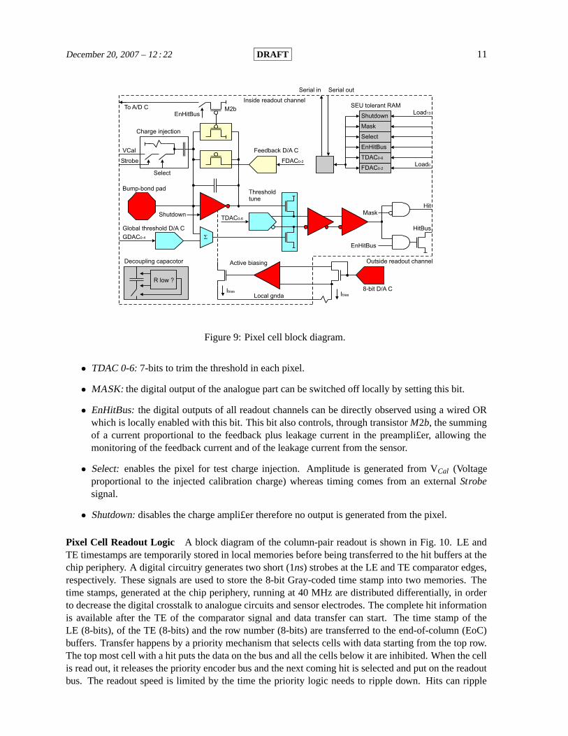
Figure 9: Pixel cell block diagram.
• TDAC 0-6: 7-bits to trim the threshold in each pixel.
• MASK: the digital output of the analogue part can be switched off locally by setting this bit.
• EnHitBus: the digital outputs of all readout channels can be directly observed using a wired ORwhich is locally enabled with this bit. This bit also controls, through transistor M2b, the summingof a current proportional to the feedback plus leakage current in the preampli£er, allowing themonitoring of the feedback current and of the leakage current from the sensor.
• Select: enables the pixel for test charge injection. Amplitude is generated from VCal (Voltageproportional to the injected calibration charge) whereas timing comes from an external Strobesignal.
• Shutdown: disables the charge ampli£er therefore no output is generated from the pixel.
Pixel Cell Readout Logic A block diagram of the column-pair readout is shown in Fig. 10. LE andTE timestamps are temporarily stored in local memories before being transferred to the hit buffers at thechip periphery. A digital circuitry generates two short (1ns) strobes at the LE and TE comparator edges,respectively. These signals are used to store the 8-bit Gray-coded time stamp into two memories. Thetime stamps, generated at the chip periphery, running at 40 MHz are distributed differentially, in orderto decrease the digital crosstalk to analogue circuits and sensor electrodes. The complete hit informationis available after the TE of the comparator signal and data transfer can start. The time stamp of theLE (8-bits), of the TE (8-bits) and the row number (8-bits) are transferred to the end-of-column (EoC)buffers. Transfer happens by a priority mechanism that selects cells with data starting from the top row.The top most cell with a hit puts the data on the bus and all the cells below it are inhibited. When the cellis read out, it releases the priority encoder bus and the next coming hit is selected and put on the readoutbus. The readout speed is limited by the time the priority logic needs to ripple down. Hits can ripple

December 20, 2007 – 12 : 22 DRAFT 12
Hit L Hit RAddrROM
LE RAM
TE RAM
LE RAM
TE RAM
Sparsescan
Sparsescan
PriL
CEUClk 24 sense amplifiersand subtraction unit
Pixel Pair (2X160 pixels)
End of Column Buffers
PriR
Fre
ezeL
WrEOC
TA CAM(4-bit)
LE CAMTOT/ADDR Write
Control
ScanScan
logicSRAM(17-bit)(8-bit)
Triggerand readoutlogic
Fre
ezeR
LE<0:7>TSI<0:7>
TA<0:3> TAI<0:3>
TO
TO
ut<
0:7>
Col
Out
<0:
4>
NXT ROCK PriIn TSC<0:7>PriOut
LE<0:7>
TE<0:7>
TOT<0:7>
ADDR<0:7>
ADDR<0:8>
Rea
dClrL
Rea
dClrR
Hitlogic
Hitlogic
Row
Out
<0:
7>
Column Arbitration Unit
Figure 10: Block diagram of the column-pair readout.
through at programmable speed that is obtained from the 40 MHz clock division. In the actual chip, themaximum speed to transfer a single hit to the EoC is 20 MHz.
Column Readout Controller Readout is column based, and two columns are readout from the samecontroller. The £rst task of the controller is the generation of the readout sequence to transfer hit infor-mation: LE and TE timestamp, plus pixel row address into an EoC buffer. This operation begins whendata is complete, which is after discriminator TE. The transfer of hits from a column pair is synchronizedby the Controller end-of-column Unit (CEU), which operates at a speed of 5, 10, or 20 MHz. A total of64-hit buffers are available for each double-column. The second task is some digital processing of thehit data. Hit information is formatted by the CEU. Formatting includes ToT calculation: subtraction ofTE time stamp from LE timestamp. Optionally, a digital threshold may be applied to ToT, a timewalk(time slewing for small charges with respect to high charge) correction may be applied (write hit twice ifbelow correction threshold, once with LE and once with LE−1), or both. These operation are pipelinedto minimize deadtime, but EoC writes cannot occur faster than 20 MHz Hit information is written to theEoC buffer, and waits there for a corresponding L1 trigger. If a trigger arrives at the correct time, checkedusing LE timestamp of hit, the data is ¤agged as belonging to a particular 4-bit trigger number. Other-wise, it is reset and the buffer is freed. Once the chip has received L1 triggers, the trigger FIFO will nolonger be empty. This initiates a readout sequence in which the EoC buffers are scanned for the presenceof hits belonging to a particular trigger number. If hits are found, they are sent to the output serializerblock, which encodes and transmits them to the Module Controller Chip (MCC). After all hits for a giventrigger number have been sent, an End-of-Event (EoE) word is appended to the data stream. All of theseoperations occur concurrently and without deadtime, with all column pairs operating independently and

December 20, 2007 – 12 : 22 DRAFT 13
in parallel.Event readout from the EoC buffers happens concurrently with the column readout. When the chip-
level readout controller starts processing a particular L1 event, it £rst broadcasts the corresponding L1readout address to all buffers. All cells with hits waiting for readout compare their stored L1 addresswith the request value. The readout of the selected L1 hits is controlled by a priority network; which sortthem in column and row order.
Chip Level Readout Controller The chip-level readout controller collects hit data from the EoCbuffers and sends out of the chip serially. All the hits belonging to the same L1 are grouped together intoa single event, and events are transmitted out of the chip in consecutive trigger order. When a L1 triggerarrives, the current bunch crossing time and a buffer over¤ow bit are stored in a 16 locations deep FIFOmemory. This allows the chip to keep track of 16 pending L1 signals. The write pointer of the FIFO isused as the L1 identi£cation, which is sent to the hit buffers. The readout sequence is started as soon asthe FIFO receives an L1 trigger. If the L1 priority scan in the hit buffers ¤ags cells with matching triggernumbers, the data of the £rst cell in the hierarchy is sent to a global data bus where the information iscopied to a shift register. The content of the shift register is then transmitted serially. This is repeateduntil the priority scan shows no more hits. An End-of-Event (EoE) data word, which includes error ¤ags,is then added to the event.
Chip Con£guration FE-I3 has 231 global con£guration bits plus 14 local bits for each of the 2880readout channels. The global bits are the settings for eleven 8-bit bias current DACs and for one 10-bitcalibration voltage DAC, global threshold bits, the L1 latency, ToT £lter thresholds, column enable bits,and others. The con£guration is loaded into the chip using a serial protocol running at 5 MHz. Thisprotocol uses three chip input pads: data input, clock and load. Each write operation begins with a 4-bitaddress, which permits the 16 chips in a module to receive independent con£gurations. The address ofeach chip is encoded with wire-bonds during module assembly.
4.2.3 Requirements and Measured Performance
Design requirements come from operation of the pixel detector at high radiation dose, from the timeresolution of 25 ns to separate two contiguous bunch crossings, from noise, from minimum operationthreshold and dispersion and from the overall power budget. Operation relies on 7-bit adjustment ofindividual pixel thresholds (tuning). The un-tuned (tuned) threshold dispersion is σ = 800 (70) electronsequivalent input charge (e). The noise is 160 e and the typical operating threshold is 4000 e, which resultsin hits > 5500e appearing in the correct 25 ns time bucket (described as in-time threshold) [15, 16].Neither the dispersion nor the noise depends on the choice of threshold. The tuned thresholds havebeen observed to re-disperse with moderate radiation dose in prototypes, and it is expected that periodicthreshold re-tuning will be needed operation. However, the actual dispersion rate in the real operatingenvironment will need to be measured. An selectable option internally duplicates near-threshold hits intwo adjacent time buckets in order to allow recovery of in-time threshold inef£ciency. Measurementsmade on few modules irradiated to 60 Mrad (in excess of the full LHC-life dose) show a negligible tunedthreshold dispersion and a 20% increase in the noise, in spite of the very high leakage current (60 nA fornormal pixels). For a con£gured chip the typical digital current is 45 mA at 2 V and the analogue currentis 75 mA at 1.6 V for a total power of 220 mW. Chip production was made in batches of 48 wafers. Thereare 288 chips on each 12-inch wafer. Six production batches were purchased with the 6 wafers from theengineering production run. The total number of wafers is 294. The average wafer probing yield wasabout 80%. The ATLAS pixel detector contains a total of 27904 front-end chips.

December 20, 2007 – 12 : 22 DRAFT 14
4.3 Module Control Chip (MCC)
4.3.1 MCC History
The prototype sequence leading up to the Module Controller Chip (MCC) is shown in Table 4. The
Chip Year # of Std.Cells # of Trans. Chip size (mm2) Technology
MCC-AMS Apr 1998 17 922 363 000 10.3×6.3 AMS 0.8µm CMOS, 2MMCC-D0 Aug 1999 – – 6.1×3.5 DMILL 0.8µm BiCMOS 2MMCC-D2 Aug 2000 13 446 328 000 11.9×8.4 DMILL 0.8µm BiCMOS, 2MMCC-I1 Nov 2001 33 210 650 000 6.38×3.98 DSM 0.25µm CMOS, 5MMCC-I2 Feb 2003 67 919 880 000 6.84×5.14 DSM 0.25µm CMOS, 5MMCC-I2.1 2003 67 919 880 000 6.84×5.14 DSM 0.25µm CMOS, 5M
Table 4: Summary of the ATLAS pixel MCC chips
very £rst version of the chip, submitted in 1998, was rad-soft and was made in AMS 0.8µm CMOStechnology [17]. This version of the chip had been extensively used when building rad-soft modules.This technology was chosen as it was very close to the 0.8 µm BiCMOS DMILL technology which, atthe time, was the chosen rad-hard technology for the ATLAS pixel detector.
A £rst prototype of the rad-hard chip (MCC-D0) was built in 1999. It contained only one Receiver,but all the remaining circuitry was implemented providing a good test of the DMILL technology. The £-nal version of the chip (MCC-D2) was submitted in Aug 2000. The chip worked £ne but an unacceptablelow yield, both in MCC-D2 and FE-D2, ruled out this technology.
At this point the MCC was ported to the DSM 0.25 µm CMOS technology and the MCC-I1 chip wassubmitted in Nov 2001. A new version of the chip, MCC-I2, was built in 2003 in order to provide betterSingle Event Upset (SEU) hardening to the chip. It turned out that the chip had a small bug that could becorrected modifying only one metal line. Six additional wafers, containing the correction in the layout,were produced in 2003 leading to the £nal MCC-I2.1 chip.
4.3.2 Design
This section brie¤y describes the actual implemetation of the production MCC chip, labeled MCC-I2.1.A simpli£ed block diagram of the MCC internal architecture is shown in Fig. 11. The MCC has threemain system tasks: (1) loading parameter and con£guration data in the FEs and in the MCC itself, (2)distributing of timing signals such as bunch-crossing, L1 trigger and resets, and (3) reading out of the FEchip and event building.
System con£guration The FE chips and the MCC must be con£gured after power-up or before startinga data-taking run. It is possible to write and read to all the MCC registers and FIFOs. This is used tocon£gure, to read status information or to test the functionality of the chip. For this last function weprovide a special set of commands that allows one to write simulated events into the FIFOs and two torun the Event Builder with the stored values in order to check the complete functionality of the chip.Once the MCC is embedded in the pixel detector, it will be important to test if the event building workswith known simulated events. Global FE chip registers and parameters in each of the pixel cells have tobe written and read back through the MCC.
Trigger, reset and timing The second task the MCC has to deal with is the distribution of L1 triggers,resets and calibration/timing signals for the FE chips. In Data Taking mode, each time a L1 triggercommand is received by the MCC the Trigger, Timing & Control (TTC) logic issues a Trigger to the

December 20, 2007 – 12 : 22 DRAFT 15
RECEIVER
1155
ReceiverFIFO
RECEIVER
CT
RL
00
25
Lv1Cnt
PendingLv1FIFO
TRANSMITTER
CT
RL
EventScoreboard
EoE
DT
O
CK
DT
I 1
5
DT
I 0
DA
O
LD CC
K
SY
NC
LV
1
XC
K
RREECCEEIIVVEERRCCHHAANNNNEELL
EEVVEENNTTBBUUIILLDDEERR
FFRROONNTT EENNDDPPOORRTT
MMOODDUULLEEPPOORRTT
REC/TRAN
RREEGGIISSTTEERRBBAANNKK TTTTCC
CCOOMMMMAANNDDDDEECCOODDEERR
PendingEvCnt
XC
KIN
DT
O2
BcoCnt
84
16 CK-Tree
DC
I
DA
TA
Figure 11: MCC block diagram.

December 20, 2007 – 12 : 22 DRAFT 16
FEs, as long as there are less than 16 events still to be processed. In case of an over¤ow the L1 triggeris not generated by the MCC and the corrsponding event is lost. The information is sent to the RODtogether with the number of missing events in order to keep up with event synchronization. In additionto the triggers, the TTC logic generates a hierarchy of reset signals that can be applied either to the MCCor to one or more FE’s.
The last function of the TTC logic is the ability to issue calibration strobes to the FEs. This is usedto calibrate the FE analogue cells on a pixel by pixel basis.
Event building The read-out architecture that was chosen for the pixel detector is a data-push archi-tecture with two levels of buffering: EoC buffers in the FE chips and 16 individual 128× 27-bit depthFIFOs (ReceiverFIFO) at the MCC inputs.
Event readout and building is by far the most complicated task and it requires that most of the chiparea to be implemented. Data received from the FEs, in response to a L1 trigger, are deserialized andbuffered into 16 FIFOs, one FIFO for each receiving FE line. These FIFOs are used to derandomisethe 16 data ¤ows from the FEs and are used by the event builder to extract ordered hits and to preparethem for transmission out of the pixel module. Event building is performed by two concurrent processesrunning in the MCC. The £rst (Receiver) deals with the £lling of the 16 input FIFOs with data receivedfrom the corresponding FE chip, while the second (Event Builder) extracts data from the FIFOs andbuilds up the event. Each FE sends data as soon as they are available with two constraints. Event hitsmust be ordered by event number and for each event an end-of-event (EoE) word is generated. EoE isalso sent for the case of an empty event to maintain the event synchronization.
The event transmitted to the ROD is organized by the Event Builder process on an event-by-eventbasis, instead of a hit-by-hit basis. If the FIFO becomes full while storing incoming hits, all subsequenthits are discarded and only the EoE word is written into the FIFO. In this case, a truncated event ¤agwill be stored in the ReceiverFIFO and then recorded to the MCC output data stream. The mechanisminsures that reconstructed events are not corrupted by FIFO over¤ows.
As soon as the Event Builder £nds that an event is completely received from all of the 16 FEs (EventBuilder knows from the Scoreboard about the existence of complete events) it starts building up andtransmitting the event. The £rst information written to the output data stream is the bunch crossingidenti£er (BCID) and the L1 identi£er (L1ID). At this point the Event Builder starts fetching data fromthe ReceiverFIFOs, until it £nds an EoE in the data. Once the Event is £nished a Trailer word is sent outin order to inform the ROD that the Event has ended.
I/O Protocols Several serial protocols were de£ned for communication to/from ROD/MCC and MCC/FE.All protocols that are active during data taking use only LVDS type signals, while signals used in thecon£guration time have single-ended CMOS to reduce the number of interconnection lines. Communi-cations from the ROD to the MCC use a 40 Mb/s data line (Data Command Input - DCI) validated bythe rising edge of the 40 MHz clock (CK).
The MCC to ROD link may use 40, 80 or 160 Mb/s data rate. For the case of 40 Mb/s a new bit istransmitted at every rising edge of the CK. For the 80 Mb/s, bits are sent at both CK transitions. Finallyfor 160 Mb/s, both lines and clock edges are used (this can be considered as a 2-bit wide serial link).Only event read-out uses the two higher bit rates. Read-out of con£guration data is always at the 40 Mb/srate. Data passing from the MCC to the ROD improved robustness by providing a bit-¤ip safe Headerand adding synchronization bits after known numbers of clock cycles.
Communications from MCC to FE chips use a serial CMOS data bus (Data Address Output - DAO),a CMOS control line (Load - LD) and a 5 MHz validation CMOS clock (Control Clock - CCK). Bothcon£guration and event data from the FE to the MCC are transmitted using 16 individual LVDS seriallinks (Data Input - DTI).

December 20, 2007 – 12 : 22 DRAFT 17
Special care has been placed in the implementation of the Data–Taking protocols in order to minimizethe effect of possible Single Event Upset (SEU) events. In particular, while in data taking mode thereare only two possible 5-bit commands: trigger and exit data-taking mode. All permutations of the triggercommand obtained by ¤ipping one single bit are also interpreted as a trigger command with the correcttiming.
4.3.3 Performance
The design requirements need to address the pixel detector operation at high radiation dose, the timeresolution of 25 ns separating two contiguous bunch crossings, the expected bandwidths at the highestluminosity, the L1 trigger rate of 100 kHz and the number of FE chips that are controlled by a module.
The 16 FIFO’s present in the MCC were designed in order to cope with expected data rate of theFE chips operating at full luminosity with a L1 trigger rate of 100 kHz. Special care has been putin making a Single Event Upset (SEU) robust design, due to the harsh radiation environment that thepixel detector will have to sustain (50 Mrad in three years of operation for the innermost pixel layer).This problem has been addressed using either triple redundancy majority logics or error detection andcorrection schemes. We irradiated several modules up to the full LHC-life dose, continuously readingout data during irradiation. From studies of the SEU, we can can extrapolate to stable operation at theLHC without a signi£cant loss of con£guration data due to bit-¤ip in the memory elements.
For a con£gured chip the typical digital current is 145 mA at 2.0 V, and a clock frequency of 40 MHzfor a total power of 290 mW. All MCC-I2.1 chips were produced in a single batch of 6 wafers. Thenumber of potentially good chips per wafer is 536. The measured yield was of 83%, providing a total of2666 good chips. A total of 1744 chips are used in the ATLAS pixel detector.
4.4 Optical Communication
4.4.1 Optolink Architecture
The communication between the detector modules and the off-detector electronics is made via opticallinks. This has been selected to obtain electrical de-coupling and minimise the material budget. Thearchitecture was inherited from the ATLAS SCT [18]. Modi£cations where made to adapt it to thedata-rates, modularities and radiation hardness needs of the pixel detector.
A block diagram of the optical-link system architecture is shown in Fig. 12. The two main com-
RX plugin
TX plugin
DORIC
Opto-Board
Opto-Board
Up
Down
LVDSPP0 PP1
rackROD
16 or 8
8
84
4
(8)
8
8
8
272
272
272
272
Back of Crate Card
VDC
6 or 71 or 2
2 or 4
272
2
PiN
array
VCSEL
array
Fibres Fibres
PIN
array
VCSEL
array
DRX
BPM-12
Module
MCC
Figure 12: Optical link System Architecture
ponents in the optical link system are the opto-board, on the detector side, and the Back of Crate Card

December 20, 2007 – 12 : 22 DRAFT 18
(BOC), on the opposite end. To keep the material budget low, to accommodate £ber routing require-ments, to control radiation exposure, and to permit the use of optical arrays, the opto components andthe related receiver/driver ICs were not installed into the detector modules. The components have beenput instead on opto-boards at Patch Panel 0 (PP0 - see section 7), at a distance of about one meter fromthe modules and at relatively large radius in the the Pixel Support Tube (PST).
The transmission of the signals from the detector modules to the opto boards uses LVDS electricalconnections. These serial connections link the MCC with VCSEL Driver IC (VDC) and the DigitalOptical Receiver IC (DORIC) sited on the opto-boards. DORIC and VDC designs were derived from theSCT project; but have been adapted to survive the higher radiation dose seen in the the pixel detector.These chips have been fabricated on the same silicon wafers used to produce the MCC chips.
The communication with each detector module uses individual £bres: one for down-link and oneor two for up-links. Trigger, clock, commands and con£guration travel on the down-link, while eventdata or con£guration read-back data travel on the up-link(s). On the down-link bi-phase mark (BPM)encoding is used to send a 40 Mbits/s control stream on the same channel as the 40 MHz Bunch Crossing(BC) clock. Decoding of the BPM channel within the DORIC recovers both the data stream and theclock signal. The use of individual links for every module permits the adjustment of the timing, used toassociate the hit to the bunch crossing, by changing the delay of the transmitted signal with respect to thephase of the LHC machine reference clock received in the BOC.
The readout bandwidth required to extract the hits from the detector modules depends on the LHCinstantaneous luminosity, on the L1 rate and on the distance between the module and the interactionpoint. Simulation of the readout architecture with generated physic events [17] shows that a bit rate of40 Mb/s for the Layer-2 modules, 80 Mb/s for the Layer-1 or Disk modules and 160 Mb/s for the B-layermodules are needed to keep the number of lost hits due to bandwidth saturation suf£ciently low. The datatransmitted in up-link are encoded in non-return-to-zero (NRZ) format. Electrical to optical conversionhappens in the opto-boards on the detector side and in the RX- and TX-pluggings in the BOC.
There are two ¤avours of opto-boards: Disk/L1/L2-boards (D-board) with 8 down-link and 8 up-link channels and B-layer-boards (B-board) with 8 down-links and 16 up-links. The B-boards use two 80Mb/s channels to obtain the aggregated bandwidth of 160 Mb/s needed for the B-layer modules. Becauseof the modularity of staves (13 modules) and of sectors (6 modules) D-boards use either 6 channels forthe disk-sectors or 6/7 channels for the half-staves in Layer-1 and Layer-2. B-boards, instead, are usedin the B-layer staves where two uplinks per module are needed.
In the off-detector part of the links, one BOC exists for each ROD. BOCs come with a variety ofhardware options that are implemented by equipping the card with a larger or smaller number of opticalreceiver (RX-plugin) or transmitter (TX-plugin) plug-ins. Each plug-in, in principle, can serve up to 8modules, but, in practice, only 6 or 7 are used due to the modularity of the detector. Each BOC has spacefor 4 TX-pugins and 4 RX-plugins. BOCs come with 4 TX and 4 RX where the maximum bandwidthrequirement is of 40 Mb/s, with 2 TX and 4 RX for 80 Mb/s and with 1 TX and 4 RX, for 160 Mb/s.Two full custom chips have been designed by the SCT collaboration and used in the optical plug-ins;they are the DRX (12-channels Data Receiver ASIC in the RX) and the BPM-12 (12-channels Bi-PhaseMark encoder ASIC in the TX). In the BOC there is also the optical S-Link interface used to send theROD output to the ATLAS Readout Buffer (ROB) units, which are the next level up in the event readoutchain.
4.4.2 opto-board
The opto-board is the opto/electro-interface on the detector side. It consists of a beryllium-oxide (BeO)printed circuit board measuring 2× 6.5 cm2. As discussed in Section 4.4.1 two ¤avour of opto-boards(D-boards and B-boards) exist and six or seven detector modules are connected to them. The D-boardsare equipped with one PiN diode array and one VCSEL-array (Vertical-Cavity Surface-Emitting Laser),

December 20, 2007 – 12 : 22 DRAFT 19
while the B-boards have a second VCSEL-array. Each opto-board loads two 4-channel DORIC chips,whereas two and four 4-channels VDC chips are loaded in the D-board and B-boards, respectively. Theoptopack, which holds the PiN/VCSEL arrays and the connector to plug the optical £bres, has a customdesign in order to ful£l requirements that it be low mass, non-magnetic and radiation tolerance. The totalnumber of opto-boards in the detector is 288. This is more than the minimum 272 (44 B-boards and228 D-boards) needed to read out the detector in order to have spares available to recover from problemsduring integration. In the end only one spare board was used. The remaining spares remain mounted inthe detector, but not connected.
PiN diode array Arrays of silicon PiN diodes are used to receive the data sent by the VCSELs. Epi-taxial silicon PiN diodes are used because the intrinsic layer provides a thin active layer allowing forfast operation at low PiN bias voltage. The active area of each individual PiN diode is circular with adiameter of 130 µm and the depth of the intrinsic region is 35 µm [18].
DORIC The DORIC integrated circuit has the function of amplifying the optical signal detected in thePiN diode and of reconstructing the clock and data channels from the BPM coding. Data and clock aretransmitted, using LVDS signal levels, to the MCC. Each DORIC chip contains four identical channels.The speci£cation for the current from the PiN diode is in the range of 40 µA to 1 maA. The requirementsfor the extracted clock are a duty cycle of 50± 4 % and a time jitter better than 1 ns. The DORIC hasbeen designed to have a bit error rate better than 10−11 after a radiation life dose. This condition isobtained with a PiN-diode bias current of less that 20 mA. The PiN diode current ampli£ers use a singleended scheme [19]. This design solution avoids the chip having to see at its inputs the diode bias voltage,which is higher than the rating for the integrated circuit technology. The DORIC must withstand up to10 Mrad over the 10 years of ATLAS operation. It is, therefore, implemented in the same proven (0.25 µm) CMOS technology as used for FE, MCC and VDC.
VDC The VDC converts the LVDS input signal, received from the MCC, into a suitable single-endedsignal to drive the VCSELs in a common cathode array con£guration. The VDC chips come with fourchannels and drive one half of the VCSELs array. An external current used to drive the VCSEL operatesup to 20 mA. The nominal current to operate the VCSEL is 10 mA. A standing (dim) current of ∼1 mAis provided to improve switching speed in the VCSEL. The dim current is remotely controlled by anexternal voltage. The requirement for the rise/fall time (20 to 80 %) is in the range of 0.5 to 2.0 ns, where1.0 ns is nominal. A further requirement, relevant to reducing the pick-up noise pertains to the constantpower consumption of the VDC, that is independent from VCSEL being bright (on) or dim (off). Avoltage (VIset ), remotely controlled, determines the current Iset that sets the amplitude of the VCSELcurrent (bright minus dim current).
VCSEL array Vertical-Cavity Surface-Emitting Laser (VCSEL) arrays are used to transmit the dataoptically. The main advantages of VCSELs are that they provide large optical signals at very low currentsand have fast rise and fall times. In order to maintain low the laser threshold current, VCSELs use ion-implants to selectively produce a buried current-blocking layer to funnel current through a small area ofthe active layer. The VCSELs [18] used in the pixel and SCT systems have an oxide implant to achievethe current con£nement, which is becoming the standard VCSEL technology as it produces lower currentthresholds at higher bandwidth. VCSELs are produced in arrays of 8 diodes. The typical £bre coupledpower per channel is greater than 1 mW at a drive current of 10 mA. This optical power at 10 mA issuf£cient to give a noise immunity of 6.2 dB. Using a slightly higher current is possible, if one addsanother 1.8 dB of noise immunity. The down-link, where the current is not a critical issue, can pro£t

December 20, 2007 – 12 : 22 DRAFT 20
from this improved margin corresponding to an higher immunity to SEU and to Bit Error Rate (BER).One mW of optical signal ensures a BER better than 10−9.
4.4.3 Back of Crate Card (BOC)
Each BOC is connected to one ROD through the crate back-plane. The BOC has two functions: interfacebetween ROD and opto-links and distribution of the timing to the on- and off-detector electronics. EachBOC receives a system clock signal and redistributes it to the pixel detector modules and ROD. Eachdetector module needs a precise phase adjustment of its 40 MHz clock relative to the bunch-crossingtime reference. The adjustment of this phase can be done for each module independently. This is madeby an ASIC (PHOS4) that contains four programmable delay channels, which are programmable in therange of 0 to 25 ns. The PHOS4 chip is also used to adjust the sampling clock that controls data receivedfrom the pixel modules. The opto-electrical conversion and the connection to the £bres is located in twocard plug-ins: TX-pluggings and RX-plugins, respectively, for transmission and reception of optical data.The TX-plugin has an 8-channel VCSEL array and a BPM-12 ASIC. The RX-plug–in has an 8-channelPiN diode array and a DRX ASICS.
DRX The DRX ASIC ampli£es, discriminates and converts the signal from the PiN diode into anLVDS signal. The comparator is DC coupled and the threshold can be controlled over a current range upto 255 µA by an external voltage reference generated by a DAC. The DRX chip was originally designedfor the ATLAS SCT detector and contains 12 channels. Only 8 channels per chip are used in the pixelBOC.
BPM-12 The BPM-12 ASIC does the encoding of clock and data in the Bi-Phase Mark format that isused in the £bre optic transmission. This chip was originally designed for the SCT detector and only 8of the 12 channels are used for the pixels. A critical speci£cation for this component is to have a shortdelay between input signals and encoded outputs because it is added to the overall L1 trigger delay. Themeasured delay value is 60 ns.
4.4.4 Opto-£bres
The connection between the BOC and the opto-boards is made with optical £bres. Two different kindsof £bres are used, Stepped Index Multi-Mode £bres (SIMM) and GRaded INdex multi-mode £bres(GRIN). SIMM £bres have been tested to be radiation tolerant but have lower bandwidth per unit lengththan GRIN £bres [20]. To optimise the bandwidth and radiation tolerance, splicing of 12 m long SIMMand 70 m long GRIN £bres has been used. The £bres are ribbonised into 8-way ribbons and 8 ribbonsmake an optical cable. The 12 m length of the SIMM £bre is segmented by a MT16 connector at∼ 2.5 mfrom PP0 (at PP1). A total of 84 cables have been installed.
4.4.5 Optolink Performance
The selection and quali£cation of the components to be used in the optolink system was done by extensivelaboratory tests, irradiation campaigns and system measurement in test beams. From the measurementsmade on single components or parts of the system, we predict a good behaviour for the optolinks over10 year of operation at LHC [19–23]. The measurement of the bit-error-rate in optolink ring-loopsrunning at 40 Mb/s (80 Mb/s) gives an upper limit BER < 1.45× 10⁻¹⁴ (BER < 3.62× 10⁻¹⁴). In factno single errors were found [24]. The method to adjust the timing in the BOC to time the pixel detectorwith a bunch crossing is reported in [25]. Using the current procedure, automatic tuning of the optolink

December 20, 2007 – 12 : 22 DRAFT 21
parameters (the system laser forward currents, PiN-diode photo-current thresholds, etc.) is achieved in(extrapolated to the whole detector system) under 10 min.
4.4.6 Production of Optolink Parts
During the quali£cation test of production components it was observed that several batches of VCSELshad a large output light power spread varying with temperature. Many VCSELs give a power, coupledto the £bre, below the speci£cation requirement (350 µW) at the nominal operating temperature insidethe pixel detector (−7C). To overcome the problem it was decided to add a temperature regulation ofthe optboards, giving the possibility to operate at 20C. One VCSEL and one PIN arrays failed duringdetector integration. In each case single channel of the array ceased to function. The cause of thesefailures was not determined. In both cases the affected modules were recovering by switching to a spareopto board in one case and by moving only one module to an unused (7th channel of a board serving only6 modules) in the other.
Optical £bres, fabricated and assembled by external companies, have been tested during productionby measuring light coupling and attenuation. Two out of 86× 8 8-way ribbons showed failures. Fibresare tested again after installation with a Time Domain Re¤ectometer and replaced by spares in case offailure.
4.5 Data Acquisition System
The pixel detector Data Acquisition System (DAQ) has been designed following the speci£cation of theATLAS global DAQ architecture [26].
4.5.1 Architecture overview
The off-detector readout architecture of ATLAS consists of two parts: a sub–detector speci£c part, wherethe Readout Buffers (ROD) are the main building blocks, and an ATLAS common design that is refereedas the Read Out System (ROS) [27].
The pixel ROD [28] is a 9U-VME module. The ROD handles the data transfer from the on-detectorelectronics on one side to the ROS system on the other side. Data from the detector arrive at the RODsthrough the BOCs. Data passes through the BOCs and is then received at the ROS by custom designedinterface modules. The ROS is a PC based system. These PCs temporarily store readout events into theirmemory and transfer only those accepted by the L2 trigger to the next level up in the readout chain.
ROD modules are plugged into ROD crates. There are 9 crates with up to 16 ROD modules per crate.In total, there are 44 modules or 3 crates for the B-layer, 38 modules for Layer-1 plus 28 modules forLayer-2 or 4 crates and 24 modules or 2 crates for the disks. A Trigger, Timing & Control InterfaceModule (TIM) [29–31] and a Single Board Computer (SBC) [32] complete the ROD crate. The TIM isthe interface to the Trigger System. The DAQ software running in the SBCs controls the modules in theROD crate. There is no event traf£c on the ROD VME–bus during normal data–taking; data are routeddirectly from the ROD to the ROS PCs [27] via fast optical links (S-Link). The VME–bus is, instead,heavily used during calibration of the pixel detector. RODs are controlled, via VME bus, by the SBCwhich also acts as interface to the global DAQ system.
Calibration data are treated differently from collision data. The procedure to calibrate the pixel de-tector consists of a sequence of injections of a known charge into the pixel’s front-end ampli£ers. Theresponse of each pixel is measured as a function of the injected charge and of other parameters (thresh-olds, preampli£er feedback currents, trigger delay) that can be varied during the calibration procedure.The typical result of a calibration sequence consists of a set of occupancy histograms corresponding todifferent values of the scanned parameters. In order to achieve maximum precision, it is important to

December 20, 2007 – 12 : 22 DRAFT 22
extract data from the FEs at the maximum speed supported by the detector links. This makes it dif£cultto extract calibration data using the normal data path, as the read-out chain from the ROS to the EventBuilder is designed to transfer only L2-trigger accepted events, while the detector links are designed tosupport the full L1 trigger rate. For this reason, during calibration runs, the ROD decodes the data streamsent by the front-end electronics, £lls occupancy histograms and stores them in memory. The histogramsare then extracted via the VME bus by the SBC and set to an analysis farm for further manipulation andarchiving.
Single Board Computer (SBC) The Single Board Computer is a commercial VP-3153) 6U VMEcard with a Pentium-M4), having 1.6 GHz clock and 1 GB memory. The card uses a Universe II5)
PCI-VME bridge. It has three gigabit-ethernet interfaces, of which two are used, one to connect to theATLAS control network and the second to the analysis farm, where histograms generated in the RODare collected. Up to 40 MB of internal RAM memory is used to cache the con£guration data neededin the pixel detector modules for a complete crate of RODs. The con£guration data, cached in the SBCmemory, are stored of¤ine in an Oracle database6) server. The memory is also used as a transfer bufferfor the histograms moved from RODs to analysis farm.
Trigger, Timing & Control Module (TIM) The TIM is the interface between a ROD crate and theATLAS trigger system. It receives a TTC £bre-link from a Local Trigger Processor (LTP), carrying LHCbunch crossing (BC) and orbit signals, the trigger signals like Level 1 Accept (L1A) and the trigger type,control/synchronisation signals like event counter reset (ECR) and synchronisation (SYN). These signalare distributed to the RODs via a custom backplane installed in the lower part of the VME crate. Onthe same backplane the busy signals generated by the RODs go to the TIM. The TIM makes a collectiveROD card Busy and sends a signal to the LTP. The LPT on reception of a Busy signal stops the L1A tothe detector electronics, thus allowing the front-end and ROD buffers to be emptied. Several features areimplemented in the TIM to operate on the trigger signal. Programmable delay on distributed triggers,generation of trigger bursts and generation of strobe signals having a £xed delay from a L1A. Moreover,the TIM can be used as a local trigger generator with programmable rate. This has been very useful forstudying ROD and DAQ behaviour on simulated event rates.
Read Out Driver (ROD) The structure of the ROD is outlined in Fig. 13, Three main sections of thedesign are the control path, data ¤ow path, and the Digital Signal Processing(DSP) Farm. The controlpath section consists of two Xilinx Field Programmable Gate Arrays (FPGA) and a Texas InstrumentsFixed Point Digital Processor (TI 320C6201 operating at 160MHz with 32MB SDRAM). The ProgramReset Manager (PRM) FPGA functions as a VME slave controller, allowing read and write access to allROD and BOC registers and a con£guration controller for all of the data path FPGAs. To enable the usersto easily upgrade the £rmware on the ROD, the PRM FPGA allows VME access to an on-board Flashmemory chip that stores the con£guration data for all of the data ¤ow path FPGAs. The Master DSPreceives commands and transmits replies to the VME host and coordinates the con£guration, calibrationand data-taking modes of the ROD. The ROD Controller FPGA is used in the control path as an interfacefor the Master DSP to the DSP farm, the BOC, and all of the internal ROD registers in the data ¤owFPGAs. It also controls all of the required, data ¤ow path speci£c, real-time functions on the ROD,including serial transmission of commands to the FE modules (two independent command streams canbe sent to two modules or group of modules), calibration mode trigger generation, and transmission of
3)From Concurrent Technologies Corporation, http://www.ctc.com4)From Intel Corporation, http://www.intel.com5)From Tundra Semiconductor Corporation, http://www.tundra.com6)From Oracle Corporation, http://www.oracle.com/

December 20, 2007 – 12 : 22 DRAFT 23
Control Path:
ROD Controller FPGA
Master DSP
Program Reset Manager FPGA
Operation, Commands, Triggers
96
Ba
ck o
f C
rate
Ca
rd / F
ron
t E
nd
Ele
ctr
on
ics S
Lin
kC
ard
Clo
ck
Fan
ou
t
Triggers and
Event ID Data
Tim
ing
Inte
rfa
ce
M
od
ule
BOCSetup Bus
Serial
Input
Links
Xon/Xoff
ROD Busy
DSP Farm (4)
Event Trapping,
Histograms
Data Path:
Formatter, Event Fragment Builder & Router FPGA,
Diagnostic Memory, S-Link Interface & SDSP DMA
DMA 4
...
S-Link
48
System
Clock
Serial Output
Links
VME64x Signals V
ME
Bu
s
40
DMA 1
Clocks
Host Port
Figure 13: Block diagram of the ROD.
TIM generated triggers and fast commands. In summary, these are the main actions performed by thecontrol path block:
• full control of ROD reset and FPGA con£guration;
• receives and executes command from the SBC via VME;
• receives module con£gurations via VME and stores them in Master DSP memory;
• transmits con£guration data to the modules;
• control of calibration procedures, transmitting triggers and con£guration data to FE modules;
• control of FE module data histograms;
• propagation of trigger commands from the TIM to the FE modules.
The structure of the ROD Data Flow Section is outlined in the block diagram of Fig. 14 The data ¤owsection receives serial data from the FE modules, packs the individual module fragments into a singleROD fragment and sends it to the ROS via a custom designed optical link called the S-Link. Four blockscan be identi£ed: the Input Link Interface, the Formatter, the Event Builder and the Router. Normalevent data ¤ows through the ROD via the Input Link Interface, which leaves the data unchanged. Itcan, however, trap the serial data stream in FIFOs (used in module con£guration or to trap an eventfor diagnostics). The FIFOs can also be loaded with events for analysis by the ROD for diagnostics.After the Input Link Interface, the Event data enters the Formatters. The Formatters convert the serialdata streams to parallel format, and £ll the de-randomizing buffers used to queue events for transmissionto the Event Fragment Builder (EFB) FPGA. An event is transmitted from the Formatters to the EventFragment Builder after the Controller FPGA sends a command notify that a Level 1 Accept has beensent to the modules. The ROD Event Fragment is constructed in the EFB using the ATLAS Event IDdata that was transmitted from the controller FPGA. In normal data taking, the primary source of the

December 20, 2007 – 12 : 22 DRAFT 24
ROD
CONTROLLER
FPGA
XC2S600-
6FG676
FORMATTER
FPGA
EFB FPGA
XC2S400-
6FG676
ROUTER
FPGA
XC2S400-
6FG456
DSP FARM
TI 320C6713
220MHz
256MB SDRAM
4x
Xoff
FORMATTER
FPGA
FORMATTER
FPGA
FORMATTER
FPGA
FORMATTER
FPGA
FORMATTER
FPGA
FORMATTER
FPGA
FORMATTER
FPGA
INPUT FIFO
32K Deep
S-Link
EVENT
FIFOs
16Kx48
2x
A
B
Event
Fragments
Xoff
Xoff
ROD BUSY
TTC
EVENT
ID
READOUT
TIM
MDSP SP
FE CMD (48)
XC2S600-6FG456 (8x)SiROD - DATA PATH
BO
C(4
8)
(48
)
(48)
H/T
Figure 14: Block diagram of the ROD Data Flow Section.
ATLAS Event ID data is the TIM with the ROD providing some additional information. After the headerand mode information is sent to the EFB the ROD Controller FPGA issues one token to the Formattersand event data is pushed to the EFB. The EFB checks L1ID and BCID values and records errors. It alsorecords any errors that were decoded or ¤agged by the Formatters. The event data is then stored in 16Kde-randomizing FIFOs (two each). There are two identical engines in the EFB transferring data at up to40MHz (total bandwidth 80 MHz). When an event is ready (header, data body and trailer in the FIFOs)it is transmitted to the Router. The Router has two main functions. The £rst one, that is the main physicsdata path, is to transmit 32 bit data words to the S-Link at 40 MHz. If the S-Link is receiving data fasterthan it can transfer to the ROS, the S-Link can assert Xoff to apply back pressure to the ROD data path.When back pressure is applied, read out of data from the EFB FIFO is stopped. When the EFB memoriesare almost full back pressure is applied to the Formatters. This will stop event data transmission from theformatter link FIFOs. The second function of the router is to trap data for the DSPs. This is performedwith no effect on the S-Link data during normal running. When the ROD is in calibration mode the DSPscan assert back pressure to pause the ROD data ¤ow.
Finally, the ROD is equipped with four Slave DSP processors (TMS320C671314)) with 256 MBmemory each. They are connected to the Router FPGA from which they can sample the produced RODfragments. Different tasks can run on the DSP processors to analyze captured events: monitoring task,used during normal data taking to compute average occupancy and detect noisy pixels or data transmis-sion errors. Calibration tasks accumulate histograms during the multi-dimensional scan procedure andperform an analysis in order to reduce the data volume to be transferred to the SBC. Durring data takingthe DSPs are spying the data-¤ow at the maximum possible rate without introducing dead time or ap-plying back pressure to the data ¤ow path. During calibration, on the other hand, the slave DSPs mustanalyze all the fragments, so they actually represent the most important limiting factor for the data rate.For this reason the code of the calibration task must be optimised, making use in the most ef£cient wayof the 128 KB internal DSP fast memory to £ll the occupancy histograms.

December 20, 2007 – 12 : 22 DRAFT 25
4.5.2 ROD Crate Software and Calibration Analysis Farm
The ROD Crate software is the interface between the ATLAS Run Control and the pixel detector DAQ.Its structure is outlined in Fig. 15.
ROD CrateAutomaticAnalysis
Monitoring
Diagnostics
AnalysisFramework
GUI
DB
DCS TDAQ ATLAS DB HLT Off-line
Operators DetectorExperts
DSP
Infrastructure
D
Figure 15: ROD software architecture.
For each ROD in the crate, a ROD Interface thread is created. This interface give access to the basicfunctionalities that an external applications can perform on the modules using the ROD. The implementedfunctions range from very basic commands (like ROD module reset and con£guration) to complicatedscan procedures. The ROD software interfaces are based on Remote Procedure Calls (RPC). They usea Common Object Request Broker Architecture (COBRA) layer called Interprocessor Communication(IPC) which is used in most ATLAS DAQ applications. These interfaces can be accessed either locallyin the ROD, from another process running in the SBC, or from a process running on a remote CPU. Onlyone application at the time can be allowed to access a given ROD; for this reason, each SBC runs a CrateBroker. Each process accessing a ROD must £rst ask the Crate Broker, verify if the requested resourceis free and allocate it. Only at this point is access to the ROD Interface granted. The last element of theROD Crate software is the Run Controller. This process is a local receiver of the commands issued bythe central ATLAS Run Control.
During normal data taking, the ROD Crate Run Control allocates all the ROD Interfaces and executesthe transitions (INITIALIZE, CONFIGURE, START, STOP) as indicated by the global Run Control.During calibrations, the Run Control disconnects the RODs, which are then controlled by a CalibrationConsole, controlling the calibration procedure. The interface/broker mechanism gives the possibility torun a calibration or a debugging session on a ROD while the others are taking data. Occasionally theamount of data produced during a calibration may be too large to £t to the SBC memory. The histogramsare then immediately moved (again using IPC) from the SBC to a remote analysis farm, which takes careof the £nal data analysis, of the generation of a new con£guration set based on the tuning/calibrationprocedure, and of archiving the results. In this way the memory of the SBC is not saturated, and a newscanning procedure is immediately started, while the analysis farm is analyzing the previous data set.

December 20, 2007 – 12 : 22 DRAFT 26
4.6 Detector Control System (DCS), Power Supplies, and Interlock System
The operation of the pixel detector modules and of the on-detector opto-components requires a complexpower supply [33] and control system [34, 35]. The following supplies are required at module and opto-board level:
• VDDA: analog low-voltage supply for the FE chips;
• VDD: digital low-voltage supply for the FE chips and the MCC;
• VDET : high-voltage supply to bias the sensor;
• VV DC: low-voltage supply for the VDC and DORIC chips;
• VPIN : PiN diode bias voltage;
• VISET : digital voltage to to adjust the VCSEL bias;
Electrical budget request for pixel modules and opto-boards is summarised in Table 5. The adjustment
Supply Supply Supply Nominal Nominal Nominal Worst Worst WorstType Voltage Current Voltage Current Power Voltage Current Power
(V) (mA) (V) (mA) (mW) (V) (mA) (mW)ModuleVDDA 10 1500 1.6 1100 1760 2.1 1300 2725VDD 10 1200 2.0 750 1500 2.5 1000 2500VDET 600 2 1.6 600 1 600 2 1200
Module total 3860 6425D-boardVV DC 10 800 2.0 280 560 2.5 490 1225VPIN 20 20 5.0 – – 20 20 400VISET 5 20 1.0 – – 2 20 60
D-board (Disk/Layer-1/Layer-2) total 1685B-boardVV DC 10 800 2.0 420 784 2.5 770 1925VPIN 20 20 5.0 – – 20 20 400VISET 5 20 1.0 – – 2 20 60
B-board (B-Layer) total 2385
Table 5: Speci£cations for module and opto-board power supplies.
of the operation conditions of the system requires a large modularity. Robust software packages are usedto monitor and control the hardware of the large system. There is, in addition, an independent interlocksystem that takes care of safety for the equipment and human operators.
4.6.1 The Hardware of the DCS
The scheme of the powering, control and interlock system is shown in Fig. 16. The main componentsunder the pixel DCS are:
• the power supplies to operate the sensors, the front end chips and the opto boards;
• the Regulator Stations;

December 20, 2007 – 12 : 22 DRAFT 27
Vvdc Data cover
CAN open
LV PS
HV PP4
DCS PCs
LV PP4
T
TCP/IPCAN open
System
BBIM
Opto BoardDetector Module
Regulator Station
SC−OLinkHV PS
Interlock
Data door
VddHV
Environm.sensors
BBM
T
Vpin/Viset
T
Vdda
BOC
power lines data
Dis
tan
ce f
rom
inte
ract
ion
po
int
interlock signals
DCS signals
controllines
Figure 16: Overview on the hardware of the pixel detector control system.
• temperature and humidity sensors plus monitoring devices for their readout;
• multi channel current measurement units;
• the Interlock System;
• the DCS computers to control the hardware.
To comply with the ATLAS grounding scheme, all power supplies and monitoring systems must be¤oating. Radiation damage during lifetime operation of sensor and on-detector electronics requires thatall power supplies have adjustable voltage outputs. For operational safety, over-current protection andinterlock input signals are available in all the power supplies. The pixel power supply system has £vemain components: low voltage power supply (LV-PS), high voltage power supply (HV-PS), RegulatorStation, Supply and Control for the Opto Link (SC-OLink), and the opto-board heater power supplies.Two low voltages supply the analog (Vdda) and digital part (Vdd) of the front-end read out electronics.Both are delivered by the LV-PS, which is a commercial component – the PL512M from WIENER 7). Toprotect the sensitive front end electronics against transients, remotely-programmable Regulator Stationsare installed as close as possible to the detector. These Regulator Stations allow an individual tuning ofthe power lines through digital trimmers.
The pixel sensors are depleted by the high voltage Vdet (up to 700 V) by the HV-PS. The HV-PS isassembled with EHQ-F607n 405-F modules provided by Iseg 8). The LV-PS and HV-PS are respectivelyconnected to the low voltage patch-panel-4 (LV-PP4) and to the high voltage patch-panel-4 (HV-PP4)that are used to distribute the power and monitor the currents of the individual lines.
The SC-OLink, a complex channel consisting of three voltage sources and a control signal, deliversadequate levels for the operation of the on-detector part of the optical link. Monitoring of temperaturesand of humidity is performed by the Building Block Monitoring (BBM) and the Building Block Interlockand Monitoring (BBIM) crates. While the £rst just provides a reading of values, the second additionally
7)WIENER, Plein & Baus GmbH, Burscheid, Germany8)iseg Spezialelektronik GmbH, Rossendorf, Germany

December 20, 2007 – 12 : 22 DRAFT 28
creates logical signals, which are fed into the Interlock System. All components of the LV-PS, HV-PS,SC-OLink in addition to the BOC boards are connected to the hardware based Interlock System, thatacts as a completely independent system. It consists of several units that guarantee safety for humanoperators as well as for detector parts. The Interlock System has high modularity; more than a thousandindividual interlock signals are distributed. This high modularity has been chosen to keep low the numberof detector modules out-of-service in case of some component failure. The Regulator System and partsof the Interlock System, installed inside the ATLAS detector, had to pass requirements of radiationtolerance; this required extensive quali£cation of many components.
Besides the LV-PS and HV-PS all other components in the system are custom designs, adapted to thepixel speci£c needs and using the Embedded Local Monitoring Board (ELMB) [36] for the monitoringthrough the DCS. ELMB is the ATLAS standard front end I/O unit for the slow control signal. The Con-trol Area Network (CAN) interface of the ELMB and its CAN-open protocol ensure a reliable and robustcommunication. Different Openness, Productivity, Collaboration (OPC) servers are used to integrate thehardware into the higher level of the software. All together 630 CAN nodes on 43 CAN busses and 48TCP/IP nodes for the LV power supplies are building the pixel control network. In total more than 44000variables need to be monitored.
4.6.2 The Software of the DCS
The DCS software has to establish the communication to the hardware, to support the operator withall required monitoring and control tools, and to provide automatic procedures for safety and for easieroperation of the detector for non DCS experts. Permanent operation and reliable data taking must beensured. Additionally, operation of the detector requires good coordination of DAQ and DCS actions,and for the of¤ine analysis relevant data must be recorded and stored into the conditions database. Thecore of the DCS software are the Prozess- Visualisierungs- und SteuerungsSoftware (PVSS), 9) projects,which run as a distributed system on eight control stations. As each part of a distributed system has itsown control and data managers (processes inside PVSS), an independent development and operation ofthe different projects is possible. The core of the control software is the Front-end Integration Tools (FIT)which establish the communication with the hardware components. For each hardware component, likethe HV-PS, the LV-PS and the different devices using the ELMBs, dedicated FIT exist. Each FIT consistsof an integration and a control part. The integration part initialises each given hardware componentand creates the data structures required to control it. The control part of the FIT instead supervisesthe operation of the same component. The hardware is mapped into the software in a device orientedway. The FITs are mainly foreseen for the DCS expert who needs to check the correct behaviour ofthe hardware. For persons that will run shift in ATLAS, a detector oriented view of the hardware isprovided by the System Integration Tool (SIT). The mapping of the read-out channels to the detectordevices is done by the SIT. The SIT creates a virtual image of the detector inside the DCS. It combinesall information which is relevant for the operation of a detector unit like a half stave, a disk or the fulldetector. Furthermore the SIT is responsible for the storing of the data into the conditions database.
The software used to operate on the detector is the Finite State Machine (FSM), this software isdeveloped in common from the four largest LHC experiments [37]. The FSM uses the geographicalorganised data structures, created by the SIT, and provides the user with a set of commands, to act onsmall or large fractions of the detector simultaneously. The actual status of the detector is returned by theFSM. Further, the proper settings and special power on sequences are performed automatically by theFSM. In addition, the FSM builds the link into the ATLAS wide control system. As part of the overallATLAS control system, the pixel FSM will receive commands from the ATLAS FSM during normal datataking. The communication between DAQ and DCS is provided by DAQ-DCS Communication (DDC),
9)PVSS is made by ETM, Eisenstadt, Austria

December 20, 2007 – 12 : 22 DRAFT 29
which provides command transfer from the DAQ system to DCS, publishes DCS values to DAQ and viceversa. For the tuning of the optical link, the DDC is critical.
The DCS hardware and software system has been fully exercised in various con£gurations duringthe prototyping and construction phase of the pixel detector, namely in the test beams, with cosmic raytests and during the integration of the pixel detector at CERN [38, 39].
5 Sensors
Sensors are the sensitive part of the pixel detector for charged particle detection and function as a solid-state ionization chamber. The sensor has to meet exacting geometrical constraints concerning its thick-ness and granularity as well as a high charge collection ef£ciency within the sensitive volume, whilesustaining a massive amount of ionizing and non-ionizing particle radiation damage. This is re¤ected onone hand in the selection of the bulk material and on the other hand with the design of the pixel structureitself.
5.1 Design
The ATLAS pixel sensor is an array of bipolar diodes on a high resistivity bulk close to intrinsic chargeconcentration made by implanting high positive (p+) and negative (n+) dose regions on each on a side ofa wafer. An asymmetric depletion region on the p+-n junction operates in reverse bias and extends overthe whole sensor bulk volume, able to collect and detect all charges produced in the volume by ionizingparticles. The sensor concept guarantees single pixel isolation, minimizes leakage current and makes thesensor testable as well as tolerant to radiation damage.
The pixel sensor consists of 250 µm thick n-bulk with n+ implants of size 400×50 µm2 on the read-out side10) and the p-n junction on the back side. Aside from increased leakage current, radiation damagewill invert the sensor bulk and then gradually increase the depletion voltage. For unirradiated sensorsthe depletion starts at the back (p) side and the pixels are not isolated from each other until full depletionof the bulk. Irradiation of the bulk leads to a change of the effective doping concentration Neff: £rst Neff
drops and then runs through type inversion with increasing Neff afterwards [40]. At the point of typeinversion, the junction moves to the front (n) side isolating the pixels and enabling operation even if thebulk cannot be fully depleted. Maximum achievable depletion is still desirable to maximize the signal.The advantage of the depletion zone for the n+-in-n design is shown in Figure 17.
Oxygen impurities in the bulk ensure high tolerance of the silicon against bulk damage caused bycharged hadrons [41, 42]. A comparison of the evolution of charge densities in standard and oxygenatedsilicon during irradiation with hadrons is shown in Figure 18a. In addition to the continuous irradiationof the sensors affecting the induced doping concentration, Neff also evolves due to thermal effects. Onshort time scales, Neff drops (bene£cial annealing), runs then through a minimum of constant damageand £nally on longer time scales increases again, (reverse annealing). See Figure 18b.
While the bene£cial annealing is not altered in oxygenated silicon, both the constant radiation dam-age (NC) is reduced and the reverse annealing (NY, see Figure 18b) is signi£cantly slowed down [41,42]producing a lower overall effective charge density in similarly irradiated samples after identical anneal-ing scenarios. Sensors built from such material exhibit deeper depletion zones at the same bias voltageand full depletion at a lower bias voltage.
10)Per sensor tile 47232 pixel implantations are arranged in 144 columns and 328 rows. In 128 columns (41984 or 88.9 %)pixels have a size of 400× 50 µm2 and in 16 columns (5248 or 11.1 %) pixels have a size of 600× 50 µm2. In each column8 pairs of pixel implantations near the center lines are ganged to a common read-out, resulting in 320 independent read-outrows or 46080 pixel read-out channels. This arrangement was chosen to allow the connection of the sensor tile to 16 electronicfront-end chips, see section ??.

December 20, 2007 – 12 : 22 DRAFT 30
(a) (b)
Figure 17: Comparison of depletion zones in n+-in-n pixel sensors before (a) and after (b) typeinversion. Before type inversion the electrical £eld grows from the backside and reaches the pixelimplants (full depletion). After type inversion the depletion zone grows from the pixel side andallows operation even if the bulk is not fully depleted.
(a) (b)
Figure 18: (a) Evolution of effective charge densities and full depletion voltage in standard andoxygenated silicon during irradiation with various hadrons. In oxygenated silicon the increaseafter type inversion induced by charged particles (pions, protons) is signi£cantly lower. (b) Evo-lution of the effective doping concentration due to annealing and reverse annealing effects. Theparameterization of this evolution is the so-called “Hamburg model” and represents an importantinput to the ATLAS pixel sensors which will operate near the point of minimal depletion voltages.In oxygenated silicon, both NC and NY are reduced [41, 42].

December 20, 2007 – 12 : 22 DRAFT 31
By choosing an appropriate temperature pro£le (i.e. operation at 0oC, short periods of +20oC duringdetector access, cooling down to some −20oC during longer operation breaks of the experiment) onetries to keep sensors near the lowest possible Neff and avoid reverse annealing to bene£t from the lowestpossible depletion voltage. Model calculations (Figure 19) of the combined effects of bulk irradiationand annealing have been performed [43]. The radiation induced increase of the intrinsic charge carrierconcentration leads to higher leakage currents and contributes to noise also. Here, cooling of the sensorsto values well below room temperature helps to reduce these effects.
Figure 19: Change of the effective doping concentration (left scale) and the voltage necessary forfull depletion (right scale) of oxygenated sensors according to irradiation and annealing effectsunder the Hamburg model for the two inner pixel detector layers in a standard (solid) and elevated(dashed) radiation scenario. (a) Layer 1 at 8.85 cm radial distance from interaction point with astandard ¤uence of 0.9× 1014 cm−2year−1 (from the 3rd year of operation), (b) the same as (a)with a 50 % elevated ¤uence, (c) b-layer at 5.05 cm radial distance from the interaction point witha standard ¤uence of 2.4×1014 cm−2year−1, (d) the same as (c) with a 50 % elevated ¤uence. Theenlarged detail (e) shows the evolution of the sensor characteristics during one year of assumeddetector operation: 100 days of beam operation with irradiation at an operation temperature of0oC, a period of about 30 days at +20oC during detector access, and cooling down to −20oCduring the rest of the year.
The positive and the negative implanted sensor wafer sides are both structured by mask processesfor implantation, metallization and deposition of silicon oxide and nitride. This double sided processingdemands precise mask steps and incorporates front-to-back mask alignment on the order of a few mi-crometers. However, this allows for a segmented n+ implantation used for de£nition of pixel cells and aguard ring structure on the p+ implanted wafer side, locating the main voltage drop on the sensor surfaceopposite to the bump connections [44,45]. The 250 µm thick high resistivity silicon bulk of 2 to 3 kΩ/cmcan be easily fully depleted before type inversion with bias voltages below 100 V. After type inversionthe depletion zone grows primarily from the segmented n+ implantation as the region of highest electric£eld into the bulk now converted to p-type.
On the sensor front side, pixel structures are arranged and isolated by moderated p-spray [45, 46]implantations which have been proven to be radiation tolerant with respect to surface damages inducedby ionising charged particles for doses up to 50 Mrad in silicon. The principal layout is shown in Figure20a. The dose of implant ions leading to the moderated p-spray isolation is regulated with a help of

December 20, 2007 – 12 : 22 DRAFT 32
a nitride layer which is opened during an additional mask step, creating a deeper high dose p-sprayregion in the center of the inter pixel gap and a shallower low dose layer everywhere else. This isolationtechnique avoids high £eld regions in the interface between pixel, isolation and bulk and ensures theradiation tolerance of the design [47, 48]
(a) (b)
Figure 20: (a) Principal layout of the moderated p-spray isolation which consist of high and lowdose areas between the n+ pixel implantations in the n bulk. Compared to other isolation pro£leslike p-stop [49] and p-spray [46] high £eld regions are avoided in the transition regions betweenpixel and bulk. (b) Layout detail of the bias grid [45] visible in the production mask for a pixeldouble row.
All 46080 read-out channels of an entire sensor tile are connected to a common bias grid structure[45] (Figure 20b) employing a punch-through connection technique to each channel which biases thewhole sensor without individual connections, but still ensures isolation between pixels. This bias gridhas been used for quality assurance measurements before any read-out electronics is connected to thesensors. An opening for each pixel in the passivation layer of the sensor allows a connection to eachchannel using a bump-bond technique (see section ??) to front-end electronics (see section ??), which isDC coupled and provides biasing for each individual pixel.
5.2 Prototyping and tests
Bulk and surface design features of the sensors have been extensively tested during the prototyping[48] and a dedicated pixel sensor quality assurance plan was developed [50]. The sensor layout hasbeen designed on four inch diameter double-sided wafers, which include three sensor tiles of about18 mm×62 mm each. During the prototyping, dedicated test structures were developed. The test struc-tures were placed on the ATLAS pixel sensor wafer surrounding the sensor tiles to allow dedicatedelectrical tests of various design features of the sensor (Figure 21).
The quality control included mechanical as well as electrical inspections and tests. Examples of vi-sual and mechanics tests are unique wafer identi£cation with the help of scratched serial numbers, visualinspection of the surface quality, a check of the mask alignments, planarity as well as thickness mea-surements of wafers. Electrical tests included measurement of the leakage current and the capacitanceof diodes with the guard ring structure. Leakage currents were monitored on sensor tiles, and on teststructures. Current and capacitance measurements were performed on oxide structures.
As an example of the bulk characteristics, the dark current on sensor tiles is monitored. The breakdown voltage is required to be well above 150 V. Figure 22 shows an example of measurements per-formed during the prototyping. While the two blue curves are examples of practically perfect diodes,

December 20, 2007 – 12 : 22 DRAFT 33
(a) (b)
Figure 21: (a) Geometrical layout of the sensor wafer. Central large structures 01, 02 and 03are the sensor tiles carrying 46080 read-out channels employed in the ATLAS pixel sensor mod-ules; structures 04 to 35 are dedicated test structures to monitor the quality of prototyping andproduction. (b) A pictorial view of the 4 inch diameter ATLAS pixel sensor wafer (p-side view).
the black curve shows a break down between 150 and 200 V and the red curve shows a very steep breakdown behaviour near the typical depletion voltage indicating a defect on the n-side of the sensor.
Since the moderated p-spray dose is one of the critical issues for the sensor design, the measurementof the p-spray dose is an important quality control test. Here, dedicated punch-through structure as wellas an oxide structure is needed to determine the oxide capacitance. An example of a punch throughmeasurement is shown in Figure 23. The idea of this measurement is to determine the current I betweenan individual pixel and the bias grid (Figure 23a) as a function of the potential difference ∆V whilethe sensor bulk is biased at −150 V. The resulting current (Figure 23b) increases for good isolations at∆V > 1 V. This together with the oxide measurement (not shown here) leads to the p-spray dose [50]. Thisexample shows the necessity for advanced quality control measurements to assure the radiation hardnessof production sensors. A few sensors had to be rejected due to these criteria during the productionprocess.
One important aspect of the present ATLAS pixel sensor is the operation under irradiation, especiallynear the end of its lifetime. Here, the main limitation of the sensor is the trapping of charge carriers inthe silicon bulk which leads to a decreasing value for the collected charge during the operation time ofthe detector. Trapping times have been determined in test beam [51], and lab set-ups [52]. Based on theoperation model (cf. Figure 19) of the ATLAS pixel sensor, the expected collected charge for minimumionizing particles passing through the 250 µm thick bulk has been predicted to be between 15 and 19 keafter irradiation ¤uxes of 8 to 12× 1014 cm−2 [53]. These are expected after 10 years of operations forsensors in layer 1 of the ATLAS pixel detector. Values agree nicely with those derived from test beamresults performed using production-like sensors [54]. Further performance features, including those ofthe sensor, were extracted under test beam conditions, which are summarized in section ??.
5.3 Production and quality assurance
Sensor tiles have been produced by two independent vendors, who went through the prototyping andquali£cation process. Based on the experience during prototyping, specialized quality assurance proce-dures were employed for the series production of sensors [55, 56] and were carried out as collaborativeeffort at four different pixel sensor institutes. Extensive cross calibration of mechanical and electrical

December 20, 2007 – 12 : 22 DRAFT 34
Figure 22: Examples of dark current vs. bias voltage curves on pre-series sensors tiles. While thetwo blue curves are examples of practically perfect diodes the black curve shows a break downbetween 150 and 200 V and the red curve shows a very steep break down behaviour near thetypical depletion voltage indicated a defect on the n-side of the sensor.
(a) (b)
Figure 23: (a) Electrical set-up to monitor the bias dot current vs. the potential difference test ona depleted substrate. (b) Example of punch through current measurements on several prototypestructures at the nominal bias voltage of 150 V. The left red curve is an example of a too lowpotential difference, which occurred during the early prototyping, compared to later productions,which ful£lled the isolation criteria of more than 1 V.

December 20, 2007 – 12 : 22 DRAFT 35
Figure 24: Information feedback for the sensor quality optimization during the various productionsteps of ATLAS pixel sensor wafers.
measurements was performed during these processes. The schematic layout of the information feedbackbetween sensor institutes and vendors during the various production steps are sketched in Figure 24.
The rate of production of ATLAS pixel sensors is shown in Figure 25. More than 2200 sensorssuccessfully passed through the quality assurance process and were available for hybridisation [57] tothe front-end electronics.
6 Modules
6.1 Overview
The sensitive area of ∼1.7 m2 of the ATLAS pixel detector is covered with 1744 identical modules,independent of their spatial position, with a small exception (see below). Each module has an activesurface of 6.08×1.64cm2. A module is assembled from the following assembly parts
• the sensor tile containing 47232 pixels covering an area of 6.34×2.44cm2
• sixteen front end electronics chips (FE) each containing 2880 pixel cells with amplifying circuitry,connected to the sensor by means of £ne-pitch bump bonding (see section 6.2)
• a 50 µm thin, £ne-pitch double-sided ¤ex-kapton foil onto which routings for signal and servicetraces are done
• a module control chip (MCC) situated on the ¤ex-kapton foil
• for the barrel modules another ¤ex-kapton foil, called a pigtail, provides the electrical connectionto the outside through a connector to which a micro cable is attached; for the disk modules themicro cables are attached without the pigtail connection (see section ?? for a description of themicrocables).
The concept of the ATLAS hybrid pixel module is illustrated in Fig. 26. Sixteen front-end chipsare connected to the sensor by means of bumping and ¤ip-chip technology. Each chip covers an area of0.74× 1.09cm2 and has been thinned before the ¤ip-chip process to ≈190 µm thickness by back-sidegrinding. A sizeable (≈25%) fraction of the front-end chip is dedicated to the End of Column (EoC)logic. Once bonded, most of the EoC logic extends out of the sensor area. Wire bonding pads at the

December 20, 2007 – 12 : 22 DRAFT 36
Figure 25: Sensor tile output in sum and per quarter for the ATLAS pixel laboratories in totalduring the production process.
output of the EoC logic are thus accessible to connect each front-end chip to the ¤ex-hybrid kapton foilby means of Al wire wedge bonding. On the ¤ex-kapton foil, copper traces route the signals to theModule Control Chip (MCC). The MCC receives and transmits digital data out of the modules. The¤ex-kapton circuitry is also used to distribute properly decoupled low voltage to all chips. These linesare dimensioned such that the voltage drop dispersion on the ¤ex be limited to ≈50 mV in order to keepall chips in the same operating range. The substrate material must have a low pin-hole probability, asit also houses high voltage (≈600 V) traces for the sensor bias. The kapton material must not degradeafter the LHC (500 kGy) irradiation doses. Passive components are added to the ¤ex-hybrid kapton fordecoupling and £ltering of the front-end chips.
The module temperature is remotely monitored via a Negative Temperature Coef£cient (NTC) resis-tor placed on the kapton circuit, and a fast interlock powers off a module when overheating occurs. Theinterlock is necessary as the large power density and the low mass of the support and cooling structureimply temperature rises of up to 10 degrees per second in case of a cooling fault.
A complete module draws 1.2 A at 1.6 V on the analog supply and 0.8 A at 2 V on the digital supply,i.e about 3.5 W per module. This value is expected to increase to about 5 W after an accumulated doseof 500 kGy.
The bump and ¤ip-chip operation results in a so-called bare module. The sixteen chips of an assem-bled module are £rst tested on a probe station to detect defects and possibly rework the module whichcan only be done at this point of the assembly chain.
Region in between Chips
The sensor pixels have dimensions of 50 µm×400 µm, except for 11% which have a size of 50 µm×600 µm,to allow for a contiguous sensitive area between chip boundaries in the long pixel direction. In the per-pendicular direction, two times four pixels under each of the two adjacent chips cannot be covered byactive pixel circuitry. These off-side sensor pixels are connected through metal lines on the sensor to 4+ 4 neighboring electronics pixels at the top of the columns in addition to the cells which lie directlyunderneath as is illustrated in Fig. 27. The resulting hit ambiguity is resolved by off-line pattern recog-

December 20, 2007 – 12 : 22 DRAFT 37
Figure 26: The barrel pixel module. (top) overview, showing the components of the module assem-bly: sensor, FE-chips, Flex-kapton-hybrid, module controcl chip (MCC), pigtail. (b) photographof a bare module, (c) photograph of a fully assembled module.
nition software. These special pixels: the 600 µm size (long pixels), the pairs connected to a singlereadout channel (ganged pixels) and the ones below the metal line connecting two ganged cells (inter-ganged pixels) have slightly degraded electrical performances due to the increased sensor capacitance(see section 6.6).

December 20, 2007 – 12 : 22 DRAFT 38
Figure 27: End region of the pixel detector at the edge of four FE-chips. The area of the sensorcovered by the chip edges is marked in grey. The pixels in between the chips (white rectangles)are connected through metal lines to another pixel underneath the chips.
6.2 Bump Bonding
Bump bonding is extensively used in the electronics industry for the attachment of integrated circuit diesto printed circuit boards or other substrates. Two different bump bonding techniques have been usedfor ATLAS: electroplated solder (PbSn) bumping [58, 60] and evaporative indium bumping [61]. Bothbump deposition processes are done at the wafer level. The principle of a bumped sensor – electronicspixel element is sketched in Figure 28. The substantial demands on the handling require that the wafersget bumped with their original thickness (∼ 700µm for the 20 cm IC wafers). Wafer thinning is doneafter bump deposition by covering the bumps with a photo resist layer and a UV releasing tape for bumpprotection and for handling. The wafers are then thinned by backside grinding to 180 µm–190 µm. Theyare diced and singulated immediately afterwards and then they are tested again on a probe station toassure that they are still functional and ready for the ¤ip-chip process.
6.2.1 The Solder Bumping and Bonding Process
In eutectic PbSn solder bumping [58, 60], the solder is deposited through electroplating. On an “underbump metallization” (UBM), which is a set of several metal layers sputtered on the contact pad forreasons of adhesion, diffusion barriers and wettability, a PbSn cylinder is galvanically grown and meltedto a sphere on the chip wafer, while the sensor wafer receives only the UBM [59, 62]. The parts aremated by ¤ip-chipping with re¤ow which provides self-alignment. The process ¤ow is displayed in [65].The distance between chip and sensor is about 20 – 25 µm, thus minimizing the cross-talk betweenelectronics and sensor. The connection resistance is smaller than 1Ω and the ultimate shear stress is≈50MPa. Pictures of a small dimension PbSn bump after re¤ow and of a sequence of bumps on anATLAS FE-chip are shown in Fig. 29.

December 20, 2007 – 12 : 22 DRAFT 39
bump−bond
sensor++
+
+
−−
−−
electronicsreadout
track
Figure 28: Blow-up sketch (not to scale) of the cross section of a hybrid pixel detector, showingone connection between a sensor and an electronics pixel cell. A a particle track releases ionizationin the sensor volume
Figure 29: left) Built-up of a eutectic PbSn solder bump [58, 60], (right) rows of a PbSn bumps(courtesy IZM-Berlin).
6.2.2 The Indium Bump Bonding Process
In the case of indium bonding, the bumps are grown by depositioning of evaporated indium on bothmating parts [63]. Bump pitches can be as low as 30 µm, but the bump height is limited to 10 µm dueto the use of a lift-off process for the removal of the polyimide evaporation mask. Bumps are depositedboth on the sensor and on the electronics. Mating is obtained by In-In thermocompression. The process¤ow is shown in [65]. Figure 30 shows a micrograph of 50 µm pitch Indium bumps deposited on twoglass samples and then ¤ip chipped together [61] at a temperature of ∼100C applying a pressure ofabout 20 N/cm2 per chip. The distance between chip and sensor after bonding is ≈10 µm.

December 20, 2007 – 12 : 22 DRAFT 40
Figure 30: Micrograph of a Indium bump deposition on Silicon at 50 µm pitch (left) and of a ¤ip-chipassembly of two 50 µm pitch bump arrays (right) on glass substrates (courtesy SELEX Sistemi Integrati,Rome) [61]
6.3 Quality Control of Bump Bonded Assemblies
Inspections before and after ¤ip-chip assembly are crucial to obtain the highest yield for functional pixelmodules. Automated inspection of bumped wafers with the combined use of a television camera and laserinterferometry allows to £nd missing bumps, merged bumps, deformed bumps or other defects as well asto measure bump height on wafers. Inspection with high resolution (2 µm) X-ray machines allows one todetect misalignment or merged/bridged bumps previously not detected or caused by the ¤ip-chip process.Both solder and indium bump bonding have been used to produce more than 2000 pixel modules by twodifferent £rms with bump defect rates of ≈10−5–10−4 at wafer level and ≈10−4–10−3 after ¤ip-chip.
6.4 Reworking of Bump Bonded Assemblies
All modules were built with Known Good Die (KGD), i.e. all die are tested prior to ¤ip-chip and onlythe good ones are used. This is a crucial requirement as the module yield goes with the nth power of theelectronics chip yield, n being the number of chips per module.
All front-end chips are also electrically tested after bump bonding, in order to check damages of thefront-end electronics or bumps for which the quality electrical contact is not adequate.
Both solder and indium bump bonded modules have been successfully reworked [62, 64] with asuccess probability of more than 95%. In both cases the operation requires heating and application of aforce pulling off the die to remove it, while leaving some metal on the bond pads. Afterwards, a new dieis ¤ipped to the sensor. The probability to properly connect all pixels in the second ¤ipping is very high.
6.5 Module assembly
Once a bare module has passed the acceptance test, it is equipped with a ¤ex hybrid to provide theconnections between the Module Controller Chip and the front-end electronics and from the ModuleController Chip to a microcable. A photograph is shown in Figure 31.
The ¤ex hybrid is a double sided ¤ex printed circuit with 50 µm substrate thickness and 25 µm Culines, manufactured by Dyconex AG (Bassersdorf, CH). It has been speci£cally designed to cope withthe maximum 600 V depletion voltage applied to the sensor. Besides the above mentioned connections,it includes also passive components for local decoupling and an NTC for monitoring of the moduletemperature.

December 20, 2007 – 12 : 22 DRAFT 41
Figure 31: Picture of an ATLAS Pixel barrel module
To facilitate testing of ¤ex hybrids, they are laminated on custom made printed circuit boards (FlexSupport Card or FSC), which were used for handling of the ¤ex themselves and after module attachment.A module is cut out from the FSC just prior to loading on the local support (see section ??).
Flex hybrids for barrel and disk modules are identical. A difference appears only when the connectorfor the link to the services is attached. For barrel modules, an additional ¤ex circuit (pigtail) is glued ontop of the ¤ex hybrid and electrically connected by wire bonding. It has a zero-insertion-force connectorwhich is £xed to the back side of the stave and used for attachement of the low-mass type-0 microcables(see section ??). Disk modules instead use higher mass copper cables that are soldered directly on the¤ex hybrid.
Because of the very different coef£cient of thermal expansion, between kapton and silicon, the glueused for attachment of the ¤ex hybrid to the bare modules needs to be distributed in a way to avoid anyexcessive mechanical coupling between the two. On the other hand, a strong binding is required in theplaces where wire bonds are needed. Therefore, glue (Dow Corning SE4445) is deposited along the padslines used for the interconnection between the ¤ex hybrids and the front-ends, below the MCC, near thehigh voltage bonding pad and, for barrel modules, below the pigtail attachment point.
6.6 Testing and selection procedure
After loading on a FSC a module can be connected to a test setup using cables with similar characteristicsto the ones that will connect the modules to the optoelectronics in ATLAS. The test setup in the laboratory

December 20, 2007 – 12 : 22 DRAFT 42
uses LVDS signals. The readout chain and control software is the same as that used for the FE and baremodule testing, except now con£gured to communicate via the MCC and uses the microcable instead ofprobe needles for connection to the integrated circuits.
The characterization procedure [66, 67] aims to certify if a module is acceptable for operation inATLAS, both from the electrical and mechanical points of view. A ranking value is determined such thatbetter modules can be selected for the most critical parts of the detector. In particular a module mustsatisfy the following conditions:
• the electronics should be tunable and have enough operation range to guarantee there will be tuningcapability to operate even after heavy radiation damage;
• the bump bonding has not been damaged by the assembly procedure and is suf£ciently strong;
• the wire bonding of MCC and FE is done correctly and is suf£ciently strong.
The testing sequence proceeds as follows:
1. a basic series of electronics tests is performed at room temperature after module assembly;
2. modules undergo a mechanical stress test, being cycled 10 times between room temperature and-30 C, with a cycle length of about 2h;
3. electronics tests at room temperature are repeated after thermal cycling and compared to the initialtests;
4. a complete module characterization is performed at -10 C, which is the expected operating tem-perature.
The last test is the most relevant for the de£nition of module quality and selection for usage in thedetector. Reduced electronics test are also performed after loading of modules into the local supports,to monitor possible damage happening after loading, which may trigger the repair or replacement of amodule.
Room temperature tests consists of
1. a basic functionality test: the module can be con£gured, the readout chain is tested by the digitalinjection and the ampli£er cells operated by the analog injection;
2. a test of module tunability: thresholds are equalized to 4000 e;
3. a threshold scan without depletion voltage applied to the sensor.
The £rst test is mainly a check of correct wire bonding or electrostatic discharge damage to the electron-ics. In the second test pixels can usually be tuned to the target threshold with a dispersion of 60 e, and anoise which ranges between 120 e for standard pixels to 300 e for long and ganged pixels (£gure 32).
The second and third tests are also sensitive to bump bonding properties. Pixels which fail the tuningusually correspond to a cluster of merged bumps. In this case several cell ampli£ers are shorted together,resulting in reduced sensitivity to the injected pulse. In the case of an undepleted sensor, instead, normalpixels are affected by the large parasitic capacitance of the sensor, but pixels not connected to the detectorstand out because the noise level remains low, independently of the bias voltage applied to the sensorside. Example of modules with such defects are shown in Figure 33.
During the detector construction, the test of modules before and after the thermal cycles has been ofparamount importance:

December 20, 2007 – 12 : 22 DRAFT 43
Threshold (e): VCAL scan internal - FLEX 1.Module "511587"
46079 out of 46080 pixels with good fit
Constant 8173Mean 4163
Sigma 56.06
Threshold (e)3500 4000 4500 5000 5500
1000
2000
3000
4000
5000
6000
7000
8000
Constant 8173Mean 4163
Sigma 56.06
Threshold distribution
Noise (e): VCAL scan internal - FLEX 1.Module "511587"
46079 out of 46080 pixels with good fit
Constant 4749
Mean 180.9
Sigma 11.3
Noise (e)150 200 250 300 350 400 450
500
Constant 4749
Mean 180.9
Sigma 11.3
Noise distributionConstant 1035
Mean 201
Sigma 13.1
Noise (e)150 200 250 300 350 400 450
200
400
600
800
Constant 1035
Mean 201
Sigma 13.1
Noise distribution long
Constant 167.6
Mean 306.5
Sigma 31.44
Noise (e)150 200 250 300 350 400 450
20
40
60
80
100
120
140
160
Constant 167.6
Mean 306.5
Sigma 31.44
Noise distribution ganged
Constant 250.4
Mean 203.4
Sigma 15.96
Noise (e)150 200 250 300 350 400 450
50
100
150
200
250Constant 250.4
Mean 203.4
Sigma 15.96
Noise distribution inter-ganged
Figure 32: Threshold (left) and four noise (right) distributions - for different locations and types/sizes ofpixels - of a typical module (normal, long, ganged, inner-ganged). The thresholds are uniform for theentire modules.
• debugging the failures observed in the functionality test, a problem in the potting technique for theMCC was found, which resulted in unreliability of the wire bonds, which has been corrected forthe whole production;
• comparison of bump damage between the initial assembly and the end of thermal cycling, allowedto disentangle damages due to bad handling during the assembly, which are done once and arestable in time, and damages due to weak bonds, for which there is a steady increase of disconnectedbumps with time.
The full characterization at the nominal operational temperature of -10 C includes additional checks oftunability and operational range:
• MCC operation was checked between 1.6 and 2.5 V, showing a typical turn-on at 1.8 V.
• FE operation was tested within wide ranges of digital and analog low voltage supply (VDDA1.5-2.0, VDDD 1.9-2.3).
• The ampli£er feedback current was tuned so that the average ToT response to a minimum ionisingparticle corresponded to 30 clock cycles: with the LVL1 trigger latency expected during operation,this setting provided 99.5% ef£ciency in a test beam [68]
• Timing measurements have been performed to check the timewalk performance of the FE elec-tronics when attached to the sensor. The overdrive needed to assign a signal to the correct beamcrossing is about 1000 e.
• A measurement with the 60 keV X-ray of an 241Am source, checked the detector’s response to asignal delivered directly to the sensor (see Figure 33).

December 20, 2007 – 12 : 22 DRAFT 44
Figure 33: Noise distribution for a Selex module without sensor bias (top). Disconnected regions arevisible as low noise spots. For comparison below is a hitmap obtained with an 241Am source.

December 20, 2007 – 12 : 22 DRAFT 45
The source measurement is especially relevant in accessing module quality, since, being self-triggering,is very sensitive to noisy channels. The duration of the measurement is chosen to reach an expectedoccupancy of at least 10 hits in every pixel channels. Therefore it is also very effective in uncoveringinef£cient cells, due to merged or disconnected bonds.
The number of dead channels at the source test is the £rst entry in a ranking function which has beenchosen in order to evaluate module quality. Besides defective channels this function includes:
• a χ2-like term, describing how the analog performance of a module differs from the average one;
• penalties for anomalous values of the leakage current or module bowing, which may give problemsduring operation;
• penalties for any repair operation performed on the modules.
This ranking function was used for module selection for further assembly. The distribution of the rankingfunction is displayed in Figure 34. The bump in the ranking distribution around 300 corresponds tothe set of modules that needed a full rebonding of the MCC, because of the potting problem mentionedabove. The B-Layer has been built using modules with penalty lower than 60, corresponding to a channelinef£ciency better than 0.13%. Modules with penalties higher than 1000 were not accepted for assembly.Analysis of the ranking showed an overall equivalence of all the different assembly laboratories, whilepointing out a clear difference between the two bump vendors.
The main reason for the difference is the higher number of disconnected bumps in the In-bumpedmodules. As stated before, a clusterized set of disconnected bumps may be the seed for a widening ofthe disconnected region. Because of that a ranking penalty of 202 was added for each FE chip containingmore than 30 disconnected bumps. In hindsight this penalty has been found to be quite conservative, butit is the main reason for the tails in Figure 34.
During the £nal phase of module production, when it was clear that there were a suf£cient numberof spare bare modules, only the ones with clusters of less than 4 disconnected bumps were selected formodule assembly, resulting in an improvement of module ranking.
6.7 Production yield
Statistics for the production yield of bare modules are summarized in Table 6. Most losses were due tosensor damage, bad bumping and FE damage.
Sensor damage usually is detected by an early breakdown voltage in the sensor tiles previouslypassing the sensor quality cuts. The lossrate was similar for both bump vendors and results in about 3%of the modules being rejected.
Bad bump bonding and FE damage were repairable according to the reworking procedures outlinedpreviously. The failure rate and the possibility of reworking differed between the two bump vendors.
In the case of bump problems, IZM often performed internal reworking after the in-house X-rayinspection, reprocessing the bumps. For indium bumps, there was no possibility to reprocess the bumpdeposition. If the damage was too widespread, the module was not submitted for reworking. This resultedin an overall higher failure rate.
FE damage was due to silicon shards trapped between the sensor and the FE chip, which, during ¤ip-chipping break the surface of the FE chips, resulting in shorts between the metal layers. The problemwas much more severe on Indium-bumps, given the smaller bump height. Replacement of the FE chipusually resolved the problem, but manually removing the shards from the detector surface was neededto reach a good reworking ef£ciency. Statistics for the production yield of modules are summarized inTable 7.

December 20, 2007 – 12 : 22 DRAFT 46
IZM
SELEX
Figure 34: Module ranking distribution.

December 20, 2007 – 12 : 22 DRAFT 47
Selex IZM Totalmodules yield modules yield modules yield
Assembled 1468 1157 2625Rejected 172 11.7% 35 3.0% 207 7.9%Accepted 1296 88.3% 1122 97.0% 2418 92.1%as delivered 1101 75.0% 1035 89.5% 2136 81.4%after reworking 195 13.3% 87 7.5% 282 10.7%
Table 6: Bare modules production yield
Selex IZM TotalModules Yield Modules Yield Modules Yield
Assembled 1190 1122 2312Accepted 1025 86.1% 1075 95.8% 2100 90.8%B-Layer quality 281 23.6% 445 39.7% 726 31.4%not B-layer quality 744 62.5% 630 56.1% 1374 59.4%Not accepted 165 13.9% 47 4.2% 212 9.2%Ranking¿1000 68 5.7% 10 0.9% 78 3.4%at least one dead FE 71 6.0% 10 0.9% 81 3.5%could not complete testing 26 2.2% 27 2.4% 53 2.3%
Table 7: Module production yield
Modules which did not complete the testing were usually due to mechanical damage observed afterthe assembly procedure, either induced by handling or because of weak parts which had passed theprevious quality control steps.
Modules containing one or more FE which could not be operated were also discarded from theproduction path. A loss of about 1% was due to defects in the path from the MCC to the FE through the¤ex hybrid. For Indium-bump modules, the additional yield loss is due to shorts on the FE, similar to thebehavior observed on bare modules. These defects are concentrated on reworked modules and modulesthat underwent multiple shipments. They can be assumed to be the same defect of crystal shards as seenon bare modules, which is not present after the initial bonding, but is £nally produced by the additionalmechanical stress in the module assembly.
Besides these two classes, all the other modules were operational, and a ranking is used to select thebest ones. The difference in ranking distribution between the Indium and solder bump modules is mainlydue to regions of disconnected bumps, discussed in section 6.6.
Overall the yield for module production exceeded the target, which was 90% for each step in the baremodule assembly, and the full module assembly and characterization.
7 Mechanical Systems
7.1 Overview
7.2 Barrel Region

December 20, 2007 – 12 : 22 DRAFT 48
7.3 Endcap Region [Version of November 23, 2007]
The active elements of the pixel detector in the two endcap regions are disk sectors, each supportingsix modules (three on each side). Eight disk sectors are supported on a disk support ring, forming adisk. There are three disks in each of the two endcaps. The disks in the endcaps are rigidly held by asupport frame constructed from carbon composites. This section will describe the construction, surveyand testing of the disk sectors (7.3.1), disks (7.3.2) and endcaps (7.3.3).
7.3.1 Disk Sectors
7.3.1.1 Construction
The local support structures (with integrated cooling) for the modules in the endcap region are calleddisk sectors. The sectors are roughly trapezoidal in shape, and consist of two thin carbon compositesheets with a rectangular aluminum cooling tube and carbon foam in between the sheets. The coolingtube is bent into a W-like shape to £t within the sector, and makes contact with the carbon compositesheets with a compliant, thermally conducting adhesive. Each cooling circuit in the disk region servestwo sectors.
[Text here from Gil on the physical construction of the sectors.]
Three modules are mounted on each side of the sector, with the long dimension of the module in theradial direction. The three modules on the back of the sector are rotated 7.5 degrees with respect to themodules on the front side, thus providing full overlapping azimuthal coverage. Figure 35 shows threemodules mounted on the front side of a sector.
Figure 35: Three endcap pixel modules mounted on the front side of a sector.
The modules are glued to the sectors with Dow Corning silicone SE4445. Nylon £laments of 110 µmdiameter are used to control the silicone thickness. During the gluing operation the position of survey

December 20, 2007 – 12 : 22 DRAFT 49
targets in the corners of each module are viewed with an optical SmartScope, to ensure that the modulesare placed in the correct positions on the disk sectors. The modules are positioned and glued on eachsector with a precision of 2 µm in the plane of the module and about 10 µm perpendicular to the moduleplane.
7.3.1.2 Sector Survey
After the modules are glued to the carbon surface of the disk sectors, the sector is again mounted onthe table of an optical SmartScope. The SmartScope very precisely measures X,Y coordinates (in theplane of the sector) by measuring the position of the table, and measures Z coordinates (perpendicular tothe sector) with optical focusing. The SmartScope is used to measure the X,Y position of survey targetsat the 4 corners of modules mounted on a disk sector, and these measurements are used to determine theposition and orientation of the module in the plane of the sector. The SmartScope also measures 32 X,Y,Zpoints on the top side of modules mounted on a sector (16 along one long edge, 16 along the other longedge) in the vicinity of the £rst and last chip ID pads of each front-end chip, and these measurements areused to determine the position and rotations of the module out of the sector plane. The pixel module istreated as a ¤at rigid plane, as the module distortions (such as bow) are very small.
From the above SmartScope measurements the alignment parameters of each module were calculatedin the local module reference frame. The module alignment parameters are those 6 parameters used todescribe a ¤at plane: X, Y, Z, Φx, Φy, Φz. X is the coordinate across the short width of the module, andY is the coordinate along the long length of the module. In the local module reference frame the modulealignment parameters are the displacements of the module from its nominal position (i.e. the differencefrom nominal). The X,Y,Φz alignment parameters calculated from the sector surveys are not the £nalsurvey alignment parameters, as they do not include the effect of the placement of the sector on the diskring. Details about the calculation of the module alignment parameters are given in [69].
In Figure 36 are the distributions of the X,Y,Φz module alignment parameters calculated from thesector surveys (treating all the modules as A Disk modules, which means plotting the negative of theactual X and Φz values for the C Disk modules), and in Table 8 are the means and sigmas of the Gaussian£ts to these distributions. One sees several features:
• The mean of the X alignment parameter distribution is different for front and back modules:−2.8 µm for front modules, and +2.8 µm for back modules. This is due to a small systematicoffset when the modules were mounted on the sectors. The opposite sign occurs when convertingthe survey measurements to the same coordinate system.
• The average sigma for the X and Y alignment parameter distributions is 2.0 µm, and the sigma forthe Φz alignment parameter distribution is 0.064 mrad. These resolutions include both the place-ment accuracy and the measurement precision, and thus represent upper limits on the placementaccuracy. These small values show that the modules have been placed on the sectors with excellentaccuracy of better than 2 µm.
7.3.1.3 Sector Testing
Electrical and thermal tests are performed on the modules after they are glued onto the sectors.The goal is to check any degradation of module performances (early breakdown, increased noise, bumpfailures, etc.) caused by thermal or mechanical stresses from loading. Another aim is to rank the sectorsfor disk loading so that the sectors with the least number of bad pixels can be loaded onto the innermostdisks. The tests performed on each module are part of the full quality control procedure of the ATLAS

December 20, 2007 – 12 : 22 DRAFT 50
X for Front Modules (microns)-20 -10 0 10 20
Nu
mb
er o
f M
od
ule
s
0
5
10
15
20
25a)a)
X for Back Modules (microns)-20 -10 0 10 20
Nu
mb
er o
f M
od
ule
s
0
10
20
30
40
50b)b)
Y for Front & Back Modules (microns)-20 -10 0 10 20
Nu
mb
er o
f M
od
ule
s
0
10
20
30
40
50 c)c)
for Front & Back Modules (mrad)ZΦ-0.4 -0.2 0 0.2 0.4
Nu
mb
er o
f M
od
ule
s
0
10
20
30
d)d)
Figure 36: X,Y,Φz alignment parameters calculated from the sector surveys.
Pixel Detector and more details are given in [70]. The electrical sector testing sequence consists of thefollowing three sets of basic monitoring scans:
• LOAD test: This test is performed immediately after sector loading at room temperature. The testincludes I-V, digital, analog threshold, crosstalk and source scans. Data from this test are comparedto the single module BURN test (a test performed under similar conditions before the module wasloaded on the sector) to observe any changes due to sector loading. All six modules on the sectorare tested individually before proceeding to the next test.
• INBURN test: During this test the sector is cold soaked for a period of about 12 hours at -30Cwith the power off. It is then thermal cycled between -20C and 20C (TNTC=-16 to 25C) withthe power on. The dwell time at each endpoint is 1 hour and the entire test consists of 14 cycleswith about 3.5 hours per cycle. Digital and analog threshold scans are run throughout the burn-in,while monitoring TNTC and digital/analog voltages and currents.
• STAVE test: The full electrical characterization is performed after burn-in at operating temperature(TNTC= -5 to -10C) for a fully con£gured module. The test includes all LOAD scans as well asMonLeak, in-time threshold and GDAC scans. Data from this test are compared to the singlemodule FLEX test to detect any changes due to sector loading or sector burn-in, and serve as thebasis for sector ranking.

December 20, 2007 – 12 : 22 DRAFT 51
Mean SigmaX for Front Modules −2.8±0.2 µm 2.1±0.2 µmX for Back Modules +2.8±0.1 µm 1.4±0.1 µmY for Front and Back Modules −0.1±0.1 µm 2.3±0.1 µmΦz for Front and Back Modules −0.011±0.004 mrad 0.064±0.004 mrad
Table 8: Results of the Gaussian £ts to the sector survey distributions in Figure 36.
Electrical testing and burn-in were performed using one setup. The details of the technical descriptionare given in [71]. The standard module testing hardware chain was used: a PC computer with VME andGPIB interfaces (control cards), ATLAS Pixel TurboDAQ software, a VME crate with a custom board(ATLAS Turbo Pixel Low Level card), an external custom board (ATLAS Turbo Pixel Control Card),GPIB controlled off-the-shelf power supplies, and a LBNL custom designed SURF board with module(s)attached to it. Two surf boards [72] were used to connect all six modules at once. The sector was cooledusing an inert ¤ourocarbon C6F14 running in a secondary loop connected to the sector cooling pipes.Dynalene (HC-50) was used in the primary loop and was cooled using a chiller. The two loops madethermal contact inside a coiled heat exchanger.
The following measurements made during the electrical tests described above were used to rank thesectors: bias current at 150 V, number of bad pixels in digital scans, number of bad pixels in analogthreshold scans, number of bad pixels in crosstalk scans, number of bad pixels in in-time scans, numberof bad pixels due to bump discontinuity, number of dead or masked pixels measured during source scans,threshold dispersion, and average noise.
The cuts for bad pixels are de£ned according to guidelines from the ATLAS Pixel Detector col-laboration. The above quantities were entered into the Pixel DataBase to maintain a comlete record ofthe production sequence and allow the possiblity of tracing any eventual problems. Sector evaluationalso considered results from the alignment survey and thermal performance measurements during theelectrical tests.
The total number of bad pixels in each of the endcaps can be estimated using the results of theSTAVE test performed at the sector level since this is the last, full electrical characterization performedon the modules at operating temperature. It is also the last source scan where bump discontinuity can beaccurately measured. Table 9 shows the total number of bad pixels for each of the endcaps, classi£ed byfailure. Bad pixels are not double counted: if a pixel is bad digitally, it is not counted as analog bad orsource bad.
EndCap SOURCE MASK DIG ANA DISC XTALK INTIME TOTAL %A 5497 373 5816 471 2559 171 2671 17531 0.26C 4221 360 52 594 636 127 3131 9036 0.14
Table 9: Number of bad pixels for each endcap, classi£ed by failure. Results are taken from the STAVEtest and later connectivity tests.
7.3.2 Endcap Disks
7.3.2.1 Construction
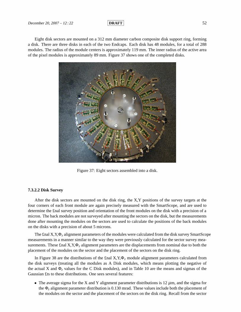
December 20, 2007 – 12 : 22 DRAFT 52
Eight disk sectors are mounted on a 312 mm diameter carbon composite disk support ring, forminga disk. There are three disks in each of the two Endcaps. Each disk has 48 modules, for a total of 288modules. The radius of the module centers is approximately 119 mm. The inner radius of the active areaof the pixel modules is approximately 89 mm. Figure 37 shows one of the completed disks.
Figure 37: Eight sectors assembled into a disk.
7.3.2.2 Disk Survey
After the disk sectors are mounted on the disk ring, the X,Y positions of the survey targets at thefour corners of each front module are again precisely measured with the SmartScope, and are used todetermine the £nal survey position and orientation of the front modules on the disk with a precision of amicron. The back modules are not surveyed after mounting the sectors on the disk, but the measurementsdone after mounting the modules on the sectors are used to calculate the positions of the back moduleson the disks with a precision of about 5 microns.
The £nal X,Y,Φz alignment parameters of the modules were calculated from the disk survey SmartScopemeasurements in a manner similar to the way they were previously calculated for the sector survey mea-surements. These £nal X,Y,Φz alignment parameters are the displacements from nominal due to both theplacement of the modules on the sector and the placement of the sectors on the disk ring.
In Figure 38 are the distributions of the £nal X,Y,Φz module alignment parameters calculated fromthe disk surveys (treating all the modules as A Disk modules, which means plotting the negative ofthe actual X and Φz values for the C Disk modules), and in Table 10 are the means and sigmas of theGaussian £ts to these distributions. One sees several features:
• The average sigma for the X and Y alignment parameter distributions is 12 µm, and the sigma forthe Φz alignment parameter distribution is 0.130 mrad. These values include both the placement ofthe modules on the sector and the placement of the sectors on the disk ring. Recall from the sector

December 20, 2007 – 12 : 22 DRAFT 53
survey results (which only include the placement of the modules on the sector), that the averagesigma for X and Y was 2.0 µm, and the sigma for Φz was 0.064 mrad. Thus we see a much largervariation in the module position due to the sectors being placed on the disk ring than due to themodules being placed on the sector.
• The mean of the Y alignment parameter distribution is 35 µm. The local module Y direction isthe radial direction in the disk. The reason that the Y alignment parameter is so large is mostlybecause the average radius of the mounting holes in the disk rings is larger than the nominal valueof 156 mm. From independent disk ring measurements, the radius appears to be roughly 25 µmlarger than nominal. This accounts for the major part of the 35 µm.
X for Front Modules (microns)-50 0 50
Nu
mb
er o
f M
od
ule
s
0
5
10
15
20 a)a)
X for Back Modules (microns)-50 0 50
Nu
mb
er o
f M
od
ule
s
0
5
10
15
20 b)b)
Y for Front & Back Modules (microns)0 50 100
Nu
mb
er o
f M
od
ule
s
0
10
20
30
40
50c)c)
for Front & Back Modules (mrad)ZΦ-0.5 0 0.5
Nu
mb
er o
f M
od
ule
s
0
10
20
30
40 d)d)
Figure 38: Final X,Y,Φz alignment parameters calculated from the disk surveys.
Mean SigmaX for Front Modules −0.1±1.1 µm 12.6±0.9 µmX for Back Modules 1.1±1.0 µm 11.5±0.8 µmY for Front and Back Modules 35.3±0.7 µm 11.4±0.6 µmΦz for Front and Back Modules −0.029±0.008 mrad 0.130±0.009 mrad
Table 10: Results of the Gaussian £ts to the disk survey distributions in Figure 38.

December 20, 2007 – 12 : 22 DRAFT 54
7.3.2.3 Disk Testing
After the sectors were mounted on a disk ring, a continuity test was performed on the modules.Its purpose was to quickly check that the delicate module circuitry survived the mounting operationand any sector or disk handling. Since it was done without cooling, at room temperature, the moduleswere powered on a chip-by-chip basis, one-at-a-time, and only for a short time. The continuity test wasperformed as each sector was mounted on the disk ring, and again upon the disk completion. It tookabout 5-10 minutes per sector.
An electrical test was then done after the continuity test. The purpose of the electrical test was tocheck that no subtle changes occurred during the mounting of the sectors on the disk ring, and to verifythe stable performance of all modules. The electrical test was a shorter version of the LOAD test doneduring sector testing, and it involved the following scans:
• MCC scan: This is a test of the MCC operation and connectivity.
• Digital functionality: This scan checks all registers (global and pixel front-end) and all buffersusing digital injection to test full over¤ow conditions. It tests all pixels with digital injection(digital inject scan). This must do be done with nominal VDD voltage at 40 Mbps single link, 80Mbps single link, 40 Mbps dual link, and 80 Mbps dual link.
• Analog functionality: This is the most time-consuming and complex set of scans performed withthe bias voltage on. It is a sequence of operations and scans needed to certify proper analog behav-ior: threshold tune using internal injection to set a uniform threshold along the module, internalinjection threshold scan (measures threshold and noise of each pixel using internal injection),FDAC tune and test, ToT tuning (tune the ToT response to a MIP signal for each pixel in orderto have a uniform response to the collected charge in a time acceptable for operation in ATLAS;it calibrates the relationship between the measured ToT and collected charge), and the cross-talkscan to measure the cross-talk fraction and to detect bump defects resulting in increased capacitivecoupling between pixels.
• Noise occupancy: This test consists of enabling one front-end chip at a time in self-trigger modeand measuring the rate of hits. Whereas pixels that generate hits at a rate greater than 1 Hz (1 kHz)are ¤agged as hot and are disabled in the slow (fast) mask during module and sector testing, it isnot the case during disk testing. Here we only record their total number and compare these resultswith noise scans performed during sector testing.
A sensor bias voltage measurement was performed after the electrical scan was £nished because wecould not control the relevant power supply from the ATLAS TurboDAQ program. The bias voltage wasramped up to 600 V in 10 V increments to check for possible sensor damage. The current stability atdifferent bias voltages was investigated over a period of more than 15 minutes.
7.3.3 Assembly of Disks into Endcaps
7.3.3.1 Construction
To assemble each endcap, three disks were rigidly supported by four mounts within a lightweight,octagonal, carbon composite support frame, shown in Figure 39.
Figure 40 shows a perspective cut-away view of the pixel detector. The view shows individual barreland endcap modules, supported with their associated services on staves and disks within the octagonalsupport frame.

December 20, 2007 – 12 : 22 DRAFT 55
Figure 39: Carbon composite support frames.
Figure 40: A perspective cut-away view of the pixel detector..
7.3.3.2 Endcap Survey
No surveys were done of the modules or sectors after the disks were assembled into an endcap, sincethe relevant £ducial marks were not viewable at that point.
7.3.3.3 Endcap Testing
All cooling circuits on both endcaps were leak checked down to 1−4 × 10⁻⁹ Torr. This is the valuerequired by the evaporative cooling system.
A connectivity test of the endcaps was performed at various stages of the integration to ensure thatno modules were damaged during handling or transport. A connectivity test consists of a series of basicfunctionality checks performed chip-by-chip with no cooling. Each module is powered brie¤y and thedigital, analog and bias voltages and currents are measured and compared to a set of standard values. AMCC scan is then performed as well as FE chip register/receiver tests. Each FE chip is con£gured tomeasure voltages and currents, which are compared to expected values. Finally, a short threshold scanis performed with and without bias voltage to verify that the high voltage is properly delivered to themodule. The total testing time required for one endcap is two days.
A connectivity test was performed on both endcaps after loading, but before shipment to CERN.
The connectivity test was repeated after delivery of the endcaps to CERN to verify that no moduleswere damaged during the transport. Testing of Endcap C at CERN showed no failures on any of the

December 20, 2007 – 12 : 22 DRAFT 56
modules. Endcap A showed no failures at CERN other than the three failures reported before shipment.An additional connectivity test for Endcap C was performed after integration into the Pixel Package. Thetest found one module with missing high voltage due to a weak bond on the module. The bond wasrepaired by adding silver epoxy to the high voltage hole.
Since Endcap A was used in a system test at CERN, an additional connectivity test was performedbefore any further integration to check for any damage to the modules during the system test or duringhandling in preparation for the system test. There were several modules found with intemittent HVfailures. These problems were £xed by re-soldering the HV pins on the ELCO connector, by addingsolder to HV wire connections, by adding silver epoxy to HV bonds, or by reinforcing glue tacks.
Gil: The parts emphasized may have already be written by other authors of the pixel paper?The ATLAS pixel detector consists of a barrel and two endcap parts. The barrel part is built up of
3 layers (B-layer, layer 1, and layer 2) surrounding the interaction point and the beampipe. There are3 disks per endcap. Each barrel layer has a certain number of staves (B-layer 22, layer 1 38, layer2 52 staves) where the modules are mounted on. These modules register the information of traversingparticles and they are read-out via optical £bers. Modules are also mounted on the forward disks. Amodule transfers the data information from the detector to the electronics in the counting room by usingone (or in the case of the B-layer two) optical £ber(s), while the timing information to read-out a modulegoes via an additional optical £ber from the counting room to the detector. There are 13 modules perstave, and 48 modules per disk. The total number of modules is 1456 for the barrel part (B-layer 286,layer 1 494, layer 2 676 modules), and 288 modules for the two endcaps, i.e. there are 1744 modules intotal.
7.5 External Services
External services are the ones outside the thermal shield/Faraday cage (or PPF1, £g ??) up to the countingrooms. The power supply system has been designed to balance between high granularity and cost. Thecompromise has been achieved keeping individual power lines , but grouping them to the power supplieschannels. Each sector or halfstave will have all the similar bias line powered by a single channel of thepower unit. For the HV, a single power supply channel will power 6/7 modules, respectively for sector orhalfstave. The power supplies are located in the counting rooms to have easier access during operationand comercial units can be used, since the magnetic £eld and the radiation dose are negligible there. Theacceptable voltage drop along the power lines is one of the critical parameters. Several patch panels areacting as break points between the different cables types with increasing diameter towards the countingrooms. The design of the external services has also been driven by the need of integration with the pixelcooling tubes and all other ID services in the assigned volume. A detailed description of all the servicescan be found in [?].
In £g ?? a schematic of the different services routing and locations of the break points are shown.All the services have to be disconnected at PP1 to allow for removal/installation of the pixel system. Allthe services up to the tile £ngers follow the same routing, beyond this point the services are split into twogroups:
- all cables (including those for the PST active insulation) and optical £bres power will make adogleg coming out of the £rst layer of muon chambers and then running towards the ATLAScentral crack (z=0) in between the £rst and second layer of muon chambers.
- cooling tubes and N2 lines will go along the calorimeter outer surface toward z=0.
While at PP0 and PP1 all the cables and cooling connections are located close together in the samearea, PP2 and PP3 for cables, £bres and cooling tubes are placed in different locations because they

December 20, 2007 – 12 : 22 DRAFT 57
are subject to different requirements. In general the component used between P1 and PP2 have to beradiation resistant ( up to 5 x 10⁵ Gy ), while the more external components use standard material11)
Optical links
The architecture of the optical data links for the ATLAS Pixel Detector is divided into an on-detector andoff-detector side. The on-detector side includes all devices placed within the ATLAS detector, whereasthe off-detector side consists of all parts placed onto the read-out driver (ROD) outside the detector. Theon-detector optical link is situated at patch panel 0 (PP0), and all off-detector components are sitting incounting room USA15. At PP0 are installed the so-called opto-boards, on which by different electronicscomponents (VCSEL and PiN packages) the electrical digital signals are converted into light and viceversa. The connection inside the pixel detector between PP0 and PP1 is done by 8-way optical £berribbons, while the connection outside the pixel detector between PP1 and USA15 is done by opticalunitube £ber cables which contain eight 8-way ribbons each. For installation in and removal from theATLAS cavern, all services of the pixel detector must be disconnected at PP1. Though there are 8 single£bers in a ribbon out of these only 6 or 7 £bers are actually used for transmitting data from the modulesor receiving TTC information for the modules.
The total number of single £bers for the pixel detector is 3774. The inside of the ATLAS detectoris a zone of high radiation limiting the lifetime and the light transmission of optical £bers. Outside theATLAS detector the radiation levels will be considerably lower to the ones inside. Therefore radiationhard Fujikura SIMM50 multimode £bers are used inside the ATLAS detector and radiation tolerant DrakaGRIN50 £bers for timing and GRIN62.5 £bers for data transfer outside of the detector. Only the B-layerreads out the data information with 2 optical £bers and receives 1 timing (TTC) signal per module, allother modules are read-out by 1 data and receive 1 TTC £ber.
The whole pixel detector with its 3 layers and 6 disks has 272 opto-boards with 316 VCSEL and272 PiN packages on-detector. Each of these packages is connected at PP0 via a pure ferrule of aMT8-connector without any connector housing to an 8-way radiation hard SIMM optical £bre ribbonconnecting PP0 with PP1, which is located at the end of the pixel support tube. Two 8-way ribbonscoming from PP0 will go into a MF16 (MF-A1/MT16) connector which £ts into the custom made PP1connector plate. Due to the different inner and outer service panels there are (including spares not inte-grated in the detector) 494 “long” (251.0 cm) and 246 “short” (226.0 cm) nude, non ruggedized ribbons.The eight PP1 connector plates (1 per quadrant of side A and C) incorporate the MF16 connectors of the320 double ribbons.
80 optical unitube £ber cables transfer the data and timing information between PP1 and the countingroom in USA15. The unitube cable has a protective sheath of halogen free ¤ame retardant polyethylene(HFFR-PE) and its sheath has marks to indicate being an optical cable. In addition there are 2 £bercables per side being installed as spares in the cavern but these are not connected to the PP1 endplate andthe USA15 electronics. The 84 £bre cables consist each of 8 about 8.1 m long radiation hard SIMM50ribbons which are fusion-spliced to 8 about 70.3 m long radiation tolerant GRIN50/62.5 ribbons. Thetotal length of the spliced joint is about 60 cm and over this length the cable diameter is growing from0.95 cm to 1.4 cm. The technique of splicing avoids having any additional patch panel for the optolink,and there is the advantage that splicing is cheaper and more reliable than connectors. Both SIMM50 andGRIN50/62.5 cable ends are prepared by carefully removing the outer sheets, for the SIMM50 (PP1) endabout 100 cm with 4 MF16 connectors, and for the 70.3m GRIN (USA15) end about 300 cm with 8 SMCXL multi£ber connectors based on the MT ferrule, in order to make possible an easy connection to thePP1 endplate and to the electronics in the counting room USA15. In total there are 3 different ¤avours ofoptical cables with 8 ribbons each: 40 yellow data SIMM50/GRIN62.5, 32 blue TTC SIMM50/GRIN50,
11)PPF1 is not a break point for the pixel services, used to identify the cryostat bore end corner region.
December 20, 2007 – 12 : 22 DRAFT 58
and 12 grey “hybrid” cables with 4 ribbons each of the the data and TTC type.All PP0⇔PP1 ribbons and all 84 optical £ber cables were tested at the factory in a similar con£gura-
tion than the installation con£guration in the ATLAS detector. Light was injected at the ferrule (PP0) endof the ribbon and detected at the SMC XL (USA15) end of the £ber cable. This method measures hencethe losses of the two connections at PP0 and USA15, of the £ber connector plate, of the £ber length,and of the splice. The attenuation of the light signal was for the data transfer always smaller than 2.5dB, and for the TTC transfer smaller than 3.5 dB. The light attenuation of the PP0⇔PP1 ribbons alonewith the two connector types at their ends was smaller than 1.0 dB. After installation of the optical £bercables in the ATLAS cavern all 84 cables with their 672 ribbons were tested with an optical time domainre¤ectometer (OTDR) in order to guarantee that no £bers were damaged during cable laying and £xationin the electronics racks.
HV system
Pixel High Voltage cables do not have break points and go from ....PP1A to the counting rooms. Dueto the connector choice at PP1 ( to be explained by Jose or here) the HV cable is in reality a “bundle”of four round shaped cables [3]. The individual cable is made of 7 twisted pairs of AWG26 conductors,SILTEM insulated and rated for use at 700V. SILTEM is a ¤exile siloxane-polyetherimide polymer , non–halogenated, that is used for cable coating and has been recently quali£ed as radiation resistant at alevel higher than the 5 x 10⁵ Gy foreseen at PP1. [siltem-STM1500 ULTEM GE]
The cable bundle is terminated at PP1 with a 64 pin LEMO Series 5F (FGW.5F.364.XLC) connector(check gender) and at the other end with a 22pin LEMO/REDEL Rectangular High Voltage Connectorstandard at CERN (SCEM 09.41.34.110.8 22 pins). In total 336 cables, including xxx spares, equallysplit between US and USA are installed. At the beginning of the operation phase 6/7 modules will beoperated from a single power supply channel, but the silicon radiation damage during operation willincrease leakage current above the power supply channel speci£cation and the modularity of HV systemshould be changed. To accommodate this possibility and to introduce a current measurement for eachsingle module, a dedicated unit (HV-PP4) has been introduced prior to the HV unit. Each HV-PP4 cratewill monitor up to 117 detector module currents, in the range 0,4—4 mA. 16 crates will be installed.The commercial 16 channel HV unit used is a product of iseg (Rossendorf, Germany) (EHQ-F007n-F).Each channel provides 4mA , up to 700V, ¤oating . Each unit is remotely controlled and has interlockingcapability for the individual channels. In the initial con£guration 24 units will be installed.
LV system
The LV distribution system is more complex of the HV one. To protect the integrated circuits, thatare manifactured in deep sub-micron CMOS technology, against voltages surges or spikes a remotelyprogrammable regulation station capable of providing individual ¤oating power output with low ripplehas been designed. The station is >10m apart from the detector (PP2 region), and each FE line iscontinuously ’sensed’ down at the module to promptly adjust the output voltages.
One regulation station can power up to 84 modules (Vdda,Vdd,VVdc) and communicate with the AT-LAS Detector Control System via a CAN bus interface. The core of the regulation station are 12 printedcircuit boards, Regulator Boards, built on a highly dissipative substrate (approx 10W/board). Each boardhouses 16 ST rad-hard voltage regulators (LHC4913+) and provide about 1A at 2V with 10mV regu-lation step. The line devoted to VVdc, that is provided for one optoboard, has 100% redundancy. Theboard has the ability to digitally adjust the output voltage and to monitor voltages and currents via aprecise double slope ADC. The controller board is based on a FPGA (ACTEL APA075). The full systemhas been irradiated and is rad-tolerant upto NIEL > 1012 1MeV neq/cm2. The mechanical structure of theregulation station is completely enclosed in mechanical panels to ensure proper shielding and is kept at

December 20, 2007 – 12 : 22 DRAFT 59
18 C with a dedicated C6F14 circuit, manned with the similar circuits of SCT and ID cable cooling [?].The unregulated input voltages enter the box via an Inpt board,are distributed by the backplane to theregulator boards and after being regulated are grouped to provide all the necessary lines for one halfstaveor sector . LV Type II and Type III cables have consequently different structures.
28 regulation stations are distributed in 12 different location near the £rst layer of muon chambers,mounted in group of 2 or 3 crates. Each group of crate is connected to the cooling system , is sensed bya sniffer £re alarm system [?], and is inserted in the Pixel Interlock Safety System.
An LV Type II cable is a bundle of tree round cables of different structure. Two cables (VDD,VDDA)have 7 twisted quad of (2xAWG20, 1 xAWG22, 1 AWG28) multicore conductors. The third cable,VVDC, has 1 twisted quad of ( 3 xAWG22, 1 AWG28). They are SILTEM insulated and shielded.The bundle is DC grounded at PP1 side and AC grounded at PP2 side. The cable bundle is terminatedat PP1 with a 64 pin LEMO Series 5F (FGW.5F.364.XLC) connector and at PP2 with a 66 pin amag-netic Positronic connector (GMCT66M00P0Z0). In total 276 bundles , including 4 spares, equally splitbetween US15 and USA15 are installed.
LV Type III cables are individual cables with standard insulation. VDD (VDDA) cable has 7 twistedpairs of AWG16 (AWG14), while VVDC has one twisted pair AWG18. VDD (VDDA) cable is termi-nated at both side with a V34 connector (Positronic GMCT34M0TLR00), VVDC is terminated at bothend on a 9pin Sub-D connector.
As for the HV power distribution system, a patch panel (LV-PP4) is added before the LV units toaccommodate the different modularity and to provide additional current measurements. LV-PP4 are builtusing ELMB?s. Opto insulated circuites measures with a 10mA precision up to 2A. Each LV-PP4 handleup to 28 channels and a total of 3500 channels will be installed.
The commercial 12 channel LV unit used is a product of W.IE.NE.R. (Burscheid, Germany) (PL512).Each channel provide 15V,10AV, ¤oating . Each unit is remotely controlled and has interlocking capa-bility for the individual channels. 24 units will be necessary to provide VDD and VVDA to the detector.VDDC is supplied by the SC-olink togheter with other signalsneeded for the optooards.
SC-Olink and monitoring system
For the optoboard , a custom supply (SC-Olink) to provide two low current channels has been devel-opped [?].
Type II and type III NTC, OOPTO , ENV cables
Cooling tubes
xxxx.
8 Test Beam Studies
The performance of the Pixel detector modules has been measured systematically in beam tests through-out their development. Initially, sensor properties were studied with single chip assemblies, namelyreduced size sensors which were read out by a single front-end chip. Later, full Pixel modules wereanalyzed in test beams. Results from test beams can be found in [73–84]. In this section we summarisebeam measurements performed using the ATLAS pixel modules during £nal stages of development andquali£cation.
December 20, 2007 – 12 : 22 DRAFT 60
8.1 The Test Beam Setup
Test beam measurements were performed at the H8 beamline of the Super Proton Synchrotron (SPS)at CERN, using a beam of 180 GeV charged pions. A beam telescope [85] was used to track beamparticles independently of the devices under test. The telescope consisted of four planes of double-sidedsilicon strip detectors, with perpendicular strips at 50 µm pitch, that provided a reference track with anextrapolation uncertainty of about 6 µm. Pixel assemblies under test were placed between the secondand third strip planes. Irradiated modules were inserted into a thermally insulated box, which maintaineda temperature of about -7C, as foreseen in ATLAS.
A trigger was provided by the coincidence of three fast scintillators. For each event, a TDC measuredthe difference in time between the particle passage and the edge of a 40 MHz clock, seen by the pixelelectronics. For each trigger, data from eight consecutive cycles were readout in order to study the pixelsignal behaviour in a 200 ns window.
For a fraction of the data taking, a high intensity beam was provided by the CERN SPS in order tostudy the ef£ciency of the readout architecture when the particle rate was comparable to that expectedfor the B-layer at the design luminosity of the LHC, namely 1034 cm−2s−1. In the beam center, the¤ux reached approximately 108 particles/cm2/s. At this particle ¤ux, both the scintillator system and themicrostrip telescope were inoperable. Data were instead collected with a random trigger and particletrajectories were reconstructed using four pixel modules.
8.2 Irradiation of Tested Assemblies
A major design concern for the Pixel detector is radiation tolerance during the lifetime of the experimentat the LHC. Single chip assemblies and modules were systematically irradiated before operation at thetest beam with 24 GeV/c protons at the proton irradiation facility at the CERN Proton Synchrotron (PS)accelerator. The proton ¤uence was 2 ·1015cm−2, corresponding to a 1 MeV neutron equivalent ¤uence of1015 neqcm−2and a dose of about 500 kGy. This corresponds to the expected dose resulting from 5 yearsof LHC operation at 1034 cm−2s−1 luminosity located at the B-layer position. Throughout the irradiation,subsequent storage and test-beam operation the modules were kept at about -7 0C. Unless otherwisespeci£ed, the irradiated modules were operated at 600 V in the test beam, while the un-irradiated oneswere operated at 150 V.
8.3 Event Reconstruction and Analysis
Tracks were reconstructed using information from the telescope microstrip detectors only (except duringthe high rate tests), in order to have an unbiased extrapolation of the tracks through the pixel detectorsunder test. Events were selected [86] with one and only one track reconstructed by the silicon microstriptelescope. Tracks were required to extrapolate to a £ducial region inside the pixel sensors (at least 40 µmfrom the edges of the detector). In addition, only events with a track £tting probability greater than 0.02were kept. For each selected event, the intersection of the trajectory of the beam particle with the pixeldetector was calculated.
Neighboring pixel cell hits were clustered together. The bunch crossing identi£er of the earliest pixelhit in the cluster was assigned to the whole cluster. Cluster position was reconstructed as the geometricmean position of the pixel cell centers 12).
12)For the measurement of spatial resolution, the cluster position was reconstructed with a charge interpolation algorithm.

December 20, 2007 – 12 : 22 DRAFT 61
8.4 Measurements of Detection Ef£ciency
The ef£ciency was computed requiring a pixel cluster near the intersection of the trajectory of the beamparticle with the pixel detector and in the expected bunch crossing. The width of the window used toassociate a cluster to a track was ±0.2 mm along the short pixel side direction and ±0.4 mm along thelong pixel side direction.
The ef£ciency was computed as a function of the time t = t0 + n×25 ns where t0 is the TDC phasebetween the trigger and the edge of the clock operating the modules, and n is the bunch crossing ID of thecluster. Ef£ciency curves at perpendicular beam incidence are shown in Figure 41 for an un-irradiatedmodule (left) and for a module irradiated to 1015 neqcm−2(right).
Time (ns)
Eff
icie
ncy
0 10 20 30 40 50 60 70 80
Eff. = 98.23 ± 0.15 %
0.2
0
0.4
0.6
0.8
1.0
0 10 20 30 40 50 60 70 80
Time (ns)
Eff
icie
nc
y
Eff. = 99.90 ± 0.15 %
0.2
0
0.4
0.6
0.8
1.0
Figure 41: Detection ef£ciency ε at perpendicular beam incidence as a function of particle arrival timefor an unirradiated module (left) and for a module irradiated to 1015 neqcm−2(right).
At the LHC, only hits with a time stamp associated with a level 1 trigger are readout, i.e. only hitsfor which the leading edge rises in the 25 ns window corresponding to the clock cycle associated to thetrigger are recorded. The position of this window can be tuned by setting the delay of the clock edgewith respect to the bunch crossing time. The timewalk, i.e. the delay between the particle crossing andthe leading edge of the signal passing the discriminator threshold, results in a spread in the time whenhits are generated. It is therefore important to £nd the delay of the clock edge that maximises the numberof hits collected within one clock cycle. Moreover, the performance should be stable for small variationsof this delay and therefore a plateau in the relationship between ef£cency and time delay is required.
A good detector should have a high ef£ciency for a signi£cant range of clock phases. For the unir-radiated detector of Figure 41 (left), the plateau ef£ciency was 99.90% and this value was maintainedfor about 14 ns (plateau width). For the irradiated detector of Figure 41 (right) the ef£ciency decreasedto 98.23% but was still well above the ATLAS Pixel module speci£cations for ef£ciency (≥ 97%). Thetiming characteristics were affected by irradiation, resulting in slower rising and falling edges, leadingto a narrower ef£ciency plateau. However, the rise time was only slightly degraded by irradiation and alarge plateau was still obtained, with a width of about 9 ns.
A summary of measurements performed on several ATLAS Pixel production modules is given inTable 11, for data collected at normal incidence. The detection ef£ciency was 99.9% for an unirradiatedmodule, while for the irradiated modules it varied from a minimum of 96.4% to a maximum of 98.4%,with an average and r.m.s of 97.8% and 0.7%, respectively. All irradiated modules had similar timingconstants. The width of the ef£ciency plateau for the irradiated detectors was (9.7±1.1) ns. No statis-tically signi£cant difference was observed between the two sensor producers or the two bump-bondingtechniques.

December 20, 2007 – 12 : 22 DRAFT 62
For each module, the ef£ciency losses were reported separately when due to missing hits (0-hits) ordue to timing losses (out-of-time or late hits, i.e. hits recorded in subsequent bunch crossings). Thesehits cannot be assigned to the track and thus are a source of inef£ciency. Two thirds of the ef£ciencylosses, (1.5 ±0.4)%, were typically in the 0-hits class and the rest (0.7±0.3)% in the timing loss class.Missing hits were due to various reasons: pixels not giving a signal at all (in turn due to detached bumps),noisy pixels masked at the readout (see below) and pixels collecting a signal lower than threshold. Thislast cause of ef£ciency loss as well as timing losses in irradiated detectors were related to regions ofpoor charge collection located near the bias grid [77]. The bias grid is a metallic line used to ground thepixel side of the sensor before connection to the front-end electronics, which was necessary for ensuringquality controls performed on the sensors before bump-bonding.
module 510332 510337 510689 510704 510823 510852 510910 510929irradiated YES YES YES YES YES YES YES NO
sensor producer ON CIS ON CIS CIS CIS CIS CISbonding indium indium indium indium solder solder indium indium
ef£ciency (%) 97.7 98.4 96.4 98.2 98.4 98.0 97.4 99.90 hits (%) 1.4 1.1 2.3 1.3 1.2 1.4 1.6 0.0
late hits (%) 0.9 0.5 1.3 0.5 0.4 0.6 1.0 0.1plateau (ns) 8.6 9.2 8.5 9.3 10.2 11.4 10.8 13.9masked (%) 0.0 0.1 0.0 0.0 0.3 0.0 0.0 0.0
Table 11: Summary of the pixel ef£ciency measurements performed at normal incidence with the stan-dard bias voltage (150 V for modules without irradiation and 600 V for the irradiated modules). The£rst row provides the module identi£er, the second whether it was irradiated before operation at the testbeam, the third the producer of the sensor, the fourth the bump-bonding technique. The subsequent rowsreport the detection ef£ciency, the fraction of losses due to undetected particles (0 hits), the time-walklosses (late hits), the width of the ef£ciency plateau and the fraction of pixels found noisy in the of¤ineanalysis (excluded from the ef£ciency analysis).
8.4.1 Noise
Noisy pixels, identi£ed prior to the test beam, were masked in the front-end chip con£guration £le. Thisprocedure introduced an inef£ciency which contributed to the 0-hit class.
In addition, a few noisy pixel cells were also detected and masked during the of¤ine reconstruc-tion [79, 83], using the following procedure. In any given run the level-1 timestamp of pixel hits, corre-lated with a trigger, had a well de£ned value l0. In order to search for noisy pixel cells, hits with a level-1either happening before l0 or far after the most probable value l0 (l < l0−1 or l > l0 +3) were selected.If a pixel cell contributed either to more than three times to these events or for a fraction larger than 10−5
of the total number of events, then it was ¤agged as noisy and masked.The track extrapolation was required to be at least 50 µm away from the pixel cells masked during
the of¤ine reconstruction. Thus the pixel cells masked by the of¤ine reconstruction did not contribute tothe inef£ciency. The number of noisy cells was however very small. With the procedure described above,only 2 noisy pixels (out of 47232 i.e. 4× 10⁻⁵) were found in the unirradiated module. For all but oneof the irradiated modules, the number of noisy, masked, pixel cells ranged from 0 (for three modules)to 32. One exceptionally noisy module (510704) had 129 noisy pixels, still only a fraction, 0.3% of thetotal number of pixels.

December 20, 2007 – 12 : 22 DRAFT 63
8.4.2 Timing Studies
In ATLAS the clock phase can be adjusted for each individual Pixel detector module, but it is the samefor all the pixels of a module. Hence in order to achieve a good ef£ciency it is important that the timingdifferences (i.e. the spread of the t0 values of the ef£ciency curve) between different pixels of a module issmaller than the width of the ef£ciency plateau. The timing differences between different types of pixels(ganged, long and standard) and between the 16 front-end chips of a module were found to be smallerthan 2 ns (see Table 12). Since this difference is smaller than the width of the ef£ciency plateau, it shouldhave a negligible effect on the module ef£ciency at the LHC.
pixel type standard long gangedε (%) 98.0 99.1 97.7t0 (ns) 11.7 12.4 13.7
plateau (ns) 11.7 10.8 11.3
Table 12: Detection ef£ciency and timing parameters measured for different types of pixels (standard,long and ganged, see chapter ?? for their description) for a module irradiated to 1015 1 MeV neqcm−2.
8.4.3 Detection Ef£ciency and Bias Voltage
The in-time ef£ciency for an irradiated module is reported in Figure 42 (left) as a function of operatingbias voltage. For low values of bias voltage, the collected charge is small since the detector is not fullydepleted. Hence the maximum ef£ciency is smaller. The effect of time-walk is also evident: when thecollected charge is smaller, the hits are detected later and the ef£ciency curve moves to the right. Thelower amount of collected charge affects also the timing characteristics of the module. As much as thedetector bias voltage decreases, then less charge is collected, the module shows clearly slower rising andfalling edges. As a consequence, the ef£ciency plateau is much narrower. The peak ef£ciency is reportedas a function of the bias voltage in Figure 42 (right) for two modules irradiated to 1015 neqcm−2. Inagreement with the results on the collected charge, full ef£ciency is reached at 500 V when the detectoris fully depleted.
8.4.4 Detection Ef£ciency and Incidence Angle.
In ATLAS, tracks will not generally be perpendicularly incident on the Pixel module plane. Consequen-tially, the in¤uence of incidence angle on module performance needs to be evaluated. When particlestraverse the detector at an angle, the charge released in the sensor is spread over a larger area and is usu-ally divided among more than one pixel cell. This has two competing effects on the detection ef£ciency.
Because of charge sharing, each individual pixel has a lower signal. This increases the hit losses dueto the time-walk.
As discussed above, at normal incidence most of the hit losses occur when the particle transverse thedetector in a spatially limited region of the pixel cell. This region is close to the edge between two pixelcell, where the bias grid is located. In this region charge sharing occurs also at normal incidence becauseof diffusion, and the charge collection ef£ciency is low. When the particle incidence angle is in the rangeof 10, the charge released in the sensor is spread over a length much larger than the region with poorcharge collection, so that the overall charge collection ef£ciency is higher.
Table 13 presents the detection ef£ciencies for particles at 0 and 10 for both irradiated and unir-radiated modules. The results indicate that the spread of charge over a larger region actually dominates

December 20, 2007 – 12 : 22 DRAFT 64
Bias Voltage (V)0 100 200 300 400 500 600 700
Eff
icie
ncy
0.7
0.75
0.8
0.85
0.9
0.95
1module 510852
module 510910
Figure 42: (left) Detection ef£ciency as a function of time in ATLAS Pixel modules irradiated to1015 neqcm−2, for different values of the operating bias voltage. (right) Maximum detection ef£ciencyas a function of operating bias voltage in ATLAS Pixel modules irradiated to 1015 neqcm−2.
so that the ef£ciency is larger when the detectors are tilted. The results reported in this paper, which aremostly obtained with measurements at normal incidence, are thus conservative.
module 510852 510910 510929normal incidence 98.0% 97.4% 99.9%
10 98.4% 98.5% >99.93%
Table 13: Detection ef£ciency measured for the unirradiated module 510829 and the irradiated modules510852 and 510910, at two values of incidence angles.
8.4.5 Ef£ciency in a High Intensity Beam
Beam tests of ATLAS Pixel Detector production modules were performed with a high intensity pionbeam at various beam intensities, up to the value foreseen for the innermost pixel layer at the designLHC luminosity of 1034 cm−2s−1, in order to test the readout system in high occupancy conditions.At each intensity data were taken with different con£gurations of the front-end chip. In fact, there areseveral mechanisms which can induce hit losses, dependent on the rate of particles crossing the detector:
• If additional charge is deposited while the discriminator is above threshold, it is added to the initialone and the second hit is lost;
• After the discriminator goes below threshold, the pixel cell is still unable to accept new hits untilthe sparse scan logic has transferred the hit data to the end of column memory buffers;
• Finally, if all the memory buffers are occupied when the hit is transferred, it is lost due to lack ofmemory space
The £rst effect depends on the local occupancy of the pixel cell, i.e. the probability to get a hit in abunch crossing, and on the average ToT response for a charged particle.

December 20, 2007 – 12 : 22 DRAFT 65
The other effects are sensitive to the hit rate per column pair, since all pixel cells in a column pairshare the same sparse scan logic and memory buffer. Therefore results are quoted as a function of theoccupancy per column pair (cp) per bunch crossing (bx). The expected occupancy 13) for the innermostlayer at the LHC at 1034cm−2s−1 is 0.17 hits/cp/bx, which is approximately equivalent to 108 hits/cm2/s,with an average multiplicity of 1.5 hits per track. At the test beam the pixel detection ef£ciency wasstudied for the entire range of occupancies expected at the LHC and beyond.
The summary of ef£ciency measurements are reported in Table 14 with indication of the maximaloccupancy per column pair. With standard front-end electronics settings, the detector ef£ciency of irra-diated detectors remains unchanged and close to 98% up to an occupancy of 0.24 hits per clock cycle percolumn pair. This value exceeds by about 40% the maximum occupancy foreseen.
At larger occupancies, a small inef£ciency arises from saturation of the end-of-column buffers ofthe front-end electronics chip. This saturation is properly ¤agged by the FE Buffer Over¤ow ¤ags.Removing the events with the error ¤ag restores the hit ef£ciency to its value at a lower intensity. Themaximum value of column pair occupancy reached at the test beam was 0.27 hits per clock cycle forirradiated modules, and 0.30 hits per clock cycle for the not irradiated module. The correspondingef£ciencies were about 96% for irradiated modules and 89.8% for the not irradiated module.
Non-standard settings of the front-end electronics were also studied. When the latency is increasedfrom 130 to 250 clock cycles, the intensity at which hit losses are observed is reduced by the same factor,as expected. The reduction of the frequency of the column pair readout clock from 40 MHz to 20 MHzresults in a sharp ef£ciency loss when the occupancy exceeds 0.14 hits per clock cycle per column pair,because some pixel hits are not transferred to the end-of-column buffers within the latency of 130 clockcycles. With the usual 40 MHz operation, hit losses due to this mechanism are not expected unless theoccupancy is larger than twice this value (0.28 hits per clock cycle per column pair). The ef£ciency alsodecreases when the ampli£er feedback current is changed, so that the peak of the Time-Over-Thresholddistribution increases. The effect is due to the passage of a second particle through a pixel cell beforethe signal produced by the £rst event has fallen below the discriminator threshold. The ef£ciency lossis compatible with expectations and it is very small. For an average TOT of 15 clock cycles and thenominal B-layer occupancy, the ef£ciency loss due to this effect is 0.75%.
The test beam results demonstrate that at the hit rates expected for the B-Layer at the design LHCluminosity the pixel detector modules have an ef£ciency larger than 98%. However, it should be notedthat the testbeam did simulate the high rate of hits in the modules, but did not simulate the high Level-1 rate and data transmission rate that would be expected at LHC, so it is only a partial simulation ofoperation at the highest luminosities.
Also, the B-layer hit detection ef£ciency may be reduced by a few per cent if the occupancy sig-ni£cantly exceeds the nominal value. This may occur for several reasons, such as track loopers at lowmomenta, a pp cross section at the LHC energy larger than the current estimate, or a machine luminosityexceeding the design value. Very large values of occupancy will also be reached during the heavy ionruns.
8.5 Spatial Resolution
We describe here measurements of spatial resolution performed on ATLAS Pixel modules equipped withthe £nal production sensors and the £nal or nearly £nal readout electronics (the FE-I family of readoutchips [88]). Measurements done with older prototypes have been published elsewhere [73–76].
Spatial resolution is mainly determined by the pixel cell size, the choice between analog or digitalreadout and the degree of charge sharing between adjacent pixels. Charge sharing is affected by intrinsic
13)These £gures can be obtained rescaling the results documented in Ref. [87] to take into account the increase of the pixellong pitch from 300 µm to 400 µm and have been con£rmed by simulation studies done with the updated layout.

December 20, 2007 – 12 : 22 DRAFT 66
Occupancy ε ε ε Occupancy ε tot lat. read. hitirradiated 510689 510852 510910 not irr. 510929 dupl.
[hits/cp/bx] [hits/cp/bx] [bx] [bx] [MHz]0.030-0.043 0.981 0.984 0.986 0.040 0.988 15 130 40 NO0.069-0.084 0.981 0.984 0.985 0.082 0.986 15 130 40 NO0.100-0.124 0.980 0.982 0.983 0.124 0.983 15 130 40 YES0.199-0.202 0.978 0.982 0.985 0.239 0.984 15 130 40 NO0.269-0.282 0.964 0.967 0.944 0.306 0.898 15 130 40 YES
Table 14: Measurements of detection ef£ciency performed with a high intensity beam. The £rst columnreports the average occupancy of the irradiated modules for the column pair on which the beam wasmost intense. The range corresponds to the fact that due to the different position of each module relativeto the beam, the occupancy varies slightly from module to module. The second to the fourth columnsreport the measured detection ef£ciency of the three modules irradiated to 1015 neqcm−2. The £fth andthe sixth column report, respectively, the occupancy and the ef£ciency of the not irradiated module. Thelast columns report the front-end electronics settings, in this order: the TOT peak tuning value and thelatency, the column readout frequency, and whether hit duplication was on.
sensor properties (e.g. inter-pixel capacitance and pixel capacitance to the backplane), operational pa-rameters (such as reverse bias operating voltage and radiation damage etc.) and by parameters related toelectronic readout (threshold, crosstalk, charge resolution etc.). A substantial role is also played by theincident particle track angle and by the ~E×~B effect.
If there is no charge sharing, all of the charge carriers locally generated around the incident particletrajectory are collected on a single pixel (single hit clusters) and the spatial resolution is related to σ =L/√
12, where L is the pixel pitch. If the liberated charge is collected on neighbouring pixels (two ormore pixel clusters) charge interpolation becomes possible, which provides for improved resolution.The charge sharing between adjacent pixels was studied using tracks at normal incidence. The widthof the charge sharing region extended from approximately ± 3 to ± 7 µm depending on the threshold,depletion depth and bias voltage (which in¤uence diffusion).
When a particle is incident within the charge sharing region, it may generate two-pixels-clusters. Thisdepends on sensor charge collection ef£ciency and the electronics threshold. Two different algorithmswere used to reconstruct the spatial position of two-pixels-clusters. A digital algorithm which uses thecenter position between the two pixels and an analog algorithm that corrects the binary position justdescribed using an interpolation of the charge collected by the two pixels. Since it was observed thatthe ratio of the charge collected on the right hand side pixel (Qr) over the total charge collected by thetwo pixels η = Qr/(Ql +Qr) (where Qr and Ql are the charges collected by the right hand side and lefthand side pixels in the cluster, respectively) had a dependence on the position of the passing particle, thefollowing interpolation was adopted [89]:
xan = xdig +∆N0
∫ η
0
dNdη
dη (1)
where xan and xdig are the spatial positions reconstructed by the analog and digital algorithms respec-tively. This formula assumes that N0 particles are spread uniformly over an interval ∆ that is the width ofthe region within which charge sharing occurs.
An equivalent procedure was adopted for multi-pixel-clusters. These occur when particles traversethe pixel sensor at an angle. For inclined particles, the charge is collected over a region approximatelygiven by D×tg(α), where D is the sensor depletion depth, and α is the angle between the particletrajectory and the normal to the sensor surface. Charged particles with large incident angles produce

December 20, 2007 – 12 : 22 DRAFT 67
signals on many pixels and the average charge per pixel decreases, despite the longer trajectory in thesilicon. Since only the signal amplitudes on the edge pixels in the clusters carry information on theposition of the passing particle, the digital and the analog algorithms described above were used toreconstruct the coordinate but only taking into account the £rst and the last pixel in the clusters [74].Referring to (1), ∆ depends on angle, cluster multiplicity and sensor design and is extracted from a £t todata for each con£guration.
As the track length under a pixel is geometrically limited by p/sinα (p being the pixel size), chargeson a pixel exceeding Qcut = λ p/sinα (where λ is the mean number of electrons generated per unit pathlength) are due to energy loss ¤uctuations and δ electrons. The impact of these ¤uctuations on resolutionwas reduced by setting pulse heights exceeding Qcut to Qcut, when computing η .
In what follows, x describes the short (50 µm) and y the long (400 µm) pitch dimension of the pixelassembly.
8.5.1 Determination of the Telescope Extrapolation Uncertainty
Spatial resolution was determined by computing the residuals between the coordinate measured by thepixel detector and that predicted by the silicon microstrip telescope. The extrapolation uncertainty de-pends on many parameters, e.g. the position of the microstrip planes and of the pixel detector understudy, the microstrips intrinsic resolution, the amount of material along the beam path etc. Telescoperesolution was improved applying a tighter selection on track reconstruction χ 2 probability.
The resolution of the telescope can be evaluated using the residuals for both single pixel and doublepixel clusters at normal incidence. An example of these distribution is reported in Figure 43. Single pixelclusters occur when incident particles cross the pixel central region of width L=p-2*∆. The distributionof their residuals can be parametrized as a uniform distribution of width L, convoluted with a Gaussiandistribution that takes into account the resolution of the silicon strip telescope, threshold effects and δ -rays [84]. An alternative method to estimate telescope resolution is a Gaussian £t to the two-pixel clusteranalog residuals whose width is expected to be dominated by the telescope uncertainty.
The two methods give values in statistical agreement for the telescope resolution. At 0 telescoperesolution values between 3 and 6 µm were measured, depending on the different amount of materialalong the beam line. At higher angles slightly worse values were measured, due to the projection on thepixel detector plane (which yields a telescope resolution proportional to 1/cosα) and the presence ofmore material along the beam when detectors are tilted.
The quoted values are the standard deviations evaluated by £tting the residual distributions with aGaussian function. These are less sensitive to statistical ¤uctuations than the rms and give a reasonablygood description of the width of the distributions even when the distributions are not Gaussian (as occursat angles at which a limited charge sharing is present).
8.5.2 x-Spatial Resolution at Normal Incidence
At normal incidence mainly single-pixel and double-pixel-clusters occur. The resolution is determined bytheir relative abundance and is dominated by the single hit cluster resolution. The combined distributionof single and double pixel clusters for the FE-I2 module shown in (Figure 43, upper plots) has a standarddeviation of 12.2 µm.
The relative weights of single-pixel and double-pixel-clusters are listed in Table 15, where the resultsfor eight FE-I modules are presented.
There is not a great difference recorded between analog and digital resolutions or between not irra-diated and irradiated modules. Note that the latter were still fully depleted at the operating bias voltageof 600 V (see section 8.6).

December 20, 2007 – 12 : 22 DRAFT 68
µ
µ
Figure 43: Left: residuals between the position measured by an unirradiated pixel detector (LBL22)using the digital algorithm and by telescope, for two different angles of incidence of the beam (0o upperplots, 10o lower plots). Different colors indicate different size of the pixel clusters. Right: residualsbetween the position measured by the pixel detector using the analog algorithm and by the telescope.After subtraction of telescope extrapolation uncertainty, r.m.s. are 12.2 and 12.1 µm at 0o, for digital andanalog algorithms respectively, 10.1 and 7.2 µm at 10o.
Module Irradiated 1 hits (%) 2 hits (%) Digital resolution (µm) Analog resolution (µm)GE04 NO 76.3 22.2 11.8 11.7
LBL20 NO 77.0 21.5 11.6 11.4LBL22 NO 77.0 21.1 12.2 12.1IZMc YES 70.1 28.8 10.6 10.3
AMS310b YES 67.8 30.9 10.0 9.6510929 NO 78.6 19.9 10.7 10.6510910 YES 76.7 19.2 11.1 10.9510689 YES 82.5 14.4 11.8 11.7
Table 15: Measurements of spatial resolution performed at normal incidence. The fraction of single anddouble pixel clusters is also reported. Telescope extrapolation has been subtracted.
8.5.3 x-Spatial Resolution as a function of the Angle of Incidence
Finally, the dependence of the spatial resolution on the angle α of the incident particle with respect tothe normal to sensor surface was studied. The standard deviations of the all-cluster residual distributionsare shown in Figure 44. The data were not corrected for the silicon microstrip telescope extrapolationuncertainty.
As the tilt angle is increased, the fraction of double pixel clusters increases, their residual distribu-tion gets wider and the single pixel cluster distribution narrower. This is a consequence of single pixel

December 20, 2007 – 12 : 22 DRAFT 69
Angle-5 0 5 10 15 20 25 30 35
m)
µ (di
gσ
0
2
4
6
8
10
12
14
16
Module GE04 (not irradiated)
Module LBL22 (not irradiated)
Module 510929 (not irradiated)
Module IZMc (irradiated)
Module AMS310b (irradiated)
Module 510910 (irradiated)
Angle-5 0 5 10 15 20 25 30 35
m)
µ (anσ
0
2
4
6
8
10
12
14
16
Module GE04 (not irradiated)
Module LBL22 (not irradiated)
Module 510929 (not irradiated)
Module IZMc (irradiated)
Module AMS310b (irradiated)
Module 510910 (irradiated)
Figure 44: Measured digital (left) and analog (right) resolution as a function of the angle of incidence ofthe beam, without subtraction of telescope extrapolation uncertainty. The charge interpolation used bythe analog algorithm allows to obtain a dramatic improvement in the spatial resolution, except that forsmall incidence angles when single pixel clusters are dominant.
clusters occurring in a more restricted region.The best digital resolution is obtained when the two distributions are equally populated. At any givenangle about 98 % of clusters are formed from only two multiplicities (1 and 2, 2 and 3 and so on,depending on the angle). When they are equally populated the digital resolution is of the order ofp/2/
√12 = 25 µm/
√12. When the angle is such that nearly all of the events belong to one multi-
plicity only, the digital resolution is of the order of p/√
12 = 50 µm/√
12. Then the digital resolution asa function of angle (Figure 44, left plot) oscillates between these two extreme values 14)
The spatial resolution obtained with the analog algorithm (Figure 44, right plot and Figure 43, downright) is always better than the corresponding digital resolution once the incidence angles are larger than0. The charge interpolation used by the analog algorithm allows to obtain a dramatic improvement in thespatial resolution for clusters with two or more pixels. The best resolution value occurs when the propor-tion of single pixel clusters becomes negligible. This occurred between 10 and 15. The best resolutionfor the unirradiated devices was 6.6 µm before correction for the telescope resolution. The best resolu-tion for a device irradiated to 1015 neqcm−2 was 9.1 µm before correction for the telescope resolution.It should be noted that the spatial resolution is not signi£cantly degraded post-irradiation, showing thatthere are no inhomogenities in the sensor after irradiation. The differences in spatial resolution beforeand after irradiation are completely explained in terms of (a limited) reduced charge collection ef£ciency.
As the angle of incidence increases further, the charge collected by every pixel is reduced and en-ergy loss ¤uctuations introduce inef£ciencies in the £rst and last pixel in the cluster, thus degrading theresolution.
14)The silicon microstrip telescope extrapolation uncertainty was not subtracted.

December 20, 2007 – 12 : 22 DRAFT 70
8.5.4 Lorentz Angle
In the presence of an electric £eld and a magnetic £eld the charge carriers liberated by a passing particlewithin silicon drift along a direction at an angle ΘL (Lorentz angle) with respect to the electric £elddirection, due to the ~E×~B effect. This will happen in the barrel of the ATLAS Pixel detector, where theelectric and magnetic £eld are at right angles (but not in the disks where they are parallel).
The Lorentz effect produces a systematic shift between the position of the signal induced on the elec-trodes and the position of the track. While this shift is in principle absorbed by the alignment correction,the knowledge of the Lorentz angle will help the understanding of the alignment corrections and theirtime dependence. In addition, the Lorentz effect is expected to change the angular dependence of thespatial resolution.
The Lorentz angle was measured using test beam data and a detailed report of these measurementsis published elsewhere [73]. A short summary is given here.
The Lorentz angle for irradiated and unirradiated sensors was determined by measuring the minimumof the mean cluster size plotted as a function of the angle of the incident beam particles. The minimumoccurs for an incident angle equal to the Lorentz angle. The results of the measurements are reportedin Table 16. The measured values are compared to the predictions of a model [73, 76] which computesthe Lorentz angle as a function of the magnetic £eld and mobility inside the sensor, the latter dependingon the temperature and the electric £eld. A good agreement is found. Irradiated sensors have a lowerLorentz angle because a larger bias voltage is applied on a smaller depletion depth. A discussion of theLorentz angle values expected for the Pixel Detector during operation in ATLAS can be found in [90].
Fluence (neqcm−2) 0 0.5 1015 0.5 1015 1015 1015
Bias voltage (V) 150 150 600 600 600T (K) 300 264 264 264 264
Magn. £eld (T) 1.48±0.02 0.95±0.05 0.95±0.05 1.01±0.05 0.74±0.05ΘL (meas.) () 9.0±0.4±0.5 5.9±1.0±0.3 2.6±0.2±0.3 3.1±0.4±0.6 2.7±0.4±0.4
ΘL (th.) () 9.3±0.4 3.7±0.5 2.7±0.2 2.1±0.2 1.8±0.2
Table 16: Lorentz angle measurement results.
The effect of the Lorentz force on the spatial resolution is expected to be a shift of the angulardependence of the resolution on the incidence angle by an amount equal to the Lorentz angle. This hasbeen veri£ed with the test beam data: the spatial resolution as a function of incidence angle in presenceof magnetic £eld was indeed similar to that obtained without £eld, once the angular shift was taken intoaccount [73, 76].
8.6 Depletion Depth of Irradiated Sensors
Depletion depth of irradiated sensors is an important parameter, since its value affects detectors perfor-mance. It has therefore been studied in detail. The measurement of the depletion depth was performedaccording to the technique described in [73–75]. Data were taken exposing the pixels assemblies to thebeam at an angle of 30o w.r.t. the normal to the pixel plane and then the average depth of charge de-position under each pixel was computed and histogrammed. The depth of charge collection region wasextracted from the upper edge of this distribution. In Figure 45 the depletion depth measurements of theirradiated assemblies are shown as a function of the applied bias voltage and for three different annealingprotocols 15). In agreement with expectations made using the radiation damage parameters of the ROSE
15)The three annealing scenarios considered in the measurement and reported in the £gure are: no signi£cant annealing; theannealing which results in the minimum value of depletion voltage for a given thickness (at the end of the so called bene£cial

December 20, 2007 – 12 : 22 DRAFT 71
Collaboration [91], at 600 V (foreseen operating voltage at LHC) 250 µm thick DOFZ silicon detectorsare almost fully depleted after the full LHC dose after 10 years of operation and independently on theirannealing history.
Bias (V)200 300 400 500 600 700
m)
µD
eple
tio
n (
100
120
140
160
180
200
220
240 AMS310b, No annealing
AMS310b, End of lifetime
Bonn3, No annealing
Bonn3, End of lifetime
IZMc, End of lifetime
TESLA02, No annealing
TESLA02, Minimum dep. voltage
TESLA03, End of lifetime
Figure 45: Measured depletion depth as a function of operating voltage for DOFZ silicon pixel detectorsafter irradiation of 1.1 1015 neqcm−2. At a bias voltage of 600 V or larger, the sensors are almostcompletely depleted.
Bias Voltage (V)200 300 400 500 600 700
Ch
arg
e (k
e)
0
5
10
15
20
25
End of Lifetime
Minimum dep. voltage
Figure 46: Average collected charge as a function of operating voltage for DOFZ silicon pixel detectorsafter irradiation of 1.1 ·1015 neqcm−2.
annealing); 25h of annealing at 60C, roughly corresponding to the total annealing foreseen for the pixel detector sensors duringtheir operating lifetime at the LHC.

December 20, 2007 – 12 : 22 DRAFT 72
8.7 Charge Collection in Irradiated Sensors
Charge collection of irradiated sensors is an important characteristics, since its value affects detectorsperformance, both in terms of ef£ciency and spatial resolution. It has therefore been measured in detail.In Figure 46 the average charge collected is shown as a function of operating voltage for irradiatedassemblies. It can be noted that maximal ef£ciency in charge collection is reached at about 400 V bythe detector annealed at the minimum value of depletion voltage V f d (expected V f d = 350 V) and itsCharge Collection Ef£ciency does not increase at larger operating voltages, i.e. at larger electric £elds.This is related to the choice of n-side readout. Since the pixel width is much smaller than the substratethickness, most of the signal is induced by charges moving near the n-side [92], where the electric£eld has a maximum and the drift velocity is already saturated (i.e. independent on the electric £eld)at 400 V. For the detectors annealed at the end of lifetime at LHC, the plateau in charge collection isreached at 600 V (i.e. at their V f d). One can notice that at the foreseen operating voltage of 600 V, thecharge collected by the detectors will be well above the threshold of FE electronics. It should be notedthe different asymptotic values of Charge Collection Ef£ciency for the two annealing protocols: at 600V or higher operating voltage, where irradiated sensors were completely depleted, the average ChargeCollection Ef£ciency was (87± 14) % (w.r.t. the one of un-irradiated sensors operating at 150 V) forsensors annealed for 25h at 600 (“end of lifetime at LHC”) and (72± 14) % for the sensor annealed tominimum V f d . The errors come from the uncertainty on charge-TOT calibration.Since detectors were completely depleted as discussed above (see depletion depth measurements), thisin-ef£ciency is completely due to charge trapping.
8.8 Charge Trapping in Irradiated Sensors
Data taken at an angle of 300 between the track and the normal to the sensor surface were also used tomeasure charge trapping with a new method described in [80, 93]. Because of trapping, the deeper thetrack segment subtended by a pixel, the lower the charge it collects. In Figure 47 the charge collectedby a pixel is reported as a function of the average track segment depth for an unirradiated and twoirradiated detectors. In the unirradiated detector the collected charge is constant as long as the tracksegment subtended by the pixel is entirely within the sensor. In the two irradiated detectors chargetrapping results in a decrease of charge collection ef£ciency with the depth. This effect is more severein the detector annealed to the minimum in V f d than in the four detectors annealed to the end-of-lifetimescenario.
In order to be independent of the charge scale uncertainty, the charge collection pro£les were nor-malized and only the shape of the distribution was used to investigate trapping effects.In order to extract the charge carrier lifetimes, these experimental charge collection pro£les were com-pared to the output of a numerical simulation [92], where the interactions of charged particles with siliconwere simulated using the Geant4 package [94], the drift of holes and electrons in silicon was describedin detail, taking into account diffusion and trapping, and using parametrizations of literature data for thecharge drift properties [95]. The signal on the pixels was computed using the Ramo theorem [96], andtaking into account the electronics threshold, noise, and cross-talk.
The resulting values for the charge trapping lifetimes (assuming the same lifetime for holes andelectrons) and the radiation-damage parameter β = 1/τΦ are reported in Table 17. The measurementswere performed at 700 V bias voltage in order to be well above V f d . The second error on trappinglifetimes in the table is the systematic error associated to the aproximation of a constant electric £eldinside the sensor, that is correlated for different sensors. While it is dif£cult to precisely evaluate thiscorrelation, there is some evidence of a dependence of the trapping probability on annealing: trappingappears to be less severe after 25h of annealing at 600C than for sensors annealed to the minimum of V f d .after bene£cial annealing only.

December 20, 2007 – 12 : 22 DRAFT 73
m)µTrack depth (0 50 100 150 200 250
Ch
arg
e (k
e)
0
2
4
6
8
10
12
Not irradiated, 150V, 700V
fdIrradiated, annealing to minimum V
Irradiated, 25h annealing at 60 C, 700V
Figure 47: Pixel charge as a function of track depth for three fully depleted DOFZ silicon pixel detectors:one un-irradiated operated at 150 V and two irradiated at 1.1 · 1015 neqcm−2with two different thermalannealing levels and operated at 700 V.
Sensor annealing τ (ns) β (10−16cm2ns−1)A 25h at 600C 5.5±0.7±0.8 1.7±0.4B 25h at 600C 3.4±0.4±0.3 2.7±0.4I 25h at 600C 4.1±0.5±0.3 2.2±0.3
T3 25h at 600C 4.8±0.6±1.4 1.9±0.6average 25h at 600C 4.1±0.3±0.6 2.2±0.4
T2 minimum V f d 2.3±0.2±0.8 4.0±1.4
Table 17: Measured values of charge trapping lifetime and radiation damage parameter β for £ve irradi-ated detectors at 700 V bias voltage, assuming equal lifetime for electrons and holes.
9 Combined Test Beam
During 2004, ATLAS detector modules from the Pixel Detector, SCT and TRT, the calorimeters and theMuon Spectrometer were placed in a Combined Test Beam at CERN forming a complete barrel slice ofATLAS detector [97]. The setup integrated ATLAS hardware and software in as close as possible fashionas they will be in the full ATLAS. The Combined Test Beam ran in 2004 and provided an opportunity totest the ATLAS software and to study the tracking performance using real data. The setup included sixATLAS pixel modules, placed inside a 1.4 T magnetic £eld. The pixel detector performed well in theCombined Test Beam, producing good quality data.
Using ATLAS of¤ine software, tracks were successfully reconstructed. Residuals obtained afteralignment showed agreement with simulation. The impact parameter and z0 resolutions were comparablewith what is expected in ATLAS.
The use of standard ATLAS components in the software chain was successful and the Combined TestBeam was a valuable development test bed for the online and of¤ine software.

December 20, 2007 – 12 : 22 DRAFT 74
10 System Test
A system test with one endcap of the pixel detector has been performed as a realistic test of the detectoroperation. To achieve this goal, a setup containing about 10% of all detector services has been installedin the CERN SR1 facility. Production or pre-production parts were used as much as possible, to establishthe realism of the test.
The system test program included the commissioning of the setup and the detector readout, mea-surements of the analogue performance of the detector modules and data taking with cosmic rays. Thefollowing sections give a brief overview of the most important procedures and results of the system test.
10.1 Setup
One endcap of the pixel detector has been operated in a system test setup. The endcap was connectedto a prototype service quarter panel, as can be seen on the photo in Fig. 48, and cooled with a realisticevaporative C3F8-cooling. All services connected to the endcap were made from production or pre-production parts to create a realistic copy of the £nal setup inside the ATLAS experiment.
The endcap was oriented vertically to optimise for data taking with cosmic rays. Several scintillatorswere used to generate the cosmics trigger. The scintillator arrangement, which is shown in Fig. 48, hasbeen designed to maximise the number of triggers that have tracks passing the three disks of the endcapand at same time allow also for inclined tracks.
Figure 48: Photograph of the endcap in the system test setup, connected to the prototype service quarterpanel, and schematic drawing of the scintillator setup for the cosmics trigger.
10.2 Commissioning of the Setup
10.2.1 Service Tests
As a £rst step in the commissioning of the setup, a complete test of the electrical services was performed.This was done using a dedicated test setup, which was designed to automatically test all electrical servicesbelonging to one patch panel 0. This test protocol was a preliminary version of the services test sequencedescribed in section 7.5.

December 20, 2007 – 12 : 22 DRAFT 75
This £rst application of the services test setup and procedures was essential to develop the £nalprotocol used for services commissioning for the installed detector in ATLAS.
10.2.2 Cooling Operation
Evaporative C3F8-cooling has been used for the cooling of the endcap as will be the case for the fullpixel detector during operation in the ATLAS experiment. Temperature measurements at different, non-standard, supply voltages and module con£gurations were performed to simulate the evolving powerconsumption expected during the detector lifetime and assess the cooling performance under these con-ditions. The module temperature for power off was about −240 C and about −170 C for nominal (non-irradiated) power values and about −120 C extrapolated to power values after irradiation to a lifetimedose ( 10 years).
10.2.3 Calibration of the Optical Links
The procedures to determine the operating points of the optical links were established in part during thesystem test. For example, the operating point for the data links from the optoboards to the Back of Cratecards was determined from two-dimensional scans of the discriminator threshold and the phase of thedata stream at the receiving end. This required that the laser power on the optoboard be set within asuitable range, which was de£ned by the threshold range of the receiver.
During the system test it has been found that the tuning of the data links works more reliably athigher temperatures (∼ 20C). This is mainly due to the fact that the laser power on the optoboards isdetermined by a common voltage for all 6 or 7 channels and that for low temperatures the spread betweenthe power of the different channels increases. It gets therefore more dif£cult to £nd a common operationpoint for all channels of the optoboard. This experience led to the introduction of special optoboardheaters into the design of the service quarter panels (section 7.4).
10.3 Analogue Performance of the Modules
Several measurements of the analogue performance of all modules were performed during the systemtest. Both threshold and noise values were comparable to single module measurements without anynotable in¤uence of the operation in a large scale system. Typical noise values were around 170e andthe threshold dispersion after tuning was 30e - 40e.
10.4 Cosmic Ray Operation
The endcap detector has been operated with an external trigger generated from a group of scintillatorsarranged above and below the endcap. The rate of cosmic ray tracks crossing all three disks of the endcapin the sensitive area was about 6 Hz. The detector noise was studied [98] using several runs with differentdetector con£guration and it was found that the noise signal was uncorrelated with the timing relative tothe trigger. Pixel occupancy, i.e. the fraction of pixel hits per readout event, was used to classify “hot”pixels. Pixels with an occupancy of 10−5 or greater were de£ned as “hot” pixels. Approximately 90%of these “hot” pixels were already identi£ed as defective during module characterization. Their totalfraction is below 0.2%. After removal of “hot” pixels, the noise occupancy drops from 10−7 to 10−10, asshown in Figure 49.
The data from cosmic ray operation were used to exercise the full chain of of¤ine reconstruction.Digitization parameters were taken from the characterization tests performed during module production.

December 20, 2007 – 12 : 22 DRAFT 76
Module0 5 10 15 20 25 30 35 40 45
Pix
elO
ccu
pan
cy p
er B
CID
-1210
-1110
-1010
-910
-810
-710
-610
-510
-410
-310
-210
Disk 0
BCID = 5BCID=4,6
2≥|BCID-5|
Disk 0
Module0 5 10 15 20 25 30 35 40 45
Pix
elO
ccu
pan
cy p
er B
CID
-1210
-1110
-1010
-910
-810
-710
-610
-510
-410
-310
-210
Disk 0
BCID = 5BCID=4,6
2≥|BCID-5|
Disk 0
Figure 49: Occupancy per pixel in all modules of one pixel disk before (left) and after (right) maskingoff hot pixels for bunch crossings (BCID) within and outside the cosmic trigger (BCID=5).
The simulation produced with these parameters has been found to be in a good agreement with the data,providing an important test of the ATLAS pixel detector simulation.
The tracking studies, especially related to tracks passing through the overlap regions between adja-cent modules in the same disk, have been very useful in spotting problems in the detector’s geometrydescription and performance understanding. The characteristics of pixel clustering in the data werechecked and found to agree well with the Monte Carlo simulation as shown in Figure 50.
The pixel hit ef£ciency was measured to be close to 100% by checking how often a pair of hitswas found in the overlap region as expected. Approximately 24% of tracks crossed the overlap region,and they were used to estimate the relative alignment between the adjacent modules with the residualsof overlap hits. Figure 51 shows the resolution in the short pixel direction (LocX) before and afteralignment correction. When using the nominal geometry, an initial resolution of 23 µm was obtained.After a preliminary alignment, this improves to 16 µm, which is not far from the 14 µm expected fromthe Monte Carlo simulation. The relative alignment constants were also cross checked between the dataand the survey obtained during the detector assembly (section 7.3) for the modules with enough overlaphits (≥ 50) in the data. A strong correlation between these two was found indicating that the survey is agood starting point for the £nal detector alignment.
References
[1] ATLAS Collaboration. ATLAS Inner Detector: Technical Resign Report I, volume TDR-4. CERN,Geneva, April 1997.
.
[2] ATLAS Collaboration. ATLAS Pixel Detector: Technical Design Report, volume TDR-11 of Tech-nical Design Report ATLAS. CERN, Geneva, May 1998.
.
[3] Damon Fasching. The atlas pixel detector. Nucl. Instr. and Meth. A, 408(1):229–234, 1998.
.
[4] CPPM. Unpublished.

December 20, 2007 – 12 : 22 DRAFT 77
Pixel Clusters on Track
0 1 2 3 4 5 6 7 8
Eve
nts
0
2000
4000
6000
8000
10000
12000
14000
16000
Chisq of Track
0 10 20 30 40 50
Eve
nts
0
2000
4000
6000
8000
10000
Pixel Clusters Charge (ToT)
0 10 20 30 40 50 60 70 80 90 100
Eve
nts
0
2000
4000
6000
8000
10000
Pixel Clusters Width
0 1 2 3 4 5 6 7 8 9 10
Eve
nts
0
500
1000
1500
2000
2500
3000
3500 Cosmic Run 1129
Cosmic MC(Real)
Figure 50: Comparison of the number of pixel hits and the £tted track χ 2 (top); the cluster charge of timeover threshold (TOT) and the cluster width of the cosmic tracks (bottom) between data (histogram) andMonte Carlo (dashed).
Residual dLocX (mm)-0.15 -0.1 -0.05 0 0.05 0.1 0.15
Eve
nts
0
50
100
150
200
250Before correction
After correction
Figure 51: Distribution of overlap residual in LocX before and alignment corrections.

December 20, 2007 – 12 : 22 DRAFT 78
.
[5] L. Blanquart, A. Mekkaoui, V. Bonzom, and P. Delpierre. Pixel analog cells prototypes for atlas indmill technology. Nucl. Instr. and Meth. A, 395(3):313–317, 1997.
.
[6] L. Blanquart, D. Calvet, and P. Fischer. MAREBO, a full Radhard Pixel Detector prototype forATLAS. In 4th Workshop on Electronics for LHC Experiments - LEB 1998, volume CERN-LHCC-98-036, Rome, Italy, Sept. 21-25 1998. CERN.
.
[7] L. Blanquart, V. Bonzom, G. Comes, P. Delpierre, P. Fischer, J. Hausmann, M. Keil, M. Lindner,S. Meuser, and N. Wermes. Pixel readout electronics for lhc and biomedical applications. Nucl.Instr. and Meth. A, 439(2-3):403–412, 2000.
.
[8] K. Einsweiler, A. Joshi, S. Kleinfelder, L. Luo, R. Marchesini, O. Milgrome, and F. Pengg. Dead-time free pixel readout architecture for atlas front-end ic. Nuclear Science, IEEE Transactions on,46(3):166–170, 1999.
.
[9] K. Einsweiler, A. Joshi, R. Marchesini, F. Pengg, and G. Zizka. On the performance and limitationsof a dual threshold discriminator pixel readout circuit for lhc. Nuclear Science, IEEE Transactionson, 46(4):792–799, 1999.
.
[10] John Richardson. The atlas pixel front-end readout chips. Nucl. Instr. and Meth. A, 473(1-2):157–162, 2001.
.
[11] L. Blanquart, J. Richardson, P. Denes, K. Einsweiler, E. Mandelli, G. Meddeler, P. Fischer, M. Ack-ers, G. Comes, and I. Peric. Analog front-end cell designed in a commercial 0.25 /spl mu/m processfor the atlas pixel detector at lhc. Nuclear Science, IEEE Transactions on, 49(4):1778–1782, 2002.
.
[12] L. Blanquart, J. Richardson, K. Einsweiler, P. Fischer, E. Mandelli, G. Meddeler, and I. Peric. Fe-i2: a front-end readout chip designed in a commercial 0.25-/spl mu/m process for the atlas pixeldetector at lhc. Nuclear Science, IEEE Transactions on, 51(4):1358–1364, 2004.
.
[13] Ivan Peric. Design and Realisation of Integrated Circuits for the Readout of Pixel Sensors in High-Energy Physics and Biomedical Imaging. PhD thesis, Bonn University, Bonn University, 2004.BONN-IR-2004-13.
.
[14] Ivan Peric, Laurent Blanquart, Giacomo Comes, Peter Denes, Kevin Einsweiler, Peter Fischer,Emanuele Mandelli, and Gerrit Meddeler. The fei3 readout chip for the atlas pixel detector. Nucl.Instr. and Meth. A, 565(1):178–187, 2006.
.
December 20, 2007 – 12 : 22 DRAFT 79
[15] Jorn Grosse-Knetter. The atlas pixel detector. Nucl. Instr. and Meth. A, 568(1):252–257, 2006.
.
[16] F. Hugging. The atlas pixel detector. Nuclear Science, IEEE Transactions on, 53(3):1732–1736,2006.
.
[17] R. Beccherle, G. Darbo, G. Gagliardi, C. Gemme, P. Morettini, P. Musico, B. Osculati, P. Oppizzi,F. Pratolongo, and E. Ruscino. Mcc: the module controller chip for the atlas pixel detector. Nucl.Instr. and Meth. A, 492(1-2):117–133, 2002.
.
[18] M. L. Chu, S. C. Lee, D. S. Su, P. K. Teng, M. Goodrick, N. Kundu, T. Weidberg, M. French,C. P. Macwaters, and J. Matheson. The off-detector opto-electronics for the optical links of the atlassemiconductor tracker and pixel detector. Nucl. Instr. and Meth. A, 530(3):293–310, 2004.
.
[19] K. E. Arms, K. K. Gan, P. Jackson, M. Johnson, H. Kagan, R. Kass, A. M. Rahimi, C. Rush,S. Smith, and R. Ter-Antonian. Atlas pixel opto-electronics. Nucl. Instr. and Meth. A, 554(1-3):458–468, 2005.
.
[20] Ingrid-Maria Gregor. Optolinks for The Atlas Pixel Detector. PhD thesis, University of Wuppertal,March 2001. WUB DIS 2001-03.
.
[21] G. Mahout, M. Pearce, M-L. Andrieux, C-B. Arvidsson, D. G. Charlton, B. Dinkespiler, J. D.Dowell, L. Gallin-Martel, R. J. Homer, P. Jovanovic, I. R. Kenyon, G. Kuyt, J. Lundquist, I. Mandic,O. Martin, H. R. Shaylor, R. Stroynowski, J. Troska, R. L. Wastie, A. R. Weidberg, J. A. Wilson,and J. Ye. Irradiation studies of multimode optical £bres for use in atlas front-end links;. NuclearInstruments and Methods in Physics Research Section A: Accelerators, Spectrometers, Detectorsand Associated Equipment, 446(3):426–434, 2000.
.
[22] K. K. Gan, W. Fernando, P. D. Jackson, M. Johnson, H. Kagan, A. Rahimi, R. Kass, S. Smith,P. Buchholz, and M. Holder. Optical link of the atlas pixel detector. Nucl. Instr. and Meth. A,570(2):292–294, 2007.
.
[23] S.Kirichu Nderitu. Atlas Pixel Opto-Board Production and Optolink Simulation Studies. PhDthesis, University of Wuppertal, February 2007. WUB-DIS 2007-03.
.
[24] Tobias Flick, Karl-Heinz Becks, Peter Gerlach, Susanne Kersten, Peter Mattig, Simon Nder-itu Kirichu, Kendall Reeves, Jennifer Richter, and Joachim Schultes. Optical readout in a multi-module system test for the atlas pixel detector. Nucl. Instr. and Meth. A, 565(1):85–89, 2006.
.

December 20, 2007 – 12 : 22 DRAFT 80
[25] T Flick, P Gerlach, K Reeves, and P Mattig. Atlas pixel detector timing optimisation with the backof crate card of the optical pixel readout system. Journal of Instrumentation, 2(04):P04003, 2007.
.
[26] ATLAS Collaboration. ATLAS high-level trigger, data-acquisition and controls: Technical DesignReport, volume TDR-16 of Technical Design Report ATLAS. CERN, Geneva, 2003.
.
[27] J. Vermeulen, M. Abolins, I. Alexandrov, A. Amorim, A. Dos Anjos, E. Badescu, N. Barros, H. P.Beck, R. Blair, D. Burckhart-Chromek, M. Caprini, M. Ciobotaru, A. Corso-Radu, R. Cran£eld,G. Crone, J. Dawson, R. Dobinson, M. Dobson, G. Drake, Y. Ermoline, R. Ferrari, M. L. Ferrer,D. Francis, S. Gadomski, S. Gameiro, B. Gorini, B. Green, M. Gruwe, S. Haas, W. Haberichter,C. Haeberli, Y. Hasegawa, R. Hauser, C. Hinkelbein, R. Hughes-Jones, M. Joos, A. Kazarov,G. Kieft, D. Klose, S. Kolos, K. Korcyl, K. Kordas, V. Kotov, A. Kugel, A. Lankford, G. L. Miotto,M. J. LeVine, L. Mapelli, B. Martin, R. McLaren, C. Meirosu, M. Mineev, A. Misiejuk, G. Mornac-chi, M. Muller, R. Murillo, Y. Nagasaka, J. Petersen, B. Pope, D. Prigent, Y. Ryabov, J. Schlereth,J. E. Sloper, I. Soloviev, R. Spiwoks, S. Stancu, J. Strong, L. Tremblet, G. Unel, W. Vandelli,P. Werner, F. Wickens, M. Wiesmann, M. Wu, and Y. Yasu. Atlas data¤ow: the read-out subsys-tem, results from trigger and data-acquisition system testbed studies and from modeling. NuclearScience, IEEE Transactions on, 53(3):912–917, 2006.
.
[28] T. Vickey. A read-out driver for silicon detectors in atlas. In 12th Workshop on Electronics for LHCand Future Experiments - LECC 2006, 2006.
.
[29] J M Butterworth, D A Hayes, J B Lane, and M Postranecky. Timing, trigger and control interfacemodule for atlas sct read out electronics. Technical Report ATL-INDET-99-018, CERN, Geneva,Oct 1999.
.
[30] M. Postranecky, J. Butterworth, D. Hayes, J. Lane, and M. Warren. Tim (ttc interface module)for atlas sct & pixel read out electronics. In 7th Workshop on Electronics for LHC Experiments -LEB 2001, volume CERN/2001/005, CERN/LHCC/2001/034, page 222, Stockholm, Sweden, Sept.10-14 2001. CERN.
.
[31] Matthew Warren, Jonathan Butterworth, John Lane, and Martin Postranecky. Ttc interface modulefor atlas read out electronics: £nal production version based on xilinx fpga devices. In 10th Workshopon Electronics for LHC and Future Experiments - LECC 2004, page 320, Boston, MA, USA, Sept.13-17 2004.
.
[32] Markus Joos. The vmebus processor hardware and software infrastructure in atlas. In 11th Work-shop on Electronics for LHC and Future Experiments - LECC 2005, page 331, Heidelberg, Germany,Sept. 12-16 2005.
.

December 20, 2007 – 12 : 22 DRAFT 81
[33] J. Schultes, A. Andreazza, K. H. Becks, M. Citterio, K. Einsweiler, S. Kersten, P. Kind, S. Latorre,P. Mattig, C. Meroni, and F. Sabatini. The power supply system for the atlas pixel detector. InNuclear Science Symposium Conference Record, (c) 2004 IEEE, volume 3, pages 1711–1715 Vol. 3,2004.
.
[34] M. Imhauser, K. H. Becks, S. Kersten, P. Kind, P. Mattig, and J. Schultes. The control system forthe atlas pixel detector. Nuclear Science, IEEE Transactions on, 51(3):502–507, 2004.
.
[35] C. Bayer, S. Berry, P. Bonneau, M. Bosteels, G. Hallewell, M. Imhauser, S. Kersten, P. Kind,M. Pimenta dos Santos, and V. Vacek. Studies for a detector control system for the atlas pixeldetector. In 7th Workshop on Electronics for LHC Experiments - LEB 2001, volume CERN/2001/005- CERN/LHCC/2001/034, page 396. CERN, Sept. 10-14 2001.
.
[36] H Boterenbrood and B I Hallgren. The development of embedded local monitor board (elmb). InCERN, editor, 9th Workshop on Electronics for LHC Experiments - LECC 2003, volume CERN-LHCC-2003-055, page p.331, Amsterdam, The Netherlands, Sep. 29 - Oct. 3 2003.
.
[37] S. Schmeling. Common tools for large experiment controls-a common approach for deployment,maintenance, and support. Nuclear Science, IEEE Transactions on, 53:970–973, 2006.
.
[38] Joachim Schultes, Karl-Heinz Becks, Tobias Flick, Tobias Henß, Martin Imhauser, Susanne Ker-sten, Peter Kind, Kerstin Lantzsch, Peter Mattig, Kendall Reeves, and Jens Weingarten. Validationstudies of the atlas pixel detector control system. Nucl. Instr. and Meth. A, 565(1):90–96, 2006.
.
[39] Martin Imhauser, Karl-Heinz Becks, Tobias Henß, Susanne Kersten, Peter Mattig, and JoachimSchultes. First experiences with the atlas pixel detector control system at the combined test beam2004. Nucl. Instr. and Meth. A, 565(1):97–101, 2006.
.
[40] G. Lindstrom et al. Radiation hard silicon detectors developments by the RD48 (ROSE) collabora-tion. Nucl. Instrum. Meth., A466:308–326, 2001 .
[41] F. Lemeilleur, G. Lindstrom, and S. Watts. Third RD48 status report. 2000. CERN-LHCC-2000-009.
[42] G. Lindstrom et al. Developments for radiation hard silicon detectors by defect engineering —results by the CERN RD48 (ROSE) collaboration. Nucl. Instrum. Meth., A465:60–69, 2000 .
[43] R. Wunstorf. Radiation tolerant sensors for the ATLAS pixel detector. Nucl. Instrum. Meth.,A466:327–334, 2001 .
[44] A. Bischoff et al. Breakdown protection and long term stabilization for Si detectors. Nucl. Instrum.Meth., A326:27–37, 1993 .
[45] M. S. Alam et al. The ATLAS silicon pixel sensors. Nucl. Instrum. Meth., A456:217–232, 2001 .

December 20, 2007 – 12 : 22 DRAFT 82
[46] R. H. Richter et al. Strip detector design for ATLAS and HERA-B using two- dimensional devicesimulation. Nucl. Instrum. Meth., A377:412–421, 1996 .
[47] J. Wustenfeld. Characterisation of ionisation-induced surface effects for the optimisation of silicon-detectors for particle physics applications. PhD thesis, University of Dortmund, Dortmund, August2001. .
[48] I. Gorelov et al. Electrical characteristics of silicon pixel detectors. Nucl. Instrum. Meth.,A489:202–217, 2002 .
[49] J. Matheson et al. Radiation damage studies of £eld plate and p-stop n-side silicon microstripdetectors. Nucl. Instrum. Meth., A362:297–314, 1995 .
[50] J. M. Klaiber-Lodewigs. Pixel sensor quality assurance plan. 2004. ATLAS Project DocumentATL-IP-QA-0001 .
[51] T. Lari. Measurement of trapping time constants in irradiated DOFZ silicon with test beam data.Nucl. Instrum. Meth., A518:349–351, 2004 .
[52] O. Krasel, C. Goßling, R. Klingenberg, S. Rajek, and R. Wunstorf. Measurement of trapping timeconstants in proton-irradiated silicon pad detectors. IEEE Trans. Nucl. Sci., 51:3055–3062, 2004 .
[53] R. Klingenberg et al. Prediction of charge collection ef£ciency in hadron- irradiated pad and pixelsilicon detectors. Nucl. Instrum. Meth., A568:34–40, 2006 .
[54] C. Troncon. Radiation hardness performance of ATLAS pixel tracker. Nucl. Instrum. Meth.,A530:65–70, 2004.
[55] J. M. Klaiber-Lodewigs. Evaluation of testing strategies for the radiation tolerant ATLAS n+-in-npixel sensor. Nucl. Instrum. Meth., A512:332–340, 2003.
[56] J. M. Klaiber-Lodewigs. The ATLAS Pixel Sensor — protperties, characterization and qualitycontrol. PhD thesis, University of Dortmund, 2005.
[57] L. Rossi, Pixel detectors hybridisation, Nucl. Instrum. Meth., A501:239–244, 2003 .
[58] O. Ehrmann, G. Engelmann, J. Simon, H. ReichlA Bumping Technology for Reduced Pitch. In: Proc. Second International TAB Symposium. SanJose, USA, 1990, S. 41–48
.
[59] J. Wolf,PbSn60 Solder Bumping by Electroplating. In: Pixel 2000 Conference, Genova, Italy, June 2000. –http://www.ge.infn.it/Pix2000/slides.html
.
[60] J. Wolf, G. Chmiel, H. Reichl,Lead/Tin (95/5 %) solder bumps for ¤ip chip applications based on Ti:W(N)/Au/Cu underbumpmetallization. In: Proc. 5th Intl. TAB/Advanced Packaging Symposium ITAP. San Jose, USA, 1993,S. 141–152
.

December 20, 2007 – 12 : 22 DRAFT 83
[61] A.M. Fiorello,ATLAS bump bonding process. In: Pixel 2000 Conference, Genoa, Italy, June 2000
.
[62] T. Fritzsch et al., Experience in fabrication of multichip-modules for the ATLAS pixel detector. In:Nucl. Inst. and Meth. A565 (2006), S. 309–313
.
[63] G.L. Alimonti et al.,Analysis of the production of ATLAS indium bonded pixel modules. In: Nucl. Inst. and Meth. A565(2006), S. 296–302
.
[64] G.L. Alimonti et al.Reworking of Indium bump bonded pixel detectors. In: Pixel 2002 Conference, Carmel (CA), USA,Sept. 2002
.
[65] L. Rossi, P. Fischer, T. Rohe, N. WermesPixel Detectors: From Fundamentals to Applications,Berlin, Heidelberg : Springer, 2006
.
[66] C. Gemme, Production of the ATLAS pixel detector modules, Nucl. Instr. and Meth. A560 (2006)71-74
.
[67] J. Grosse-Knetter et al., Experience with module production and system tests for the ATLAS PixelDetector
.
[68] A. Andreazza for the ATLAS Pixel Collaboration, Developments of the ATLAS pixel detector,Nucl. Instr. and Meth. A535 (2004) 357-361
.
[69] A. Andreazza, V. Kostyukhin and R. Madaras, Survey of the ATLAS Pixel Detector Components,ATL-IP-QC-0035 (2007).
.
[70] ATLAS Pixel Collaboration, ATLAS Pixel Module Electrical Test Description, ATL-IP-QP-0144(2004).
.
[71] ATLAS Pixel Collaboration, Pixel Module Test Setup Speci£cations, ATL-IP-ES-0088 (2003).
.
[72] ATLAS Pixel Collab., http://pixdata.lbl.gov/surf/ambush/doc/surf-html/index.html
.

December 20, 2007 – 12 : 22 DRAFT 84
[73] I. Gorelov et al., Nucl. Instr. and Meth. A481 (2002) 204. .
[74] C. Troncon, IEEE Trans. on Nucl. Sci. 47 (2000) 737.
.
[75] F. Ragusa, Nucl. Instr. and Meth. A447 (2000) 184.
.
[76] T. Lari, PHD Thesis, University of Milano, (2001).
.
[77] I. Gorelov et al., Nucl. Instr. and Meth. A489 (2002) 202.
.
[78] C. Troncon, Nucl. Instrum. Meth. A530 (2004) 65.
.
[79] A. Andreazza, Nucl. Instr. and Meth. A535 (2004) 357.
.
[80] G. Alimonti et al. A study of charge trapping in irradiated silicon with test beam data ATLAS-INDET-2003-014; Geneva : CERN, 06 Aug 2003
.
[81] G. Alimonti et al., Analysis of testbeam data of ATLAS Pixel detector modules with a high intensitypion beam, ATL-INDET-INT-2005-006, ATL-COM-INDET-2005-012.
.
[82] G. Alimonti et al., Test-beam measurement of the detection ef£ciency of ATLAS Pixel productionmodules, ATL-INDET-INT-2005-007, ATL-COM-INDET-2005-013.
.
[83] A. Matera, Thesis, University of Milano, (2005).
.
[84] A. Arelli Maf£oli, Thesis, University of Milano, (2007).
.
[85] J. Treis et al., Nucl. Instr. and Meth.A490 (2002) 112.
.
[86] A. Andreazza et al., H8 Atlas pixel test beam analysis program - User Guide, ATL-INDET-2003-009.
.
[87] The ATLAS Pixel Collaboration, ATLAS Pixel Detector Technical Design Report, CERN/LHCC-98-13 (1999).
.

December 20, 2007 – 12 : 22 DRAFT 85
[88] This paper, chapter on Electronics
.
[89] E. Belau et al., Nucl. Instr. and Meth. A214 (1983) 253.
.
[90] T. Lari, Lorentz angle variation with electric £eld for ATLAS silicon detectors, ATL-INDET-2001-004.
.
[91] R. Wunstorf, Nucl. Instr. and Meth. A466 (2001) 308.
.
[92] T. Lari, A GEANT4 simulation of not irradiated and irradiated pixel detectors ATLAS-INDET-2003-015; Geneva : CERN, 06 Aug 2003
.
[93] T. Lari, Nucl. Instr. and Meth. A518 (2004) 349.
.
[94] S. Agostinelli et al., Nucl. Instr. and Meth. A506 (2003) 250.
.
[95] C. Jacoponi et al., Solid State Electronics 20 (1977) 77.
.
[96] V. Radeka, Ann. Rev. on Nucl. Part. Sci. 38 (1988) 217.
.
[97] Reference for CTB Pixels
.
[98] Cosmic Rays Test of ATLAS Pixel Detector endcap, ATLAS note in preparation
.