THE 21ST INTERNATIONAL DISPLAY WORKSHOPS · THE 21ST INTERNATIONAL DISPLAY WORKSHOPS ......
129
THE 21ST INTERNATIONAL DISPLAY WORKSHOPS TOKI MESSE Niigata Convention Center Niigata, Japan December 3 – 5, 2014 Advance Program Special Topics of Interest on • Oxide-Semiconductor TFT • Augmented Reality and Virtual Reality • Lighting Technologies • Printed Electronics Workshops on • LC Science and Technologies (LCT) • Active Matrix Displays (AMD) • FPD Manufacturing, Materials and Components (FMC) • EL Displays and Phosphors (PH) • Field Emission Displays, CRTs and Plasma Displays (FED) • OLED Displays and Related Technologies (OLED) • 3D/Hyper-Realistic Displays and Systems (3D) • Applied Vision and Human Factors (VHF) • Projection and Large-Area Displays and Their Components (PRJ) • Electronic Paper (EP) • MEMS and Emerging Technologies for Future Displays and Devices (MEET) • Display Electronic Systems (DES) • Flexible Electronics (FLX) • Touch Panels and Input Technologies (INP) IDW ’14
Transcript of THE 21ST INTERNATIONAL DISPLAY WORKSHOPS · THE 21ST INTERNATIONAL DISPLAY WORKSHOPS ......

THE 21ST INTERNATIONALDISPLAY WORKSHOPS
TOKI MESSE Niigata Convention CenterNiigata, Japan
December 3 – 5, 2014
Advance Program
Special Topics of Interest on• Oxide-Semiconductor TFT• Augmented Reality and Virtual Reality• Lighting Technologies• Printed Electronics
Workshops on• LC Science and Technologies (LCT)• Active Matrix Displays (AMD)• FPD Manufacturing, Materials and Components (FMC) • EL Displays and Phosphors (PH)• Field Emission Displays, CRTs and Plasma Displays (FED)• OLED Displays and Related Technologies (OLED)• 3D/Hyper-Realistic Displays and Systems (3D)• Applied Vision and Human Factors (VHF)• Projection and Large-Area Displays and Their Components (PRJ)• Electronic Paper (EP)• MEMS and Emerging Technologies for Future Displays and Devices (MEET) • Display Electronic Systems (DES)• Flexible Electronics (FLX)• Touch Panels and Input Technologies (INP)
IDW ’14
IDW
’14
Sec
reta
riat
:c/
o B
ilin
gu
al G
rou
p L
td.
3-3-
6 K
ud
an M
inam
i, C
hiy
od
a-ku
,To
kyo
102
-007
4, J
apan
Ph
on
e: +
81-3
-326
3-13
45
FAX: +
81-3
-326
3-12
64E
-mai
l: id
w@
idw
.or.
jp
htt
p:/
/ww
w.id
w.o
r.jp
/
IDW
’14
ADVA
NCE
PROG
RAM

Program Highlights ................................................................................7General Information .............................................................................12Travel Information ................................................................................15
Plenary Sessions
Wednesday, December 3IDW ’14 Opening .................................................................................20IDW ’14 Keynote Addresses ................................................................20IDW ’14 Invited Addresses ..................................................................21
Special Topics of Interest on Oxide-Semiconductor TFT
Wednesday, December 3AMDp1 Poster : Oxide TFT...................................................................22
Thursday, December 4AMD1 High Resolution Displays Using LTPS and Oxide TFTs..........24FMCp4 Poster : Oxide TFT/Printed Electronics ...................................24AMD2 Physics of Oxide Semiconductors ..........................................25AMD3 Stability of Oxide TFT .............................................................26AMD4 Higher Performance Oxide TFT ..............................................26
Special Topics of Interest on Augmented Reality and Virtual Reality
Thursday, December 4DES1 Display Technologies in Augmented Reality ...........................28PRJ4 Wearable Display ....................................................................28INP3 AR Interactive Systems...........................................................293D2 Interactive 3D Display Technology ..........................................293D3 Omnidirectional Hyper-Realistic System ................................30
Friday, December 5FMC4 Augmented Reality and Virtual Reality ...................................30DES3/VHF5 System Design and Evaluation in Augmented Reality ....31
Special Topics of Interest on Lighting Technologies
Thursday, December 4FMCp3 Poster : Lighting Technologies .................................................32PHp2 Poster : Phosphors for Lighting Application .............................33OLEDp1 Poster : OLED Poster ...........................................................33
Friday, December 5PH3 Phosphors for Lighting Application .........................................33FMC5 Lighting Technologies .............................................................34
CONTENTS
1

Special Topics of Interest on Printed Electronics
Thursday, December 4OLED3 OLED Process Technologies ..................................................35OLED4 OLED Materials (1) .................................................................35FLX3 Advanced Printing Technologies .............................................36OLEDp2 Poster : OLED Poster ............................................................36FLX4 Printed TFT Technologies .......................................................37AMD5 Printed Electronics ..................................................................37
Workshop on LC Science and Technologies
Wednesday, December 3LCT1 Fast Switching LCD ................................................................38LCT2 Novel Optics for LCD ..............................................................38
Thursday, December 4LCT3 Photo Alignment ....................................................................39LCT4 LC Materials ............................................................................40LCT5 LC Evaluation .........................................................................40LCTp1 Poster : Fast Switching LCD ....................................................41LCTp2 Poster : LC Application ............................................................41LCTp3 Poster : Photo Alignment .........................................................42LCTp4 Poster : LC Materials ...............................................................42LCTp5 Poster : LC Evaluation .............................................................43
Workshop on Active Matrix Displays
Wednesday, December 3AMDp1 Poster : Oxide TFT...................................................................44AMDp2 Poster : Active-Matrix Devices .................................................46
Thursday, December 4AMD1 High Resolution Displays Using LTPS and Oxide TFTs..........47AMD2 Physics of Oxide Semiconductors ..........................................47AMD3 Stability of Oxide TFT .............................................................48AMD4 Higher Performance Oxide TFT ..............................................49AMD5 Printed Electronics ..................................................................49
Workshop on FPD Manufacturing, Materials and Components
Wednesday, December 3FMC1 Manufacturing Technologies ...................................................51FMC2 Materials and Components .....................................................51
Thursday, December 4FMCp1 Poster : Manufacturing Technologies .......................................52FMCp2 Poster : Materials and Components ........................................53
2

FMCp3 Poster : Lighting Technologies .................................................54FMCp4 Poster : Oxide TFT/Printed Electronics ...................................55FMC3 Optical Films ...........................................................................56
Friday, December 5FMC4 Augmented Reality and Virtual Reality ...................................56FMC5 Lighting Technologies .............................................................57FLX6/FMC6 Flexible Materials and Devices ........................................57
Workshop on EL Displays and Phosphors
Thursday, December 4PHp1 Poster : Phosphors ..................................................................59PHp2 Poster : Phosphors for Lighting Application .............................59PH1 Phosphor for General ..............................................................60PH2 Phosphor Applications ............................................................61
Friday, December 5PH3 Phosphors for Lighting Application .........................................61
Workshop on Field Emission Displays, CRTs and Plasma Displays
Friday, December 5Opening ...............................................................................................63FED1 Novel Devices and Applications ..............................................63FED2 Fabrication Processes and New Materials ..............................64FED3 FE Mechanisms and PDP Protective Layers ..........................64FED4 Summing Up of PDP History ..................................................65
Workshop on OLED Displays and Related Technologies
Wednesday, December 3OLED1 Advanced OLED Technologies (1) ......................................67OLED2 Advanced OLED Technologies (2) ......................................67
Thursday, December 4OLED3 OLED Process Technologies ..............................................68OLED4 OLED Materials (1) .............................................................69OLEDp1 Poster : OLED Poster ..........................................................69OLEDp2 Poster : OLED Poster ..........................................................70OLEDp3 Poster : OLED Poster ..........................................................70
Friday, December 5OLED5 OLED Materials (2) .............................................................73
3

Workshop on 3D/Hyper-Realistic Displays and Systems
Thursday, December 43Dp1 Poster : 3D/Hyper-Realistic Displays .......................................743D1 Holography ..............................................................................753D2 Interactive 3D Display Technology ..........................................763D3 Omnidirectional Hyper-Realistic System ................................76
Friday, December 53D4 3D/Hyper-Realistic Displays (1) ..............................................773D5 3D/Hyper-Realistic Displays (2) ..............................................783D6 Optical Devices for 3D System ...............................................783D7/VHF7 Visual Perception for 3D System .......................................79
Workshop on Applied Vision and Human Factors
Thursday, December 4VHF1 Optical Measurements ............................................................80VHF2 Color and OLEDs ....................................................................80VHFp1 Poster : Applied Vision & Human Factors ................................81VHF3 Moving Image Quality .............................................................82
Friday, December 5VHF4 Display Legibility .....................................................................83DES3/VHF5 System Design and Evaluation in Augmented Reality ....83VHF6 Mobile Human Factors and ’Kansei’ Evaluation ......................843D7/VHF7 Visual Perception for 3D System .......................................85
Workshop on Projection and Large-Area Displays and Their Components
Wednesday, December 3Opening ...............................................................................................86PRJ1 Solid-State Light Source Technologies for Projector ...............86PRJ2 Vehicle Display ........................................................................87
Thursday, December 4PRJ3 Projection Technologies ..........................................................87PRJ4 Wearable Display ....................................................................88PRJ5 Projection Applications ...........................................................88PRJp Short Presentation: Projection ................................................89
Friday, December 5PRJp1 Poster : Projection ...................................................................89
Workshop on Electronic Paper
Wednesday, December 3EP1 Electrophoretic Displays .........................................................90EP2 Various Technologies for e-Paper ...........................................90
4

Thursday, December 4EP3 Chromic Displays ....................................................................91EPp Short Presentation: Electronic Paper ......................................91EPp1 Poster : Electronic Paper .........................................................91
Workshop on MEMS and Emerging Technologies for Future Displays and Devices
Thursday, December 4Opening ...............................................................................................92MEET1 Emerging Quantum Dots and Nanotechnologies .................92MEET2 Fundamental Components and Process Technologies .........93MEET3 EL Quantum Dots Technologies ...........................................94MEET4 Novel Materials and Components .........................................94MEET5 Nanotechnology Display and Imaging ..................................95
Workshop on Display Electronic Systems
Thursday, December 4DES1 Display Technologies in Augmented Reality ...........................97DES2 Image Processing ...................................................................97DESp1 Poster : Display Electronic Systems ........................................98
Friday, December 5DES3/VHF5 System Design and Evaluation in Augmented Reality ....99DES4 Display Driving Technologies ................................................100DES5 Display Interface and Driving Technologies ..........................101
Workshop on Flexible Electronics
Wednesday, December 3Opening .............................................................................................102FLX1 Flexible Backplane ................................................................102FLX2 Flexible Displays and Devices ..............................................103
Thursday, December 4FLXp1 Poster : Flexible Electronics...................................................103FLX3 Advanced Printing Technologies ...........................................105FLX4 Printed TFT Technologies .....................................................105
Friday, December 5FLX5 Flexible Substrates ..............................................................106FLX6/FMC6 Flexible Materials and Devices ......................................107
Workshop on Touch Panels and Input Technologies
Wednesday, December 3Opening .............................................................................................108INP1 Touch Panel (1) .....................................................................108INP2 Touch Panel (2) and Haptics .................................................109
5

Thursday, December 4INPp1 Poster : Touch Panel ..............................................................109INP3 AR Interactive Systems.........................................................110INP4 Sensor and Applications .......................................................110
IDW ’14 Workshop Timetable ......................................................PulloutIDW ’14 Special Topics of Interest Navigator ...............................PulloutIDW ’14 Scope Navigator ............................................................PulloutIDW ’14 Registration and Accommodations ................................PulloutIDW ’14 Committees ..........................................................................112
Floor Map ..........................................................................................120
6

The 21st International Display Workshops will be held as IDW ’14 for encouraging aggressive research and development of display technologies throughout the world and especially in the Asian region. IDW ’14 focuses on the following four special topics, which are extremely timely, as well as fourteen active workshops.
Special Topics of Interest on• Oxide-Semiconductor TFT• Augmented Reality and Virtual Reality• Lighting Technologies• Printed Electronics
Workshops on• LC Science and Technologies• Active Matrix Displays• FPD Manufacturing, Materials and Components• EL Displays and Phosphors• Field Emission Displays, CRTs and Plasma Displays• OLED Displays and Related Technologies• 3D/Hyper-Realistic Displays and Systems• Applied Vision and Human Factors• Projection and Large-Area Displays and Their Components• Electronic Paper• MEMS and Emerging Technologies for Future Displays and Devices• Display Electronic Systems• Flexible Electronics• Touch Panels and Input Technologies
The three-day conference will feature 386 papers, including 2 keynote addresses, 2 invited addresses, 97 invited papers and 131 oral presentations, and 154 poster presentations. Following plenary session of Keynote and Invited addresses in the Wednesday morning, presentations will begin and continue in 7 parallel oral sessions through Friday. Poster sessions and author interviews and demonstrations will enable participants to discuss topics in detail. IDW ’14 will also present “IDW Best Paper Award” and “IDW Outstanding Poster Paper Award” based on paper originality and technical significance to information displays. Exhibits by universities and display industry-related businesses will also be featured from Wednesday to Friday in parallel with workshops. IDW ’14 should be of interest to not only researchers and engineers, but also managers of companies and institutions in the display community.
Special Topics of Interest on Oxide-Semiconductor TFT (OXT)Oxide TFTs have a long history going back for almost a half century, but they have been intensively investigated only since the first demonstration of amorphous oxide semiconductor TFTs in 2004, and have now become one of the hottest topics in backplane technologies for active-matrix FPDs. Although we were glad to see and touch the first commercial LCD products using the oxide TFTs in 2012 and the subsequent OLED televisions last year, there still remain many technical issues for further evolution toward better performance, high resolution, robust reliability, low fabrication temperature, and broader applications. In IDW ’14, the latest achievements involved in the brand-new challenges of these issues will be found. Neither should you miss the brilliant invited talks given by world-leading researchers in oxide TFTs nor the contributed presentations with outstanding results.
PROGRAM HIGHLIGHTS
7

Special Topics of Interest on Augmented Reality and Virtual Reality (AR&VR)In recent years, augmented reality (AR) and virtual reality (VR) applications have been making substantial progress with high-performance display devices and sensors including cameras with tracking capabilities and computer graphics technologies. In the 3D-WS sessions, interactive display technologies using high-speed image processing and applications using wide-field imaging will be presented. Presentations in the DES-WS sessions will include AR with a variety of display techniques such as wide-field head mounted display, fog display, head-up display, projection AR, and Diminished Reality (DR). In the DES/VHF-WS, effects of AR/VR will be presented with AR vehicles, 3D display, and monocular AR. In the INP-WS sessions, system design considerations for personal light field displays and MR visual stimulation on tactile sensation will be presented. In the PRJ-WS sessions, see-through glasses and light field display for AR/VR will be presented. In the FMC-WS sessions, floating image displays to represent 3D images of objects, and wide field of view optical combiner for AR head-up displays will be presented.
Special Topics of Interest on Lighting Technologies (LIT)The Lighting Technologies of STI will cover all aspects of science and technologies of lighting including LED lighting, OLED lighting, flexible lighting, manufacturing of lighting, lighting materials, device structures for lighting and internal or external efficiency enhancement technologies. A highlight for IDW ’14 will be the presentations on novel speckle reduction technology using phase-randomizing deformable mirror applied to direct view LED-BLU with blue laser stimulation of the quantum dots (FMC-WS), high efficient backlight with a nanorod-based optical film and EL sheet driven by wireless power (PH-WS), and flexible white lighting device and tunable lighting device (OLED-WS).
Special Topics of Interest on Printed Electronics (PE)Printing technologies are opening a new era of electronic devices for their high productivity, low cost, large scale and low environmental-burden fabrication advantages. Printed Electronics, a new Special Topics of Interest, will cover all aspects concerning printed electronics from science and technology viewpoints. This year, five oral sessions will be held including devices and displays fabricated with printing technologies, materials suitable for printing and fabricating process.
Workshop on LC Science and Technologies (LCT)This workshop covers topics from fundamental studies to recent developments in LCD technologies and LC materials. Of special note this year is the six invited presentations related to fast switching technologies, photo alignment technologies, and LC materials technologies. Moreover, new LCD technologies, such as polymer-stabilized LCDs, 3D-LCDs, IPS-LCDs and ferroelectric LCs are discussed.
Workshop on Active Matrix Displays (AMD)The AMD workshop covers Si-TFT, oxide TFT, organic TFT, OLED, and integrated sensors. Recent paper presentations tend to focus on oxide TFT, which may be expected to play a role in applications for higher-definition LC and OLED displays. We highlight the oxide TFT as a special topic of interest (STI) with four devoted sessions covering a wide area from materials, physics, devices, and processes to applications. We also have prepared one session on printed electronics STI.
Workshop on FPD Manufacturing, Materials and Components (FMC)The FMC workshop covers recent developments and achievements in the field of flat panel display technologies that include panel manufacturing, materials, measurements and components. The oral
8

presentations contain more than 15 papers of which 5 papers are invited papers. In addition, more than 25 posters will be presented. This also includes joint sessions with the FLX-WS. This year our workshops include the hot topics of laser processing, bonding and de-bonding technologies, light control by submicron structure and quantum dot lighting. The AR/VR session devoted to special topics of interests will present the recent trends in augmented and virtual reality. In the newly planned demonstration session, three papers from the oral session will be presented on December 5.
Workshop on EL Displays and Phosphors (PH)This workshop presents the latest achievements on devices and phosphors for emissive displays, general lighting and LCD backlighting. Invited talks will cover emerging technologies such as highly efficient backlight with a nanorod-based optical film, electron-beam excited UV light source and wavelength conversion nano phosphors synthesized by the microreaction method. Display and medical applications with novel phosphors using Cu-complex and EL sheet driven by wireless power will also be presented.
Workshop on Field Emission Displays, CRTs and Plasma Displays (FED)This workshop wholly covers the fields of FED, CRT and PDP technologies. Recent progress in image sensors and displays with field emitter arrays will be discussed. The invited talk will present an optical nano-imaging system with electron beam excitation for living cells. Additionally, fabrication processes, field emission characteristics and mechanism, and field emitter materials such as CNT and PrO, will be discussed. Since the invention of plasma displays in 1964, there has been much progress. The 50th anniversary talk discusses successes and declines in the PDP business. Also covered in the session are the latest PDP technologies and discharge applications for medical use and plant factories.
Workshop on OLED Displays and Related Technologies (OLED)The OLED workshop covers all aspects of the science and technologies of OLED and other organic devices, ranging from material research, basic device physics to display including backplane technologies and other applications. OLED technologies from micro display to large size TV applications and OLED lighting will be reported. Material and device structure for higher quantum efficiencies supporting these device technologies will also be presented. Soluble OLED materials, printed devices and process technologies focused on Printed Electronics (PE) as STI are special discussions this year.
Workshop on 3D/Hyper-Realistic Displays and Systems (3D)This workshop focuses on recent progress in 3D, hyper-realistic display systems and related visual sciences. It covers acquisition, processing, 2D/3D conversion, dual-view display, multi-view display, holography, new optical components, crosstalk, measurement, perception, standardization and more for 3D/hyper-reality display technologies. This year, some novel technologies will be presented as invited papers, such as super high frame-rate videos, floating display and electronic holography. Some technologies for omnidirectional video are also introduced, which provided the audience a good opportunity to understand the trends in these fields.
Workshop on Applied Vision and Human Factors (VHF)The VHF workshop covers all topics on vision, human factors and image quality relating to information display. The oral and poster sessions include lively discussions on the latest topics ranging from fundamental theories to applications. This year, we have five VHF oral sessions on Optical Measurement, Color and OLEDs, Moving Image Quality, Display
9

Legibility, and Mobile Human Factors and 'Kansei' Evaluation. We also have a joint session with the DES (Display Electronic Systems) workshop on the theme of AR (Augmented Reality) and a joint session with the 3D workshop. Both of these promises groundbreaking interdisciplinary discussions, in addition to our VHF poster session which enables participants to quiz presenters in detail. Two distinguished invited talks will be given in the oral sessions, concerning the latest topics in the FPD Mura Index under the IEC standard and visual effects of curved AMOLEDs.
Workshop on Projection and Large-Area Displays and Their Components (PRJ)The PRJ workshop covers wearable technologies, vehicle information displays, adaptive headlights, solid-state light sources, projection mapping, augmented reality, 3D measurement, advanced sensing and all the projection technologies. This time, our sessions will focus on miniature optical system technologies, laser and LED materials, projection devices, short throw optics, speckle mitigation, and a laser driving system. Recent studies of advanced technologies such as virtual imaging for wearable and vehicle displays, and an innovative theory of solid-state lighting devices will be presented. There will be 17 oral and four poster presentations, for a total 21 presentations, of which 5 papers are invited presentations.
Workshop on Electronic Paper (EP)This workshop focuses on current topics in electronic paper including rewritable paper and flexible displays. Newly developed e-Paper technologies are now eagerly sought for emerging applications such as e-Books, e-Notebooks, electronic shelf labels, and signage. Various novel technologies such as electrophoretic, electro/thermo chromic, and twisting ball displays will be presented. There will also be reports on front lighting technology and challenging new approaches in e-Paper technologies. Systems, devices, materials, and applications in this field are expected to be enthusiastically discussed.
Workshop on MEMS and Emerging Technologies for Future Displays and Devices (MEET)The MEET workshop is unique in covering all aspects of MEMS, nanotechnologies and emerging technologies concerning future displays, imaging devices, and emerging electron devices. It seeks to broaden the horizon of display and imaging technologies into cutting-edge technologies. Research areas such as materials, basic physics and fabrication processes are included. Among all the MEMS and display conferences in the world, this is the only opportunity for MEMS and cutting-edge technology researchers to gather and discuss such devices. This year will mark the 10th anniversary of the founding of the MEET workshop. Authorities from top research institutions around the world in this field have been invited. Invited speakers are from Univ. of Cambridge, MIT (QD Vision), École Polytechnique, CEA-LETI, Brunel Univ., Kyung Hee Univ., Seoul Nat. Univ., Sungkyunkwan Univ., Lumiode, NanoPhotonica, Ostendo, Pacific Light Technologies, Ritsumeikan Univ. and Tohoku Univ. Together with contributed papers with high-quality content, this workshop invites participants who wish to open up new fields in displays, imaging devices and emerging devices.
Workshop on Display Electronic Systems (DES)This workshop covers all aspects of display electronics and systems in relation to video data processing, interface technologies, cooperative operations between display components such as cells and backlights and sensors. This year, we will have 27 papers including seven invited talks and 10 poster presentations (excluding late-news). Sessions related to the driving/low-power technologies for LCD/OLED and vehicle display technologies are planned. We will also highlight AR/VR
10

technology as a STI including a joint session with VHF-WS.
Workshop on Flexible Electronics (FLX)Recently, there has been much attention on flexible display technologies which are spread over a wide range of fields from materials science to practical applications. The sessions cover all aspects of the hottest flexible device / wearable / material technologies including OLED, TFT fabrication, substrate, printing / roll-to-roll processes and evaluation.
Workshop on Touch Panels and Input Technologies (INP)Conventional interface technologies such as touch panels and interactive technologies are the stars of the session. AR/Interactive systems such as haptics and AR are special topics of INP. Computer vision and natural interface technologies are still important research topics of INP. This year, new topics will be presented: Illusion and its analysis which comes from difference of the movement states between real and virtual objects and a near eye display system using light-field technology. INP papers will open a new window in displays and interactive technologies.
IDW Best Paper Award and IDW Outstanding Poster Paper AwardIDW will present “IDW Best Paper Award” and “IDW Outstanding Poster Paper Award”. The award committee of IDW will select the most outstanding papers from those presented at IDW ’14. The award winners will be announced on the IDW website and given a plaque after the conference.
Innovative Demonstration SessionThis year, IDW introduces new live demonstration for all oral and poster presenters, which provides a larger space and more time for preparation and demonstration than that of the “Author Interviews and Demonstrations”. Best Demonstration Award will be awarded to the demonstration that has the biggest impact on the audience.
ExhibitionThe IDW ’14 Exhibition, which will be held from December 3 through December 5, covers materials, components, manufacturing and measuring equipment, software systems and other related products for display devices. Please join in and enjoy discussions at exhibitors’ booths (Exhibition Hall B).
December 3:12:40 – 18:00December 4:10:00 – 18:00December 5:10:00 – 14:00
11
PaymentThree ways are provided for registration.
(1) e-RegistrationAccess the following URL. http://www.idw.or.jp/regist.htmle-Registration will be accepted until November 21, 2014.
(2) Mail or Fax RegistrationComplete the registration form (download from the website) and send itto the secretariat together with the proof of payment no later than November 21, 2014.
IDW ’14 Secretariatc/o Bilingual Group Ltd.3-3-6 Kudan Minami, Chiyoda-ku, Tokyo 102-0074, JapanPhone: +81-3-3263-1345 Fax: +81-3-3263-1264E-mail: [email protected]
The registration fee should be paid by one of the following methods.1. Credit Card (VISA, MasterCard, JCB, AMEX or Diners)2. Bank Transfer to: Bank: Bank of Tokyo-Mitsubishi UFJ (Swift Code: BOTKJPJT) Branch: Ichigaya Branch (Branch No. 14) Account No.: 0167640 (Ordinary Account) Account: IDWPlease attach a copy of the bank receipt to the registration form to avoid any confusion. Please note that the remittance charges, including that of Bank of Tokyo Mitsubishi UFJ, should be paid by the payer.
All above payments should be made in JAPANESE YEN.Also, please note that personal and traveler’s checks are not accepted.
(3) On-site RegistrationConference registration desk will open:
December 2 (Tue.) 17:00 – 20:00December 3 (Wed.) 8:00 – 18:00December 4 (Thu.) 8:00 – 18:00December 5 (Fri.) 8:00 – 13:00
On-site registration fee will be payable by:1. Cash (JAPANESE YEN only)2. Credit Card (VISA, MasterCard, JCB, AMEX, China Union Pay)
Bank transfer, bank checks, or personal/traveler’s checks are not accepted.
Cancellation PolicyUntil October 31, cancellation is accepted by writing to IDW ’14 Secre-tariat to get refunds for registration and reception. For cancellations received on and after November 1 or no-shows, refunds will not be made. However, after IDW ’14 closes, a CD-ROM of the proceedings will be sent to the registrants who have paid the registration fees. If it becomes difficult to hold IDW ’14 due to the outbreak of infectious diseases and other unavoidable factors, we will substitute the IDW with the mail delivery of the IDW ’14 proceedings at a later date to all those who have registered and completed payment.
INQUIRIESIDW ’14 Secretariatc/o Bilingual Group Ltd.3-3-6 Kudan Minami, Chiyoda-ku, Tokyo 102-0074, JapanPhone:+81-3-3263-1345 Fax: +81-3-3263-1264E-mail: [email protected]
ACADEMIC SUPPORTING ORGANIZATIONS (ASO)• The Chemical Society of Japan• The Electrochemical Society of Japan• The Illuminating Engineering Institute of Japan• The Imaging Society of Japan• The Institute of Electrical Engineers of Japan• The Institute of Electronics, Information and Communication Engineers• The Institute of Image Electronics Engineers of Japan• International Electrotechnical Commission• Japan Ergonomics Society• The Japanese Liquid Crystal Society• The Japan Society of Applied Physics• The Society of Polymer Science, Japan• The Virtual Reality Society of Japan
FUNDS• Niigata Prefectural Government• Niigata Visitors & Convention Bureau (Niigata City)• The Murata Science Foundation• Support Center for Advanced Telecommunications Technology Research, Foundation
For final updated information, please visit our website,http://www.idw.or.jp/
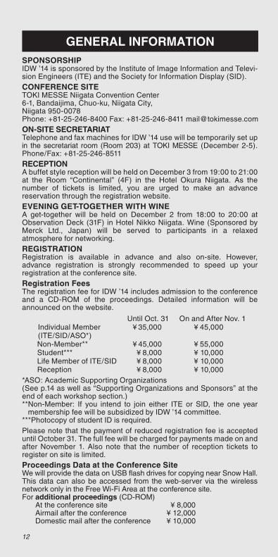
GENERAL INFORMATIONSPONSORSHIPIDW ’14 is sponsored by the Institute of Image Information and Televi-sion Engineers (ITE) and the Society for Information Display (SID).CONFERENCE SITETOKI MESSE Niigata Convention Center6-1, Bandaijima, Chuo-ku, Niigata City,Niigata 950-0078Phone: +81-25-246-8400 Fax: +81-25-246-8411 [email protected] SECRETARIATTelephone and fax machines for IDW ’14 use will be temporarily set up in the secretariat room (Room 203) at TOKI MESSE (December 2-5). Phone/Fax: +81-25-246-8511RECEPTIONA buffet style reception will be held on December 3 from 19:00 to 21:00 at the Room “Continental” (4F) in the Hotel Okura Niigata. As the number of tickets is limited, you are urged to make an advance reservation through the registration website.EVENING GET-TOGETHER WITH WINEA get-together will be held on December 2 from 18:00 to 20:00 at Observation Deck (31F) in Hotel Nikko Niigata. Wine (Sponsored by Merck Ltd., Japan) will be served to participants in a relaxed atmosphere for networking.REGISTRATIONRegistration is available in advance and also on-site. However, advance registration is strongly recommended to speed up your registration at the conference site.Registration FeesThe registration fee for IDW ’14 includes admission to the conference and a CD-ROM of the proceedings. Detailed information will be announced on the website.
Until Oct. 31 On and After Nov. 1Individual Member ¥ 35,000 ¥ 45,000(ITE/SID/ASO*)Non-Member** ¥ 45,000 ¥ 55,000Student*** ¥ 8,000 ¥ 10,000Life Member of ITE/SID ¥ 8,000 ¥ 10,000Reception ¥ 8,000 ¥ 10,000
*ASO: Academic Supporting Organizations(See p.14 as well as “Supporting Organizations and Sponsors” at the end of each workshop section.)**Non-Member: If you intend to join either ITE or SID, the one year
membership fee will be subsidized by IDW ’14 committee.***Photocopy of student ID is required.Please note that the payment of reduced registration fee is accepted until October 31. The full fee will be charged for payments made on and after November 1. Also note that the number of reception tickets to register on site is limited.Proceedings Data at the Conference SiteWe will provide the data on USB flash drives for copying near Snow Hall. This data can also be accessed from the web-server via the wireless network only in the Free Wi-Fi Area at the conference site.For additional proceedings (CD-ROM)
At the conference site ¥ 8,000Airmail after the conference ¥ 12,000Domestic mail after the conference ¥ 10,000
12

PaymentThree ways are provided for registration.
(1) e-RegistrationAccess the following URL. http://www.idw.or.jp/regist.htmle-Registration will be accepted until November 21, 2014.
(2) Mail or Fax RegistrationComplete the registration form (download from the website) and send itto the secretariat together with the proof of payment no later than November 21, 2014.
IDW ’14 Secretariatc/o Bilingual Group Ltd.3-3-6 Kudan Minami, Chiyoda-ku, Tokyo 102-0074, JapanPhone: +81-3-3263-1345 Fax: +81-3-3263-1264E-mail: [email protected]
The registration fee should be paid by one of the following methods.1. Credit Card (VISA, MasterCard, JCB, AMEX or Diners)2. Bank Transfer to: Bank: Bank of Tokyo-Mitsubishi UFJ (Swift Code: BOTKJPJT) Branch: Ichigaya Branch (Branch No. 14) Account No.: 0167640 (Ordinary Account) Account: IDWPlease attach a copy of the bank receipt to the registration form to avoid any confusion. Please note that the remittance charges, including that of Bank of Tokyo Mitsubishi UFJ, should be paid by the payer.
All above payments should be made in JAPANESE YEN.Also, please note that personal and traveler’s checks are not accepted.
(3) On-site RegistrationConference registration desk will open:
December 2 (Tue.) 17:00 – 20:00December 3 (Wed.) 8:00 – 18:00December 4 (Thu.) 8:00 – 18:00December 5 (Fri.) 8:00 – 13:00
On-site registration fee will be payable by:1. Cash (JAPANESE YEN only)2. Credit Card (VISA, MasterCard, JCB, AMEX, China Union Pay)
Bank transfer, bank checks, or personal/traveler’s checks are not accepted.
Cancellation PolicyUntil October 31, cancellation is accepted by writing to IDW ’14 Secre-tariat to get refunds for registration and reception. For cancellations received on and after November 1 or no-shows, refunds will not be made. However, after IDW ’14 closes, a CD-ROM of the proceedings will be sent to the registrants who have paid the registration fees. If it becomes difficult to hold IDW ’14 due to the outbreak of infectious diseases and other unavoidable factors, we will substitute the IDW with the mail delivery of the IDW ’14 proceedings at a later date to all those who have registered and completed payment.
INQUIRIESIDW ’14 Secretariatc/o Bilingual Group Ltd.3-3-6 Kudan Minami, Chiyoda-ku, Tokyo 102-0074, JapanPhone:+81-3-3263-1345 Fax: +81-3-3263-1264E-mail: [email protected]
ACADEMIC SUPPORTING ORGANIZATIONS (ASO)• The Chemical Society of Japan• The Electrochemical Society of Japan• The Illuminating Engineering Institute of Japan• The Imaging Society of Japan• The Institute of Electrical Engineers of Japan• The Institute of Electronics, Information and Communication Engineers• The Institute of Image Electronics Engineers of Japan• International Electrotechnical Commission• Japan Ergonomics Society• The Japanese Liquid Crystal Society• The Japan Society of Applied Physics• The Society of Polymer Science, Japan• The Virtual Reality Society of Japan
FUNDS• Niigata Prefectural Government• Niigata Visitors & Convention Bureau (Niigata City)• The Murata Science Foundation• Support Center for Advanced Telecommunications Technology Research, Foundation
For final updated information, please visit our website,http://www.idw.or.jp/
GENERAL INFORMATIONSPONSORSHIPIDW ’14 is sponsored by the Institute of Image Information and Televi-sion Engineers (ITE) and the Society for Information Display (SID).CONFERENCE SITETOKI MESSE Niigata Convention Center6-1, Bandaijima, Chuo-ku, Niigata City,Niigata 950-0078Phone: +81-25-246-8400 Fax: +81-25-246-8411 [email protected] SECRETARIATTelephone and fax machines for IDW ’14 use will be temporarily set up in the secretariat room (Room 203) at TOKI MESSE (December 2-5). Phone/Fax: +81-25-246-8511RECEPTIONA buffet style reception will be held on December 3 from 19:00 to 21:00 at the Room “Continental” (4F) in the Hotel Okura Niigata. As the number of tickets is limited, you are urged to make an advance reservation through the registration website.EVENING GET-TOGETHER WITH WINEA get-together will be held on December 2 from 18:00 to 20:00 at Observation Deck (31F) in Hotel Nikko Niigata. Wine (Sponsored by Merck Ltd., Japan) will be served to participants in a relaxed atmosphere for networking.REGISTRATIONRegistration is available in advance and also on-site. However, advance registration is strongly recommended to speed up your registration at the conference site.Registration FeesThe registration fee for IDW ’14 includes admission to the conference and a CD-ROM of the proceedings. Detailed information will be announced on the website.
Until Oct. 31 On and After Nov. 1Individual Member ¥ 35,000 ¥ 45,000(ITE/SID/ASO*)Non-Member** ¥ 45,000 ¥ 55,000Student*** ¥ 8,000 ¥ 10,000Life Member of ITE/SID ¥ 8,000 ¥ 10,000Reception ¥ 8,000 ¥ 10,000
*ASO: Academic Supporting Organizations(See p.14 as well as “Supporting Organizations and Sponsors” at the end of each workshop section.)**Non-Member: If you intend to join either ITE or SID, the one year
membership fee will be subsidized by IDW ’14 committee.***Photocopy of student ID is required.Please note that the payment of reduced registration fee is accepted until October 31. The full fee will be charged for payments made on and after November 1. Also note that the number of reception tickets to register on site is limited.Proceedings Data at the Conference SiteWe will provide the data on USB flash drives for copying near Snow Hall. This data can also be accessed from the web-server via the wireless network only in the Free Wi-Fi Area at the conference site.For additional proceedings (CD-ROM)
At the conference site ¥ 8,000Airmail after the conference ¥ 12,000Domestic mail after the conference ¥ 10,000
13

ACCOMMODATIONSJTB Kanto Corp. will handle arrangements for your hotel reservations.
Hotel reservations can be made at the IDW website.http://www.idw.or.jp/accommodation.html
Hotel list and the rates are available on the Pullout of this Advance Program.
JTB Kanto Corp.Corporate Sales Division, Niigata, IDW ’14 Desk
Phone: +81-25-255-5101 Fax: +81-25-248-7687Office Hours: 9:30-17:30 (Weekdays only)E-mail: [email protected]
There will be an on-site travel information desk during the conference period to handle arrangements for transportations.
VISASVisitors from countries whose citizens must have visas should apply to Japanese consular office or diplomatic mission in their respective countries. For further details, please contact your travel agency or the local consular office in your country.Attention: For some countries’ citizens, official documents prepared by the secretariat will be needed. Please access the IDW website for applications.http://www.idw.or.jp/visa.html
JAPAN RAIL PASS AND JR EAST PASSJapan Railway (JR) provides the following economical passes. They should be purchased before you leave your country. Please contact your travel agency. Visit following sites for the details.(1) The JAPAN RAIL PASS is the most economical way to travelthroughout Japan by rail and JR buses.(2) The JR EAST PASS is an economical and flexible rail pass to travelaround Eastern Japan.Japan Rail Pass: http://www.japanrailpass.net/eng/en001.htmlJR East Pass: http://www.jreast.co.jp/e/eastpass/
CLIMATEThe average temperature in Niigata during the conference should be around 9°C (48°F) in the daytime and 3°C (37°F) at night.
NIIGATA CITYNiigata City is located in the center of the Japanese Islands, 250 km north of Tokyo. The city has a long history as a port, and is distinguished for being the site of one of only five international ports opened in 1868 when Japan resumed contact with other countries after nearly 250 years of isolation. Since that time, Niigata has developed into one of the most important modern international ports in Japan. Geographically, the city is distinctive in that it is surrounded by water. The Shinano and Agano, two of the largest rivers in Japan, run through the heart of Niigata before emptying into the sea. Until relatively recently, the city was also crisscrossed by a series of canals used to transport goods. Although the canals have been filled in to make the construction of modern roadways possible, the willows that lined these canals still remain today and now serve to lend a gentle air to the bustling downtown area.When Niigata is mentioned, many people often think of the area’s delicious rice and sake or the city’s beautiful sunsets. But the residents of Niigata themselves take pride, rather, in the spirit of hospitality and community that so distinguishes the city.
PLACES OF INTERESTSado IslandSado Island lies isolated from the mainland by 35 km, and is accessible by Sado Kisen, a ferry service from Niigata City which takes two and a half hours by car ferry or only one hour by jet foil. Sado Island has a perimeter of 261 km, and a total area of 855.26 km2. It is one of the largest islands in Japan. Many tourists come from all over the country every year to visit Sado, an island rich in natural beauty and historic monuments.Niigata FurusatomuraThis facility displays and provides information relating to Niigata’s history, culture and sightseeing spots. There are shops selling various traditional crafts and local products, such as sake, rice and fish, for which Niigata is famous throughout the country. In addition, there is a food court serving delicious local dishes. http://furusatomura.pref.niigata.jp/modules/guide09/index.php?id=2Bandai BridgeThe present Bandai Bridge is the third to have spanned the Shinano River (the first was built in 1887, the second in 1909 and the third in 1929). The bridge is 307 m long, 21.9 m wide and consists of 6 arches. Not only was it strong enough to survive the Niigata Earthquake during the 1960s, it has also become one of the symbols of Niigata City.Prefectural Government Memorial HallBuilt in 1884, this building was formerly home to the Niigata Prefectural Assembly. This Western-style building fuses elements of Western and traditional Japanese architecture. It is the only prefectural assembly building dating from the early Meiji era (1868~1912) still in existence in Japan and is designated as a nationally important cultural property.The hall is located in Hakusan Park; 10-minute bus ride from Niigata station.NIIGATA INFORMATION DESKInformation concerning hotels and tours will be available during the conference period. More information is available from these websites:(Niigata City Online) http://www.city.niigata.lg.jp/multilingual/e_index/index.htmlNiigata Prefecture Tourism Guideenjoyniigata.com
TRAVEL INFORMATIONPaymentThree ways are provided for registration.
(1) e-RegistrationAccess the following URL. http://www.idw.or.jp/regist.htmle-Registration will be accepted until November 21, 2014.
(2) Mail or Fax RegistrationComplete the registration form (download from the website) and send itto the secretariat together with the proof of payment no later than November 21, 2014.
IDW ’14 Secretariatc/o Bilingual Group Ltd.3-3-6 Kudan Minami, Chiyoda-ku, Tokyo 102-0074, JapanPhone: +81-3-3263-1345 Fax: +81-3-3263-1264E-mail: [email protected]
The registration fee should be paid by one of the following methods.1. Credit Card (VISA, MasterCard, JCB, AMEX or Diners)2. Bank Transfer to: Bank: Bank of Tokyo-Mitsubishi UFJ (Swift Code: BOTKJPJT) Branch: Ichigaya Branch (Branch No. 14) Account No.: 0167640 (Ordinary Account) Account: IDWPlease attach a copy of the bank receipt to the registration form to avoid any confusion. Please note that the remittance charges, including that of Bank of Tokyo Mitsubishi UFJ, should be paid by the payer.
All above payments should be made in JAPANESE YEN.Also, please note that personal and traveler’s checks are not accepted.
(3) On-site RegistrationConference registration desk will open:
December 2 (Tue.) 17:00 – 20:00December 3 (Wed.) 8:00 – 18:00December 4 (Thu.) 8:00 – 18:00December 5 (Fri.) 8:00 – 13:00
On-site registration fee will be payable by:1. Cash (JAPANESE YEN only)2. Credit Card (VISA, MasterCard, JCB, AMEX, China Union Pay)
Bank transfer, bank checks, or personal/traveler’s checks are not accepted.
Cancellation PolicyUntil October 31, cancellation is accepted by writing to IDW ’14 Secre-tariat to get refunds for registration and reception. For cancellations received on and after November 1 or no-shows, refunds will not be made. However, after IDW ’14 closes, a CD-ROM of the proceedings will be sent to the registrants who have paid the registration fees. If it becomes difficult to hold IDW ’14 due to the outbreak of infectious diseases and other unavoidable factors, we will substitute the IDW with the mail delivery of the IDW ’14 proceedings at a later date to all those who have registered and completed payment.
INQUIRIESIDW ’14 Secretariatc/o Bilingual Group Ltd.3-3-6 Kudan Minami, Chiyoda-ku, Tokyo 102-0074, JapanPhone:+81-3-3263-1345 Fax: +81-3-3263-1264E-mail: [email protected]
ACADEMIC SUPPORTING ORGANIZATIONS (ASO)• The Chemical Society of Japan• The Electrochemical Society of Japan• The Illuminating Engineering Institute of Japan• The Imaging Society of Japan• The Institute of Electrical Engineers of Japan• The Institute of Electronics, Information and Communication Engineers• The Institute of Image Electronics Engineers of Japan• International Electrotechnical Commission• Japan Ergonomics Society• The Japanese Liquid Crystal Society• The Japan Society of Applied Physics• The Society of Polymer Science, Japan• The Virtual Reality Society of Japan
FUNDS• Niigata Prefectural Government• Niigata Visitors & Convention Bureau (Niigata City)• The Murata Science Foundation• Support Center for Advanced Telecommunications Technology Research, Foundation
For final updated information, please visit our website,http://www.idw.or.jp/
14

ACCOMMODATIONSJTB Kanto Corp. will handle arrangements for your hotel reservations.
Hotel reservations can be made at the IDW website.http://www.idw.or.jp/accommodation.html
Hotel list and the rates are available on the Pullout of this Advance Program.
JTB Kanto Corp.Corporate Sales Division, Niigata, IDW ’14 Desk
Phone: +81-25-255-5101 Fax: +81-25-248-7687Office Hours: 9:30-17:30 (Weekdays only)E-mail: [email protected]
There will be an on-site travel information desk during the conference period to handle arrangements for transportations.
VISASVisitors from countries whose citizens must have visas should apply to Japanese consular office or diplomatic mission in their respective countries. For further details, please contact your travel agency or the local consular office in your country.Attention: For some countries’ citizens, official documents prepared by the secretariat will be needed. Please access the IDW website for applications.http://www.idw.or.jp/visa.html
JAPAN RAIL PASS AND JR EAST PASSJapan Railway (JR) provides the following economical passes. They should be purchased before you leave your country. Please contact your travel agency. Visit following sites for the details.(1) The JAPAN RAIL PASS is the most economical way to travelthroughout Japan by rail and JR buses.(2) The JR EAST PASS is an economical and flexible rail pass to travelaround Eastern Japan.Japan Rail Pass: http://www.japanrailpass.net/eng/en001.htmlJR East Pass: http://www.jreast.co.jp/e/eastpass/
CLIMATEThe average temperature in Niigata during the conference should be around 9°C (48°F) in the daytime and 3°C (37°F) at night.
NIIGATA CITYNiigata City is located in the center of the Japanese Islands, 250 km north of Tokyo. The city has a long history as a port, and is distinguished for being the site of one of only five international ports opened in 1868 when Japan resumed contact with other countries after nearly 250 years of isolation. Since that time, Niigata has developed into one of the most important modern international ports in Japan. Geographically, the city is distinctive in that it is surrounded by water. The Shinano and Agano, two of the largest rivers in Japan, run through the heart of Niigata before emptying into the sea. Until relatively recently, the city was also crisscrossed by a series of canals used to transport goods. Although the canals have been filled in to make the construction of modern roadways possible, the willows that lined these canals still remain today and now serve to lend a gentle air to the bustling downtown area.When Niigata is mentioned, many people often think of the area’s delicious rice and sake or the city’s beautiful sunsets. But the residents of Niigata themselves take pride, rather, in the spirit of hospitality and community that so distinguishes the city.
PLACES OF INTERESTSado IslandSado Island lies isolated from the mainland by 35 km, and is accessible by Sado Kisen, a ferry service from Niigata City which takes two and a half hours by car ferry or only one hour by jet foil. Sado Island has a perimeter of 261 km, and a total area of 855.26 km2. It is one of the largest islands in Japan. Many tourists come from all over the country every year to visit Sado, an island rich in natural beauty and historic monuments.Niigata FurusatomuraThis facility displays and provides information relating to Niigata’s history, culture and sightseeing spots. There are shops selling various traditional crafts and local products, such as sake, rice and fish, for which Niigata is famous throughout the country. In addition, there is a food court serving delicious local dishes. http://furusatomura.pref.niigata.jp/modules/guide09/index.php?id=2Bandai BridgeThe present Bandai Bridge is the third to have spanned the Shinano River (the first was built in 1887, the second in 1909 and the third in 1929). The bridge is 307 m long, 21.9 m wide and consists of 6 arches. Not only was it strong enough to survive the Niigata Earthquake during the 1960s, it has also become one of the symbols of Niigata City.Prefectural Government Memorial HallBuilt in 1884, this building was formerly home to the Niigata Prefectural Assembly. This Western-style building fuses elements of Western and traditional Japanese architecture. It is the only prefectural assembly building dating from the early Meiji era (1868~1912) still in existence in Japan and is designated as a nationally important cultural property.The hall is located in Hakusan Park; 10-minute bus ride from Niigata station.NIIGATA INFORMATION DESKInformation concerning hotels and tours will be available during the conference period. More information is available from these websites:(Niigata City Online) http://www.city.niigata.lg.jp/multilingual/e_index/index.htmlNiigata Prefecture Tourism Guideenjoyniigata.com
TRAVEL INFORMATIONPaymentThree ways are provided for registration.
(1) e-RegistrationAccess the following URL. http://www.idw.or.jp/regist.htmle-Registration will be accepted until November 21, 2014.
(2) Mail or Fax RegistrationComplete the registration form (download from the website) and send itto the secretariat together with the proof of payment no later than November 21, 2014.
IDW ’14 Secretariatc/o Bilingual Group Ltd.3-3-6 Kudan Minami, Chiyoda-ku, Tokyo 102-0074, JapanPhone: +81-3-3263-1345 Fax: +81-3-3263-1264E-mail: [email protected]
The registration fee should be paid by one of the following methods.1. Credit Card (VISA, MasterCard, JCB, AMEX or Diners)2. Bank Transfer to: Bank: Bank of Tokyo-Mitsubishi UFJ (Swift Code: BOTKJPJT) Branch: Ichigaya Branch (Branch No. 14) Account No.: 0167640 (Ordinary Account) Account: IDWPlease attach a copy of the bank receipt to the registration form to avoid any confusion. Please note that the remittance charges, including that of Bank of Tokyo Mitsubishi UFJ, should be paid by the payer.
All above payments should be made in JAPANESE YEN.Also, please note that personal and traveler’s checks are not accepted.
(3) On-site RegistrationConference registration desk will open:
December 2 (Tue.) 17:00 – 20:00December 3 (Wed.) 8:00 – 18:00December 4 (Thu.) 8:00 – 18:00December 5 (Fri.) 8:00 – 13:00
On-site registration fee will be payable by:1. Cash (JAPANESE YEN only)2. Credit Card (VISA, MasterCard, JCB, AMEX, China Union Pay)
Bank transfer, bank checks, or personal/traveler’s checks are not accepted.
Cancellation PolicyUntil October 31, cancellation is accepted by writing to IDW ’14 Secre-tariat to get refunds for registration and reception. For cancellations received on and after November 1 or no-shows, refunds will not be made. However, after IDW ’14 closes, a CD-ROM of the proceedings will be sent to the registrants who have paid the registration fees. If it becomes difficult to hold IDW ’14 due to the outbreak of infectious diseases and other unavoidable factors, we will substitute the IDW with the mail delivery of the IDW ’14 proceedings at a later date to all those who have registered and completed payment.
INQUIRIESIDW ’14 Secretariatc/o Bilingual Group Ltd.3-3-6 Kudan Minami, Chiyoda-ku, Tokyo 102-0074, JapanPhone:+81-3-3263-1345 Fax: +81-3-3263-1264E-mail: [email protected]
ACADEMIC SUPPORTING ORGANIZATIONS (ASO)• The Chemical Society of Japan• The Electrochemical Society of Japan• The Illuminating Engineering Institute of Japan• The Imaging Society of Japan• The Institute of Electrical Engineers of Japan• The Institute of Electronics, Information and Communication Engineers• The Institute of Image Electronics Engineers of Japan• International Electrotechnical Commission• Japan Ergonomics Society• The Japanese Liquid Crystal Society• The Japan Society of Applied Physics• The Society of Polymer Science, Japan• The Virtual Reality Society of Japan
FUNDS• Niigata Prefectural Government• Niigata Visitors & Convention Bureau (Niigata City)• The Murata Science Foundation• Support Center for Advanced Telecommunications Technology Research, Foundation
For final updated information, please visit our website,http://www.idw.or.jp/
15

ACCOMMODATIONSJTB Kanto Corp. will handle arrangements for your hotel reservations.
Hotel reservations can be made at the IDW website.http://www.idw.or.jp/accommodation.html
Hotel list and the rates are available on the Pullout of this Advance Program.
JTB Kanto Corp.Corporate Sales Division, Niigata, IDW ’14 Desk
Phone: +81-25-255-5101 Fax: +81-25-248-7687Office Hours: 9:30-17:30 (Weekdays only)E-mail: [email protected]
There will be an on-site travel information desk during the conference period to handle arrangements for transportations.
VISASVisitors from countries whose citizens must have visas should apply to Japanese consular office or diplomatic mission in their respective countries. For further details, please contact your travel agency or the local consular office in your country.Attention: For some countries’ citizens, official documents prepared by the secretariat will be needed. Please access the IDW website for applications.http://www.idw.or.jp/visa.html
JAPAN RAIL PASS AND JR EAST PASSJapan Railway (JR) provides the following economical passes. They should be purchased before you leave your country. Please contact your travel agency. Visit following sites for the details.(1) The JAPAN RAIL PASS is the most economical way to travelthroughout Japan by rail and JR buses.(2) The JR EAST PASS is an economical and flexible rail pass to travelaround Eastern Japan.Japan Rail Pass: http://www.japanrailpass.net/eng/en001.htmlJR East Pass: http://www.jreast.co.jp/e/eastpass/
CLIMATEThe average temperature in Niigata during the conference should be around 9°C (48°F) in the daytime and 3°C (37°F) at night.
NIIGATA CITYNiigata City is located in the center of the Japanese Islands, 250 km north of Tokyo. The city has a long history as a port, and is distinguished for being the site of one of only five international ports opened in 1868 when Japan resumed contact with other countries after nearly 250 years of isolation. Since that time, Niigata has developed into one of the most important modern international ports in Japan. Geographically, the city is distinctive in that it is surrounded by water. The Shinano and Agano, two of the largest rivers in Japan, run through the heart of Niigata before emptying into the sea. Until relatively recently, the city was also crisscrossed by a series of canals used to transport goods. Although the canals have been filled in to make the construction of modern roadways possible, the willows that lined these canals still remain today and now serve to lend a gentle air to the bustling downtown area.When Niigata is mentioned, many people often think of the area’s delicious rice and sake or the city’s beautiful sunsets. But the residents of Niigata themselves take pride, rather, in the spirit of hospitality and community that so distinguishes the city.
PLACES OF INTERESTSado IslandSado Island lies isolated from the mainland by 35 km, and is accessible by Sado Kisen, a ferry service from Niigata City which takes two and a half hours by car ferry or only one hour by jet foil. Sado Island has a perimeter of 261 km, and a total area of 855.26 km2. It is one of the largest islands in Japan. Many tourists come from all over the country every year to visit Sado, an island rich in natural beauty and historic monuments.Niigata FurusatomuraThis facility displays and provides information relating to Niigata’s history, culture and sightseeing spots. There are shops selling various traditional crafts and local products, such as sake, rice and fish, for which Niigata is famous throughout the country. In addition, there is a food court serving delicious local dishes. http://furusatomura.pref.niigata.jp/modules/guide09/index.php?id=2Bandai BridgeThe present Bandai Bridge is the third to have spanned the Shinano River (the first was built in 1887, the second in 1909 and the third in 1929). The bridge is 307 m long, 21.9 m wide and consists of 6 arches. Not only was it strong enough to survive the Niigata Earthquake during the 1960s, it has also become one of the symbols of Niigata City.Prefectural Government Memorial HallBuilt in 1884, this building was formerly home to the Niigata Prefectural Assembly. This Western-style building fuses elements of Western and traditional Japanese architecture. It is the only prefectural assembly building dating from the early Meiji era (1868~1912) still in existence in Japan and is designated as a nationally important cultural property.The hall is located in Hakusan Park; 10-minute bus ride from Niigata station.NIIGATA INFORMATION DESKInformation concerning hotels and tours will be available during the conference period. More information is available from these websites:(Niigata City Online) http://www.city.niigata.lg.jp/multilingual/e_index/index.htmlNiigata Prefecture Tourism Guideenjoyniigata.com
TRAVEL INFORMATION
16

ACCOMMODATIONSJTB Kanto Corp. will handle arrangements for your hotel reservations.
Hotel reservations can be made at the IDW website.http://www.idw.or.jp/accommodation.html
Hotel list and the rates are available on the Pullout of this Advance Program.
JTB Kanto Corp.Corporate Sales Division, Niigata, IDW ’14 Desk
Phone: +81-25-255-5101 Fax: +81-25-248-7687Office Hours: 9:30-17:30 (Weekdays only)E-mail: [email protected]
There will be an on-site travel information desk during the conference period to handle arrangements for transportations.
VISASVisitors from countries whose citizens must have visas should apply to Japanese consular office or diplomatic mission in their respective countries. For further details, please contact your travel agency or the local consular office in your country.Attention: For some countries’ citizens, official documents prepared by the secretariat will be needed. Please access the IDW website for applications.http://www.idw.or.jp/visa.html
JAPAN RAIL PASS AND JR EAST PASSJapan Railway (JR) provides the following economical passes. They should be purchased before you leave your country. Please contact your travel agency. Visit following sites for the details.(1) The JAPAN RAIL PASS is the most economical way to travelthroughout Japan by rail and JR buses.(2) The JR EAST PASS is an economical and flexible rail pass to travelaround Eastern Japan.Japan Rail Pass: http://www.japanrailpass.net/eng/en001.htmlJR East Pass: http://www.jreast.co.jp/e/eastpass/
CLIMATEThe average temperature in Niigata during the conference should be around 9°C (48°F) in the daytime and 3°C (37°F) at night.
NIIGATA CITYNiigata City is located in the center of the Japanese Islands, 250 km north of Tokyo. The city has a long history as a port, and is distinguished for being the site of one of only five international ports opened in 1868 when Japan resumed contact with other countries after nearly 250 years of isolation. Since that time, Niigata has developed into one of the most important modern international ports in Japan. Geographically, the city is distinctive in that it is surrounded by water. The Shinano and Agano, two of the largest rivers in Japan, run through the heart of Niigata before emptying into the sea. Until relatively recently, the city was also crisscrossed by a series of canals used to transport goods. Although the canals have been filled in to make the construction of modern roadways possible, the willows that lined these canals still remain today and now serve to lend a gentle air to the bustling downtown area.When Niigata is mentioned, many people often think of the area’s delicious rice and sake or the city’s beautiful sunsets. But the residents of Niigata themselves take pride, rather, in the spirit of hospitality and community that so distinguishes the city.
PLACES OF INTERESTSado IslandSado Island lies isolated from the mainland by 35 km, and is accessible by Sado Kisen, a ferry service from Niigata City which takes two and a half hours by car ferry or only one hour by jet foil. Sado Island has a perimeter of 261 km, and a total area of 855.26 km2. It is one of the largest islands in Japan. Many tourists come from all over the country every year to visit Sado, an island rich in natural beauty and historic monuments.Niigata FurusatomuraThis facility displays and provides information relating to Niigata’s history, culture and sightseeing spots. There are shops selling various traditional crafts and local products, such as sake, rice and fish, for which Niigata is famous throughout the country. In addition, there is a food court serving delicious local dishes. http://furusatomura.pref.niigata.jp/modules/guide09/index.php?id=2Bandai BridgeThe present Bandai Bridge is the third to have spanned the Shinano River (the first was built in 1887, the second in 1909 and the third in 1929). The bridge is 307 m long, 21.9 m wide and consists of 6 arches. Not only was it strong enough to survive the Niigata Earthquake during the 1960s, it has also become one of the symbols of Niigata City.Prefectural Government Memorial HallBuilt in 1884, this building was formerly home to the Niigata Prefectural Assembly. This Western-style building fuses elements of Western and traditional Japanese architecture. It is the only prefectural assembly building dating from the early Meiji era (1868~1912) still in existence in Japan and is designated as a nationally important cultural property.The hall is located in Hakusan Park; 10-minute bus ride from Niigata station.NIIGATA INFORMATION DESKInformation concerning hotels and tours will be available during the conference period. More information is available from these websites:(Niigata City Online) http://www.city.niigata.lg.jp/multilingual/e_index/index.htmlNiigata Prefecture Tourism Guideenjoyniigata.com
TRAVEL INFORMATION Access to Conference Site
Shin-OsakaStation
JR Narita Exp.56 min.
Tokyo Station
(as of July, 2014)
Narita Int'lAirport(NRT)
Kansai Int'lAirport(KIX)
NagoyaChubu Centrair
Int'l Airport (NGO)
Bus¥ 1,950 / 75 min.JR Haruka Exp.
50 min.
Osaka int'lAirport
Itami (ITM)
JR TokaidoShinkansen Nozomi
153 min.
Flight 65 min.10 flights / day
SapporoHarbin, ChinaShanghai, China etc.
Int'l flight 115 min.2 flights / day
Niigata Airport (KIJ)
Taxi¥ 3,000 / 25 min.
Taxi¥ 1,000 / 5 min.
Bus¥ 410 / 25 min.
Bus¥ 410 / 30 min.
JR JoetsuShinkansen Toki
115 min.
Bus¥ 210 / 15 min.
Bus¥ 210 / 5-10 min.
TOKI MESSE Niigata Convention Center
Taxi¥ 2,000-3,000
/ 20 min.
Bandai City Bus Center
Flight 60 min.2 flights / day
Niigata Station
¥ 13,050 from Narita Int'l Airport¥ 23,100 from Kansai Int'l Airport
Incheon Int'lAirport, Korea
(ICN)
15 min.on foot
17

Niigata Downtown and Hotel Locations
500 mBus route No.17
* Only buses from Toki Messe stop.
① Hotel Nikko Niigata② ANA Crowne Plaza Hotel③ Bandai Silver Hotel④ Hotel Okura Niigata⑤ Niigata Grand Hotel⑥ Niigata Tokyu Inn⑦ Hotel Sanroute Niigata⑧ Niigata Toei Hotel⑨ Court Hotel Niigata⑩ Comfort Hotel Niigata
Toki Messe
N
Sado KisenFerry Terminal
Bandai Bridge
Bandai CityBus Center
(Gate 6)
Shokugyo Anteisho Mae
JR Niigata StationBandai Exit
Niigata Eki Mae(Bus Terminal)
Ekimae Doori*
JR Echigo Line
Joetsu Shinkansen
Tokyo
Conference SiteToki Messe
Niigata Convention Center
Ryuto Bridge
Shin
ano
Riv
er
Gate 5: 17 Sado Kisen (via Toki Messe)Gate 6: 331 Niigata Airport
Phone: +81-25-240-1888Phone: +81-25-245-3333Phone: +81-25-243-3711Phone: +81-25-224-6111Phone: +81-25-228-6111Phone: +81-25-243-0109Phone: +81-25-246-6161Phone: +81-25-244-7101Phone: +81-25-247-0505Phone: +81-25-242-0611
Bandai City Bus Center Mae
AirportLimousine Bus Stop(Platforms)
⑩
18

Niigata Downtown and Hotel Locations
500 mBus route No.17
* Only buses from Toki Messe stop.
① Hotel Nikko Niigata② ANA Crowne Plaza Hotel③ Bandai Silver Hotel④ Hotel Okura Niigata⑤ Niigata Grand Hotel⑥ Niigata Tokyu Inn⑦ Hotel Sanroute Niigata⑧ Niigata Toei Hotel⑨ Court Hotel Niigata⑩ Comfort Hotel Niigata
Toki Messe
N
Sado KisenFerry Terminal
Bandai Bridge
Bandai CityBus Center
(Gate 6)
Shokugyo Anteisho Mae
JR Niigata StationBandai Exit
Niigata Eki Mae(Bus Terminal)
Ekimae Doori*
JR Echigo Line
Joetsu Shinkansen
Tokyo
Conference SiteToki Messe
Niigata Convention Center
Ryuto Bridge
Shin
ano
Riv
er
Gate 5: 17 Sado Kisen (via Toki Messe)Gate 6: 331 Niigata Airport
Phone: +81-25-240-1888Phone: +81-25-245-3333Phone: +81-25-243-3711Phone: +81-25-224-6111Phone: +81-25-228-6111Phone: +81-25-243-0109Phone: +81-25-246-6161Phone: +81-25-244-7101Phone: +81-25-247-0505Phone: +81-25-242-0611
Bandai City Bus Center Mae
AirportLimousine Bus Stop(Platforms)
⑩
Late-News PapersDue September 25, 2014
Submit a two-page camera-ready manuscriptvia IDW website:
http://www.idw.or.jp/latenews.html
“Innovative Demonstration Session”by Oral and Poster Presenters
Live demonstrations of emerging information display technologies
Thursday, December 4, 2014Friday, December 5, 2014
In the afternoonExhibition Hall B
Evening Get-Together with Wine
Tuesday, December 2, 201418:00 – 20:00
Observation Deck (31F),Hotel Nikko Niigata
(Sponsored by Merck Ltd., Japan)See page 12 for details
Final ProgramThe final program of IDW ’14 will be available on
the website (http://www.idw.or.jp/) from the middle of November.
19

Plenary Sessions
Wednesday, December 3
9:30 - 9:50 Snow Hall
Opening
Master of Ceremony: S. Komura, Executive Chair, Japan Display, Japan
Opening Remarks9:30
K. Azuma, General Chair, IDW
A. Ghosh, President of SID
K. Kubota, President of ITE
A. Mikami, Program Chair, IDW
9:50 - 11:10 Snow Hall
Keynote Addresses
Chair: A. Mikami, Program Chair, IDWCo-Chair: K. Azuma, General Chair, IDW
Keynote Address - 19:50
Recent Progress on 8K Super Hi-Vision
M. Sugawara
NHK, Japan
Keynote Address - 210:30
Display Technologies in Mobile Applications
J. Hong
Qualcomm, USA
----- Break -----
Wednesday December 3
IDW Best Paper Award
IDW OutstandingPoster Paper Award
These awards will go to the most outstanding papers selected from those presented at IDW ’14.
The 2014 award winners will be announced on the IDW website: http://www.idw.or.jp/award.html
20

11:20 - 12:30 Snow Hall
Invited Addresses
Chair: M. Kimura, Vice-Program Chair, IDWCo-Chair: Y. Gotoh, Vice-Program Chair, IDW
Invited Address - 111:20
Research and Development of Oxide TFTs
S.-H. K. Park
KAIST, Korea
Invited Address - 211:55
Ultraflexible Electronics Using Organic Devices
T. Someya
Univ. of Tokyo, Japan
IDW ’14 Tutorial in JapaneseOrganized by SID Japan Chapter
Tuesday, December 2, 2014Room 301, 3F
TOKI MESSE Niigata Convention Center
Detailed information is available onhttp://www.sid-japan.org
Wednesday December 3
“Innovative Demonstration Session”by Oral and Poster Presenters
Live demonstrations of emerging information display technologies
Thursday, December 4, 2014Friday, December 5, 2014
In the afternoonExhibition Hall B
21

Special Topics of Interest onOxide-Semiconductor TFT
Wednesday, December 3
14:00 - 17:00 Exhibition Hall B
Poster AMDp1: Oxide TFT
AMDp1 - 1 Influence of Subthreshold Leakage Current on Temperature Dependence of Oxide TFTs with Light-Induced Bias-Stress
B.-L. Yeh, C.-N. Lin
AU Optronics, Taiwan
AMDp1 - 2 A 31-in. FHD AMOLED TV Driven by Amorphous IGZO TFTs
H.-J. Zhang, C.-Y. Su, W.-H. Li, L.-Q. Shi, X.-W. Lv, Y.-T. Hu, C.-Y. Tseng, Y.-F. Wang, C.-C. Lo
Shenzhen China Star Optoelect. Tech., China
AMDp1 - 3 5.8-in. Indium Gallium Zinc Oxide TFT LCD with Slim Border
E.-C. Liu, Y.-H. Chen, S.-C. Chiang, Y.-J. Lu, Y.-Y. Huang
Chunghwa Picture Tubes, Taiwan
AMDp1 - 4 Investigation of Hysteresis in Dual-Gate a-IGZO TFTs
Y.-H. Kim, J. G. Um, S. Lee, M. Mativenga, J. Jang
Kyung Hee Univ., Korea
AMDp1 - 5 CVD-Free and Low Temperature a-InGaZnO TFTs for Flexible Display Applications
W.-T. Lin, C.-C. Cheng, C.-Y. Liu, M.-F. Chiang
AU Optronics, Taiwan
AMDp1 - 6 Investigation for the Time-Dependent Characteristics of Sol-Gel Processed Zinc-Tin-Oxide (ZTO) Transistors
Y. W. Wang, T. M. Jian, H. H. Wang, W. L. Liu
Nat. Chang Hua Univ. of Education, Taiwan
AMDp1 - 7 Electrical Characteristics and Stability of Bottom Gate a-InGaZnO TFTs with Different Geometric Structures
H.-W. Li, C.-P. Chang, H.-H. Lu
AU Optronics, Taiwan
Wednesday December 3
22

AMDp1 - 8 Hysteresis Improvements by Introducing a Double-Active-Layered Structure in a-InGaZnO TFTs
Y.-C. Tsai, F.-J. Chan, P.-T. Liu, H.-P. D.-D. Shieh
Nat. Chiao Tung Univ., Taiwan
AMDp1 - 9 Self Heating Induced Hole Trapping at Back-Channel Edge of Flexible a-InGaZnO TFTs under Gate and Drain Bias Stress
G. Li*, B.-R. Yang*,**, Y.-C. Tsai***, R. Zhan*, C.-Y. Su****, C.-Y. Lee****, C.-Y. Tseng****, C.-C. Lo****, A. Lien*****, S. Deng*, N. Xu*, H.-P. D.-D. Shieh***
*Nat. Sun Yat-Sen Univ., China **SYSU-CMU Shunde Int. Joint Res. Inst., China ***Nat. Chiao Tung Univ., Taiwan ****Shenzhen China Star Optoelect. Tech., China *****TCL Corporate Res., China
AMDp1 - 10 Enhancement of Performance and Storage Stability of Thin-Film Transistor with InZnSnO/InGaZnO Bilayer Stack Channel Layers
P.-T. Liu, C.-S. Fuh, C.-H. Chang, C.-C. Chang, X.-Y. Yeh
Nat. Chiao Tung Univ., Taiwan
AMDp1 - 11 Effects of Negative-Gate-Bias with Illumination Stress on the Hysteresis in the Transfer Curve of a-IGZO TFT Measured by the New Sampling Method
Y.-J. Chen, Z.-H. Cai, Y.-H. Tai, C.-Y. Chang, C.-J. Li*, Y.-H. Yeh*
Nat. Chiao Tung Univ., Taiwan *ITRI, Taiwan
AMDp1 - 12 Back-Channel-Etching (BCE) TFT Fabrication with High Etchant-Resistive Solute Metal Oxide Semiconductor
K.-H. Su, M. Marinkovic, D.-V. Pham, A. Merkulov, A. Hoppe, R. Anselmann
Evonik Inds., Germany
AMDp1 - 13 Reduction of Hysteresis in Transfer Characteristics of Solution Processed IZTO TFT by Plasma Treatment
T.-H. Kim, C. Avis, H.-R. Hwang, J. Jang
Kyung Hee Univ., Korea
AMDp1 - 14 Effect of Solution Processed AlOX Passivation on Back Channel Etch a-IGZO TFTs
S. An, M. Mativenga, X. Lee, J. Jang
Kyung Hee Univ., Korea
Wednesday December 3
23

AMDp1 - 15 Impact of Negative Bias and Illumination Stress on Channel and Series Resistance of Back Channel Etched a-IGZO TFTs
M. Chun, J. Um, M. Mativenga, J. Jang
Kyung Hee Univ., Korea
Thursday, December 4
9:00 - 10:15 Snow Hall A
AMD1: High Resolution Displays Using LTPS and Oxide TFTs
Chair: T. Kamiya, Tokyo Inst. of Tech., JapanCo-Chair: K. Takatori, NLT Techs., Japan
AMD1 - 1:9:00
Invited High PPI Technologies for Mobile Displays
A. Takimoto
Japan Display, Japan
AMD1 - 2:9:25
Invited Advantages of IGZO Platform in Ultra-High-Resolution LCD Applications
N. Ueda, Y. Ogawa, K. Okada, A. Oda, S. Katoh, S. Uchida, K. Yamamoto, T. Matsuo, H. Kawamori
Sharp, Japan
AMD1 - 3:9:50
Invited Ultra High-Definition OLED Display Using C-Axis Aligned Crystalline Oxide Semiconductor FETs
H. Miyake, S. Kawashima, S. Inoue, M. Shiokawa, A. Suzuki, S. Eguchi, Y. Hirakata, J. Koyama, S. Yamazaki, T. Sato*, T. Shigenobu*, Y. Ohta**, S. Mitsui**, N. Ueda**, T. Matsuo**
Semiconductor Energy Lab., Japan *Advanced Film Device, Japan **Sharp, Japan
9:00 - 12:00 Exhibition Hall B
Poster FMCp4: Oxide TFT/Printed Electronics
FMCp4 - 1 Effect of Cu Dopant on Structural and Optical Properties of Zinc Oxide Nanorods
Z. Jin, T. Umakoshi, Y. Abe, M. Kawamura, K. H. Kim
Kitami Inst. of Tech., Japan
FMCp4 - 2 Post-Annealing Effect of Zinc Oxide Nanorods Grown on Al-Doped Zinc Oxide Seed Layers
T. Umakoshi, Y. Abe, M. Kawamura, K. H. Kim
Kitami Inst. of Tech., Japan
Wed./Thu. December 3/4
24

FMCp4 - 3 Application of Microwave-Detected Photoconductivity Decay Technique to Process Monitoring in Back Channel Etching-Type TFT Fabrication
H. Goto, M. Ochi, H. Tao, S. Morita, Y. Takanashi, A. Hino, K. Hayashi, T. Kugimiya
Kobe Steel, Japan
FMCp4 - 4 Copper Nano Particle Ink for Reverse Offset Printing and the Application to Thin Film Transistors
M. Koutake*,**
*JAPERA, Japan **DIC, Japan
10:45 - 12:20 Snow Hall A
AMD2: Physics of Oxide Semiconductors
Chair: J. Jang, Kyung Hee Univ., KoreaCo-Chair: N. Morosawa, Sony, Japan
AMD2 - 1:10:45
Invited Multiple Origins of Near-VBM Defects and Its Passivation Effects in Amorphous In-Ga-Zn-O
T. Kamiya, H. Kumomi, H. Hosono
Tokyo Inst. of Tech., Japan
AMD2 - 2:11:10
Invited Thermalization Energy Analysis of the Stability of Amorphous Oxide Thin Film Transistors
A. J. Flewitt
Univ. of Cambridge, UK
AMD2 - 3:11:35
Invited Origin of High Photoconductivity Gain and Persistent Photoconductivity in Nanocrystalline Oxide Photo-Sensors
S. Jeon
Korea Univ., Korea
AMD2 - 412:00
Differences in Crystalline Morphology among Crystalline Oxide Semiconductors
K. Dairiki, Y. Nonaka, M. Koyama, Y. Yamada, A. Shimomura, N. Sorida, E. Takahashi, M. Takahashi, S. Yamazaki
Semiconductor Energy Lab., Japan
----- Lunch -----
Thursday December 4
25

13:30 - 14:55 Snow Hall A
AMD3: Stability of Oxide TFT
Chair: S. Jeon, Korea Univ., KoreaCo-Chair: M. Kimura, Ryukoku Univ., Japan
AMD3 - 1:13:30
Invited Improved Electrical Characteristics and Stability Using Various Post Treatments on Sputtered In-Ga-Zn-O Thin-Film Transistors
Y. J. Tak, S. P. Park, H. Lee, H. J. Kim
Yonsei Univ., Korea
AMD3 - 213:55
Reliability of Amorphous InGaZnO Thin Film Transistors with Low Water-Absorption Passivation Layer
S. Ishikawa, K. Hamada, C. Kulchaisit*, M. Fujii*, Y. Ishikawa*, Y. Uraoka*
JSR, Japan *Nara Inst. of S&T, Japan
AMD3 - 314:15
Channel Length Dependent Bias and Light Stability of Bulk Accumulation a-IGZO TFTs with Top Gate Offsets
S. Lee, M. Mativenga, J. Jang
Kyung Hee Univ., Korea
AMD3 - 414:35
Effect of Parasitic Capacitance on Pixel Compensation Circuit Developed by Oxide TFT
C.-Y. Lee, W.-C. Hsu, M.-W. Shih, Y. L. Chen, C. C. Huang, L. W. Liu, C. K. Lo, H. G. Chang, L.-F. Lin, C.-H. Liu, L.-H. Chang, Y.-H. Lin
AU Optronics, Taiwan
----- Break -----
15:15 - 16:20 Snow Hall A
AMD4: Higher Performance Oxide TFT
Chair: H. J. Kim, Yonsei Univ., KoreaCo-Chair: H. Kumomi, Tokyo Inst. of Tech., Japan
AMD4 - 1:15:15
Invited Bulk Accumulation Oxide TFTs for High Resolution Displays
J. Jang, M. Mativenga, D. Geng
Kyung Hee Univ., Korea
AMD4 - 215:40
High Mobility Zn-Free Oxide Thin Film Transistors
T. Kugimiya, M. Ochi, A. Hino, H. Goto, M. Kanamaru*
Kobe Steel, Japan *Kobelco Res. Inst., Japan
Thursday December 4
26

AMD4 - 316:00
Amorphous In2O3-Based Thin Film Transistors Fabricated by Low-Thermal Budget Process with High Mobility and Transparency
C.-H. Chang, C.-S. Fuh, C.-J. Chang, C.-C. Chang, X.-Y. Yeh, P.-T. Liu, H.-H. Lin*, K.-L. Fang*, Y.-C. Kao*, C.-L. Lee*, P.-L. Shih*, W.-C. Chang*, I.-M. Lu*
Nat. Chiao Tung Univ., Taiwan *Yeh Hsin Tech., Taiwan
Author Interviews and Demonstrations18:30 – 19:30
Thursday December 4
SID Display Week 2015June 2 – 5, 2015
San Jose Convention Center
San Jose, California, U.S.A.
IMID 2014August 26 – 29, 2014
EXCO
Daegu, Korea
The 50th Anniversary Speech of PDPs“Summing Up of the PDP History
and a Peek at PlasmaTechnologies Beyond Displays”
(FED4 – 1)
Friday, December 5, 201415:15 - 15:55Room 302B
See page 65 for detail
27

Special Topics of Interest on Augmented Reality and Virtual Reality
Thursday, December 4
9:00 - 10:35 Room 302 B
DES1: Display Technologies in Augmented Reality
Chair: K. Kiyokawa, Osaka Univ., JapanCo-Chair: K. Makita, AIST, Japan
DES1 - 1:9:00
Invited Diminished Reality Based on Image Inpainting for Visually Removing Real Objects in Real Time
N. Kawai
Nara Inst. of S&T, Japan
DES1 - 2:9:25
Invited HMD Technologies for AR
K. Kiyokawa
Osaka Univ., Japan
DES1 - 3:9:50
Invited Fog Display as a Co-creative Expression Media
Y. Miwa, S. Itai, Y. Terada
Waseda Univ., Japan
DES1 - 410:15
Security Doors
H.-F. Wang, C.-C. Lan, J.-Y. Huang, T.-H. Lin, H.-S. Chen
Nat. Taiwan Univ. of S&T, Taiwan
----- Break -----
10:45 - 11:50 Room 301
PRJ4: Wearable Display
Chair: S. Shikama, Setsunan Univ., JapanCo-Chair: S. Ouchi, Hitachi, Japan
PRJ4 - 1:10:45
Invited Laser Light Field Display Based on a Retinal Scanning Array
M. Ide, K. Yoda, S. Kato
Citizen Holdings, Japan
PRJ4 - 211:10
Compact Optical Engine for Smart Glass
H. Baba, T. Totani, T. Hashizume
Seiko Epson, Japan
Thursday December 4
28

PRJ4 - 311:30
Light-Guide Optical Element Utilizing Notch Filters for See-Through Glasses
X. Xiao, X. Lin, X. Tan
Beijing Inst. of Tech., China
----- Lunch -----
13:30 - 14:20 Room 301
INP3: AR Interactive Systems
Chair: N. Hashimoto, Citizen Holdings, JapanCo-Chair: N. Balram, Ricoh Innovations, USA
INP3 - 1:13:30
Invited System Design Considerations for Personal Light Field Displays for the Mobile Information Gateway
N. Balram, W. Wu, I. Tosic, K. Berkner
Ricoh Innovations, USA
INP3 - 2:13:55
Invited Further Analysis of the R-V Dynamics Illusion on Sense of Weight
S. Hashiguchi, Y. Kataoka, F. Shibata, A. Kimura
Ritsumeikan Univ., Japan
----- Break -----
15:15 - 16:30 Room 301
3D2: Interactive 3D Display Technology
Chair: M. Tsuchida, NTT, JapanCo-Chair: K. Yamamoto, NICT, Japan
3D2 - 1:15:15
Invited Interactive Display Technologies using High-Speed Image Processing
M. Ishikawa
Univ. of Tokyo, Japan
3D2 - 2:16:00
Invited Floating Digital Signage Based on Aerial Imaging Techniques
H. Yamamoto*,**,***, S. Suyama***
*Utsunomiya Univ., Japan **JST-CREST, Japan ***Univ. of Tokushima, Japan
----- Break -----
Thursday December 4
29

17:00 - 18:40 Room 301
3D3: Omnidirectional Hyper-Realistic System
Chair: K. Yamamoto, NICT, JapanCo-Chair: M. Tsuchida, NTT, Japan
3D3 - 1:17:00
Invited Characteristic of the Ultra-Realistic Dome Images Estimated from Viewing Behavior
M. Okyudo, C. Yoshizumi
Wakayama Univ., Japan
3D3 - 2:17:25
Invited Development of Spherical Image Camera RICOH THETA
M. Shohara
Ricoh, Japan
3D3 - 3:17:50
Invited Omnidirectional Video Streaming System with HMD
D. Ochi
NTT, Japan
3D3 - 4:18:15
Invited Holographic HMD with Wide Visual Field
Y. Sakamoto
Hokkaido Univ., Japan
Author Interviews and Demonstrations18:30 – 19:30
Friday, December 5
9:00 - 10:00 Snow Hall B
FMC4: Augmented Reality and Virtual Reality
Chair: H. Okumura, Toshiba, JapanCo-Chair: M. Shinohara, Omron, Japan
FMC4 - 1:9:00
Invited Wide Field of View Optical Combiner for Augmented Reality Head-Up Displays
H. Okumura, A. Hotta, T. Sasaki, K. Horiuchi, N. Okada
Toshiba, Japan
FMC4 - 29:20
Panoramic 3D Floating Image Display Using Dual Concave Reflectors
K. Li
Wavien, USA
Thu./Fri. December 4/5
30

FMC4 - 39:40
Fabrication of Special Glass-Beads Retroreflector for Aerial Imaging by Retro-Reflection
Y. Tomiyama*, S. Suyama*, H. Yamamoto*,**,***
*Univ. of Tokushima, Japan **JST-CREST, Japan ***Utsunomiya Univ., Japan
----- Break -----
10:45 - 12:15 Room 201
DES3/VHF5: System Design and Evaluation in Augmented Reality
Chair: K. Morita, Nat. Traffic Safety & Environment Lab., JapanCo-Chair: K. Sakamoto, Panasonic, Japan
DES3/VHF5 - 1:10:45
Invited Simulation of Traffic Accident Scenarios with an Augmented Reality Vehicle
N. Uchida, T. Tagawa, K. Sato
Japan Automobile Res. Inst., Japan
DES3/VHF5 - 2:11:10
Invited The Realistic 3D Image Display Using Direct Light Scanning Method
H. Horimai, K. Hattori*, T. Umezaki
3Dragons, Japan *Chubu Univ., Japan
DES3/VHF5 - 311:35
Fast Calculation Algorithm Based on Point-Based Method for CGHs Using Polygon Model
Y. Ogihara, Y. Sakamoto
Hokkaido Univ., Japan
DES3/VHF5 - 411:55
The Superiority of Widespread Monocular Augmented Reality Presentation in a Manual Tracing Task
A. Kitamura, H. Naito, T. Kimura*, K. Shinohara, T. Sasaki**, H. Okumura**
Osaka Univ., Japan *Kansai Univ. of Welfare Scis., Japan **Toshiba, Japan
Author Interviews and Demonstrations16:45 – 17:45
Friday December 5
31

Special Topics of Interest onLighting Technologies
Thursday, December 4
9:00 - 12:00 Exhibition Hall B
Poster FMCp3: Lighting Technologies
FMCp3 - 1 Construction of a Backlight Module by Connecting Unit Cells with an Optical Fiber
T. Kojima, Y. Asakura, T. Ogawa, I. Fujieda
Ritsumeikan Univ., Japan
FMCp3 - 2 Effect of LGP Outline on Edge-Lit LED TV Design
H. He, Y.-Y. Qiu
Shenzhen China Star Optoelect. Tech., China
FMCp3 - 3 Solution for Achieving an Optimized LED Spectrum for LCM
C.-T. Kang, R. Chang, Y.-Y. Qiu, Z.-J. Su
Shenzhen China Star Optoelect. Tech., China
FMCp3 - 4 Portable LED Illuminating Device for Personal Photodynamic Treatment and Cell Culturing
C.-J. Ou, Z.-W. Lin, Y.-S. Lin, P.-Y. Lin, J.-Y. Chen, Y.-K. Tsai
Hsiuping Univ. of S&T, Taiwan
FMCp3 - 5 A Glare Detection for the High-Brightness LED Display Boards Using a Digital Camera
Y.-H. Siao, P.-J. Wu*, B.-J. Pong**, S.-W. Hsu**, C.-H. Wen***, C.-Y. Chen
Nat. Yunlin Univ. of S&T, Taiwan *Nat. Chiao Tung Univ., Taiwan **ITRI, Taiwan ***Nat. Taiwan Univ. of S&T, Taiwan
FMCp3 - 6 The Design of Personal Privacy and Wide Viewing Functions LCM Model Design
Y. W. Chang
AU Optronics, Taiwan
Thursday December 4
32

9:00 - 12:00 Exhibition Hall B
Poster PHp2: Phosphors for Lighting Application
PHp2 - 1 Study on Luminescence Property of Ba3(Sc1-XHox)4O9 Phosphors
K. Sugimoto, S. W. Kim, T. Ishigaki, K. Uematsu, K. Toda, M. Sato
Niigata Univ., Japan
PHp2 - 2 The Effect of Si3N4 Sources on the Synthesis and the Luminescence Characteristic of Sr2-XSi3O2N4: xEu2+
C.-H. Chiang, T.-S. Zhan, S.-Y. Chu
Nat. Cheng Kung Univ., Taiwan
PHp2 - 3 A Novel Reddish Orange-Emitting BaLa2Si2S8:Eu2+ Thiosilicate Phosphor for White Light-Emitting Diodes
S.-P. Lee, T.-M. Chen
Nat. Chiao Tung Univ., Taiwan
----- Lunch -----
13:30 - 16:30 Exhibition Hall B
Poster OLEDp1: OLED Poster
OLEDp1 - 1 Flexible Hybrid White Light Emitting Diodes Based on Small Molecules and Quantum Dots
W. Wu, F. Li, H. Hu, J. Lin, T. Guo
Fuzhou Univ., China
OLEDp1 - 2 Novel Phosphorescent Host Material for Tunable Hybrid White OLED Devices
H.-L. Huang, B. Balaganesan, H.-M. Kuo, B.-W. Xie, T. -C. Chao, M. -R. Tseng
eRay Optoelect. Tech., Taiwan
Friday, December 5
9:00 - 10:25 Room 302A
PH3: Phosphors for Lighting Application
Chair: W. Chen, Univ. of Texas at Arlington, USACo-Chair: K. Ohmi, Tottori Univ., Japan
PH3 - 1:9:00
Invited Quantum Rods Optical Film for Backlight
E. Shaviv, D. Glozman, Y. Bonfil, U. Banin, S. Amir
Qlight Nanotech, Israel
Thu./Fri. December 4/5
33

PH3 - 29:25
Thermal Degradation of Green-Emitting SrSi2O2N2:Eu2+
C. Wang, R.-J. Xie*, T. Takeda*, T. Suehiro*, N. Hirosaki*
Univ. of S&T of China, China *NIMS, Japan
PH3 - 39:45
Wireless Power Transmission Method of a Powder EL Sheet Device
K. Wani, T. Kanda, E. Hashimoto
TAZMO, Japan
PH3 - 410:05
Studies of Electroluminescence from Individual Phosphor Particles
J. Silver, P. G. Harris
Brunel Univ., UK
----- Break -----
10:45 - 12:05 Snow Hall B
FMC5: Lighting Technologies
Chair: F. P. Shevlin, Dyoptyca, IrelandCo-Chair: K. Käläntär, Global Optical Solutions, Japan
FMC5 - 110:45
Light Guide Plate Illumination with Blue Laser and Quantum Dot Emission
F. Shevlin
DYOPTYKA, Ireland
FMC5 - 211:05
Design and Perception of an Edge Lit HDR Display
P. Cirkel, L. Penninck
TPVision, Belgium
FMC5 - 311:25
Predicting Color Appearance under Non-Uniform Lighting Environments
H.-C. Li*, P.-L. Sun*, S.-Y. Chang*, R. Luo*,**
*Nat. Taiwan Univ. of S&T, Taiwan **Univ. of Leeds, UK
FMC5 - 411:45
The Design of Anti-Glare Lens Applied to Direct LED Panel Lighting
J. W. Pan, Y. K. Hus, C. W. Chiang
Nat. Chiao Tung Univ., Taiwan
----- Lunch -----
Author Interviews and Demonstrations16:45 – 17:45
Friday December 5
34

Special Topics of Interest onPrinted Electronics
Thursday, December 4
9:00 - 10:10 Snow Hall B
OLED3: OLED Process Technologies
Chair: T. Shimizu, NHK, JapanCo-Chair: T. Komatsu, Panasonic, Japan
OLED3 - 1:9:00
Invited OLED Device Fabrication by Ink-Jet Printing Technology
T. Sonoyama, M. Uchida, T. Sago, S. Watanabe, K. Ishida, M. Ito, M. Ishida, M. Yamada, Y. Okawa, S. Tanabe, H. Kiguchi
Seiko Epson, Japan
OLED3 - 2:9:25
Invited Important Technologies of Ink Jet System for OLED Display Fabrication
T. Hayashi, K. Oshima, S. Takei*, A. Shimamura, Y. Konta, S. Tanabe*
Tokyo Electron, Japan *Seiko Epson, Japan
OLED3 - 39:50
UV-Activated Transparent Desiccant for Practical OLED Encapsulation Process
H. Katsui, T. Miyasako, T. Arai, M. Takahashi, N. Onimaru, N. Takamatsu, T. Yamamura, K. Konno, K. Kuriyama
JSR, Japan
----- Break -----
10:45 - 11:55 Snow Hall B
OLED4: OLED Materials (1)
Chair: K. Nakayama, Yamagata Univ., JapanCo-Chair: K. Monzen, Nissan Chem. Inds., Japan
OLED4 - 1:10:45
Invited Blue Fluorescent OLEDs for Printed Display Applications
E. Boehm, C. Pflumm, H. Heil, S. Meyer, L.-I. Rodriguez, B. Burkhart, F. Eckes, K. Stegmaier, H. Buchholz
Merck KGaA, Germany
Thursday December 4
35

OLED4 - 2:11:10
Invited Development and Manufacture of Solution-Processed White OLED Lighting Panel
T. Ogata
Mitsubishi Chem. Group S&T Res. Ctr., Japan
OLED4 - 311:35
The Soluble Hole Injection Materials and the Inks Applicable to OLED Devices
N. Otani, H. Koga, S. Moriyama, T. Endo, N. Nakaie, K. Monzen
Nissan Chem. Inds., Japan
----- Lunch -----
13:30 - 14:45 Snow Hall B
FLX3: Advanced Printing Technologies
Chair: M. Ito, Toppan Printing, JapanCo-Chair: H. Hirata, Toray Eng., Japan
FLX3 - 1:13:30
Invited Novel Roll-to-Roll Screen Printing Machine for Flexible Devices
D. Kobayashi, N. Naoi*, T. Suzuki*, T. Sasaki*, T. Furukawa**
Tokai Shoji, Japan *Tokai Seiki, Japan **Yamagata Univ., Japan
FLX3 - 2:13:55
Invited Technologies for Fully Integrated Printed Displays
N. Fruehauf, M. Strecker, D. Benzel, S. Hoehla, J. Remmele
Univ. of Stuttgart, Germany
FLX3 - 3:14:20
Invited Flexible Transparent Conductive Films Based on Metal Mesh Technology
Z. Cui
Chinese Ac. of Sci., China
13:30 - 16:30 Exhibition Hall B
Poster OLEDp2: OLED Poster
OLEDp2 - 113:30
High-Mobility Solution-Processed Organic Field-Effect Transistors with Channel Length of 5 µm
R. Nakamichi, T. Nagase, T. Kobayashi, Y. Sadamitsu*, H. Naito
Osaka Pref. Univ., Japan *Nippon Kayaku, Japan
Thursday December 4
36

15:15 - 16:25 Snow Hall B
FLX4: Printed TFT Technologies
Chair: Y. Uraoka, NAIST, JapanCo-Chair: T. Furukawa, Yamagata Univ., Japan
FLX4 - 1:15:15
Invited Fully Printed Flexible TFT Array for Electronic Paper
M. Ito, H. Chujo, K. Murata, M. Nishizawa, N. Ikeda, K. Hatta, M. Yokoo, R. Matsubara, O. Kina, S. Akao, T. Yamamoto, M. Takei, M. Kumagai, M. Ishizaki, K. Morosawa, M. Matsumura
Toppan Printing, Japan
FLX4 - 2:15:40
Invited Fully-Printed Organic TFTs and Circuits on Ultra-Flexible Substrates
K. Fukuda, Y. Takeda, S. Tokito
Yamagata Univ., Japan
FLX4 - 316:05
Flexible Electronics on Backmolded Plastic Foils
P. Gaucci, N. Fruehauf, A. Ilchmann*, B. Polzinger*, W. Eberhardt*, H. Kueck*
Univ. of Stuttgart, Germany *HSG-IMAT, Germany
----- Break -----
17:00 - 18:10 Snow Hall A
AMD5: Printed Electronics
Chair: Y. Fujisaki, NHK, JapanCo-Chair: H. Minemawari, AIST, Japan
AMD5 - 1:17:00
Invited High Performance Polymer Semiconductors
A. Ohno
Mitsubishi Chem., Japan
AMD5 - 2:17:25
Invited Flexible Printed Organic TFT Array and Integrated Circuits
S. Tokito
Yamagata Univ., Japan
AMD5 - 317:50
Alignment Control of Patterned Organic Semiconductor Crystals in Short Channel Organic Thin-Film Transistors
Y. Fujisaki, D. Takahashi*, Y. Nakajima, H. Tsuji, M. Nakata, T. Yamamoto
NHK, Japan *Tokyo Univ. of Sci., Japan
Author Interviews and Demonstrations18:30 – 19:30
Thursday December 4
37

Workshop onLC Science and Technologies
Wednesday, December 3
14:00 - 15:05 Room 301
LCT1: Fast Switching LCD
Chair: M. Ozaki, Osaka Univ., JapanCo-Chair: H. Okada, Univ. of Toyama, Japan
LCT1 - 1:14:00
Invited Fast Response LCDs by Doping Nanoparticles and Optical Compensation
S. Kobayashi, Y. Shiraishi, H. Takatsu*
Tokyo Univ. of Sci., Yamaguchi, Japan *DIC, Japan
LCT1 - 214:25
Polymer-Wall Stabilization of Ultra-Short-Pitch TN-LCDs
M. Akimoto, S. Ando, T. Yamashita, K. Takatoh
Tokyo Univ. of Sci., Yamaguchi, Japan
LCT1 - 314:45
Fast Swiching PSV-FLC Using Low Birefringence LCs
T. Fijisawa, Y. Aoki, A. Koiso, I. Nishiyama, H. Takatsu, S. Kobayashi*
DIC, Japan *Tokyo Univ. of Sci., Yamaguchi, Japan
----- Break -----
15:45 - 17:10 Room 301
LCT2: Novel Optics for LCD
Chair: S. Kobayashi, Tokyo Univ. of Sci., Yamaguchi, JapanCo-Chair: M. Suzuki, Merck, Japan
LCT2 - 1:15:45
Invited Scattering-Free, Microsecond Electro-Optic Response Based on Polymer/LC Nanocomposite
M. Ozaki, Y. Inoue*, J. Kobashi, K. Kim, H. Yoshida
Osaka Univ., Japan *Kyoto Univ., Japan
LCT2 - 216:10
Stacked LC Micro Lens Array Designed for 2D/3D Switching on Compound-Eye Camera
M. Ito, Y. Kizu, H. Kwon, Y. Kizaki, K. Suzuki, R. Ueno, M. Kobayashi, H. Funaki, Y. Nakai
Toshiba, Japan
Wednesday December 3
38

LCT2 - 316:30
Polarizer-Free Imaging of LC Lens Using Reference Image
C. Cui, R. Bao, S. Yu, X. Gong, M. Ye
SuperD, China
LCT2 - 416:50
Anisotropic Photoluminescence from an LC-Dye System
T. Masuda, T. Kamimura, S. Itaya, I. Fujieda
Ritsumeikan Univ., Japan
Author Interviews and Demonstrations17:15 – 18:15
Thursday, December 4
10:45 - 11:55 Marine Hall
LCT3: Photo Alignment
Chair: R. Yamaguchi, Akita Univ., JapanCo-Chair: K. Miyachi, Sharp, Japan
LCT3 - 1:10:45
Invited Ideal Photoalignment Technology for IPS-LCDs
N. Kunimatsu, H. Sonoda, Y. Hyodo, Y. Tomioka
Japan Display, Japan
LCT3 - 2:11:10
Invited New Photo-Aligning Materials Having Cinnamoyl Moieties
H. Hasebe, K. Maruyama, M. Takashima, S. Amano, F. Kodera, S. Yamamoto, I. Nishiyama, Y. Saito, Y. Kadomoto, H. Ito, K. Obi, T. Kusumoto, H. Takatsu, Y. Tani, K. Yamauchi, K. Fujisawa, H.-S. Kwok*, V. G. Chigrinov*, M. Schadt**
DIC, Japan *Hong Kong Univ. of S&T, Hong Kong **MS High-Tech Consulting, Switzerland
LCT3 - 311:35
Optimization of In-Plane LC Photo Alignment Technology for Large Size Panel
Y.-J. Song, C.-C. Hsieh, Y.-C. Zhao, R.-T. Zhao, X. Li, C.-Y. Chiu, C.-Y. Lee, C.-C. Lo, A. Lien*
Shenzhen China Star Optoelect. Tech., China *TCL Corporate Res., China
----- Lunch -----
Wed./Thu. December 3/4
39

13:30 - 14:35 Marine Hall
LCT4: LC Materials
Chair: S. Ishihara, Osaka Inst. of Tech., JapanCo-Chair: H. Hasebe, DIC, Japan
LCT4 - 1:13:30
Invited High-HTP Macrocyclized Phenyl Cinnamate Dimer Utilizable as Photo-Responsive Chiral Dopant for Nematic LCs
J. Watanabe
Tokyo Inst. of Tech., Japan
LCT4 - 213:55
Photo Switchable Bent and U-Shaped LCs
L. M. Rahman, M. M. Yusoff, S. M. Sarkar, S. Kumar*, C. Tschierske**
Univ. Malaysia Pahang, Malaysia *Raman Res. Inst., India **Martin-Luther-Univ., Germany
LCT4 - 314:15
LC Semiconductors Bearing Cyclotetrasiloxane Rings and Their Ring-Opening Polymerization
M. Funahashi, Y. Funatsu, K. Takenami, K. Seike, A. Sonoda*
Kagawa Univ., Japan *JAIST, Japan
----- Break -----
15:15 - 16:20 Marine Hall
LCT5: LC Evaluation
Chair: H. Wakemoto, Japan Display, JapanCo-Chair: M. Inoue, Apple, Japan
LCT5 - 1:15:15
Invited Azimuth Easy Axis and Anchoring Control of Rubbed Polymers by LC Mixture
R. Yamaguchi, M. Nishimura, A. Kodate
Akita Univ., Japan
LCT5 - 215:40
A Method to Determine the Degree of Jet Mura for Curved Display
K. H. Chen, W. F. Sung, W. S. Kao, Y. Cheng
AU Optronics, Taiwan
LCT5 - 316:00
Premeditate Display Quality of FFS-LCD Using Negative LC by DC Stress
Y. Tang, H. Cui, X. Jiang, J. Liu, P. Liao, C. Yu
Infovision Optoelect., China
Author Interviews and Demonstrations18:30 – 19:30
Thursday December 4
40
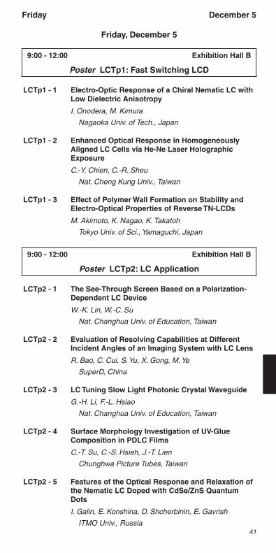
Friday, December 5
9:00 - 12:00 Exhibition Hall B
Poster LCTp1: Fast Switching LCD
LCTp1 - 1 Electro-Optic Response of a Chiral Nematic LC with Low Dielectric Anisotropy
I. Onodera, M. Kimura
Nagaoka Univ. of Tech., Japan
LCTp1 - 2 Enhanced Optical Response in Homogeneously Aligned LC Cells via He-Ne Laser Holographic Exposure
C.-Y. Chien, C.-R. Sheu
Nat. Cheng Kung Univ., Taiwan
LCTp1 - 3 Effect of Polymer Wall Formation on Stability and Electro-Optical Properties of Reverse TN-LCDs
M. Akimoto, K. Nagao, K. Takatoh
Tokyo Univ. of Sci., Yamaguchi, Japan
9:00 - 12:00 Exhibition Hall B
Poster LCTp2: LC Application
LCTp2 - 1 The See-Through Screen Based on a Polarization-Dependent LC Device
W.-K. Lin, W.-C. Su
Nat. Changhua Univ. of Education, Taiwan
LCTp2 - 2 Evaluation of Resolving Capabilities at Different Incident Angles of an Imaging System with LC Lens
R. Bao, C. Cui, S. Yu, X. Gong, M. Ye
SuperD, China
LCTp2 - 3 LC Tuning Slow Light Photonic Crystal Waveguide
G.-H. Li, F.-L. Hsiao
Nat. Changhua Univ. of Education, Taiwan
LCTp2 - 4 Surface Morphology Investigation of UV-Glue Composition in PDLC Films
C.-T. Su, C.-S. Hsieh, J.-T. Lien
Chunghwa Picture Tubes, Taiwan
LCTp2 - 5 Features of the Optical Response and Relaxation of the Nematic LC Doped with CdSe/ZnS Quantum Dots
I. Galin, E. Konshina, D. Shcherbinin, E. Gavrish
ITMO Univ., Russia
Friday December 5
41

LCTp2 - 6 A New Low-Power and High Aperture Ratio for High-Resolution Mobile TN Panels
W. Q. Song, D. L. Fu, J. F. Wu, Y. C. Chang
InfoVision Optoelect., China
LCTp2 - 7 Study on Improving the Image Quality Using Single Compensation Film
B. Hai, C.-T. Kang
Shenzhen China Star Optoelect. Tech., China
9:00 - 12:00 Exhibition Hall B
Poster LCTp3: Photo Alignment
LCTp3 - 1 Multi-Domain IPS LC Cell Using the Photo Alignment Method
B.-J. Mun, K.-W. Park, G.-D. Lee
Dong-A Univ., Korea
LCTp3 - 2 Localized Cell Parameter Comparison of Photo Alignment and Rubbing Type in FFS-LCD
K.-T. Huang, Y.-W. Hung, R.-X. Fang, Y.-T. Chao, T. Lee, C. Lee
HannStar Display, Taiwan
LCTp3 - 3 Fast Switchable Ferroelectric LC Grating and Analysis for the Parameters
Y. Ma, L. Shi, A. K. Srivastava, V. G. Chigrinov, H. S. Kwok
Hong Kong Univ. of S&T, Hong Kong
9:00 - 12:00 Exhibition Hall B
Poster LCTp4: LC Materials
LCTp4 - 1 Modeling of LC/Dendrimer Mixtures by Using Hard Repulsive Molecules
T. Koda, M. Uchida, A. Nishioka, O. Haba, K. Yonetake, M. Kwak*, Y. Momoi*, N. Kim*, S. Hong*, D. Kang*, Y. Choi*
Yamagata Univ., Japan *LG Display, Korea
LCTp4 - 2 Single Hydrogen-Bonded Discotic Complexes: A Simple and Robust Route to Room Temperature Columnar Mesophases
I.-T. Sohn, B.-S. Lee, Y. J. Byun, J. H. Lee
Myongji Univ., Korea
Friday December 5
42

LCTp4 - 3 Pretilt Angle Control of LC on Doping Silica Nanoparticles and Reactive Monomers
C.-J. Hsu, C.-C. Kuo, C.-D. Hsieh, C.-Y. Huang
Nat. Changhua Univ. of Education, Taiwan
9:00 - 12:00 Exhibition Hall B
Poster LCTp5: LC Evaluation
LCTp5 - 1 Analysis on Flexoelectric Effect in AH-IPS LC Mode under Low Frame Rate Driving Using a High Speed Camera
D.-J. Lee*,**, G.-Y. Shim**, S.-H. Yoo**, J.-H. Lee*, J.-H. Baek*, H. Choi*, H.-R. Kim**
*LG Display, Korea **Kyungpook Nat. Univ., Korea
LCTp5 - 2 Proposal of Measuring the Difference in Flexoelectric Coefficient of a TN-LC Cell by Transmission Ellipsometry
F. B. Z. Arif, H. Matsumoto, M. Kimura, T. Akahane
Nagaoka Univ. of Tech., Japan
LCTp5 - 3 Analysis of the Vertical Crosstalk of Advanced Super Dimension Switch Mode TFT-LCD
S. Wang, J. Li, S. Q. Huang, W. Xue, Y. J. Wang, Y. Shi, Q. Y. Guo, K. H. Park, Y. B. Lee, S. K. Lee
Hefei BOE Optoelect. Tech., China
LCTp5 - 4 Measurement for Sum of Flexoelectric Coefficients for Nematic LCs by Using Capacitance Characteristics under Applying the DC Voltage
S. Nakamura, Y. Kudoh, T. Takahashi
Kogakuin Univ., Japan
Friday December 5
EXHIBITION
12:40 – 18:00 Wednesday, Dec. 3, 2014 10:00 – 18:00 Thursday, Dec. 4, 2014 10:00 – 14:00 Friday, Dec. 5, 2014
Exhibition Hall BTOKI MESSE Niigata Convention Center
Free admission with your registration name tag
43

Workshop on Active Matrix Displays
Wednesday, December 3
14:00 - 17:00 Exhibition Hall B
Poster AMDp1: Oxide TFTSpecial Topics of Interest on Oxide-Semiconductor TFT
AMDp1 - 1 Influence of Subthreshold Leakage Current on Temperature Dependence of Oxide TFTs with Light-Induced Bias-Stress
B.-L. Yeh, C.-N. Lin
AU Optronics, Taiwan
AMDp1 - 2 A 31-in. FHD AMOLED TV Driven by Amorphous IGZO TFTs
H.-J. Zhang, C.-Y. Su, W.-H. Li, L.-Q. Shi, X.-W. Lv, Y.-T. Hu, C.-Y. Tseng, Y.-F. Wang, C.-C. Lo
Shenzhen China Star Optoelect. Tech., China
AMDp1 - 3 5.8-in. Indium Gallium Zinc Oxide TFT LCD with Slim Border
E.-C. Liu, Y.-H. Chen, S.-C. Chiang, Y.-J. Lu, Y.-Y. Huang
Chunghwa Picture Tubes, Taiwan
AMDp1 - 4 Investigation of Hysteresis in Dual-Gate a-IGZO TFTs
Y.-H. Kim, J. G. Um, S. Lee, M. Mativenga, J. Jang
Kyung Hee Univ., Korea
AMDp1 - 5 CVD-Free and Low Temperature a-InGaZnO TFTs for Flexible Display Applications
W.-T. Lin, C.-C. Cheng, C.-Y. Liu, M.-F. Chiang
AU Optronics, Taiwan
AMDp1 - 6 Investigation for the Time-Dependent Characteristics of Sol-Gel Processed Zinc-Tin-Oxide (ZTO) Transistors
Y. W. Wang, T. M. Jian, H. H. Wang, W. L. Liu
Nat. Chang Hua Univ. of Education, Taiwan
AMDp1 - 7 Electrical Characteristics and Stability of Bottom Gate a-InGaZnO TFTs with Different Geometric Structures
H.-W. Li, C.-P. Chang, H.-H. Lu
AU Optronics, Taiwan
Wednesday December 3
44

AMDp1 - 8 Hysteresis Improvements by Introducing a Double-Active-Layered Structure in a-InGaZnO TFTs
Y.-C. Tsai, F.-J. Chan, P.-T. Liu, H.-P. D.-D. Shieh
Nat. Chiao Tung Univ., Taiwan
AMDp1 - 9 Self Heating Induced Hole Trapping at Back-Channel Edge of Flexible a-InGaZnO TFTs under Gate and Drain Bias Stress
G. Li*, B.-R. Yang*,**, Y.-C. Tsai***, R. Zhan*, C.-Y. Su****, C.-Y. Lee****, C.-Y. Tseng****, C.-C. Lo****, A. Lien*****, S. Deng*, N. Xu*, H.-P. D.-D. Shieh***
*Nat. Sun Yat-Sen Univ., China **SYSU-CMU Shunde Int. Joint Res. Inst., China ***Nat. Chiao Tung Univ., Taiwan ****Shenzhen China Star Optoelect. Tech., China *****TCL Corporate Res., China
AMDp1 - 10 Enhancement of Performance and Storage Stability of Thin-Film Transistor with InZnSnO/InGaZnO Bilayer Stack Channel Layers
P.-T. Liu, C.-S. Fuh, C.-H. Chang, C.-C. Chang, X.-Y. Yeh
Nat. Chiao Tung Univ., Taiwan
AMDp1 - 11 Effects of Negative-Gate-Bias with Illumination Stress on the Hysteresis in the Transfer Curve of a-IGZO TFT Measured by the New Sampling Method
Y.-J. Chen, Z.-H. Cai, Y.-H. Tai, C.-Y. Chang, C.-J. Li*, Y.-H. Yeh*
Nat. Chiao Tung Univ., Taiwan *ITRI, Taiwan
AMDp1 - 12 Back-Channel-Etching (BCE) TFT Fabrication with High Etchant-Resistive Solute Metal Oxide Semiconductor
K.-H. Su, M. Marinkovic, D.-V. Pham, A. Merkulov, A. Hoppe, R. Anselmann
Evonik Inds., Germany
AMDp1 - 13 Reduction of Hysteresis in Transfer Characteristics of Solution Processed IZTO TFT by Plasma Treatment
T.-H. Kim, C. Avis, H.-R. Hwang, J. Jang
Kyung Hee Univ., Korea
AMDp1 - 14 Effect of Solution Processed AlOX Passivation on Back Channel Etch a-IGZO TFTs
S. An, M. Mativenga, X. Lee, J. Jang
Kyung Hee Univ., Korea
Wednesday December 3
45

AMDp1 - 15 Impact of Negative Bias and Illumination Stress on Channel and Series Resistance of Back Channel Etched a-IGZO TFTs
M. Chun, J. Um, M. Mativenga, J. Jang
Kyung Hee Univ., Korea
14:00 - 17:00 Exhibition Hall B
Poster AMDp2: Active-Matrix Devices
AMDp2 - 1 Study of TFT-LCD Greenish Phenomenon
W. Qin, H. Kim, J.-Y. Zhao, Y. Wei, C.-F. Zhang, L. Wang, S. Kim, J.-J. Mok
BOE Tech. Group, China
AMDp2 - 2 Driving Circuit of Fast Current Programming and Leakage Current Compensation for External Compensation on AMOLED Panel
C.-C. Chen, K.-Y. Lee, H.-S. Lin, L.-H. Chang, Y.-H. Lin
AU Optronics, Taiwan
AMDp2 - 3 Active Matrix Organic Light Emitting Diode Compensative Circuit with Amorphous Silicon TFTs
G.-T. Zheng, P.-T. Liu*, R.-J. Chen*, C.-Y. Tsai*, H.-H. Hsieh**
Nat. Tsing Hua Univ., Taiwan *Nat. Chiao Tung Univ., Taiwan **Giantplus Tech., Taiwan
AMDp2 - 4 Simple Pixel Circuit Using LTPS TFTs with Mirror Compensation for AMOLED Displays
P.-S. Chen, Y.-T. Liu, F.-H. Chen, C.-L. Lin
Nat. Cheng Kung Univ., Taiwan
AMDp2 - 5 New AMOLED Pixel Circuit to Compensate for VTH Variation with an Eliminated VDD Line
Y.-T. Liu, P.-S. Chen, P.-S. Shieh, C.-L. Lin
Nat. Cheng Kung Univ., Taiwan
AMDp2 - 6 Circuit of Gate Driver on Array with Direct Threshold Voltage Compensation for the Pull-Down Transistors
Z.-H. Cai, Y.-J. Chen, Y.-H. Tai, C.-Y. Chang, C.-L. Wu*, Y.-H. Yeh*
Nat. Chiao Tung Univ., Taiwan *ITRI, Taiwan
Wednesday December 3
46

AMDp2 - 7 Design of High Reliable and Self-Healing Integrated Gate Driving Circuit Applied for Amorphous Silicon TFT-LCDs
C. Dai, T. Lee, T.-C. Lai, C.-C. Lo, A. Lien*
Shenzhen China Star Optoelect. Tech., China *TCL Corporate Res., China
Thursday, December 4
9:00 - 10:15 Snow Hall A
AMD1: High Resolution Displays Using LTPS and Oxide TFTsSpecial Topics of Interest on Oxide-Semiconductor TFT
Chair: T. Kamiya, Tokyo Inst. of Tech., JapanCo-Chair: K. Takatori, NLT Techs., Japan
AMD1 - 1:9:00
Invited High PPI Technologies for Mobile Displays
A. Takimoto
Japan Display, Japan
AMD1 - 2:9:25
Invited Advantages of IGZO Platform in Ultra-High-Resolution LCD Applications
N. Ueda, Y. Ogawa, K. Okada, A. Oda, S. Katoh, S. Uchida, K. Yamamoto, T. Matsuo, H. Kawamori
Sharp, Japan
AMD1 - 3:9:50
Invited Ultra High-Definition OLED Display Using C-Axis Aligned Crystalline Oxide Semiconductor FETs
H. Miyake, S. Kawashima, S. Inoue, M. Shiokawa, A. Suzuki, S. Eguchi, Y. Hirakata, J. Koyama, S. Yamazaki, T. Sato*, T. Shigenobu*, Y. Ohta**, S. Mitsui**, N. Ueda**, T. Matsuo**
Semiconductor Energy Lab., Japan *Advanced Film Device, Japan **Sharp, Japan
----- Break -----
10:45 - 12:20 Snow Hall A
AMD2: Physics of Oxide SemiconductorsSpecial Topics of Interest on Oxide-Semiconductor TFT
Chair: J. Jang, Kyung Hee Univ., KoreaCo-Chair: N. Morosawa, Sony, Japan
AMD2 - 1:10:45
Invited Multiple Origins of Near-VBM Defects and Its Passivation Effects in Amorphous In-Ga-Zn-O
T. Kamiya, H. Kumomi, H. Hosono
Tokyo Inst. of Tech., Japan
Wed./Thu. December 3/4
47

AMD2 - 2:11:10
Invited Thermalization Energy Analysis of the Stability of Amorphous Oxide Thin Film Transistors
A. J. Flewitt
Univ. of Cambridge, UK
AMD2 - 3:11:35
Invited Origin of High Photoconductivity Gain and Persistent Photoconductivity in Nanocrystalline Oxide Photo-Sensors
S. Jeon
Korea Univ., Korea
AMD2 - 412:00
Differences in Crystalline Morphology among Crystalline Oxide Semiconductors
K. Dairiki, Y. Nonaka, M. Koyama, Y. Yamada, A. Shimomura, N. Sorida, E. Takahashi, M. Takahashi, S. Yamazaki
Semiconductor Energy Lab., Japan
----- Lunch -----
13:30 - 14:55 Snow Hall A
AMD3: Stability of Oxide TFTSpecial Topics of Interest on Oxide-Semiconductor TFT
Chair: S. Jeon, Korea Univ., KoreaCo-Chair: M. Kimura, Ryukoku Univ., Japan
AMD3 - 1:13:30
Invited Improved Electrical Characteristics and Stability Using Various Post Treatments on Sputtered In-Ga-Zn-O Thin-Film Transistors
Y. J. Tak, S. P. Park, H. Lee, H. J. Kim
Yonsei Univ., Korea
AMD3 - 213:55
Reliability of Amorphous InGaZnO Thin Film Transistors with Low Water-Absorption Passivation Layer
S. Ishikawa, K. Hamada, C. Kulchaisit*, M. Fujii*, Y. Ishikawa*, Y. Uraoka*
JSR, Japan *Nara Inst. of S&T, Japan
AMD3 - 314:15
Channel Length Dependent Bias and Light Stability of Bulk Accumulation a-IGZO TFTs with Top Gate Offsets
S. Lee, M. Mativenga, J. Jang
Kyung Hee Univ., Korea
Thursday December 4
48

AMD3 - 414:35
Effect of Parasitic Capacitance on Pixel Compensation Circuit Developed by Oxide TFT
C.-Y. Lee, W.-C. Hsu, M.-W. Shih, Y.-L. Chen, C.-C. Huang, L.-W. Liu, C.-K. Lo, H.-G. Chang, L.-F. Lin, C.-H. Liu, L.-H. Chang, Y.-H. Lin
AU Optronics, Taiwan
----- Break -----
15:15 - 16:20 Snow Hall A
AMD4: Higher Performance Oxide TFTSpecial Topics of Interest on Oxide-Semiconductor TFT
Chair: H. J. Kim, Yonsei Univ., KoreaCo-Chair: H. Kumomi, Tokyo Inst. of Tech., Japan
AMD4 - 1:15:15
Invited Bulk Accumulation Oxide TFTs for High Resolution Displays
J. Jang, M. Mativenga, D. Geng
Kyung Hee Univ., Korea
AMD4 - 215:40
High Mobility Zn-Free Oxide Thin Film Transistors
T. Kugimiya, M. Ochi, A. Hino, H. Goto, M. Kanamaru*
Kobe Steel, Japan *Kobelco Res. Inst., Japan
AMD4 - 316:00
Amorphous In2O3-Based Thin Film Transistors Fabricated by Low-Thermal Budget Process with High Mobility and Transparency
C.-H. Chang, C.-S. Fuh, C.-J. Chang, C.-C. Chang, X.-Y. Yeh, P.-T. Liu, H.-H. Lin*, K.-L. Fang*, Y.-C. Kao*, C.-L. Lee*, P.-L. Shih*, W.-C. Chang*, I.-M. Lu*
Nat. Chiao Tung Univ., Taiwan *Yeh Hsin Tech., Taiwan
----- Break -----
17:00 - 18:10 Snow Hall A
AMD5: Printed ElectronicsSpecial Topics of Interest on Printed Electronics
Chair: Y. Fujisaki, NHK, JapanCo-Chair: H. Minemawari, AIST, Japan
AMD5 - 1:17:00
Invited High Performance Polymer Semiconductors
A. Ohno
Mitsubishi Chem., Japan
Thursday December 4
49

AMD5 - 2:17:25
Invited Flexible Printed Organic TFT Array and Integrated Circuits
S. Tokito
Yamagata Univ., Japan
AMD5 - 317:50
Alignment Control of Patterned Organic Semiconductor Crystals in Short Channel Organic Thin-Film Transistors
Y. Fujisaki, D. Takahashi*, Y. Nakajima, H. Tsuji, M. Nakata, T. Yamamoto
NHK, Japan *Tokyo Univ. of Sci., Japan
Author Interviews and Demonstrations18:30 – 19:30
Supporting Organizations:Technical Committee on Electronic Information Displays, Electronics
Society, IEICEThin Film Materials & Devices Meeting
Thursday December 4
IDW ’15The 22nd International Display Workshops
December 8 – 11, 2015
Otsu Prince HotelOtsu, Japan
http://www.idw.or.jp
IDW Best Paper Award
IDW OutstandingPoster Paper Award
These awards will go to the most outstanding papers selected from those presented at IDW ’14.
The 2014 award winners will be announced on the IDW website: http://www.idw.or.jp/award.html
50

Workshop on FPD Manufacturing, Materials and Components
Wednesday, December 3
14:00 - 15:20 Marine Hall
FMC1: Manufacturing Technologies
Chair: M. Kimura, Nagaoka Univ. of Tech., JapanCo-Chair: P. E. Malinowski, imec, Belgium
FMC1 - 1:14:00
Invited Visualization Analyses of Replication Molding Phenomena in Injection Molding
H. Yokoi
Univ. of Tokyo, Japan
FMC1 - 214:20
Development of Roll to Sheet Gravure Offset-Printed Touch Sensor Fabrication
J. W.-C. Yu, S.-A. Kuo, C.-H. Chen
AU Optronics, Taiwan
FMC1 - 314:40
Patterning of Multicolor OLEDs with Ultra-High Resolution by Photolithography
P. E. Malinowski*, T. Ke*, A. Nakamura**, S. Steudel*, D. Janssen**, Y. Kamochi***, I. Koyama***, Y. Iwai***, P. Heremans*,****
*imec, Belgium **FUJIFILM Elect. Materials (Europe), Belgium ***FUJIFILM, Japan ****Holst Ctr., the Netherlands
FMC1 - 415:00
Ultrafast, All-Laser Precision Manufacturing of Display Cover Glass for Consumer Devices
M. Mielke, D. Gaudiosi, M. Shirk, E. Juban, M. Greenberg, N. Matthew, T. Booth, S. Srinivas
Raydiance, USA
----- Break -----
15:45 - 16:45 Marine Hall
FMC2: Materials and Components
Chair: R. Yamaguchi, Akita Univ., JapanCo-Chair: W. I. Milne, Univ. of Cambridge, UK
FMC2 - 1:15:45
Invited Graphene for Plastic Electronics
W. I. Milne*,**, F. Torissi*, T. Hasan*, M. T. Cole*, M. H. Kang*, A. C. Ferrari*
*Univ. of Cambridge, UK **Tokyo Inst. of Tech., Japan
Wednesday December 3
51

FMC2 - 216:05
A New Type of Alignment Material for Double-Layered Retarders Composed of Polymerizable LC
R. Takasago, A. Tamura, T. Miyahara, S.-I. Morishima, N. Yanagihara, Y. Takahashi, Y. Furuki, S. Yoshida, Y. Ito
FUJIFILM, Japan
FMC2 - 316:25
Inorganic Wave Plates with High Performance in Visible Region Fabricated by Serial Bideposition
N. Koike, K. Sasaki, E. Takahashi, N. Hanashima, A. Takada, M. Suzuki*
Dexerials, Japan *Kyoto Univ., Japan
Author Interviews and Demonstrations17:15 – 18:15
Thursday, December 4
9:00 - 12:00 Exhibition Hall B
Poster FMCp1: Manufacturing Technologies
FMCp1 - 1 High Resolution Technology for FPD Manufacturing
N. Yabu, K. Nagano, N. Izumi
CANON, Japan
FMCp1 - 2 Realization on Short-Pitch with Wing/Body Patterning Technology
Z. Cao, J. Xue, B. Zhang, X. He, S. J. Choi
BOE Tech. Group, China
FMCp1 - 3 Liquid Optical Clear Adhesive Lamination Guideline for Large Size Panels
B. Fu, L. Yan
Henkel, China
FMCp1 - 4 First Ultra Thin Glass Temporary Bonding Technology Apply in LTPS-LCD
C.-H. Liao, C.-H. Chan, S.-P. Chiao, T.-C. Fan, Y.-H. Lai, J.-K. Lu, N. Sugiura
AU Optronics, Taiwan
FMCp1 - 5 Electrostatic Control for Flexible Substrate De-Bonding Process
C.-C. Tsai, H.-P. Shih, C.-C. Wu, C.-W. Kung, K.-W. Lan
ITRI, Taiwan
Wed./Thu. December 3/4
52

FMCp1 - 6 Current Status of Excimer Laser Annealing for High-Volume LTPS Manufacturing
B. A. Turk, R. Paetzel
Coherent, USA
FMCp1 - 7 Direct Morphology Observation of LC-Polymer Boundary Imaged by Atomic Force Microscope
K. Ueda, T. Yamamoto, M. Kimura
Nagaoka Univ. of Tech., Japan
9:00 - 12:00 Exhibition Hall B
Poster FMCp2: Materials and Components
FMCp2 - 1 Analysis of Black Matrix Electric Properties by Thermal Stress
Y. Na, S. Min, M. Kwak, D. Kang, Y. Choi, S. Jeon
LG Display, Korea
FMCp2 - 2 High Thermal Stability Glass Substrate for High Resolution Display
M. Hayashi, T. Murata, Y. Kato, T. Murata, M. Ohji
Nippon Elec. Glass, Japan
FMCp2 - 3 A Study of Spring Impact Hammer to Define the Specification of Impact Test
B.-C. Huang, K.-C. Chang, C.-Y. Chiu, Y.-C. Liu
G-tech Optoelect., Taiwan
FMCp2 - 4 Effect of N2O Doping on the Properties of ZnO Thin Films on a-Al2O3 Using High-Energy H2O Generated by a Catalytic Reaction
Y. Ohashi, S. Kanouchi, N. Yamaguchi, Y. Tamayama, T. Kato, K. Yasui
Nagaoka Univ. of Tech., Japan
FMCp2 - 5 Crystalline Structure and Dislocation Distribution of ZnO Thin Film Grown on A-Plane Sapphire Substrate Using High-Temperature H2O Produced by a Pt-Catalyzed H2 and O2 Reaction
T. Nakamura, Y. Ishiduka, N. Yamaguchi, Y. Tamayama, K. Yasui
Nagaoka Univ. of Tech., Japan
FMCp2 - 6 Development of Novel Primer Material Suitable for Connecting Cyclolefin Polymer Film and ITO Thin Layer
T. Yamate, K. Ono, S. Yamada, H. Suzuki, K. Kumazawa
Nippon Soda, Japan
Thursday December 4
53
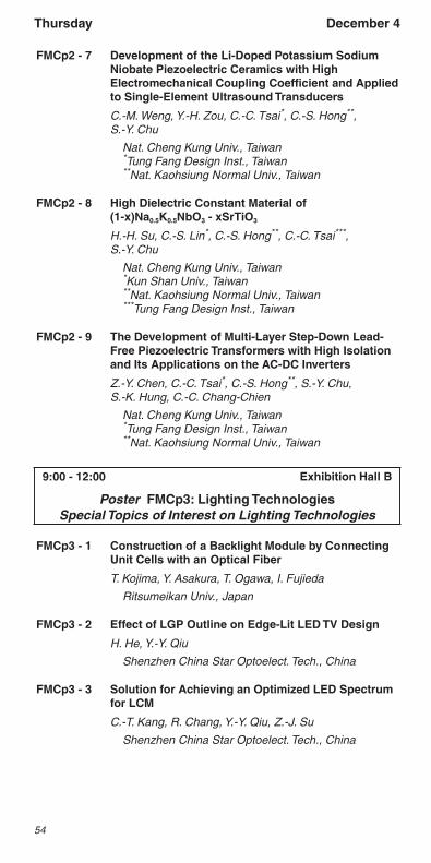
FMCp2 - 7 Development of the Li-Doped Potassium Sodium Niobate Piezoelectric Ceramics with High Electromechanical Coupling Coefficient and Applied to Single-Element Ultrasound Transducers
C.-M. Weng, Y.-H. Zou, C.-C. Tsai*, C.-S. Hong**, S.-Y. Chu
Nat. Cheng Kung Univ., Taiwan *Tung Fang Design Inst., Taiwan **Nat. Kaohsiung Normal Univ., Taiwan
FMCp2 - 8 High Dielectric Constant Material of (1-x)Na0.5K0.5NbO3 - xSrTiO3
H.-H. Su, C.-S. Lin*, C.-S. Hong**, C.-C. Tsai***, S.-Y. Chu
Nat. Cheng Kung Univ., Taiwan *Kun Shan Univ., Taiwan **Nat. Kaohsiung Normal Univ., Taiwan ***Tung Fang Design Inst., Taiwan
FMCp2 - 9 The Development of Multi-Layer Step-Down Lead-Free Piezoelectric Transformers with High Isolation and Its Applications on the AC-DC Inverters
Z.-Y. Chen, C.-C. Tsai*, C.-S. Hong**, S.-Y. Chu, S.-K. Hung, C.-C. Chang-Chien
Nat. Cheng Kung Univ., Taiwan *Tung Fang Design Inst., Taiwan **Nat. Kaohsiung Normal Univ., Taiwan
9:00 - 12:00 Exhibition Hall B
Poster FMCp3: Lighting TechnologiesSpecial Topics of Interest on Lighting Technologies
FMCp3 - 1 Construction of a Backlight Module by Connecting Unit Cells with an Optical Fiber
T. Kojima, Y. Asakura, T. Ogawa, I. Fujieda
Ritsumeikan Univ., Japan
FMCp3 - 2 Effect of LGP Outline on Edge-Lit LED TV Design
H. He, Y.-Y. Qiu
Shenzhen China Star Optoelect. Tech., China
FMCp3 - 3 Solution for Achieving an Optimized LED Spectrum for LCM
C.-T. Kang, R. Chang, Y.-Y. Qiu, Z.-J. Su
Shenzhen China Star Optoelect. Tech., China
Thursday December 4
54

FMCp3 - 4 Portable LED Illuminating Device for Personal Photodynamic Treatment and Cell Culturing
C.-J. Ou, Z.-W. Lin, Y.-S. Lin, P.-Y. Lin, J.-Y. Chen, Y.-K. Tsai
Hsiuping Univ. of S&T, Taiwan
FMCp3 - 5 A Glare Detection for the High-Brightness LED Display Boards Using a Digital Camera
Y.-H. Siao, P.-J. Wu*, B.-J. Pong**, S.-W. Hsu**, C.-H. Wen***, C.-Y. Chen
Nat. Yunlin Univ. of S&T, Taiwan *Nat. Chiao Tung Univ., Taiwan **ITRI, Taiwan ***Nat. Taiwan Univ. of S&T, Taiwan
FMCp3 - 6 The Design of Personal Privacy and Wide Viewing Functions LCM Model Design
Y. W. Chang
AU Optronics, Taiwan
9:00 - 12:00 Exhibition Hall B
Poster FMCp4: Oxide TFT/Printed ElectronicsSpecial Topics of Interest on Oxide-Semiconductor TFT
FMCp4 - 1 Effect of Cu Dopant on Structural and Optical Properties of Zinc Oxide Nanorods
Z. Jin, T. Umakoshi, Y. Abe, M. Kawamura, K. H. Kim
Kitami Inst. of Tech., Japan
FMCp4 - 2 Post-Annealing Effect of Zinc Oxide Nanorods Grown on Al-Doped Zinc Oxide Seed Layers
T. Umakoshi, Y. Abe, M. Kawamura, K. H. Kim
Kitami Inst. of Tech., Japan
FMCp4 - 3 Application of Microwave-Detected Photoconductivity Decay Technique to Process Monitoring in Back Channel Etching-Type TFT Fabrication
H. Goto, M. Ochi, H. Tao, S. Morita, Y. Takanashi, A. Hino, K. Hayashi, T. Kugimiya
Kobe Steel, Japan
FMCp4 - 4 Copper Nano Particle Ink for Reverse Offset Printing and the Application to Thin Film Transistors
M. Koutake*,**
*JAPERA, Japan **DIC, Japan
----- Lunch -----
Thursday December 4
55

17:00 - 18:00 Snow Hall B
FMC3: Optical Films
Chair: H.-M. P. Chen, Nat. Chiao Tung Univ., TaiwanCo-Chair: T. Nonaka, AZ Elect. Materials Manufacturing Japan,
Japan
FMC3 - 1:17:00
Invited Microstructure Film for Wide Viewing TN-LCD
S. Katsuta, E. Yamamoto, Y. Asaoka, T. Kanno, H. Yui, T. Kamada, T. Maeda, Y. Tsuda, K. Kondo
Sharp, Japan
FMC3 - 2:17:20
Invited Meta-Surface Film for Heat-Cutting from the Sun Light
M. Naya, T. Tani, S. Hakuta, H. Yasuda, N. Kiyoto
FUJIFILM, Japan
FMC3 - 317:40
Square Light-Diffusing Film by Collimated UV Light and a Cross Shaped Light Diffuser
B. Katagiri, K. Kusama, T. Orui, S. Shoshi
LINTEC, Japan
Author Interviews and Demonstrations18:30 – 19:30
Friday, December 5
9:00 - 10:00 Snow Hall B
FMC4: Augmented Reality and Virtual RealitySpecial Topics of Interest on Augmented Reality and Virtual Reality
Chair: H. Okumura, Toshiba, JapanCo-Chair: M. Shinohara, Omron, Japan
FMC4 - 1:9:00
Invited Wide Field of View Optical Combiner for Augmented Reality Head-Up Displays
H. Okumura, A. Hotta, T. Sasaki, K. Horiuchi, N. Okada
Toshiba, Japan
FMC4 - 29:20
Panoramic 3D Floating Image Display Using Dual Concave Reflectors
K. Li
Wavien, USA
Thu./Fri. December 4/5
56
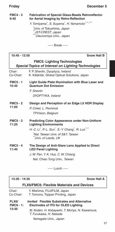
FMC4 - 39:40
Fabrication of Special Glass-Beads Retroreflector for Aerial Imaging by Retro-Reflection
Y. Tomiyama*, S. Suyama*, H. Yamamoto*,**,***
*Univ. of Tokushima, Japan **JST-CREST, Japan ***Utsunomiya Univ., Japan
----- Break -----
10:45 - 12:05 Snow Hall B
FMC5: Lighting TechnologiesSpecial Topics of Interest on Lighting Technologies
Chair: F. P. Shevlin, Dyoptyca, IrelandCo-Chair: K. Käläntär, Global Optical Solutions, Japan
FMC5 - 110:45
Light Guide Plate Illumination with Blue Laser and Quantum Dot Emission
F. Shevlin
DYOPTYKA, Ireland
FMC5 - 211:05
Design and Perception of an Edge Lit HDR Display
P. Cirkel, L. Penninck
TPVision, Belgium
FMC5 - 311:25
Predicting Color Appearance under Non-Uniform Lighting Environments
H.-C. Li*, P.-L. Sun*, S.-Y. Chang*, R. Luo*,**
*Nat. Taiwan Univ. of S&T, Taiwan **Univ. of Leeds, UK
FMC5 - 411:45
The Design of Anti-Glare Lens Applied to Direct LED Panel Lighting
J. W. Pan, Y. K. Hus, C. W. Chiang
Nat. Chiao Tung Univ., Taiwan
----- Lunch -----
13:30 - 14:35 Snow Hall A
FLX6/FMC6: Flexible Materials and Devices
Chair: Y. Mishima, FUJIFILM, JapanCo-Chair: T. Tomono, Toppan Printing, Japan
FLX6/FMC6 - 1:13:30
Invited Flexible Substrates and Alternative Electrodes of ITO for OLED Lighting
M. Koden, H. Kobayashi, T. Moriya, N. Kawamura, T. Furukawa, H. Nakada
Yamagata Univ., Japan
Friday December 5
57

FLX6/FMC6 - 213:55
An Analysis Method of Shock Test for Flexible Displays by Using an Image Luminance Measurement Device
J.-M. Hsu, S.-W. Hsu, B.-J. Wen, T.-Y. Chung
ITRI, Taiwan
FLX6/FMC6 - 314:15
Plastic Substrate Technology for Flexible LCD
Z.-H. Chen, T.-H. Huang, J.-K. Lu, N. Sugiura
AU Optronics, Taiwan
Author Interviews and Demonstrations16:45 – 17:45
Supporting Organizations:Japan Electronics Packaging and Circuits AssociationJapan Society of Colour MaterialRadTech JapanThe Japanese Research Association for Organic Electronics
MaterialsThe Japanese Society of Printing Science and TechnologyThe Society of Photography and Imaging of JapanThe Technical Association of Photopolymers, Japan
Friday December 5
RECEPTIONWednesday, December 3, 2014
19:00 – 21:00Room “Continental” (4F)
Hotel Okura NiigataSee page 12 for details
EXHIBITION
12:40 – 18:00 Wednesday, Dec. 3, 2014 10:00 – 18:00 Thursday, Dec. 4, 2014 10:00 – 14:00 Friday, Dec. 5, 2014
Exhibition Hall BTOKI MESSE Niigata Convention Center
Free admission with your registration name tag
58

Workshop onEL Displays and Phosphors
Thursday, December 4
9:00 - 12:00 Exhibition Hall B
Poster PHp1: Phosphors
PHp1 - 1 Printing Artefacts in the Manufacture of AC Electroluminescence
J. Silver, P. G. Harris
Brunel Univ., UK
PHp1 - 2 PL and EL Characteristics in UV to Blue-Green Emitting Bi-Activated Y2O3-Based Oxide Phosphor Thin Films Prepared by Magnetron Sputtering
T. Miyata, S. Abe
Kanazawa Inst. of Tech., Japan
PHp1 - 3 Local Structural Effect on Emission Characteristics of Organic-Inorganic Hybrid Phosphor Made from Malic Acid and APTES
A. Kato, K. Hasegawa, K. Komatsu, T. Kawase
Nagaoka Univ. of Tech., Japan
PHp1 - 4 Synthesis of Y2WO6:Eu Nano-Rod Phosphor for Local Field Enhanced Inorganic Electroluminescent Devices
A. Kato, S. Matsumoto, D. Imai
Nagaoka Univ. of Tech., Japan
PHp1 - 5 Suppressed Sublimation of Organic Dye Nano-Particles Embedded in Sol-Gel Derived Silica Glass
T. Yamaki, T. Kurabayashi, T. Fukuda, N. Kamata, Z. Honda
Saitama Univ., Japan
9:00 - 12:00 Exhibition Hall B
Poster PHp2: Phosphors for Lighting ApplicationSpecial Topics of Interest on Lighting Technologies
PHp2 - 1 Study on Luminescence Property of Ba3(Sc1-XHox)4O9 Phosphors
K. Sugimoto, S. W. Kim, T. Ishigaki, K. Uematsu, K. Toda, M. Sato
Niigata Univ., Japan
Thursday December 4
59
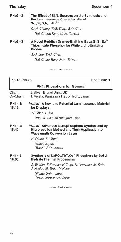
PHp2 - 2 The Effect of Si3N4 Sources on the Synthesis and the Luminescence Characteristic of Sr2-XSi3O2N4: xEu2+
C.-H. Chiang, T.-S. Zhan, S.-Y. Chu
Nat. Cheng Kung Univ., Taiwan
PHp2 - 3 A Novel Reddish Orange-Emitting BaLa2Si2S8:Eu2+ Thiosilicate Phosphor for White Light-Emitting Diodes
S.-P. Lee, T.-M. Chen
Nat. Chiao Tung Univ., Taiwan
----- Lunch -----
15:15 - 16:25 Room 302 B
PH1: Phosphors for General
Chair: J. Silver, Brunel Univ., UKCo-Chair: T. Miyata, Kanazawa Inst. of Tech., Japan
PH1 - 1:15:15
Invited A New and Potential Luminescence Material for Displays
W. Chen, L. Ma
Univ. of Texas at Arlington, USA
PH1 - 2:15:40
Invited Advanced Nanophosphors Synthesized by Microreaction Method and Their Application to Wavelength Conversion Layer
H. Okura, K. Ohmi*
Merck, Japan *Tottori Univ., Japan
PH1 - 316:05
Synthesis of LaPO4:Tb3+,Ce3+ Phosphors by Solid Hydrate Thermal Processing
S. W. Kim, T. Kaneko, K. Toda, K. Uematsu, M. Sato, J. Koide*, M. Toda*, Y. Kudo*
Niigata Univ., Japan *N-Luminescence, Japan
----- Break -----
Thursday December 4
60

17:00 - 18:05 Room 302 B
PH2: Phosphor Applications
Chair: R.-J. Xie, NIMS, JapanCo-Chair: K. Wani, TAZMO, Japan
PH2 - 1:17:00
Invited Development of a UV Light Source Using Pr:LuAG Thin Film Target Pumped by Electron Beam
N. Ichikawa, K. Ikeda, Y. Honda, H. Taketomi, K. Kawai, T. Suzuki
Hamamatsu Photonics, Japan
PH2 - 217:25
Fabrication of Luminescent Thin Film for Nanometric Light Spot of High Spatial Resolution Optical Microscopy
T. Furukawa*, S. Kanamori*, M. Fukuta*, Y. Nawa*, H. Kominami*, Y. Nakanishi*, A. Sugita*, W. Inami*,**, Y. Kawata*,**
*Shizuoka Univ., Japan **JST, Japan
PH2 - 317:45
Growth, Structure, and Cathodoluminescence Property of ZnO Nanorods Prepared with Low Temperature Reducing Annealing
C. Li, X. Li, S. Hou
Kochi Univ. of Tech., Japan
Author Interviews and Demonstrations18:30 – 19:30
Friday, December 5
9:00 - 10:25 Room 302A
PH3: Phosphors for Lighting ApplicationSpecial Topics of Interest on Lighting Technologies
Chair: W. Chen, Univ. of Texas at Arlington, USACo-Chair: K. Ohmi, Tottori Univ., Japan
PH3 - 1:9:00
Invited Quantum Rods Optical Film for Backlight
E. Shaviv, D. Glozman, Y. Bonfil, U. Banin, S. Amir
Qlight Nanotech, Israel
PH3 - 29:25
Thermal Degradation of Green-Emitting SrSi2O2N2:Eu2+
C. Wang, R.-J. Xie*, T. Takeda*, T. Suehiro*, N. Hirosaki*
Univ. of S&T of China, China *NIMS, Japan
Thu./Fri. December 4/5
61

PH3 - 39:45
Wireless Power Transmission Method of a Powder EL Sheet Device
K. Wani, T. Kanda, E. Hashimoto
TAZMO, Japan
PH3 - 410:05
Studies of Electroluminescence from Individual Phosphor Particles
J. Silver, P. G. Harris
Brunel Univ., UK
Author Interviews and Demonstrations16:45 – 17:45
Supporting Organizations:Phosphor Research Society, The Electrochemical Society of JapanThe 125th Research Committee on Mutual Conversion between
Light and Electricity, Japan Society for Promotion of Science
Friday December 5
Evening Get-Together with Wine
Tuesday, December 2, 201418:00 – 20:00
Observation Deck (31F),Hotel Nikko Niigata
(Sponsored by Merck Ltd., Japan)See page 12 for details
IMID 2014August 26 – 29, 2014
EXCO
Daegu, Korea
62

Workshop on Field Emission Displays, CRTs and Plasma Displays
Friday, December 5
9:00 - 9:05 Room 302 B
Opening
Opening Remarks9:00
H. Mimura, Shizuoka Univ., Japan
9:05 - 10:35 Room 302 B
FED1: Novel Devices and Applications
Chair: Y. Gotoh, Kyoto Univ., JapanCo-Chair: F. Wakaya, Osaka Univ., Japan
FED1 - 1:9:05
Invited High Resolution Optical Imaging for Living Cells with Electron Beam Excitation
Y. Kawata*,**, Y. Nawa*, W. Inami*,**
*Shizuoka Univ., Japan **JST-CREST, Japan
FED1 - 29:35
Electrostatic-Focusing Spindt-Type FEA with Improved Electron-Beam Extraction Efficiency for FEA-HARP Image Sensor
Y. Honda*,**, M. Nanba*, K. Miyakawa*, M. Kubota*, M. Nagao***, N. Egami****
*NHK, Japan **Shizuoka Univ., Japan ***AIST, Japan ****Kinki Univ., Japan
FED1 - 39:55
A High-Sensitivity Photodetector Made of Amorphous Selenium and Nitrogen-Doped Diamond Cold Cathode
T. Masuzawa, T. Yamada*, Y. Neo, H. Mimura, D. H. C. Chua**, K. Okano***
Shizuoka Univ., Japan *AIST, Japan **Nat. Univ. of Singapore, Singapore ***Int. Christian Univ., Japan
Friday December 5
63

FED1 - 410:15
Photoassisted Field Emission from P-Type Silicon FEAs
H. Shimawaki, M. Nagao*, T. Yoshida*, Y. Neo**, H. Mimura**, F. Wakaya***, M. Takai***
Hachinohe Inst. of Tech., Japan *AIST, Japan **Shizuoka Univ., Japan ***Osaka Univ., Japan
----- Break -----
10:45 - 12:05 Room 302 B
FED2: Fabrication Processes and New Materials
Chair: H. Mimura, Shizuoka Univ., JapanCo-Chair: H. Shimawaki, Hachinohe Inst. of Tech., Japan
FED2 - 110:45
Fabrication and Emission Characteristics of Ni and Mo Spindt-Type FEAs with Volcano-Structured Focusing Electrode
M. Nagao
AIST, Japan
FED2 - 211:05
Computer Simulation of Electron Beam Trajectories in Double-Gated Spindt-Type FEAs
Y. Gotoh, H. Tsuji, M. Nagao*
Kyoto Univ., Japan *AIST, Japan
FED2 - 311:25
Enhanced Field Emission of CuO Nanowire Arrays by Coating of CNT Network Film
H. Hu, D. Zhang, J. Lin, F. Li, T. Guo
Fuzhou Univ., China
FED2 - 411:45
Electron Emission from MIM Cathodes with an Ag Nanowire Top Electrode
J. Lin, H. Hu, L. Hu, F. Li, T. Guo
Fuzhou Univ., China
----- Lunch -----
Friday December 5
64

13:30 - 14:50 Room 302 B
FED3: FE Mechanisms and PDP Protective Layers
Chair: M. Nagao, AIST, JapanCo-Chair: H. Kajiyama, Tokushima Bunri Univ., Japan
FED3 - 113:30
Observation of Fringelike Emission Pattern in Magnetic Field
Y. Yamada, S. Abo, K. Murakami*, F. Wakaya, M. Abe, M. Takai
Osaka Univ., Japan *Univ. of Tsukuba, Japan
FED3 - 213:50
Work Function Measurements of Tungsten Surface Modified by Praseodymium Oxide by Using Field Emission Microscopy and Retarding Method
T. Kawakubo, K. Kanbara, T. Kitani, H. Nakane*
Nat. Inst. of Tech. Kagawa, Japan *Muroran Inst. of Tech., Japan
FED3 - 314:10
High-Intensity Deep-UV Radiation and Exo-Electron Emission of MgO Powders for AC PDPs
M. Sakai*,**, H. Asano*,**, Y. Fukui*, T. Tsujita*,**, M. Nishitani*,**, H. Kimiya*, R. Murai*, M. Kitagawa**
*Panasonic, Japan **Osaka Univ., Japan
FED3 - 414:30
Electron Storage by Photochromic Transition of Oxide Nanoparticle
H. Kajiyama, T. Matsuura, M. Maekawa*, K. Uchino*, K. Takata**, S. Inoue***
Tokushima Bunri Univ., Japan *Kyushu Univ., Japan **Kansai Univ., Japan ***Hiroshima Univ., Japan
----- Break -----
15:15 - 16:35 Room 302 B
FED4: Summing Up of PDP History
Chair: L. Weber, Consult., USACo-Chair: T. Shiga, Univ. of Electro-Commun., Japan
FED4 - 1:15:15
Invited Summing Up of the PDP History and a Peek at Plasma Technologies Beyond Displays
S. Mikoshiba
Univ. of Electro-Commun., Japan
Friday December 5
65

FED4 - 215:55
A Flexible Luminous Array Film as a Radiation Area Selectable Hg-Free Ultra-Narrow Band UVB Light Source
B. Guo, K. Awamoto, H. Hirakawa, T. Nishimoto*
Plexie, Japan*Yumex, Japan
FED4 - 316:15
Photosynthesis Promotion by Pulsed Light from an AC-PDP Based Fluorescent Film
H. Kajiyama, T. Ohata, I. Kanmai, S. Nagahara, T. Kono, S. Funai, T. Matsuura
Tokushima Bunri Univ., Japan
Author Interviews and Demonstrations16:45 – 17:45
Supporting Organizations:JSPS 158th Committee on Vacuum NanoelectronicsPlasma Display Technical Meeting
Friday December 5
Late-News PapersDue September 25, 2014
Submit a two-page camera-ready manuscriptvia IDW website:
http://www.idw.or.jp/latenews.html
RECEPTIONWednesday, December 3, 2014
19:00 – 21:00Room “Continental” (4F)
Hotel Okura NiigataSee page 12 for details
66

Workshop on OLED Displays and Related Technologies
Wednesday, December 3
14:00 - 15:20 Snow Hall B
OLED1: Advanced OLED Technologies (1)
Chair: T. Wakimoto, Merck, JapanCo-Chair: T. Uchida, Tokyo Polytechnic Univ., Japan
OLED1 - 114:00
Flexibility and Reliability Improvement for Foldable OLED
S.-T. Yeh, G. Chen, C.-H. Tsai, Y.-H. Peng, J.-C. Ho, C.-C. Lee
ITRI, Taiwan
OLED1 - 214:20
An Ultrathin AMOLED Integrated with On-Cell Touch Sensor for Flexible Displays
K.-T. Chen, S.-W. Chen, S.-A. Chen, P.-H. Wang, C.-C. Chang, S.-H. Lee, C.-W. Jung, M.-H. Yeh, K.-J. Chen, J.-Y. Yan, J.-C. Ho, C.-C. Lee
ITRI, Taiwan
OLED1 - 314:40
Black Screen for High Contrast Smart Window AMOLED Display
D. C. Choe, G. W. Kim, R. Lampande, J. H. Kwon
Kyung Hee Univ., Korea
OLED1 - 415:00
High-Transparent 4.65-in. QHD AMOLED Display with 21% Transmittance
C.-T. Lee, Y.-Y. Huang, C.-C. Tsai, C.-C. Kuo, C.-H. Chiu, J.-H. Huang, C.-C. Tsai, Y.-H. Cheng, C.-L. Chen, C.-T. Liang, W.-C. Yen, J.-S. Huang, Y.-W. Chiu, Y.-W. Liu
Chunghwa Picture Tubes, Taiwan
----- Break -----
15:45 - 16:45 Snow Hall B
OLED2: Advanced OLED Technologies (2)
Chair: Y. Kijima, Sony, JapanCo-Chair: S. Naka, Univ. of Toyama, Japan
OLED2 - 115:45
OLED on Silicon for Sensor Applications
M. Thomschke, M. Jahnel, B. Beyer, K. Fehse, U. Vogel
Fraunhofer COMEDD, Germany
Wednesday December 3
67

OLED2 - 216:05
Viewing Angle Spectral Analysis of OLED Display Light Emission Properties
P. M. Boher, T. Leroux, T. Bignon, V. Collomb-Patton
ELDIM, France
OLED2 - 316:25
Natural Stereoscopic Effect Achieved by High-Resolution OLED Display
Y. Yanagisawa, H. Ikeda, M. Jikumaru, D. Kubota, Y. Hirakata, S. Yamazaki, M. Hirose*, M. Kasuga**,***
Semiconductor Energy Lab., Japan *Univ. of Tokyo, Japan **Sakushin Gakuin Univ., Japan ***Utsunomiya Univ., Japan
Author Interviews and Demonstrations17:15 – 18:15
Thursday, December 4
9:00 - 10:10 Snow Hall B
OLED3: OLED Process TechnologiesSpecial Topics of Interest on Printed Electronics
Chair: T. Shimizu, NHK, JapanCo-Chair: T. Komatsu, Panasonic, Japan
OLED3 - 1:9:00
Invited OLED Device Fabrication by Ink-Jet Printing Technology
T. Sonoyama, M. Uchida, T. Sago, S. Watanabe, K. Ishida, M. Ito, M. Ishida, M. Yamada, Y. Okawa, S. Tanabe, H. Kiguchi
Seiko Epson, Japan
OLED3 - 2:9:25
Invited Important Technologies of Ink Jet System for OLED Display Fabrication
T. Hayashi, K. Oshima, S. Takei*, A. Shimamura, Y. Konta, S. Tanabe*
Tokyo Electron, Japan *Seiko Epson, Japan
OLED3 - 39:50
UV-Activated Transparent Desiccant for Practical OLED Encapsulation Process
H. Katsui, T. Miyasako, T. Arai, M. Takahashi, N. Onimaru, N. Takamatsu, T. Yamamura, K. Konno, K. Kuriyama
JSR, Japan
----- Break -----
Wed./Thu. December 3/4
68

10:45 - 11:55 Snow Hall B
OLED4: OLED Materials (1)Special Topics of Interest on Printed Electronics
Chair: K. Nakayama, Yamagata Univ., JapanCo-Chair: K. Monzen, Nissan Chem. Inds., Japan
OLED4 - 1:10:45
Invited Blue Fluorescent OLEDs for Printed Display Applications
E. Boehm, C. Pflumm, H. Heil, S. Meyer, L.-I. Rodriguez, B. Burkhart, F. Eckes, K. Stegmaier, H. Buchholz
Merck KGaA, Germany
OLED4 - 2:11:10
Invited Development and Manufacture of Solution-Processed White OLED Lighting Panel
T. Ogata
Mitsubishi Chem. Group S&T Res. Ctr., Japan
OLED4 - 311:35
The Soluble Hole Injection Materials and the Inks Applicable to OLED Devices
N. Otani, H. Koga, S. Moriyama, T. Endo, N. Nakaie, K. Monzen
Nissan Chem. Inds., Japan
Author Interviews and Demonstrations18:30 – 19:30
13:30 - 16:30 Exhibition Hall B
Poster OLEDp1: OLED Poster Special Topics of Interest on Lighting Technologies
OLEDp1 - 1 Flexible Hybrid White Light Emitting Diodes Based on Small Molecules and Quantum Dots
W. Wu, F. Li, H. Hu, J. Lin, T. Guo
Fuzhou Univ., China
OLEDp1 - 2 Novel Phosphorescent Host Material for Tunable Hybrid White OLED Devices
H.-L. Huang, B. Balaganesan, H.-M. Kuo, B.-W. Xie, T. -C. Chao, M. -R. Tseng
eRay Optoelect. Tech., Taiwan
Thursday December 4
69

13:30 - 16:30 Exhibition Hall B
Poster OLEDp2: OLED PosterSpecial Topics of Interest on Printed Electronics
OLEDp2 - 1 High-Mobility Solution-Processed Organic Field-Effect Transistors with Channel Length of 5 µm
R. Nakamichi, T. Nagase, T. Kobayashi, Y. Sadamitsu*, H. Naito
Osaka Pref. Univ., Japan *Nippon Kayaku, Japan
13:30 - 16:30 Exhibition Hall B
Poster OLEDp3: OLED Poster
OLEDp3 - 1 Polyfluorenes Containing Partially Hydrolyzed Phosphonate Pendant Groups as Electron-Injection Layer for PLEDs
Y. Chen, C.-Y. Chou, H.-A. Lu, C.-P. Chen, Y.-J. Lin, C.-S. Wu
Nat. Cheng Kung Univ., Taiwan
OLEDp3 - 2 Inverted Transparent Organic Light-Emitting Diodes (i-TOLEDs) Comprising Metal Oxide Compounds as Electron-Injection Layer without Alkali Metal
R. Tejima, M. Ichikawa, Y. Hoshi, T. Uchida
Tokyo Polytechnic Univ., Japan
OLEDp3 - 3 The Study of High Resolution Micro-Contact Printing Technology on 4-in. 441 ppi FHD OLED Display
J.-A. Cheng, P.-C. Lin, Q. Li*, Z. Zhu*, D. An*, L.-N. Chien, C.-T. Lin, I.-W. Wu**, I.-M. Lu, S. Fan*
Yeh Hsin Tech. Consulting, Taiwan *Tsinghua Univ., China **Century Tech., China
OLEDp3 - 4 Enhancement of Hole-Injection and Power Efficiency of Organic Light Emitting Devices Using an Ultra-Thin MnO-Doped ZnO Buffer Layer
H.-W. Lu, P.-C. Kao*, S.-Y. Chu
Nat. Cheng Kung Univ., Taiwan *Nat. Chiayi Univ., Taiwan
OLEDp3 - 5 Characterization of Metals/Pentacene Interfaces by Hard X-Ray Photoelectron Spectroscopy
I. Hirosawa, T. Watanabe, H. Oji, K. Tada*, N. Yoshimoto*
JASRI, Japan *Iwate Univ., Japan
Thursday December 4
70

OLEDp3 - 6 Surface-Light-Emitting Transistors Using a P-Type Metal-Base Organic Transistors
N. Kogasaka, H. Muto, K. Nakayama
Yamagata Univ., Japan
OLEDp3 - 7 A Characterization and Evaluation Method for a Gas Barrier Film and Polarizer to Predict Minimum Bending Diameter Allowed in a Flexible OLED Device
A. T. Huang, S.-T. Ho, S.-H. Hung, M.-T. Lee
AU Optronics, Taiwan
OLEDp3 - 8 Analysis of Exciton Quenching Dynamics of Ir(ppy)3 with Hole Measured by Time-Resolved Luminescence Spectroscopy
S. Oyama, H. Sakai, H. Murata
JAIST, Japan
OLEDp3 - 9 Detection of Charged Species in Operating Organic Devices Using Multiple Reflection Absorption Spectra
Y. Akagi, H. Sakai, H. Murata
JAIST, Japan
OLEDp3 - 10 In Situ Characterization of the Charge Transport and Crystal Structural Properties in Organic Thin Film Transistor
T. Watanabe, T. Koganezawa, M. Kikuchi*, K. Nishida*, N. Yoshimoto*, I. Hirosawa
JASRI, Japan *Iwate Univ., Japan
OLEDp3 - 11 Mechanistic Analysis for Preferable Performances at High Temperature of the OLED Device with New Electron Transport Material
K. Nomura, T. Tanaka
TOSOH, Japan
OLEDp3 - 12 High Efficiency Blue Phosphorescent Organic Light-Emitting Diodes with Various Host Materials
S. H. Kim, Y. J. Kim, Y.H.Son, J.M.Lee, B.Y.Kang, C.H.Noh, S.H.Kim*, J.H.Kwon
Kyung Hee Univ., Korea *Samsung Elect., Korea
OLEDp3 - 13 Improvement on Equivalent Circuit Model for OLED with Its Luminance Decay Characteristics
J. Wu, Z. Zou, Y. Tang, Y. Zheng
Southeast Univ., China
Thursday December 4
71

OLEDp3 - 14 Efficient Ionization Method of Atomized Droplet for Fabricating Multilayer Organic Light-Emitting Diode
A. Sato, T. Fukuda, N. Kamata, Z. Honda
Saitama Univ., Japan
OLEDp3 - 15 A Fast Evaluation of Barrier Tapes for In-Plane Water Vapor Permeation in Conventional Ca Film Tests
S.-T. Ho, S.-H. Hung, W.-L. Hung, C.-L. Wang, M.-T. Lee
AU Optronics, Taiwan
OLEDp3 - 16 Blue Phosphorescence Light-Emitting Diode with a New CbzOXD Host
H.-J. Chen, T.-L. Chiu, Y.-H. Hsieh*, M.-K. Leung*, J.-H. Lee*
Yuan Ze Univ., Taiwan *Nat. Taiwan Univ., Taiwan
OLEDp3 - 17 High Efficiency Blue Phosphorescence Light-Emitting Diode with Novel CbzTAZ Host
H.-J. Chen, T.-L. Chiu, P.-S. Wang*, J.-H. Lee*, Y.-H. Hsieh*, M.-K. Leung*
Yuan Ze Univ., Taiwan *Nat. Taiwan Univ., Taiwan
OLEDp3 - 18 Enhancement of Polarization Ratio on Polarized Organic Light Emitting Diodes Using Anisotropic Micro Lens Arrays
D. M. Lee, Y. D. Kim, S. I. Jo, C.-J. Yu, J.-H. Kim
Hanyang Univ., Korea
OLEDp3 - 19 Optical Modeling of V-Shaped Organic Solar Cells in Oblique Incidence of Sunlight
J. Yoon, K. Kang, J. Kim
Kyung Hee Univ., Korea
OLEDp3 - 20 Solution Processed N-P Junction for High Performance Organic Light Emitting Diode
J. Kim, H.-M. Kim, J. Jang
Kyung Hee Univ., Korea
Author Interviews and Demonstrations18:30 – 19:30
Thursday December 4
72

Friday, December 5
9:00 - 10:25 Snow Hall A
OLED5: OLED Materials (2)
Chair: S. Aratani, Hitachi, JapanCo-Chair: T. Ikuta, JNC Petrochem., Japan
OLED5 - 1:9:00
Invited Latest Status of Soluble-OLED Material Development
T. Yamada, Y. Tsubata, D. Fukushima, K. Ohuchi, N. Akino
Sumitomo Chem., Japan
OLED5 - 29:25
Electrical Properties of Solution-Processed Hole Injection Layer Analyzed by Impedance Spectroscopy
T. Endo, Y. Horiuchi, N. Otani, K. Monzen
Nissan Chem. Inds., Japan
OLED5 - 39:45
Design to Electron Injection Complex Using Molecular Energy Calculation for High Performance OLED
J. H. Kong, G. H. Kim, M. J. Park, H. W. Bae, J. H. Kwon
Kyung Hee Univ., Korea
OLED5 - 410:05
Iridium-Free OLED Solutions for the Whole Color Spectrum
M. Mydlak, D. Volz, D. Zink, T. Baumann, H. Flügge, C. Fléchon, J. Navarro
CYNORA, Germany
Author Interviews and Demonstrations16:45 – 17:45
Supporting Organizations:The Japanese Society of Printing Science and TechnologyThe Society of Photography and Imaging of Japan
Friday December 5
IDW ’15The 22nd International Display Workshops
December 8 – 11, 2015
Otsu Prince HotelOtsu, Japan
http://www.idw.or.jp
73

Workshop on 3D/Hyper-Realistic Displays and Systems
Thursday, December 4
9:00 - 12:00 Exhibition Hall B
Poster 3Dp1: 3D/Hyper-Realistic Displays
3Dp1 - 1 Design of Pixel Structure for Color Electronic Holography using One-Dimensional Spatial Light Modulator
A. Ueno, K. Nitta, O. Matoba
Kobe Univ., Japan
3Dp1 - 2 Computer-Generated Hologram using Range Sensors and Digital Cameras at Arbitrary Locations
K. Tai, Y. Sakamoto
Hokkaido Univ., Japan
3Dp1 - 3 Automatic Geometric Calibration in Full-Parallax 3D Display using Holographic Screen
R. Higashida, M. Yamaguchi
Tokyo Inst. of Tech., Japan
3Dp1 - 4 Volumetric 3D Display using Rotating Screens
S. Suzuki, C. Fujikawa, M. Omodani
Tokai Univ., Japan
3Dp1 - 5 Floating Depth-Fused 3D Image using Multi-Focal Lens 3D System for Image Data Reduction
R. Tanimoto*, T. Kurokawa*, H. Yamamoto*,**, S. Suyama*
*Univ. of Tokushima, Japan **Utsunomiya Univ., Japan
3Dp1 - 6 Wide Viewing Zone by Dynamic Head Movement in Edge-Based DFD Display
T. Soumiya, H. Kuribayashi*, H. Yamamoto**, S. Suyama
Univ. of Tokushima, Japan *Nikon, Japan **Utsunomiya Univ., Japan
3Dp1 - 7 Crossed-Mirror Array Converges Sound Wave in 3D Space
R. Kujime, K. Miyamoto, S. Suyama, H. Yamamoto*
Univ. of Tokushima, Japan *Utsunomiya Univ., Japan
Thursday December 4
74

3Dp1 - 8 Perceived Depth Degradation by Delay Time and Discontinuous Image Flipping in Monocular Motion Parallax Display
S. Yamada*, I. Ishii**, H. Yamamoto*,***, S. Suyama*
*Univ. of Tokushima, Japan **Hiroshima Univ., Japan ***Utsunomiya Univ., Japan
3Dp1 - 9 Elimination and Mechanism Study of Binocular Luminance Difference in a 240 Hz Shutter-Type 3D LCDs
Y. Tian, X. Zhang, J. Hsu, C. Chen, C. Dong, X. Lian
Shenzhen China Star Optoelect. Tech., China
3Dp1 - 10 Analysis and Improvement of Color Shift on Angles for 6-in. Stereoscopic Displays with Barriers
H. Wu, H.-J. Yu, D. Xue, Z.-W. Cui, X-Q. Zhao, Z. Hong, Y.-Y. Yin, L. Xin
Beijing BOE Optoelect. Tech., China
3Dp1 - 11 Crosstalk Suppression Based on Gray Couples Measurement
J. Wang, X. Li, Y. Zhang, Z. Xia
Southeast Univ., China
3Dp1 - 12 Study of Imaging Performance Affected by Color Pixel Arrangements and Lenticular Lenses Configuration for Autostereoscopy
Y.-W. Chen, Z.-H. Jhong, C.-R. Sheu
Nat. Cheng Kung Univ., Taiwan
3Dp1 - 13 KANSEI Multimedia Display System That Can Control Smell Discharge Direction and the Psychological Effects
M. Tanaka, R. Shu, R. Shinohara, K. Tomono, A. Tomono
Tokai Univ., Japan
----- Lunch -----
13:30 - 15:00 Room 302 A
3D1: Holography
Chair: H. Yamamoto, Utsunomiya Univ., JapanCo-Chair: M. Tsuchida, NTT, Japan
3D1 - 1:13:30
Invited Real-Time Pupil Tracking for Holographic Display
H.-G. Choo, K. A. Moon, J. Kim
ETRI, Korea
Thursday December 4
75

3D1 - 2:13:55
Invited Color Holographic Display Based on Shifted and Scaled Fractional Fourier Transform
J. Xia, C. Chang, Y. Jiang, W. Lei
Southeast Univ., China
3D1 - 314:20
3D Hologram Reconstruction in the Front of a Transmission Diffuser Screen
J.-F. Chang, W.-C. Su
Nat. Changhua Univ. of Education, Taiwan
3D1 - 414:40
DMD as a Display Device for Holographic Displays
J.-Y. Son, B.-R. Lee*, M.-C. Park**, O. Chernyshov
Konyang Univ., Korea *ETRI, Korea **KIST, Korea
----- Break -----
15:15 - 16:30 Room 301
3D2: Interactive 3D Display TechnologySpecial Topics of Interest on Augmented Reality and Virtual Reality
Chair: M. Tsuchida, NTT, JapanCo-Chair: K. Yamamoto, NICT, Japan
3D2 - 1:15:15
Invited Interactive Display Technologies using High-Speed Image Processing
M. Ishikawa
Univ. of Tokyo, Japan
3D2 - 2:16:00
Invited Floating Digital Signage Based on Aerial Imaging Techniques
H. Yamamoto*,**,***, S. Suyama***
*Utsunomiya Univ., Japan **JST-CREST, Japan ***Univ. of Tokushima, Japan
----- Break -----
17:00 - 18:40 Room 301
3D3: Omnidirectional Hyper-Realistic SystemSpecial Topics of Interest on Augmented Reality and Virtual Reality
Chair: K. Yamamoto, NICT, JapanCo-Chair: M. Tsuchida, NTT, Japan
3D3 - 1:17:00
Invited Characteristic of the Ultra-Realistic Dome Images Estimated from Viewing Behavior
M. Okyudo, C. Yoshizumi
Wakayama Univ., Japan
Thursday December 4
76

3D3 - 2:17:25
Invited Development of Spherical Image Camera RICOH THETA
M. Shohara
Ricoh, Japan
3D3 - 3:17:50
Invited Omnidirectional Video Streaming System with HMD
D. Ochi
NTT, Japan
3D3 - 4:18:15
Invited Holographic HMD with Wide Visual Field
Y. Sakamoto
Hokkaido Univ., Japan
Author Interviews and Demonstrations18:30 – 19:30
Friday, December 5
9:00 - 10:20 Room 301
3D4: 3D/Hyper-Realistic Displays (1)
Chair: H.-G. Choo, ETRI, KoreaCo-Chair: K. Yamamoto, NICT, Japan
3D4 - 19:00
Realization of Homogeneous Brightness for Autostereoscopic Displays with Directional Backlights Composed of Convex Lens Arrays
S. Ishizuka, T. Mukai, H. Kakeya
Univ. of Tsukuba, Japan
3D4 - 29:20
Floating Touch Display Based on a Heterogeneous Imaging System
Y. Maeda, D. Miyazaki, S. Maekawa*
Osaka City Univ., Japan *Parity Innovations, Japan
3D4 - 39:40
A 2D-3D Display with a 120 Hz Hybrid Spatial-Temporal Color LCD
Y. Weng, Y. Zhang, X. Li
Southeast Univ., China
3D4 - 410:00
True Color Optical Simulation of Integral Imaging 3D Display
J. Chen, B. Fang, D. Fan, Q. Liao, Q. Wei, C. Yang, C. Lee, C. Lo, A. Lien*
Shenzhen China Star Optoelect. Tech., China *TCL Corporate Res., China
----- Break -----
Thu./Fri. December 4/5
77

10:45 - 11:45 Room 301
3D5: 3D/Hyper-Realistic Displays (2)
Chair: J.-Y. Son, Konyang Univ., KoreaCo-Chair: M. Tsuchida, NTT, Japan
3D5 - 110:45
3D Image Qualities for the 4K2K TVs
J.-Y. Huang, H.-S. Chen, P.-L. Sun, R. Luo*
Nat. Taiwan Univ. of S&T, Taiwan *Univ. of Leeds, UK
3D5 - 211:05
Examination of Night Driving Support System by the Video Infrared Stereo Night Vision and 3D Television
S. Suidu, T. Endo, M. Yamamoto
Niigata Univ., Japan
3D5 - 311:25
4-D Floating Image Display using Dual Off-Axis Parabolic Reflectors
K. Li
Wavien, USA
----- Lunch -----
13:30 - 14:55 Room 301
3D6: Optical Devices for 3D System
Chair: S. Yano, Shimane Univ., JapanCo-Chair: M. Tsuchida, NTT, Japan
3D6 - 1:13:30
Invited Expanding Depth Directional Stereoscopic Viewing Zone by Continuous Varying Optical Power Lens with Removing Structural Crosstalk in Auto-Stereoscopic 3D
K.-H. Lee
Korea Photonics Tech. Inst., Korea
3D6 - 213:55
A Novel Autostereoscopic Display Designed by Use of Wave Optics Simulation
A. Yuuki, T. Fujino, T. Satake, Y. Niwano, S. Nagano
Mitsubishi Elec., Japan
3D6 - 314:15
Analytical Solutions (Moiré Solver) of the Parameters of 3D Auto-Stereoscopic Multi-View Display.
F. Mukhtarov, S. D. Hwang
Samsung Elect., Korea
Friday December 5
78

3D6 - 414:35
The Design of a Stereo Microscopic Eyepiece by Using a Biprism
S.-W. Yang, T.-H. Lin*, C.-Y. Chen*, K.-L. Huang**, P.-J. Wu***
Nat. Central Univ., Taiwan *Nat. Yunlin Univ. of S&T., Taiwan **Ming Dao Univ., Taiwan ***Nat. Chiao Tung Univ., Taiwan
----- Break -----
15:15 - 16:20 Room 301
3D7/VHF7: Visual Perception for 3D System
Chair: K.-H. Lee, Korea Photonics Tech. Inst., KoreaCo-Chair: Y. Hisatake, Japan Display, Japan
3D7/VHF7 - 1:15:15
Invited Towards the ISO Guideline for Image Safety in Stereoscopic Viewing
T. Bando
AIST, Japan
3D7/VHF7 - 215:40
The Impact of Screen Size on 3D Flicker-Free Luminance
P.-L. Sun*, Y.-P. Hsieh*, H.-S. Chen*, M. R. Luo*,**
*Nat. Taiwan Univ. of S&T, Taiwan **Univ. of Leeds, UK
3D7/VHF7 - 316:00
Measurement of Visual Fatigue Induced by Stereoscopic Display Using an Oddball Based Event-Related Potential Experiment
P. Ye, H. Liang, J. Wang, F. Chen, S. Yang, J. Chen, X. Wu, D. Gao
Nat. Sun Yat-Sen Univ., China
Author Interviews and Demonstrations16:45 – 17:45
Supporting Organizations:Technical Group on Three-Dimensional Image Technology, ITEHolographic Display Artists and Engineers Club, The Japan Society of
Applied Physics
Friday December 5
79

Workshop onApplied Vision and Human Factors
Thursday, December 4
9:00 - 10:10 Room 302 A
VHF1: Optical Measurements
Chair: J. Bergquist, Nokia Techs., JapanCo-Chair: Y. Hisatake, Japan Display, Japan
VHF1 - 1:9:00
Invited General FPD Mura Index under the IEC Measurement Standard
S. Hasegawa, S. Tomioka*, K. Nagamine*
Sony Visual Prods., Japan *Sony, Japan
VHF1 - 29:30
Novel Evaluation Method of Sparkle for LCDs with Different Anti-Glare Films
T.-W. Hsu, Y.-H. Chiang, C.-W. Chen
AU Optronics, Taiwan
VHF1 - 39:50
Spectral Imaging Analysis of OLED Display Light Emission Properties
P. M. Boher, T. Leroux, T. Bignon, V. Collomb-Patton
ELDIM, France
----- Break -----
10:45 - 11:55 Room 302 A
VHF2: Color and OLEDs
Chair: S. Hasegawa, Sony Visual Prods., JapanCo-Chair: K. Masaoka, NHK, Japan
VHF2 - 1:10:45
Invited Visual Effects of Curved AMOLEDs
J. S. Kimmel
Nokia Techs., Finland
VHF2 - 211:15
A Monitor-Based System for Digital Quantification of Deuteranomalous Vision
Y. Tsai, H. Chen, M. R. Luo*
Nat. Taiwan Univ. of S&T, Taiwan *Univ. of Leeds, UK
VHF2 - 311:35
Estimation of the Helmholtz-Kohlrausch Effect in Natural Images Using Gaze Tracking Data
T. Shizume, G. Ohashi, H. Takamatsu*, Y. Shimodaira
Shizuoka Univ., Japan *NEC Display Solutions, Japan
----- Lunch -----
Thursday December 4
80

13:30 - 16:30 Exhibition Hall B
Poster VHFp1: Applied Vision and Human Factors
VHFp1 - 1 Evaluating and Simulating on Luminance Discrepancy between Centre and Fringe of a Liquid Crystal Display
J. Wang, C. Wu, H. Liu, S. Lo
Shenzhen China Star Optoelect. Tech., China
VHFp1 - 2 Object Images Quality Improvement for Transparent Display
Y.-H. Tsai*,**, W.-D. Jeng*, K.-L. Lo**, T.-W. Huang*, O.-Y. Mang*
*Nat. Chiao Tung Univ., Taiwan **ITRI, Taiwan
VHFp1 - 3 Image Qualities of the Curved OLED Displays with Different Picture Setting Modes
J.-Y. Huang, C.-W. Hsu, H.-S. Chen, P.-L. Sun, M. R. Luo*
Nat. Taiwan Univ. of S&T, Taiwan *Univ. of Leeds, UK
VHFp1 - 4 Quantitative Visual Assessment of Moving Image Quality for 4K8K UHDTV Systems
I. Kawahara, H. Sato, H. Tabata
Keisoku Giken, Japan
VHFp1 - 5 Equivalent Spatial Resolution of RxGxBx Subpixel Arrangements
H.-C. Lin, C.-H. Wen, P.-L. Sun, S.-P. Wang*, K.-J. Hu*, M.-C. Lo**
Nat. Taiwan Univ. of S&T, Taiwan *ITRI, Taiwan **Shih Hsin Univ., Taiwan
VHFp1 - 6 Comparison of Accommodation and Convergence among Real Object, 2D Display and 3D Display When a Target Moves along the Depth Direction
S. Mochiduki, Y. Yokoyama, H. Takahira, M. Yamada
Tokai Univ., Japan
VHFp1 - 7 Analysis of Fundamental Characteristics of Movement of Eye and Head When Indexing the Target by the Finger
K. Kikuchi, H. Takahira, R. Ishiro, Y. Tanaka, M. Endou, M. Yamada
Tokai Univ., Japan
Thursday December 4
81

VHFp1 - 8 Analysis of Accommodation and Convergence while Viewing 4K Images
H. Takahira, S. Mochiduki, Y. Yokoyama, M. Yamada
Tokai Univ., Japan
VHFp1 - 9 Analysis of Convergence and Accommodation while Viewing 3D Movies
Y. Shiratori, M. Kitade, H. Takahira, S. Mochiduki, Y. Yokoyama, M. Yamada
Tokai Univ., Japan
VHFp1 - 10 Analysis of Accommodation and Convergence Eye Movement among Medium When a Target Moves along the Depth Direction
Y. Yokoyama, S. Mochiduki, H. Takahira, M. Yamada
Tokai Univ., Japan
----- Break -----
17:00 - 18:00 Room 302 A
VHF3: Moving Image Quality
Chair: T. Kurita, NHK Media Tech., JapanCo-Chair: Y. Nakamura, Mitsubishi Elec., Japan
VHF3 - 117:00
Method of Verifying Accuracy of Pursuit Cameras
M. Rejhon, J. Bergquist*, E. F. Kelley**, P. A. Boynton***
Rejhon Techs., Canada *Nokia Techs., Japan **KELTEK, USA ***NIST, USA
VHF3 - 217:20
A Method of Image Quality Evaluation for Adaptive Temporal Aperture Control with Hold-Type Displays
T. Usui, H. Sato, Y. Takano, T. Yamamoto, K. Ishii
NHK, Japan
VHF3 - 317:40
Image Quality Metrics for Color Breakup Based on Perceived Image Simulation
K. Hirai, N. Torige, T. Horiuchi, S. Tominaga, T. Shibuya*, F. Hasegawa*, M. Nose*
Chiba Univ., Japan *Ricoh, Japan
Author Interviews and Demonstrations18:30 – 19:30
Thursday December 4
82

Friday, December 5
9:00 - 10:00 Room 201
VHF4: Display Legibility
Chair: Y. Shimodaira, Shizuoka Univ., JapanCo-Chair: N. Hiruma, NHK, Japan
VHF4 - 19:00
Model for Flicker Analysis in Reflective LCD in Low Frequency Driving
Y. Kubota, R. Hatsumi, S. Fukai, D. Kubota, Y. Hirakata, S. Yamazaki, M. Hirose*, M. Kasuga**,***
Semiconductor Energy Lab., Japan *Univ. of Tokyo, Japan **Sakushin Gakuin Univ., Japan ***Utsunomiya Univ., Japan
VHF4 - 29:20
Effect of Font Types and Pixel Density of Electronic Displays on the Legibility of Japanese Characters
Y. Hisatake, T. Kawamorita*, Y. Kanno, S. Takahashi**, M. Ito**, H. Takahashi**
Japan Display, Japan *Kitasato Univ., Japan **DNP, Japan
VHF4 - 39:40
Psychological Derivation of Optimal Line Space for Legible Japanese Documents Based on Scheffe’s Method of Paired Comparison
Y. Yonezu, T. Tokui, N. Ishikawa, T. Matsui
Gunma Univ., Japan
----- Break -----
10:45 - 12:15 Room 201
DES3/VHF5: System Design and Evaluation in Augmented RealitySpecial Topics of Interest on Augmented Reality and Virtual Reality
Chair: K. Morita, Nat. Traffic Safety & Environment Lab., JapanCo-Chair: K. Sakamoto, Panasonic, Japan
DES3/VHF5 - 1:10:45
Invited Simulation of Traffic Accident Scenarios with an Augmented Reality Vehicle
N. Uchida, T. Tagawa, K. Sato
Japan Automobile Res. Inst., Japan
DES3/VHF5 - 2:11:10
Invited The Realistic 3D Image Display Using Direct Light Scanning Method
H. Horimai, K. Hattori*, T. Umezaki
3Dragons LLC, Japan *Chubu Univ., Japan
Friday December 5
83

DES3/VHF5 - 311:35
Fast Calculation Algorithm Based on Point-Based Method for CGHs Using Polygon Model
Y. Ogihara, Y. Sakamoto
Hokkaido Univ., Japan
DES3/VHF5 - 411:55
The Superiority of Widespread Monocular Augmented Reality Presentation in a Manual Tracing Task
A. Kitamura, H. Naito, T. Kimura*, K. Shinohara, T. Sasaki**, H. Okumura**
Osaka Univ., Japan *Kansai Univ. of Welfare Scis., Japan **Toshiba, Japan
----- Lunch -----
13:30 - 14:30 Room 302 A
VHF6: Mobile Human Factors and ’Kansei’ Evaluation
Chair: J. S. Kimmel, Nokia Techs., FinlandCo-Chair: T. Nakatsue, Sony, Japan
VHF6 - 113:30
Required Performances of Electronic Displays for Smartphones Revealed by the Survey Results
Y. Hisatake, M. Takemoto*, S. Kubota**
Japan Display, Japan *Seikei Univ., Japan **Ergo Design Lab., Japan
VHF6 - 213:50
An Overall Image Quality Model for Mobile Displays under Different Lighting Conditions
R. Gong*, H. Xu*, M. R. Luo*,**
*Zhejiang Univ., China **Univ. of Leeds, UK
VHF6 - 314:10
Emotion Prediction Model of Museum Lighting
C.-J. Chou, H.-W. Luo, H.-S. Chen, M. R. Luo*
Nat. Taiwan Univ. of S&T, Taiwan *Univ. of Leeds, UK
----- Break -----
Friday December 5
84

15:15 - 16:20 Room 301
3D7/VHF7: Visual Perception for 3D System
Chair: K.-H. Lee, Korea Photonics Tech. Inst., KoreaCo-Chair: Y. Hisatake, Japan Display, Japan
3D7/VHF7 - 1:15:15
Invited Towards the ISO Guideline for Image Safety in Stereoscopic Viewing
T. Bando
AIST, Japan
3D7/VHF7 - 215:40
The Impact of Screen Size on 3D Flicker-Free Luminance
P.-L. Sun*, Y.-P. Hsieh*, H.-S. Chen*, M. R. Luo*,**
*Nat. Taiwan Univ. of S&T, Taiwan **Univ. of Leeds, UK
3D7/VHF7 - 316:00
Measurement of Visual Fatigue Induced by Stereoscopic Display Using an Oddball Based Event-Related Potential Experiment
P. Ye, H. Liang, J. Wang, F. Chen, S. Yang, J. Chen, X. Wu, D. Gao
Nat. Sun Yat-Sen Univ., China
Author Interviews and Demonstrations16:45 – 17:45
Supporting Organizations:Technical Committee on Electronic Information Displays, Electronics
Society, IEICETechnical Group on Information Display, ITE
Friday December 5
RECEPTIONWednesday, December 3, 2014
19:00 – 21:00Room “Continental” (4F)
Hotel Okura NiigataSee page 12 for details
85

Workshop on Projection and Large-Area Displays and Their Components
Wednesday, December 3
14:00 - 14:05 Room 201
Opening
Opening Remarks14:00
S. Ouchi, Hitachi, Japan
14:05 - 15:30 Room 201
PRJ1: Solid-State Light Source Technologies for Projector
Chair: P. Hickl, Barco Control Rooms, GermanyCo-Chair: H. Nakano, Barco, Japan
PRJ1 - 1:14:05
Invited SiC Light Emitting Diode and Its Polarization Control Using a Dressed Photon
T. Kawazoe, K. Nishioka, M. Ohtsu
Univ. of Tokyo, Japan
PRJ1 - 214:30
High Power AlGaInP Red Laser Diode for Display Applications
K. Kuramoto, T. Nishida, S. Abe, M. Miyashita, K. Mori, T. Yanagisawa, T. Yagi
Mitsubishi Elec., Japan
PRJ1 - 314:50
A New Technology for Stabilization of Chromaticity in Laser Projectors
Y. Ogi, Y. Seo, S. Ouchi
Hitachi, Japan
PRJ1 - 415:10
Lighting Technology for Automotive Headlamps
T. Masuda, H. Tanaka, Y. Shibata, M. Hayakawa, S. Yamamura
Koito Manufacturing, Japan
----- Break -----
Wednesday December 3
86

15:45 - 17:15 Room 201
PRJ2: Vehicle Display
Chair: J. Thompson, Texas Instrs., USACo-Chair: K. Ohara, Texas Instrs., Japan
PRJ2 - 1:15:45
Invited Projection Technology Will Take Automotive Head-Up Display to the Next Level
C. Kusaka, J. Kimura
Techno Syss. Res., Japan
PRJ2 - 2:16:10
Invited DLP Technology: Enabling the Next Generation of Automotive Head-Up Display Systems
G. Pettitt, J. Thompson, J. Ferri, M. McCormick
Texas Instrs., USA
PRJ2 - 316:35
Intelligent Head-Up-Display for Driver Assistance
S.-W. Cheng, J.-T. Hsu
Automotive Res. & Testing Ctr., Taiwan
PRJ2 - 416:55
Development of Car Display System with Free-Form Screen
S. Okagaki, J. Kondo, H. Sakamoto, S. Nakahara, M. Kuwata, A. Heishi, H. Yoshii, K. Nakamura, K. Kojima, M. Uno
Mitsubishi Elec., Japan
Author Interviews and Demonstrations17:15 – 18:15
Thursday, December 4
9:00 - 10:05 Room 301
PRJ3: Projection Technologies
Chair: D. Cuypers, imec, BelgiumCo-Chair: H. Kikuchi, NHK, Japan
PRJ3 - 1:9:00
Invited Speckle Reduction by Current-Induced Magneto-Optical Effect Using P-type ZnO Device
N. Tate, T. Kawazoe, M. Ohtsu
Univ. of Tokyo, Japan
PRJ3 - 29:25
Speckle Measurement of Laser Display by Means of Simulating to Human Eye Perception
T. Fukui, K. Suzuki, S. Kubota
Oxide, Japan
Wed./Thu. December 3/4
87

PRJ3 - 39:45
Speckle Reduction by Optimizing Pulse Width of Drive Current for Red Laser Diodes
T. Nishida*,**, T. Yagi*, H. Murata**, Y. Fujiwara**, M. Takemi*
*Mitsubishi Elec., Japan **Osaka Univ., Japan
----- Break -----
10:45 - 11:50 Room 301
PRJ4: Wearable DisplaySpecial Topics of Interest on Augmented Reality and Virtual Reality
Chair: S. Shikama, Setsunan Univ., JapanCo-Chair: S. Ouchi, Hitachi, Japan
PRJ4 - 1:10:45
Invited Laser Light Field Display Based on a Retinal Scanning Array
M. Ide, K. Yoda, S. Kato
Citizen Holdings, Japan
PRJ4 - 211:10
Compact Optical Engine for Smart Glass
H. Baba, T. Totani, T. Hashizume
Seiko Epson, Japan
PRJ4 - 311:30
Light-Guide Optical Element Utilizing Notch Filters for See-Through Glasses
X. Xiao, X. Lin, X. Tan
Beijing Inst. of Tech., China
----- Lunch -----
13:30 - 14:30 Room 302 B
PRJ5: Projection Applications
Chair: F. Shevlin, DYOPTYKA, IrelandCo-Chair: Y. Asakura, Nittoh Kogaku, Japan
PRJ5 - 113:30
Ultra-Short-Throw 4K Projector with Solid-State Light Source
T. Mochizuki, Y. Sato, J. Nishikawa, R. Miyao, H. Kikuchi
Sony, Japan
PRJ5 - 213:50
Stable Optical Projection Screen for Near Seamless Display Walls
P. Hickl
Barco Control Rooms, Germany
Thursday December 4
88

PRJ5 - 314:10
Inorganic Alignment Layers for Liquid Crystal Grating Devices
D. Cuypers*, H. D. Smet*,**
*imec, Belgium **Ghent Univ., Belgium
14:30 - 14:42 Room 302 B
Short Presentation PRJp: Projection
All authors of poster papers for the PRJp1 session will give a brief, 3-minute oral presentation with no discussion time in advance
Author Interviews and Demonstrations18:30 – 19:30
Friday, December 5
9:00 - 12:00 Exhibition Hall B
Poster PRJp1: Projection
PRJp1 - 1 A Wide Laser Head-Up Display with the Complex Refractive Elements
S.-W. Yang, J.-H. Wu*, I.-K. Hsu, P.-J. Wu**, C.-Y. Chen*
Nat. Central Univ., Taiwan *Nat. Yunlin Univ. of Sci. & Tech., Taiwan **Nat. Chiao Tung Univ., Taiwan
PRJp1 - 2 A Study of Optical Design of Laser Projector
W.-T. Li, K.-D. Huang
Nat. Kaohsiung First Univ. of S&T, Taiwan
PRJp1 - 3 Development of Column-Parallel LED Screen with Flexible Shape
K. Sato*, A. Tsuji*, S. Suyama*, H. Yamamoto*,**,***
*Univ. of Tokushima, Japan **JST-CREST, Japan ***Utsunomiya Univ., Japan
PRJp1 - 4 Image Dispersion Compensation Based on Spatial-Multiplexed Holographic Optical Elements
H.-T. Lin, H.-S. Syu, W.-C. Su
Nat. Changhua Univ. of Education, Taiwan
Supporting Organizations:Laser Display Technology Research Group, Optical Society of JapanTechnical Group on Information Display, ITE
Thu./Fri. December 4/5
89

Workshop on Electronic Paper
Wednesday, December 3
14:00 - 14:50 Room 302 A
EP1: Electrophoretic Displays
Chair: G. Zhou, South China Normal Univ., ChinaCo-Chair: M. Tsuchiya, Innova Dynamics, Japan
EP1 - 1:14:00
Invited Three Particle Microencapsulated Electrophoretic Display
M. Wang, C. Lin, P. Laxton, H. Du, H. Zang, M. McCreary*
E-Ink California, USA *E-Ink, USA
EP1 - 2:14:25
Invited Biprimary Dual-Particle Electrokinetic Displays with 70% Reflectance and Greatly Improved Color Saturation
S. Mukherjee, J. Heikenfeld, N. Smith*, M. Goulding*, C. Topping*, S. Norman*, L. Kramer**, Q. Liu**
Univ. of Cincinnati, USA *Merck Chems., UK **Hewlett Packard Res. Lab., USA
----- Break -----
15:45 - 17:00 Room 302 A
EP2: Various Technologies for e-Paper
Chair: M. Omodani, Tokai Univ., JapanCo-Chair: N.-S. Roh, Samsung Display, Korea
EP2 - 1:15:45
Invited Review of Paper-Like Display Technologies
G. Zhou
South China Normal Univ., China
EP2 - 2:16:10
Invited The Progress of Electrowetting Display and Its Applications
L.-C. Chen, W.-Y. Cheng, K.-L. Lo, R.-L. Chang
ITRI, Taiwan
EP2 - 3:16:35
Invited Frontlighting Technologies for Reflective Displays: e-Papers, MEMS, MEOMS, LCDs
K. Käläntär
Global Optical Solutions, Japan
Author Interviews and Demonstrations17:15 – 18:15
Wednesday December 3
90

Thursday, December 4
9:00 - 10:05 Marine Hall
EP3: Chromic Displays
Chair: N. Kobayashi, Chiba Univ., JapanCo-Chair: M. Higuchi, NIMS, Japan
EP3 - 1:9:00
Invited Thermo-Switchable Imaging Media with Dual Emissive and Reflective Modes
K. Nakamura, K. Ogasawara, Y. Kobayashi, K. Kanazawa, N. Kobayashi
Chiba Univ., Japan
EP3 - 29:25
Improvement of Coloration Properties of Electrochromic Cell by Immobilizing Organic Electrochromic Molecules on the Electrode
N. Ura, K. Nakamura, N. Kobayashi
Chiba Univ., Japan
EP3 - 39:45
Design and Preparation of Metallo-Supramolecular Polymers with Improved Electrochromic Properties
M. Higuchi*,**
*NIMS, Japan **JST-CREST, Japan
10:05 - 10:11 Marine Hall
Short Presentation EPp: Electronic Paper
All authors of poster papers for the EPp session will give a brief, 3-minute oral presentation of with no discussion time in advance.
----- Lunch -----
Author Interviews and Demonstrations18:30 – 19:30
13:30 - 16:30 Exhibition Hall B
Poster EPp1: Electronic Paper
EPp1 - 113:30
Improvement of Response of an Electrophoretic Display by Controlling Liquid Flow
K. Sato, M. Omodani
Tokai Univ., Japan
EPp1 - 2 Development of Twisting Balls for e-Paper by a Microchannel Device
H. Akita, Y. Awatsu, Y. Takizawa
Soken Chem. & Eng., Japan
Thursday December 4
91

Workshop on MEMS and Emerging Technologies for Future Displays and Devices
Thursday, December 4
9:00 - 9:10 Room 201
Opening
Opening Remarks: 10th Anniversary Opening Remarks9:00
M. Nakamoto, Shizuoka Univ., Japan
9:10 - 10:30 Room 201
MEET1: Emerging Quantum Dots and Nanotechnologies
Chair: W. Milne, Univ. of Cambridge, UKCo-Chair: Y. Bonnassieux, Ecole Polytechnique, France
MEET1 - 1:9:10
Invited Images and Cathodoluminescent Spectra of Red and Green Quantum Dots
J. Silver, G. R. Fern, T. G. Ireland, S. Coe-Sullivan*, J. S. Steckel*
Brunel Univ., UK *QD Vision, USA
MEET1 - 2:9:30
Invited Progress in Quantum Dots for Liquid Crystal Displays
S. Coe-Sullivan
QD Vision, USA
MEET1 - 3:9:50
Invited Red Quantum Rods under the Electron Microscope
G. R. Fern, S. Jack, F. Schröder-Oeynhausen, T. Jochum*
Brunel Univ., UK *CAN, Germany
MEET1 - 4:10:10
Invited Advancements in On-Chip Quantum Dots for LED Backlights in Wide Color Gamut LCD Displays
J. Osinski, J. Kurtin, N. Puetz, B. Theobold, S. Nathan, B. Mangum
Pacific Light Techs., USA
----- Break -----
Thursday December 4
92

10:45 - 12:45 Room 201
MEET2: Fundamental Components and Process Technologies
Chair: D. Pribat, Sungkyukwan Univ., KoreaCo-Chair: F. Templier, CEA-LETI, France
MEET2 - 1:10:45
Invited CNTs and Graphene for X-ray Systems and Other Applications
W. I. Milne*,**, R. J. Parmee*,**, J. Cameron**, C. Li***, W. Lei***, B. Wang***, M. T. Cole*,**
*Univ. of Cambridge, UK **Cambridge X-ray Syss., UK ***Southeast Univ., China
MEET2 - 2:11:05
Invited Fabrication of Lighting Lamp with Carbon Nanotube Emitters Beam (C-beam)
K. C. Park
Kyung Hee Univ., Korea
MEET2 - 311:25
Sub-Micron Transparent Metal Mesh Conductor for Touch Screen Displays
B. Kobrin, I. McMackin, J. Geddes, O. Seitz, M. Aryal, J. Wassei
Rolith, USA
MEET2 - 4:11:45
Invited Gaussian Density-of-States Model for Organic Devices
Y. Bonnassieux, S. Jung, C. H. Kim, G. Horowitz
Ecole Polytechnique, France
MEET2 - 512:05
Crystallization Technique with Carbon Nanotube Electron Beam (C-beam) Exposure Technique
H. T. Park, J. S. Kang, J. H. Hong, H. Lee, W. J. Kim, K. C. Park
Kyung Hee Univ., Korea
MEET2 - 612:25
Cathodoluminescence Properties of Silicon Thin Films with Carbon Nanotube Electron Beam (C-beam) Exposure Technique
W. J. Kim, J. S. Kang, H. R. Lee, J. H. Hong, H. T. Park, K. C. Park
Kyung Hee Univ., Korea
----- Lunch -----
Thursday December 4
93

13:30 - 14:50 Room 201
MEET3: EL Quantum Dots Technologies
Chair: S. Coe-Sullivan, QD Vision, USACo-Chair: J. Silver, Brunel Univ., UK
MEET3 - 1:13:30
Invited All Solution Processed QLED
J. Jang, J. E. Lee
Kyung Hee Univ., Korea
MEET3 - 2:13:50
Invited Efficient Quantum Dot Light-Emitting Diodes by Improving Charge Carrier Balance
M. Park, H. Jung, J. Lim*, W. Bae**, J. Kwak***, K. Char, S. Lee, C. Lee
Seoul Nat. Univ., Korea *Los Alamos Nat. Lab., USA **KIST, Korea ***Dong-A Univ., Korea
MEET3 - 3:14:10
Invited Quantum Dot Light-Emitting Diodes for Efficient, Solution-Processed Flat Panel Displays
J. R. Manders*, Y. Zheng*, L. Qian*, Y. Yang*, A. Titov*, J. Hyvonen*, J. Tokarz-Scott*, W. Cao**, J. Xue**, C. Morton*, P. H. Holloway*,**
*NanoPhotonica, USA **Univ. of Florida, USA
MEET3 - 414:30
Enhanced Efficiency of Quantum Dot Light-Emitting Diodes by Modifying Sol-Gel Based Metal-Doped ZnO Electron Transport Layer
H. Jung, M. Thambidurai, J. Lim, K. Char, S. Lee, C. Lee
Seoul Nat. Univ., Korea
----- Break -----
15:15 - 16:55 Room 201
MEET4: Novel Materials and Components
Chair: K. C. Park, Kyung Hee Univ., KoreaCo-Chair: G. R. Fern, Brunel Univ., UK
MEET4 - 1:15:15
Invited Graphene-Silicon Composites for Improved Solar Cells
E. Moyen, J. Jo, D. Pribat
Sungkyunkwan Univ., Korea
MEET4 - 215:35
Conducting Graphene Thin Film on Glass with Electron Beam Irradiation
G. C. Lim, J. S. Kang, J. S. Ahn, K. C. Park
Kyung Hee Univ., Korea
Thursday December 4
94

MEET4 - 3:15:55
Invited High Target Utilization Sputtering of Thin Film Metal Oxides for Large-Area Electronics
A. J. Flewitt
Univ. of Cambridge, UK
MEET4 - 416:15
Super Smart Window–Its Energy Design and Some Early Research
H. Morita, H. Yoshida
Tokyo Univ. of Sci., Yamaguchi, Japan
MEET4 - 516:35
Resonator-Type Infrared Detector Released by Plasmaless Sacrificial Si Etching
J.-H. Jeong, S. Kumagai, S. Tajima*, T. Hayashi*, K. Yamakawa**, M. Sasaki
Toyota Tech. Inst., Japan *Nagoya Univ., Japan **Katagiri Eng., Japan
----- Break -----
17:00 - 18:40 Room 201
MEET5: Nanotechnology Display and Imaging
Chair: J. Jang, Kyung Hee Univ., KoreaCo-Chair: A. J. Flewitt, Univ. of Cambridge, UK
MEET5 - 1:17:00
Invited High-Brightness GaN LED Arrays Hybridized on Silicon Interconnect at a Pixel-Pitch of 10 µm.
F. Templier, H. Bono, J.-M. Bethoux, F. Marion, I.-C. Robin, M.-A. di Forte-Poisson*
CEA-LETI, France *3-5 Lab, France
MEET5 - 2:17:20
Invited Mechanical Strengthening of Silicon Torsion Bar of Scanning Micro Mirror by Hydrogen Anneal
S. Yoshida, S. Tanaka, M. Esashi
Tohoku Univ., Japan
MEET5 - 3:17:40
Invited Formation of Conductive AlN by a New Spontaneous Via Holes Technique and Development of Vertical Deep Ultra-Violet Light Emitting Device (RefV-LED)
N. Kurose, Y. Aoyagi
Ritsumeikan Univ., Japan
Thursday December 4
95

MEET5 - 4:18:00
Invited High Brightness Microdisplays by Monolithic Integration of III-V LEDs and Thin Film Silicon Transistors
V. W. Lee
Lumiode, USA
MEET5 - 5:18:20
Invited Quantum Photonic Imager (QPI): A New Display Technology and Its Applications
H. S. El-Ghoroury, Z. Y. Alpaslan
Ostendo Techs., USA
Author Interviews and Demonstrations18:30 – 19:30
Thursday December 4
EXHIBITION
12:40 – 18:00 Wednesday, Dec. 3, 2014 10:00 – 18:00 Thursday, Dec. 4, 2014 10:00 – 14:00 Friday, Dec. 5, 2014
Exhibition Hall BTOKI MESSE Niigata Convention Center
Free admission with your registration name tag
IDW ’14 Tutorial in JapaneseOrganized by SID Japan Chapter
Tuesday, December 2, 2014Room 301, 3F
TOKI MESSE Niigata Convention Center
Detailed information is available onhttp://www.sid-japan.org
Final ProgramThe final program of IDW ’14 will be available on
the website (http://www.idw.or.jp/) from the middle of November.
96

Workshop onDisplay Electronic Systems
Thursday, December 4
9:00 - 10:35 Room 302 B
DES1: Display Technologies in Augmented RealitySpecial Topics of Interest on Augmented Reality and Virtual Reality
Chair: K. Kiyokawa, Osaka Univ., JapanCo-Chair: K. Makita, AIST, Japan
DES1 - 1:9:00
Invited Diminished Reality Based on Image Inpainting for Visually Removing Real Objects in Real Time
N. Kawai
Nara Inst. of S&T, Japan
DES1 - 2:9:25
Invited HMD Technologies for AR
K. Kiyokawa
Osaka Univ., Japan
DES1 - 3:9:50
Invited Fog Display as a Co-creative Expression Media
Y. Miwa, S. Itai, Y. Terada
Waseda Univ., Japan
DES1 - 410:15
Security Doors
H.-F. Wang, C.-C. Lan, J.-Y. Huang, T.-H. Lin, H.-S. Chen
Nat. Taiwan Univ. of S&T, Taiwan
----- Break -----
10:45 - 11:55 Room 302 B
DES2: Image Processing
Chair: A. Ninan, Dolby Labs., USACo-Chair: A. Sakaigawa, Japan Display, Japan
DES2 - 1:10:45
Invited Evolution of Displays through Advances in Next Generation Video
A. Ninan
Dolby Labs., USA
DES2 - 2:11:10
Invited Pursuit of Visually Lossless Compression and Practical Tradeoffs in Display Systems
D. F. Stolitzka
Samsung Display, USA
Thursday December 4
97

DES2 - 311:35
Study of Low Color Shift Design with a WRGB LCD Panel
L.-X. Chen, C.-T. Kang
Shenzhen China Star Optoelect. Tech., China
----- Lunch -----
Author Interviews and Demonstrations18:30 – 19:30
13:30 - 16:30 Exhibition Hall B
Poster DESp1: Display Electronic Systems
DESp1 - 1 Design of Human Face Recognition Application on Wide Viewing Angle Near-Eye See-Through Display
Z. Song, Z. Hu, L. Wang, Y. Tang
Southeast Univ., China
DESp1 - 2 A Study of Optical Design of Automotive Head-Up Display
Y.-C. Fang, B.-R. Hsueh*, Y.-H. Chang
Nat. Kaohsiung First Univ. of S&T, Taiwan *Kao Yuan Univ. of S&T, Taiwan
DESp1 - 3 Amorphous Silicon Integrated Gate Driver Circuits for High Resolution and Narrow Bezel Panel Application
G.-T. Zheng, P.-T. Liu*, C.-H. Chang*, S.-H. Hung*, W.-C. Wang**, Y.-H. Chang**, W.-C. Wang**, W.-L. Sung**
Nat. Tsing Hua Univ., Taiwan *Nat. Chiao Tung Univ., Taiwan **Chunghwa Picture Tubes, Taiwan
DESp1 - 4 Proposal of a Negative Level Shifter for a Negative High Voltage Generator
M. Fukuhara, A. Ueda, M. Urakami, S. Hayakawa, M. Yoshida
Tokai Univ., Japan
DESp1 - 5 A Novel Charge Sharing Method for Liquid Crystal Displays with Lower Power Consumption
Y. Mu*,**, X. Guo*, X. Tang**
*Shanghai Jiao Tong Univ., China **Infovision Optoelect., China
Thursday December 4
98

DESp1 - 6 Introduction of a Liquid Crystal Driving Circuit
X. Xu, Z. Song, J. Chang, C. Gang, A. Jian, R. Lung, X. Chen, B. Liao
Shenzhen China Star Optoelect. Tech., China
DESp1 - 7 Reducing Influence of Bias Stress on AMOLED Displays by Driving in Linear Regime: a Sensitivity Perspective
F. D. Roose*,**, K. Myny**, J. Genoe*,**, P. Heremans*,**, W. Dehaene*
*KULeuven, Belgium **imec, Belgium
DESp1 - 8 External TFT Compensating System for AMOLED Displays
W.-C. Chiou, C.-C. Tsou, P.-S. Chen, C.-L. Lin
Nat. Cheng Kung Univ., Taiwan
DESp1 - 9 A Differential Signal Impedance Matching Solution
Y. Mu*,**, X. Guo*, X. Tang*,**
*Shanghai Jiao Tong Univ., China **Infovision Optoelect., China
DESp1 - 10 Super-Resolution Based on Edge Detection and Sub-Regional Interpolation
H.-L. Hu, H. Li, L.-W. Chu, C. Li, C.-C. Lo
Shenzhen China Star Optoelect. Tech., China
Author Interviews and Demonstrations18:30 – 19:30
Friday, December 5
10:45 - 12:15 Room 201
DES3/VHF5: System Design and Evaluation in Augmented RealitySpecial Topics of Interest on Augmented Reality and Virtual Reality
Chair: K. Morita, Nat. Traffic Safety & Environment Lab., JapanCo-Chair: K. Sakamoto, Panasonic, Japan
DES3/VHF5 - 1:10:45
Invited Simulation of Traffic Accident Scenarios with an Augmented Reality Vehicle
N. Uchida, T. Tagawa, K. Sato
Japan Automobile Res. Inst., Japan
DES3/VHF5 - 2:11:10
Invited The Realistic 3D Image Display Using Direct Light Scanning Method
H. Horimai, K. Hattori*, T. Umezaki
3Dragons, Japan *Chubu Univ., Japan
Thu./Fri. December 4/5
99

DES3/VHF5 - 311:35
Fast Calculation Algorithm Based on Point-Based Method for CGHs Using Polygon Model
Y. Ogihara, Y. Sakamoto
Hokkaido Univ., Japan
DES3/VHF5 - 411:55
The Superiority of Widespread Monocular Augmented Reality Presentation in a Manual Tracing Task
A. Kitamura, H. Naito, T. Kimura*, K. Shinohara, T. Sasaki**, H. Okumura**
Osaka Univ., Japan *Kansai Univ. of Welfare Scis., Japan **Toshiba, Japan
----- Lunch -----
13:30 - 14:30 Room 201
DES4: Display Driving Technologies
Chair: A. Sakaigawa, Japan Display, JapanCo-Chair: T. Yamamoto, NHK, Japan
DES4 - 113:30
Low Power Liquid Crystal Driving Technique Based on Capacitors for 1-Pixel Display
H. Manabe, M. Date*, H. Takada*, H. Inamura
NTT DoCoMo, Japan *NTT, Japan
DES4 - 213:50
Ultra Low Power LCD TV Using RGBW System
C. Jung, Y. Chu, Z. Lai, W. Li, Y. Han, K. Kim, L. Zhang, J. Jun
BOE Tech. Group, China
DES4 - 314:10
Pixel Circuit with Fast Charging Capability Using Charge-Sharing Method for Blue-Phase Liquid Crystal Displays
P.-C. Lai, M.-H. Cheng, P.-C. Lai, C.-L. Lin
Nat. Cheng Kung Univ., Taiwan
----- Break -----
Friday December 5
Final ProgramThe final program of IDW ’14 will be available on
the website (http://www.idw.or.jp/) from the middle of November.
100

15:15 - 16:15 Room 201
DES5: Display Interface and Driving Technologies
Chair: H. Okumura, Toshiba, JapanCo-Chair: T. Yamamoto, NHK, Japan
DES5 - 115:15
An Automatic DC Self-Adjusting Encoder of 5Gbps/Lane Intra-Panel Interface for High Speed Transmission
L.-W. Chang, Y.-C. Wu, Y.-C. Kang, W.-T. Chen, C.-P. Ho, C.-H. Yang
AU Optronics, Taiwan
DES5 - 215:35
A Novel Method to Reduce the Loss of the Data in High Resolution LCD
S.-Y. Wu, Y.-L. Ho, Y.-C. Chen, H.-H. Chen, H.-M. Su, W.-Z. Zeng
Chunghwa Picture Tubes, Taiwan
DES5 - 315:55
A P-Type LTPS TFT Compensation Pixel Circuit for Self-Emission Displays with GOA
Y.-T. Lin, H.-Y. Hsieh, C.-H. Chen, Y.-C. Lai, M.-Y. Lu, C.-C. Kuo, C.-T. Chuang, Y.-S. Huang, C.-N. Yeh, N. Sugiura
AU Optronics, Taiwan
Author Interviews and Demonstrations16:45 – 17:45
Supporting Organizations:Shin-etsu Section, IEEESpecial Interest Group on Mixed Reality, The Virtual Reality Society
of JapanTechnical Committee on Electronic, Information Displays, Electronics
Society IEICETechnical Group on Information Display, ITETechnical Group on Information Sensing Technologies, ITETechnical Committee on Image Engineering, Systems Society, IEICE
Friday December 5
IDW ’14 Tutorial in JapaneseOrganized by SID Japan Chapter
Tuesday, December 2, 2014Room 301, 3F
TOKI MESSE Niigata Convention Center
Detailed information is available onhttp://www.sid-japan.org
101

Workshop on Flexible Electronics
Wednesday, December 3
14:00 - 14:05 Snow Hall A
Opening
Opening Remarks14:00
T. Sekitani, Osaka Univ., Japan
14:05 - 15:40 Snow Hall A
FLX1: Flexible Backplane
Chair: T. Kamata, AIST, JapanCo-Chair: T. Sekitani, Osaka Univ., Japan
FLX1 - 1:14:05
Invited Oxide Thin Film Transistors for Flexible Display
Y. Uraoka, M. Fujii, M. Horita, Y. Ishikawa
Nara Inst. of S&T, Japan
FLX1 - 2:14:30
Invited Improvement in the Field-Effect Mobility of Metal Oxide TFTs by Advanced Stack Channel Structure and Defect Control for the Next-Generation High-End Active-Matrix Displays
J. K. Jeong, A. Y. Hwang, K. Ji, J. H. Song, C. K. Lee, H. Y. Jung
Inha Univ., Korea
FLX1 - 3:14:55
Invited Vertical Organic Field-Effect Transistors for Truly Flexible AMOLED Backplanes
G. Schwartz, H. Kleemann, J. Blochwitz-Nimoth
Novaled, Germany
FLX1 - 415:20
Flexibility Improvement of LTPS-TFT for Foldable AMOLED
J.-Y. Yan, W.-W. Tsai, B.-Y. Su, C.-W. Su, H.-C. Yao, T.-J. Wang, W.-C. Kao, Y.-C. Lin, C.-Y. Hung, W.-H. Chen, M.-J. Yang, C.-Y. Chiang, K.-L. Chuang, W.-T. Wang, C.-C. Lee
ITRI, Taiwan
----- Break -----
Wednesday December 3
102

15:45 - 16:25 Snow Hall A
FLX2: Flexible Displays and Devices
Chair: K. Uemura, Nippon Steel & Sumitomo Metal, JapanCo-Chair: H. Maeda, DNP, Japan
FLX2 - 115:45
Bezel-Less PMOLED Modules with Flexible Substrates for Scalable Display System
H. Iijima, M. Izuchi, H. Makino, T. Wakabayashi, K. Sasai, Y. Okumoto, A. Miyamoto, K. Morita
Panasonic, Japan
FLX2 - 216:05
A Flexible Display Panel, a Flexible Battery, and a Flexible Printed Circuit for Wearable Display
T. Miwa, R. Tajima, Y. Goto, Y. Saito, T. Oguni, H. Miyake, A. Hitotsuyanagi, J. Goto, H. Katagiri, S. Okano, M. Kaneyasu, M. Hiroki, M. Takahashi, S. Yamazaki
Semiconductor Energy Lab., Japan
Author Interviews and Demonstrations17:15 – 18:15
Thursday, December 4
9:00 - 12:00 Exhibition Hall B
Poster FLXp1: Flexible Electronics
FLXp1 - 1 A 4.6-in. Flexible AMOLED Encapsulated by Sputtered Thin Film and Laminated High Barrier Film
L. Lin, C. Zhao, P. Dang, X. Liu, X. Huang, X. Gao
Visionox R&D Ctr., China
FLXp1 - 2 Ultra-High Gas Barrier Film Deposition Using a Novel Precursor, TG-4E, by PECVD for OLED Devices
H. Chiba, M. Shimizu, D. Hara, K. Tokuhisa
TOSOH, Japan
FLXp1 - 3 Flexible Dye Sensitized Solar Cells for Device Power Applications
J. Silver, T. G. Ireland, G. R. Fern, M. Spratt*
Brunel Univ., UK *G24 Power, UK
Wed./Thu. December 3/4
103

FLXp1 - 4 Enhanced Charge Injection of Organic Field-Effect Transistor with 6, 13-Bis(triisopropylsilylethynyl) Pentacene Using a Metal Oxide Buffer Layer
E.-Y. Shin, C.-H. Shin, M.-H. Kim, J.-H. Lee, Y. Choi
Hanbat Nat. Univ., Korea
FLXp1 - 5 The Study on Electrical Characteristics Variation of Flexible Pentacene Based Thin Film Transistors on PET Substrate with/without Surface Treatments
Y. W. Wang, W. L. Liu, J. S. Jiang, T. M. Jian
Nat. Changhua Univ. of Education, Taiwan
FLXp1 - 6 Structure Design of IGZO TFTs with Stress Analysis for Flexible Applications Using Finite Element Method
M. H. Lee, S.-M. Hsu*, C. Liu, J.-D. Shen
Nat. Taiwan Normal Univ., Taiwan *Nat. Taiwan Univ., Taiwan
FLXp1 - 7 Flexible Polymer Dispersed LC Materials for Holographic Recording
K.-T. Kuo, W.-C. Su
Nat. Changhua Univ. of Education, Taiwan
FLXp1 - 8 Study of Polymer Stabilized Blue Phase LC on Flexible Substrate
N. Endo, T. Matsumoto, H. Kikuchi*, M. Kimura
Nagaoka Univ. of Tech., Japan *Kyushu Univ., Japan
FLXp1 - 9 Fabrication of Conductive Electrode on Flexible Substrate Using Ag Nanoparticle Ink by Transfer Printing Method
J.-C. Choi, J.-S. Park, G. T. Park, J.-H. Kim, M.-K. Park, I. Mahmud, J.-H. Bae, H.-R. Kim
Kyungpook Nat. Univ., Korea
FLXp1 - 10 Pretilt Angle and Surface Anchoring Energy of LCD Fabricated by Slit Coater
T. Yamamoto, M. Kimura
Nagaoka Univ. of Tech., Japan
FLXp1 - 11 A Non-Contact Resistance Measurement of Flexible Substrates for Repeating Bending Test by Using a Terahertz Time Domain Spectroscopy
B.-J. Wen, T.-A. Liu, S.-W. Hsu
ITRI, Taiwan
Thursday December 4
104

FLXp1 - 12 The Enhanced Thin Glass with an Ultra-High Bending Strength by a Laser Peeling Technology
C.-H. Li, C.-J. Huang, K.-T. Chen, M.-C. Lin
ITRI, Taiwan
----- Lunch -----
13:30 - 14:45 Snow Hall B
FLX3: Advanced Printing TechnologiesSpecial Topics of Interest on Printed Electronics
Chair: M. Ito, Toppan Printing, JapanCo-Chair: H. Hirata, Toray Eng., Japan
FLX3 - 1:13:30
Invited Novel Roll-to-Roll Screen Printing Machine for Flexible Devices
D. Kobayashi, N. Naoi*, T. Suzuki*, T. Sasaki*, T. Furukawa**
Tokai Shoji, Japan *Tokai Seiki, Japan **Yamagata Univ., Japan
FLX3 - 2:13:55
Invited Technologies for Fully Integrated Printed Displays
N. Fruehauf, M. Strecker, D. Benzel, S. Hoehla, J. Remmele
Univ. of Stuttgart, Germany
FLX3 - 3:14:20
Invited Flexible Transparent Conductive Films Based on Metal Mesh Technology
Z. Cui
Chinese Ac. of Sci., China
----- Break -----
15:15 - 16:25 Snow Hall B
FLX4: Printed TFT TechnologiesSpecial Topics of Interest on Printed Electronics
Chair: Y. Uraoka, Nara Inst. of S&T, JapanCo-Chair: T. Furukawa, Yamagata Univ., Japan
FLX4 - 1:15:15
Invited Fully Printed Flexible TFT Array for Electronic Paper
M. Ito, H. Chujo, K. Murata, M. Nishizawa, N. Ikeda, K. Hatta, M. Yokoo, R. Matsubara, O. Kina, S. Akao, T. Yamamoto, M. Takei, M. Kumagai, M. Ishizaki, K. Morosawa, M. Matsumura
Toppan Printing, Japan
Thursday December 4
105

FLX4 - 2:15:40
Invited Fully-Printed Organic TFTs and Circuits on Ultra-Flexible Substrates
K. Fukuda, Y. Takeda, S. Tokito
Yamagata Univ., Japan
FLX4 - 316:05
Flexible Electronics on Backmolded Plastic Foils
P. Gaucci, N. Fruehauf, A. Ilchmann*, B. Polzinger*, W. Eberhardt*, H. Kueck*
Univ. of Stuttgart, Germany *HSG-IMAT, Germany
Author Interviews and Demonstrations18:30 – 19:30
Friday, December 5
10:45 - 11:50 Snow Hall A
FLX5: Flexible Substrates
Chair: T. Shiro, Teijin, JapanCo-Chair: T. Eguchi, Sumitomo Bakelite, Japan
FLX5 - 1:10:45
Invited Flexible Paper Electronics Based on Cellulose Nanofiber Paper
H. Koga, M. Nogi, K. Suganuma
Osaka Univ., Japan
FLX5 - 211:10
Resent Approach to High Throughput Barrier Coating on Plastic Substrate
T. Okimoto, T. Segawa, H. Tamagaki
Kobe Steel, Japan
FLX5 - 311:30
Development of Transparent Cellulose Nano Fiber Film for Flexible Displays
G. Banzashi, H. Fushimi, S. Iwai, M. Tsunoda, E. Mikami
Oji Holdings, Japan
----- Lunch -----
Thu./Fri. December 4/5
IMID 2014August 26 – 29, 2014
EXCO
Daegu, Korea
106

13:30 - 14:35 Snow Hall A
FLX6/FMC6: Flexible Materials and Devices
Chair: Y. Mishima, FUJIFILM, JapanCo-Chair: T. Tomono, Toppan Printing, Japan
FLX6/FMC6 - 1:13:30
Invited Flexible Substrates and Alternative Electrodes of ITO for OLED Lighting
M. Koden, H. Kobayashi, T. Moriya, N. Kawamura, T. Furukawa, H. Nakada
Yamagata Univ., Japan
FLX6/FMC6 - 213:55
An Analysis Method of Shock Test for Flexible Displays by Using an Image Luminance Measurement Device
J.-M. Hsu, S.-W. Hsu, B.-J. Wen, T.-Y. Chung
ITRI, Taiwan
FLX6/FMC6 - 314:15
Plastic Substrate Technology for Flexible LCD
Z.-H. Chen, T.-H. Huang, J.-K. Lu, N. Sugiura
AU Optronics, Taiwan
Author Interviews and Demonstrations16:45 – 17:45
Supporting Organizations:Technical Committee on Electronic Information Displays, Electronics
Society, IEICETechnical Group on Information Display, ITE
Friday December 5
IDW ’15The 22nd International Display Workshops
December 8 – 11, 2015
Otsu Prince HotelOtsu, Japan
http://www.idw.or.jp
107

Workshop onTouch Panels and Input Technologies
Wednesday, December 3
14:00 - 14:05 Room 302 B
Opening
Opening Remarks14:00
N. Hashimoto, Citizen Holdings, Japan
14:05 - 15:30 Room 302 B
INP1: Touch Panel (1)
Chair: H.-S. Koo, Minghsin Univ. of S&T, TaiwanCo-Chair: K. Nakatani, Touchpanel Labs., Japan
INP1 - 1:14:05
Invited Technological Development of Touch Panel Industry in Taiwan
H.-S. Koo, M. Chen
Minghsin Univ. of S&T, Taiwan
INP1 - 214:30
New Al-Based Metal Mesh Electrode for a Touch Screen Panel
M. Ochi, Y. Shida, H. Goto, T. Kugimiya, K. Moriyoshi*
Kobe Steel, Japan *Kobelco Res. Inst., Japan
INP1 - 314:50
Low Reflectance Metal Layers for New Touch Panel Solutions
J. L. Grillmayer, H. C. Ko, M. Bender*, K. Witting*
Appl. Materials, Taiwan *Appl. Materials, Germany
INP1 - 415:10
A Novel Metal Mesh Single Layer Touch Sensor Design to Achieve Preeminent Touch and Visual Performance
R. Fu, J. Qiu, J. Zhang, C. Ye, Y. Lin, C. Lee, C. Luo, A. Lien
Shenzhen China Star Optoelect. Tech., China
----- Break -----
Wednesday December 3
108

15:45 - 17:15 Room 302 B
INP2: Touch Panel (2) and Haptics
Chair: T. Hoshi, Nagoya Inst. of Tech., JapanCo-Chair: H. Haga, NLT Techs., Japan
INP2 - 1:15:45
Invited Electrostatic Tactile Display for Stimulus Localization
H. Haga, K. Yoshinaga, J. Yanase, D. Sugimoto, K. Takatori, H. Asada
NLT Techs., Japan
INP2 - 2:16:10
Invited Noncontact Tactile Display Using Airborne Ultrasound
T. Hoshi
Nagoya Inst. of Tech., Japan
INP2 - 316:35
Touchless Architecture for Small and Medium Size Panel Application
D.-C. Yu, J.-S. Liao, H.-H. Chen, H.-M. Su, W.-T. Tseng
Chunghwa Picture Tubes, Taiwan
INP2 - 416:55
A Novel Embedded Touch Display with Integrated Chip Solution
Y.-C. Li, C.-C. Chang, W.-J. Yang, C.-Y. Hsu, H.-H. Chen, H.-M. Su, W.-T. Tseng
Chunghwa Picture Tubes, Taiwan
Author Interviews and Demonstrations17:15 – 18:15
Thursday, December 4
9:00 - 12:00 Exhibition Hall B
Poster INPp1: Touch Panel
INPp1 - 1 Transparent Conductive Metal Structure Electrodes with Electrospun Nanofiber Templates
H. Yoo, W. Hwang, H. Chae
Sungkyunkwan Univ., Korea
INPp1 - 2 Invisible Patterned Method for Silver Nano-Wires Conductive Film
Y.-P. Chang, M.-H. Yang, W.-T. Chen, C.-Y. Chiu, Y.-Z. Lee
ITRI, Taiwan
Wed./Thu. December 3/4
109

INPp1 - 3 Reduced Non-Uniformity Moiré in Metal Mesh Touch Display Using View Angle Compensation
C. Y. Chen, J. L. Chen, S. Y. Huang
General Interface Solution, Taiwan
INPp1 - 4 Capacitive Touch Sensing Circuit on Flexible Substrate Using Back-Channel-Etch a-IGZO TFTs
Y. Chen, D. Geng, J. Jang
Kyung Hee Univ., Korea
----- Lunch -----
13:30 - 14:20 Room 301
INP3: AR Interactive SystemsSpecial Topics of Interest on Augmented Reality and Virtual Reality
Chair: N. Hashimoto, Citizen Holdings, JapanCo-Chair: N. Balram, Ricoh Innovations, USA
INP3 - 1:13:30
Invited System Design Considerations for Personal Light Field Displays for the Mobile Information Gateway
N. Balram, W. Wu, I. Tosic, K. Berkner
Ricoh Innovations, USA
INP3 - 2:13:55
Invited Further Analysis of the R-V Dynamics Illusion on Sense of Weight
S. Hashiguchi, Y. Kataoka, F. Shibata, A. Kimura
Ritsumeikan Univ., Japan
----- Break -----
15:15 - 16:30 Room 302 A
INP4: Sensor and Applications
Chair: M. Kimura, Ryukoku Univ., JapanCo-Chair: J. Ohta, NAIST, Japan
INP4 - 1:15:15
Invited Sensor Applications Using Thin-Film Devices Derived from Display Technologies - Flatpanel Imager, Artificial Retina, Temperature Sensor, Magnetic-Field Sensor, etc. -
M. Kimura, T. Matsuda, S. Noguchi, T. Sakamoto*, T. Ozawa**, K. Aoki**, C.-C. Kuo**
Ryukoku Univ., Japan *AIST, Japan **AU Optronics, Japan
Thursday December 4
110

INP4 - 2:15:40
Invited CMOS Image Sensor Technologies in Biomedical Applications
J. Ohta
Nara Inst. of S&T, Japan
INP4 - 3:16:05
Invited Next Generation Natural User Interface, Tobii Eye Tracking -Eye Experience-
K. Hachisu
Tobii Tech., Japan
Author Interviews and Demonstrations18:30 – 19:30
Supporting Organizations:Human Interface SocietyThe Forum for Advancement of Stereoscopic Three Dimensional
Image Technology and ArtsHolographic Display Artists and Engineers Club, The Japan Society
of Applied PhysicsTechnical Group on Information Sensing Technologies, ITE
Thursday December 4
“Innovative Demonstration Session”by Oral and Poster Presenters
Live demonstrations of emerging information display technologies
Thursday, December 4, 2014Friday, December 5, 2014
In the afternoonExhibition Hall B
The 50th Anniversary Speech of PDPs“Summing Up of the PDP History
and a Peek at PlasmaTechnologies Beyond Displays”
(FED4 – 1)
Friday, December 5, 201415:15 - 15:55Room 302B
See page 65 for detail
111

IDW ’14 COMMITTEES
ORGANIZING COMMITTEEGeneral Chair: K. Azuma ShimadzuGeneral Vice-Chair: K. Betsui HitachiRepresentative (ITE): N. Shimidzu NHK H. Fujikake Tohoku Univ.Representative (SID): K. Kondo Sharp M. Omodani Tokai Univ.Standing (Executive Chair): S. Komura Japan DisplayStanding (Program Chair): A. Mikami Kanazawa Inst.of Tech.Standing: Y. Iimura Tokyo Univ. of A&T R. Hattori Kyushu Univ. K. Ishikawa Tokyo Inst. of Tech. M. Kimura Ryukoku Univ. H. Okumura Toshiba Y. Shimodaira Shizuoka Univ. T. Tsujimura KONICA MINOLTA Y. Yamamoto Semiconductor Energy Lab.Auditor: H. Sakurai Asahi Glass
OVERSEAS ADVISORSOverseas Advisor: B. H. Berkeley Samsung Display, USA J. Chen ITRI, Taiwan N. Fruehauf Univ. of Stuttgart, Germany A. Ghosh eMagin, USA M.-K. Han Seoul Nat. Univ., Korea J. Jang Kyung Hee Univ., Korea H.-S. Kwok Hong Kong Univ. of S&T, Hong Kong J.-N. Perbet Thales Avionics, France K.-R. Sarma Honeywell Int., USA H.-P. D. Shieh Nat. Chiao Tung Univ., Taiwan D. Theis Tech. Univ. Munich, Germany B. Wang Southeast Univ., China L. F. Weber Consult., USA
EXECUTIVE COMMITTEEExecutive Chair: S. Komura Japan DisplayExecutive Vice-Chair: H. Okumura Toshiba H. Sakurai Asahi Glass K. Takatori NLT Techs. T. Shiga Univ. of Electro-Commun.Program Chair: A. Mikami Kanazawa Inst.of Tech.Program Vice-Chair: Y. Gotoh Kyoto Univ. M. Kimura Ryukoku Univ. Y. Nakai ToshibaProgram Secretary: O. Akimoto Sony M. Date NTT M. Higuchi NIMS H. Hirata Toray Eng. Y. Hisatake Japan Display K. Ishikawa Tokyo Inst. of Tech. H. Kato Sharp Y. Kijima Sony H. Kominami Shizuoka Univ. K. Makita AIST M. Shinohara Omron
112

Publication Chair: K. Ishii NHKPublication Vice-Chair: H. Kumomi Tokyo Inst. of Tech.Publication: H. Kawamura NTT T. Tsuzuki NHKLocal Arrangement Chair: T. Katoh ZEONLocal Arrangement Vice-Chair: K. Kato Niigata Univ.Local Arrangement: K. Toda Niigata Univ.Exhibition Chair: S. Komura Japan DisplayFinancial Supporting Chair: S. Komura Japan DisplayTreasurer: T. Numao SharpGeneral Secretary: K. Betsui HitachiSenior Member: Y. Iimura Tokyo Univ. of A&TMembers: I. Fujieda Ritsumeikan Univ. N. Hashimoto Citizen Holdings M. Inoue Huawei Technologies Japan M. Inoue Apple S. Kaneko NLT Techs. S. Kobayashi Tokyo Univ. of Sci. Yamaguchi T. Komaki Panasonic H. Kuma Idemitsu Kosan S. Maeda Tokai Univ. T. Miyashita Tohoku Inst. of Tech. Y. Sakamoto Hokkaido Univ. A. Sasaki Kyoto Univ. K. Suzuki Toshiba Res. Consulting M. Suzuki Merck Y. Toko Stanley Elec. T. Uchida Sendai Nat. College of Tech. H. Uchiike Saga Univ. Y. Yanagi Lumiotec H. Yokoyama Kent State Univ. M. Yuki Asahi Glass D. P. Gosain AKT S. Naemura Univ. of Southampton
WORKSHOP CHAIRLCT T. Ishinabe Tohoku Univ.AMD Y. Fujisaki NHKFMC T. Miyashita Tohoku Inst. of Tech.PH Y. Nakanishi Shizuoka Univ.FED H. Mimura Shizuoka Univ.OLED T. Wakimoto Merck3D S. Yano Shimane Univ.VHF T. Kurita NHK Media Tech.PRJ S. Ouchi HitachiEP H. Arisawa Fuji XeroxMEET M. Nakamoto Shizuoka Univ.DES H. Okumura ToshibaFLX H. Fujikake Tohoku Univ.INP N. Hashimoto Citizen Holdings
PROGRAM COMMITTEEProgram Chair: A. Mikami Kanazawa Inst. of Tech.Program Vice-Chair: Y. Gotoh Kyoto Univ. M. Kimura Ryukoku Univ. Y. Nakai ToshibaProgram Secretary: O. Akimoto Sony M. Date NTT
113

M. Higuchi NIMS H. Hirata Toray Eng. Y. Hisatake Japan Display K. Ishikawa Tokyo Inst. of Tech. H. Kato Sharp Y. Kijima Sony H. Kominami Shizuoka Univ. K. Makita AIST M. Shinohara OmronCommittee:LCT S. Ishihara Osaka Inst. of Tech.AMD H. Kumomi Tokyo Inst. of Tech.FMC T. Tomono Toppan PrintingPH N. Miura Meiji Univ.FED H. Shimawaki Hachinohe Inst.of Tech.OLED K. Monzen Nissan Chem. Inds.3D M. Tsuchida NTTVHF K. Masaoka NHKPRJ K. Ohara Texas Instr. JapanEP T. Fujisawa DICMEET Y. Nakai ToshibaDES K. Makita AISTFLX T. Sekitani Osaka Univ.INP T. Nakamura Japan Display
Workshop on LC Science and TechnologiesWorkshop Chair: T. Ishinabe Tohoku Univ.Program Chair: S. Ishihara Osaka Inst. of Tech.Program Vice-Chair: S. Oka Japan Display S. Shibahara SonyGeneral Secretary: H. Wakemoto Japan DisplayProgram Committee: F. Araoka RIKEN M. Funahashi Kagawa Univ. I. Hirosawa JASRI M. Inoue Apple K. Ishikawa Tokyo Inst. of Tech. A. Kubono Shizuoka Univ. K. Miyachi Sharp H. Nakata DIC M. Nishikawa JSR T. Nose Akita Pref. Univ. H. Okada Univ. of Toyama M. Ozaki Osaka Univ. M. Suzuki Merck T. Takahashi Kogakuin Univ. S. Takanori JNC Petrochem.
Workshop on Active Matrix DisplaysWorkshop Chair: Y. Fujisaki NHKProgram Chair: H. Kumomi Tokyo Inst. of Tech.Program Vice-Chair: M. Inoue Huawei Techs. JapanGeneral Secretary: H. Minemawari AISTProgram Committee: A. C. Arias Univ. of California, Berkeley K. Azuma Shimadzu E. Fortunato New Univ. of Lisbon H. Hamada Kinki Univ. M. Hiramatsu Japan Display S. Horita JAIST
114

H. J. Kim Yonsei Univ. M. Kimura Ryukoku Univ. N. Morosawa Sony T. Noguchi Univ. of the Ryukyus T. Ozawa AU Optronics M. Shibazaki Innolux K. Suga Sharp K. Takatori NLT Techs. Y.-H. Yeh ITRI
Workshop on FPD Manufacturing, Materials and ComponentsWorkshop Chair: T. Miyashita Tohoku Inst. of Tech.Program Chair: T. Tomono Toppan PrintingGeneral Secretary: R. Yamaguchi Akita Univ.Program Vice-Chair: M. Shinohara OmronProgram Committee: I. Amimori A51 Tech T. Arikado Tokyo Electron K. Dantani ATMI Japan A. Fujita JNC Y. Iimura Tokyo Univ. of A&T Y. Inoue Corning Holding Japan K. Käläntär Global Optical Solutions T. Katoh ZEON C. C. Lee ITRI D. Matsuura Dai Nippon Printing T. Mori Nitto Denko Y. Murata ULVAC S. Namekawa Nippon Steel & Sumikin Chemical T. Nonaka AZ Elec. Materials Y. Saitoh FUJIFILM H. Sakurai Asahi Glass S. Takahashi Sumitomo Bakelite T. Takeda Nagase ChemteX Y. Ukai UDDI T. Unate UNATE Y. Yang Japan Display
Workshop on EL Displays and PhosphorsWorkshop Chair: Y. Nakanishi Shizuoka Univ.Program Chair: N. Miura Meiji Univ.General Secretary: N. Matsuda Toshiba MaterialsProgram Committee: K. Hara Shizuoka Univ. T. Hisamune Mitsubishi Chem. S. Itoh Futaba D. Jeon KAIST H. Kobayashi Tottori Univ. T. Kunimoto Tokushima Bunri Univ. T. Kusunoki Dexerials T. Miyata Kanazawa Inst. of Tech. T. Mukai Nichia Chem. K. Ohmi Tottori Univ. D. Poelman Gent Univ. M. Shiiki Hitachi Chem. K. Wani TAZMO R. Xie NIMS
Workshop on Field Emission Displays, CRTs and Plasma DisplaysWorkshop Chair: H. Mimura Shizuoka Univ.
115

Program Chair: H. Shimawaki Hachinohe Inst.of Tech.General Secretary: M. Nanba NHKProgram Committee: Y. Gotoh Kyoto Univ. J. Ishikawa Chubu Univ. H. Kajiyama Tokushima Bunri Univ. S. Mikoshiba Univ. of Electro-Commun. M. Nagao AIST M. Nakamoto Shizuoka Univ. S. Okuda Okuda T. Shiga Univ. of Electro-Commun. M. Takai Osaka Univ. F. Wakaya Osaka Univ.
Workshop on OLED Displays and Related TechnologiesWorkshop Chair: T. Wakimoto MerckProgram Chair: K. Monzen Nissan Chem. Inds.Program Vice-Chair: T. Ikuta JNC Petrochem.General Secretary: T. Uchida Tokyo Polytechnic Univ.Program Committee: C. Adachi Kyushu Univ. S. Aratani Hitachi S. Enomoto Toshiba Lighting & Tech. T. Fukuda Saitama Univ. R. Hattori Kyushu Univ. T. Inoue TDK Corporation Y. Kijima Sony T. Komatsu Panasonic H. Kuma Idemitsu Kosan A. Mikami Kanazawa Inst.of Tech. H. Murata JAIST S. Naka Univ. of Toyama K. Nakayama Yamagata Univ. Y. Sakai MCRC T. Shimizu NHK S. Tokito Yamagata Univ. T. Tsuji Pioneer
Workshop on 3D/Hyper-Realistic Displays and SystemsWorkshop Chair: S. Yano Shimane Univ.Program Chair: M. Tsuchida NTTGeneral Secretary: K. Yamamoto NICTProgram Committee: T. Fujii Nagoya Univ. T. Koike Hosei Univ. T. Mishina NHK J.-Y. Son Konyang Univ. C.-H. Tsai ITRI M. Tsuboi NTT DoCoMo H. Yamamoto Univ. of Utsunomiya
Workshop on Applied Vision and Human FactorsWorkshop Chair: T. Kurita NHK Media Tech.Program Chair: K. Masaoka NHKGeneral Secretary: A. Yoshida SharpProgram Committee: J. Bergquist Nokia Corp. S. Clippingdale NHK N. Hiruma NHK Y. Hisatake Japan Display M. Idesawa Univ. of Electro-Commun. H. Isono Tokyo Denki Univ. A. Morishita Toshiba
116

Y. Nakamura Mitsubishi Elec. T. Nakatsue Sony G. Ohashi Shizuoka Univ. K. Sakamoto Panasonic Y. Shimodaira Shizuoka Univ. J. Someya Mitsubishi Elec. T. Tamura Tokyo Polytech. Univ. R. Yoshitake Shibaura Inst. of Tech.
Workshop on Projection and Large-Area Displays and Their ComponentsWorkshop Chair: S. Ouchi HitachiProgram Chair: K. Ohara Texas Instr. JapanVice-Secretary: O. Akimoto SonyProgram Vice-Chair: S. Shikama Setsunan Univ.General Secretary: T. Suzuki JVC KENWOODProgram Committee: Y. Asakura Nittoh Kogaku K. Goto Ushio H. Kikuchi NHK H. Nakano Barco H. Sugiura Mitsubishi Elec. M. Takaso Telepathy Japan C. Kusaka Techno Sys. Res T. Hashizume Seiko Epson S. Koike
Workshop on Electronic PaperWorkshop Chair: H. Arisawa Fuji XeroxProgram Chair: T. Fujisawa DICProgram Vice-Chair: N. Kobayashi Chiba Univ.General Secretary: Y. Toko Stanley Elec.Program Committee: M. Higuchi NIMS Y. Hotta Ricoh S. Maeda Tokai Univ. M. Omodani Tokai Univ. N.-S. Roh Samsung Display A. Suzuki Chiba Univ. M. Tsuchiya Innova Dynamics G. Zhou South China Normal Univ.
Workshop on MEMS and Emerging Technologies for Future Displays and DevicesWorkshop Chair: M. Nakamoto Shizuoka Univ.Program Chair: Y. Nakai ToshibaGeneral Secretary: T. Komoda PanasonicProgram Committee: T. Akinwande MIT G. Barbastathis MIT M. Esashi Tohoku Univ. H. Fujita Univ. of Tokyo J. Jang Kyung Hee Univ. H. Kikuchi NHK J. Kim Univ. of Oxford K. Matsumoto Olympus W. Milne Univ. of Cambridge S. Sugiyama Ritsumeikan Univ. H. Tuller MIT S. Uchikoga Toshiba J.-B. Yoon KAIST Y. Yoshida Mitsubishi Elec.
117

Workshop on Display Electronic SystemsWorkshop Chair: H. Okumura ToshibaWorkshop Vice-Chair: T. Yamamoto NHKProgram Chair: K. Makita AISTGeneral Secretary: S. Takamura NTTProgram Committee: R. Hattori Kyushu Univ. T. Fujine Sharp K. Kagawa Shizuoka Univ. K. Käläntär Global Optical Solutions L. Kerofsky Sharp Labs. of America H.-S. Koo Minghsin Univ. of S&T H. Nam Kyung Hee Univ. O.-K. Kwon Hanyang Univ. T. Mitasaki NTT K. Morita Nat. Traffic Safety & Environment Lab. A. Nagase Mitsubishi Elec. H. Nitta Japan Display S. Ono Panasonic A. Sakaigawa Japan Display K. Sekiya Kanagawa Inst. of Tech.
Workshop on Flexible ElectronicsWorkshop Chair: H. Fujikake Tohoku Univ.Program Chair: T. Sekitani Osaka Univ.General Secretary: H. Maeda DNPProgram Committee: K. Akamatsu Sony T. Eguchi Sumitomo Bakelite H. Endo NEC HV M. Funahashi Kagawa Univ. T. Furukawa Yamagata Univ. H. Hirata Toray Eng. M. Ito Toppan Printing T. Kamata AIST M. Kimura Nagaoka Univ. of Tech. Y. Mishima FUJIFILM A. Miyamoto Panasonic M. Nakata NHK T. Shiro Teijin K. Takimiya RIKEN T. Tomono Toppan Printing K. Uemura Nippon Steel & Sumitomo Metal Y. Uraoka Nara Inst. of S&T
Workshop on Touch Panels and Input TechnologiesWorkshop Chair: N. Hashimoto Citizen HoldingsProgram Chair: T. Nakamura Japan DisplayGeneral Secretary: H. Haga NLT Techs.Program Committee: I. Fujieda Ritsumeikan Univ. K. Imoto Toshiba M. Inoue Huawei Technologies Japan K. Kagawa Shizuoka Univ. H. Kato Sharp F. Koo Minghsin Univ. of S&T I. Mihara Toshiba K. Nakatani Touchpanel Labs. H. Noma Ritsumeikan Univ. H. Okumura Toshiba Y. Sasaki Mitsubishi Elec.
118

K. Yamazaki Corning Holding Japan J. Watanabe NTT
Special Topics of Interest on Oxide-Semiconductor TFTFacilitator: M. Kimura Ryukoku Univ.Program Committee:AMD H. Kumomi Tokyo Inst. of Tech.FMC R. Yamaguchi Akita Univ.FLX M. Nakata NHK
Special Topics of Interest on Augmented Reality and Virtual RealityFacilitator K. Makita AISTProgram Committee:FMC M. Shinohara Omron3D M. Tsuchida NTTPRJ O. Akimoto SonyDES K. Makita AISTINP N. Hashimoto Citizen HoldingsVHF A. Yoshida SharpDES H. Okumura Toshiba
Special Topics of Interest on Lighting TechnologiesFacilitator: Y. Kijima SonyProgram CommitteeFMC M. Shinohara OmronPH K. Hara Shizuoka Univ.OLED T. Ikuta JNC Petrochem.
Special Topics of Interest on Printed ElectronicsFacilitator: H. Hirata Toray Eng.Program Committee:LCT K. Ishikawa Tokyo Inst. of Tech.AMD H. Minemawari AISTFMC T. Tomono Toppan PrintingOLED K. Monzen Nissan Chem. Inds.DES R. Hattori Kyushu Univ.FLX H. Hirata Toray Eng.
FINANCIAL SUPPORTING ORGANIZATIONS (as of August 6, 2014)ADEKA CORPORATIONJapan Display Inc.JSR CorporationNichia CorporationSemiconductor Energy Laboratory Co., Ltd.TOKYO ELECTRON LIMITEDZEON CORPORATION
SUPPORTING MEMBERS (as of August 6, 2014)EIZO CorporationJAPAN BROADCASTING CORPORATIONJNC CorporationMerck Ltd. JapanNLT Technologies, Ltd.Panasonic CorporationToshiba CorporationULVAC, Inc.
119

2F1F
FLOOR MAP
Exh
ibiti
onH
all B
(1F
)
Sno
w H
all
(Mai
n H
all) A
B20
1
202
203
204
Reg
istr
atio
n
Hot
elN
ikko
Niig
ata
Pos
ters
/ A
utho
r In
terv
iew
s an
d D
emon
stra
tions
/E
xhib
ition
/ In
nova
tive
Dem
onst
ratio
ns
Key
note
/ In
vite
d A
ddre
sses
Sec
reta
riat
Mai
n E
scal
ator
to 3
F, 4
F
Clo
ak
Car
Por
t
Esc
alat
orto
Reg
istr
atio
nM
ain
Esc
alat
or
Eve
ning
Get
Tog
ethe
r(3
1F)
Bus
Sto
p fo
rN
iigat
a S
tatio
n
Bus
Sto
p fo
rN
iigat
a S
tatio
nB
us S
top
for
Sad
o K
isen
Fer
ry T
erm
inal
120

2F1F
FLOOR MAP
Exh
ibiti
onH
all B
(1F
)
Sno
w H
all
(Mai
n H
all) A
B20
1
202
203
204
Reg
istr
atio
n
Hot
elN
ikko
Niig
ata
Pos
ters
/ A
utho
r In
terv
iew
s an
d D
emon
stra
tions
/E
xhib
ition
/ In
nova
tive
Dem
onst
ratio
ns
Key
note
/ In
vite
d A
ddre
sses
Sec
reta
riat
Mai
n E
scal
ator
to 3
F, 4
F
Clo
ak
Car
Por
t
Esc
alat
orto
Reg
istr
atio
nM
ain
Esc
alat
or
Eve
ning
Get
Tog
ethe
r(3
1F)
Bus
Sto
p fo
rN
iigat
a S
tatio
n
Bus
Sto
p fo
rN
iigat
a S
tatio
nB
us S
top
for
Sad
o K
isen
Fer
ry T
erm
inal
3F4F
Mai
n E
scal
ator
Mai
n E
scal
ator
Spe
aker
Pre
para
tion
Roo
m
Mar
ine
Hal
l(I
nter
natio
nal C
onfe
renc
e R
oom
)
301
303
302B
302A
121

MEMO
122

MEMO
123

MEMO
124
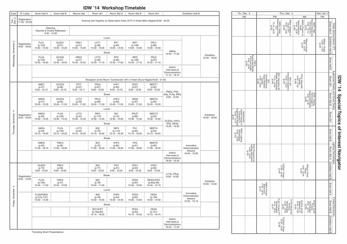
IDW ’14 Workshop TimetableDate 2F Lobby Snow Hall A Snow Hall B Marine Hall Room 301 Room 302 A Room 302 B Room 201 Exhibition Hall B
Tue.
,D
ec. 2 Registration
17:00 - 20:00 Evening Get-Together at Observation Deck (31F) in Hotel Nikko Niigata18:00 - 20:00
Wed
nesd
ay, D
ecem
ber
3
Registration8:00 - 18:00
Opening, Keynote & Invited Addresses
9:30 - 12:30
Lunch
Exhibition12:40 - 18:00
FLX1(p.102)
14:00 - 15:40
OLED1(p.67)
14:00 - 15:20
FMC1(p.51)
14:00 - 15:20
LCT1(p.38)
14:00 - 15:05
EP1(p.90)
14:00 - 14:50
INP1(p.108)
14:00 - 15:30
PRJ1(p.86)
14:00 - 15:30AMDp
14:00 - 17:00Break
FLX2(p.103)
15:45 - 16:25
OLED2(p.67)
15:45 - 16:45
FMC2(p.51)
15:45 - 16:45
LCT2(p.38)
15:45 - 17:10
EP2(p.90)
15:45 - 17:00
INP2(p.109)
15:45 - 17:15
PRJ2(p.87)
15:45 - 17:15
Author Interviews &
Demonstrations17:15 - 18:15
Reception at the Room “Continental” (4F) in Hotel Okura Niigata19:00 - 21:00
Thu
rsda
y, D
ecem
ber
4
Registration8:00 - 18:00
AMD1(p.47)
9:00 - 10:15
OLED3(p.68)
9:00 - 10:10
EP3†
(p.91)9:00 - 10:11
PRJ3(p.87)
9:00 - 10:05
VHF1(p.80)
9:00 - 10:10
DES1(p.97)
9:00 - 10:35
MEET1(p.92)
9:00 - 10:30FMCp, PHp,
3Dp, FLXp, INPp9:00 - 12:00
Exhibition10:00 - 18:00
Break
AMD2(p.47)
10:45 - 12:20
OLED4(p.69)
10:45 - 11:55
LCT3(p.39)
10:45 - 11:55
PRJ4(p.88)
10:45 - 11:50
VHF2(p.80)
10:45 - 11:55
DES2(p.97)
10:45 - 11:55
MEET2(p.93)
10:45 - 12:45
Lunch
AMD3(p.48)
13:30 - 14:55
FLX3(p.105)
13:30 - 14:45
LCT4(p.40)
13:30 - 14:35
INP3(p.110)
13:30 - 14:20
3D1(p.75)
13:30 - 15:00
PRJ5†
(p.88)13:30 - 14:42
MEET3(p.94)
13:30 - 14:50OLEDp, VHFp,
EPp, DESp13:30 - 16:30
Break
AMD4(p.49)
15:15 - 16:20
FLX4(p.105)
15:15 - 16:25
LCT5(p.40)
15:15 - 16:20
3D2(p.76)
15:15 - 16:30
INP4(p.110)
15:15 - 16:30
PH1(p.60)
15:15 - 16:25
MEET4(p.94)
15:15 - 16:55
Break
InnovativeDemonstration
Session16:45 - 19:30
AMD5(p.49)
17:00 - 18:10
FMC3(p.56)
17:00 - 18:00
3D3(p.76)
17:00 - 18:40
VHF3(p.82)
17:00 - 18:00
PH2(p.61)
17:00 - 18:05
MEET5(p.95)
17:00 - 18:40
Author Interviews &
Demonstrations18:30 - 19:30
Frid
ay, D
ecem
ber
5
Registration8:00 - 13:00
OLED5(p.73)
9:00 - 10:25
FMC4(p.56)
9:00 - 10:00
3D4(p.77)
9:00 - 10:20
PH3(p.61)
9:00 - 10:25
FED1(p.63)
9:00 - 10:35
VHF4(p.83)
9:00 - 10:00LCTp, PRJp9:00 - 12:00
Exhibition10:00 - 14:00
Break
FLX5(p.106)
10:45 - 11:50
FMC5(p.57)
10:45 - 12:05
3D5(p.78)
10:45 - 11:45
FED2(p.64)
10:45 - 12:05
DES3/VHF5(p.83/p.99)
10:45 - 12:15
LunchInnovative
Demonstration Session
12:30 - 15:15
FLX6/FMC6(p.57/p.107)
13:30 - 14:35
3D6(p.78)
13:30 - 14:55
VHF6(p.84)
13:30 - 14:30
FED3(p.65)
13:30 - 14:50
DES4(p.100)
13:30 - 14:30
Break
3D7/VHF7(p.79/p.85)
15:15 - 16:20
FED4(p.65)
15:15 - 16:35
DES5(p.101)
15:15 - 16:15
Author Interviews &
Demonstrations16:45 - 17:45
†Including Short Presentations
Oxide-S
emiconductor T
FT
Augm
ented Reality and V
irtual Reality
Lighting TechnologiesP
rinted Electronics
Snow
Hall A
Exhibition H
all BS
now H
all BR
oom 301
Room
302 BR
oom 201
Snow
Hall B
Room
302 AE
xhibition Hall B
Snow
Hall A
Snow
Hall B
Exhibition H
all BWed., Dec. 3
PM
AM
Dp1: P
oster14:00 - 17:00
(p.22)
Thu., Dec. 4AM
AM
D1: H
igh Resolution Displays Using
LTPS & Oxide TFTs9:00 - 10:15
(p.24)F
MC
p4: Poster
9:00 - 12:00(p.24)
DE
S1: D
isplay Technologies in
Augm
ented Reality
9:00 - 10:35(p.28)
FM
Cp3, P
Hp2:
Poster
9:00 - 12:00(p.32)
OLE
D3: O
LED
P
rocess Technologies9:00 - 10:10
(p.35)
AM
D2: P
hysics of O
xide S
emiconductors
10:45 - 12:20(p.25)
PR
J4: Wearable
Display
10:45 - 11:50(p.28)
OLE
D4: O
LED
M
aterials (1)10:45 - 11:55
(p.35)
PM
AM
D3: S
tability of O
xide TF
T13:30 - 14:55
(p.26)
INP
3: AR
Interactive S
ystems
13:30 - 14:20(p.29)
OLE
Dp1: P
oster13:30 - 16:30
(p.33)
FLX
3: Advanced
Printing
Technologies13:30 - 14:45
(p.36)O
LED
p2: Poster
13:30 - 16:30(p.36)
AM
D4: H
igher P
erformance O
xide T
FT
15:15 - 16:20(p.26)
3D2: Interactive 3D
D
isplay Technology15:15 - 16:30
(p.29)
FLX
4: Printed T
FT
Technologies15:15 - 16:25
(p.37)
3D3:
Om
nidirectional H
yper-Realistic
System
17:00 - 18:40(p.30)
AM
D5: P
rinted E
lectronics17:00 - 18:10
(p.37)
Fri., Dec. 5AM
FM
C4:
Augm
ented Reality
& V
irtual Reality
9:00 - 10:00(p.30)
PH
3: Phosphors for
Lighting Application
9:00 - 10:25(p.33)
DE
S3/V
HF
5: S
ystem D
esign &
Evaluation in
Augm
ented Reality
10:45 - 12:15(p.31)
FM
C5: Lighting
Technologies10:45 - 12:05
(p.34)
IDW
’14 Sp
ecial Top
ics of In
terest Navig
ator

IDW ’14 Session NavigatorWednesday, December 3 Thursday, December 4 Friday, December 5
PM 17:15-18:15 AM PM 18:30-19:30 AM PM 16:45-17:45
Active-Matrix Displays
Exhibition Hall B Snow Hall A Exhibition Hall B
PostersHigh Resolution
Displays Using LTPS & Oxide TFTs
Physics of Oxide Semiconductors Stability of Oxide TFT Higher Performance
Oxide TFT Printed Electronics A.I.
Display Electronic Systems
Room 302 B Exhibition Hall B Exhibition Hall B Room 201 Exhibition Hall B
Display Technologies in Augmented Reality Image Processing Posters A.I.
System Design & Evaluation in
Augmented Reality*
Display Driving Technologies
Display Interface & Driving Technologies A.I.
Emissive Technologies
Room 201 Exhibition Hall B Room 302 B Exhibition Hall B Room 302 B Exhibition Hall B
Solid-State Light Source Technologies for
ProjectorPosters Phosphor for General Phosphor
Applications A.I. Novel Devices & Applications
Fabrication Processes & New
Materials
FE Mechanisms & PDP Protective
Layers
Summing Up of PDP History A.I.
Room 302 A Snow Hall B
Phosphors for Lighting Application Lighting Technologies
e-Paper
Room 302 A Exhibition Hall B Marine Hall Exhibition Hall B Exhibition Hall B
Electrophoretic Displays
Various Technologies for e-Paper A.I. Chromic Displays Posters A.I.
Flexible Electronics
Snow Hall A Exhibition Hall B Exhibition Hall B Snow Hall B Exhibition Hall B Snow Hall A Exhibition Hall B
Flexible Backplane Flexible Displays & Devices A.I. Posters Advanced Printing
TechnologiesPrinted TFT
Technologies A.I. Flexible Substrates Flexible Materials & Devices* A.I.
Image Quality Evaluation & Human Factor
Room 302 A Exhibition Hall B Room 302 A Exhibition Hall B Room 201 Room 302 A Room 301 Exhibition Hall B
Optical Measurements Color & OLEDs Posters Moving Image Quality A.I. Display Legibility
System Design & Evaluation in
Augmented Reality*
Mobile Human Factors & 'Kansei'
Evaluation
Visual Perception for 3D System* A.I.
Liquid-Crystal Technologies
Room 301 Exhibition Hall B Marine Hall Exhibition Hall B Exhibition Hall B
Fast Switching LCD Novel Optics for LCD A.I. Photo Alignment LC Materials LC Evaluation A.I. Posters
Manufacturing, Process & Equipment
Marine Hall Exhibition Hall B Exhibition Hall B
Manufacturing Technologies A.I. Posters
Materials & Components
Marine Hall Exhibition Hall B Exhibition Hall B Snow Hall B Exhibition Hall B Snow Hall B Snow Hall A Exhibition Hall B
Materials & Components A.I. Posters Optical Films A.I. Augmented Reality
& Virtual Reality Lighting Technologies Flexible Materials & Devices* A.I.
MEMS & Nanotechnologies
Room 201 Exhibition Hall B
Emerging Quantum Dots &
Nanotechnologies
Fundamental Components & Process Technologies
EL Quantum Dots Technologies
Novel Materials & Components
Nanotechnology Display & Imaging A.I.
Organic Light-Emitting Displays & Organic Devices
Snow Hall B Exhibition Hall B Snow Hall B Exhibition Hall B Exhibition Hall B Snow Hall A Exhibition Hall B
Advanced OLED Technologies (1)
Advanced OLED Technologies (2) A.I. OLED Process
Technologies OLED Materials (1) Posters A.I. OLED Materials (2) A.I.
Projection & Large Area Displays
Room 201 Exhibition Hall B Room 301 Room 302 B Exhibition Hall B Exhibition Hall B
Solid-State Light Source Technologies for
ProjectorVehicle Display A.I. Projection
Technologies Wearable Display Projection Applications A.I. Posters
Touch & Interactive Technologies
Room 302 B Exhibition Hall B Exhibition Hall B Room 301 Room 302 A Exhibition Hall B
Touch Panel (1) Touch Panel (2) & Haptics A.I. Posters AR Interactive
SystemsSensor &
Applications A.I.
3D/Hyper-Realistic Displays
Exhibition Hall B Room 302 A Room 301 Exhibition Hall B Room 301 Exhibition Hall B
Posters Holography Interactive 3D Display Technology
Omnidirectional Hyper-Realistic
SystemA.I. 3D/Hyper-Realistic
Displays (1)3D/Hyper-Realistic
Displays (2)Optical Devices for
3D SystemVisual Perception for
3D System* A.I.
A.I. Author Interviews & Demonstrations* Joint Session

IDW
’14
Th
e 21
st In
tern
atio
nal
Dis
pla
y W
ork
sho
ps
Dec
embe
r 3-
5, 2
014
TOK
I ME
SS
E N
iigat
a C
onve
ntio
n C
ente
r, N
iigat
a, J
apan
Reg
istr
atio
n
Acc
om
mo
dat
ion
s
(1)
Reg
istr
atio
n F
ees
Th
e r
eg
istr
ati
on
fe
e i
ncl
ud
es
ad
mis
sio
n t
o t
he
co
nfe
ren
ce a
nd
a
CD
-RO
M o
f the
pro
ceed
ings
. In
addi
tion,
a p
rinte
d F
inal
Pro
gram
incl
udin
g ab
stra
cts
of e
ach
pape
r w
ill b
e pr
ovid
ed a
t the
con
fere
nce
site
. No
refu
nds
will
be
mad
e on
and
afte
r N
ovem
ber
1, 2
014.
*1 A
SO
: A
cade
mic
Sup
port
ing
Org
aniz
atio
ns.
See
p.1
4 as
wel
l as
“S
uppo
rtin
g O
rgan
izat
ions
an
d S
pons
ors”
at
th
e en
d of
ea
ch
wor
ksho
p se
ctio
n in
the
Adv
ance
Pro
gram
.*2
Indi
vidu
al m
embe
r*3
If
you
inte
nd t
o jo
in e
ither
IT
E o
r S
ID,
the
one
year
mem
bers
hip
fee
will
be
subs
idiz
ed b
y th
e ID
W ’1
4 C
omm
ittee
.*4
Pho
toco
py o
f you
r st
uden
t ID
is r
equi
red.
(2)
Rec
epti
on
Fee
Unt
il O
ctob
er 3
1 ¥
8,00
0
On
and
Afte
r Nov
embe
r 1
¥10,
000
One
free
tick
et w
ill b
e pr
ovid
ed to
eac
h in
vite
d sp
eake
r.
(3)
Ad
dit
ion
al P
roce
edin
gs
(CD
-RO
M)
At t
he C
onfe
renc
e Si
te
¥8,
000
Airm
ail a
fter t
he C
onfe
renc
e ¥1
2,00
0
Dom
estic
Mai
l afte
r the
Con
fere
nce
¥10,
000
Reg
istr
atio
n
(1)
e-R
egis
trat
ion
(Dea
dlin
e: N
ovem
ber
21, 2
014)
Acc
ess
http
://w
ww
.idw
.or.
jp/r
egis
t.htm
l
(2)
Mai
l or
Fax
(D
eadl
ine:
Nov
embe
r 21
, 201
4)
Reg
istr
atio
n F
orm
is a
vaila
ble
via
http
://w
ww
.idw
.or.
jp/r
egis
t.htm
l
(3)
On-
site Ea
rly-B
ird F
ee: u
ntil
Oct
. 31
Dea
dlin
e of
Adv
ance
Reg
istra
tion:
Nov
. 21
Dea
dlin
e of
Hot
el R
eser
vatio
n:N
ov. 1
4
JTB
Kan
to C
orp.
will
han
dle
arra
ngem
ents
for
your
hot
el r
eser
vatio
ns.
Roo
m r
ates
incl
ude
brea
kfas
t, se
rvic
e ch
arge
, and
8%
con
sum
ptio
n ta
x.
Can
cella
tio
n P
olic
y8
days
or
mor
e da
ys p
rior
to th
e fir
st n
ight
of s
tay
2 to
7 d
ays
befo
re th
e fir
st n
ight
of s
tay
1 da
y be
fore
the
first
nig
ht o
f sta
yB
efor
e 14
:00
of th
e fir
st n
ight
of s
tay
Afte
r 14:
00 o
f the
firs
t nig
ht o
f sta
y or
no
notic
e gi
ven
Res
erva
tio
nA
cces
s ht
tp://
ww
w.id
w.o
r.jp
/acc
omm
odat
ion.
htm
l
......
.....
No
char
ge...
......
.. 20%
of d
aily
roo
m r
ate
......
.....
40%
of d
aily
roo
m r
ate
......
.....
50%
of d
aily
roo
m r
ate
......
.....
100%
of d
aily
roo
m r
ate
Unt
ilO
ctob
er31
¥35,
000
¥45,
000
¥45,
000
¥55,
000
¥ 8
,000
¥10,
000
¥ 8
,000
¥10,
000
On
and
After
Nov
embe
r1
Stud
ent*
4N
on-
Mem
ber*
3
ITE/
SID
/A
SO*1
Mem
ber*
2
Life
Mem
ber o
fIT
E/SI
D
Hot
el N
ikko
Niig
ata
AN
A C
row
ne P
laza
Niig
ata
Band
ai S
ilver
Hot
el
Hot
el O
kura
Niig
ata
Niig
ata
Gra
nd H
otel
Niig
ata
Toky
u In
n
Hot
el S
unro
ute
Niig
ata
Niig
ata
Toei
Hot
el
Cou
rt H
otel
Niig
ata
Com
fort
Hot
el N
iigat
a
+81-
25-2
40-1
888
+81-
25-2
45-3
333
+81-
25-2
43-3
711
+81-
25-2
24-6
111
+81-
25-2
28-6
111
+81-
25-2
43-0
109
+81-
25-2
46-6
161
+81-
25-2
44-7
101
+81-
25-2
47-0
505
+81-
25-2
42-0
611
¥9,5
00
¥12,
500
¥8,0
00
¥8,5
00
¥8,0
00
¥7,5
00
¥7,5
00
¥6,5
00
¥6,0
00
¥6,0
00
Free
Free
Free
Free
Free
Free
Free
Free
Free
Free
Wire
less
Both
Both
Wire
less
Both
Both
Both
Both
Both
Both
¥9,0
00
¥8,7
00
¥7,5
00
¥8,0
00
¥7,5
00
¥6,5
00
¥6,5
00
¥6,0
00
Are
aH
otel
Nam
ePh
one
Sing
leTw
inC
harg
eW
ired
orW
irele
ss L
AN
Rate
s (p
er p
erso
n/ p
er n
ight
)In
tern
et A
cces
sN
o. in
map
(p18
)
1 2 3 4 5 6 7 8 9 10
Band
aiA
rea
Furu
mac
hiA
rea
Niig
ata
Eki
Mae
Are
a

THE 21ST INTERNATIONALDISPLAY WORKSHOPS
TOKI MESSE Niigata Convention CenterNiigata, Japan
December 3 – 5, 2014
Advance Program
Special Topics of Interest on• Oxide-Semiconductor TFT• Augmented Reality and Virtual Reality• Lighting Technologies• Printed Electronics
Workshops on• LC Science and Technologies (LCT)• Active Matrix Displays (AMD)• FPD Manufacturing, Materials and Components (FMC) • EL Displays and Phosphors (PH)• Field Emission Displays, CRTs and Plasma Displays (FED)• OLED Displays and Related Technologies (OLED)• 3D/Hyper-Realistic Displays and Systems (3D)• Applied Vision and Human Factors (VHF)• Projection and Large-Area Displays and Their Components (PRJ)• Electronic Paper (EP)• MEMS and Emerging Technologies for Future Displays and Devices (MEET) • Display Electronic Systems (DES)• Flexible Electronics (FLX)• Touch Panels and Input Technologies (INP)
IDW ’14
IDW
’14
Sec
reta
riat
:c/
o B
ilin
gu
al G
rou
p L
td.
3-3-
6 K
ud
an M
inam
i, C
hiy
od
a-ku
,To
kyo
102
-007
4, J
apan
Ph
on
e: +
81-3
-326
3-13
45
FAX: +
81-3
-326
3-12
64E
-mai
l: id
w@
idw
.or.
jp
htt
p:/
/ww
w.id
w.o
r.jp
/
IDW
’14
ADVA
NCE
PROG
RAM