Temporary Bond Material and Process: Survey Drivers and ... · 5 August 2011 2 Outline • 3D TSV...
14
Accelerating the next technology revolution Copyright ©2010 SEMATECH, Inc. SEMATECH, and the SEMATECH logo are registered servicemarks of SEMATECH, Inc. International SEMATECH Manufacturing Initiative, ISMI, Advanced Materials Research Center and AMRC are servicemarks of SEMATECH, Inc. All other servicemarks and trademarks are the property of their respective owners. Temporary Bond Material and Process: Survey Drivers and Reference Flow SEMICON WEST Temporary Bonding Workshop July 11th, 2011 Sitaram Arkalgud / MJ Yim
Transcript of Temporary Bond Material and Process: Survey Drivers and ... · 5 August 2011 2 Outline • 3D TSV...
Accelerating the next technology revolution
Copyright ©2010 SEMATECH, Inc. SEMATECH, and the SEMATECH logo are registered servicemarks of SEMATECH, Inc. International SEMATECH Manufacturing Initiative, ISMI, Advanced Materials Research Center and AMRC are servicemarks of SEMATECH, Inc. All other servicemarks and trademarks are the property of their respective owners.
Temporary Bond Material and Process: Survey Drivers and Reference Flow
SEMICON WEST Temporary Bonding WorkshopJuly 11th, 2011Sitaram Arkalgud / MJ Yim

5 August 2011 2
Outline
• 3D TSV Outlook• 3D TSV Integration Reference Flow and
Temporary Bonding Challenges/Survey Drivers

5 August 2011 3
3D options (ref: 2009 ITRS)
• 3D system-in-package– Eg: wire bonding, package-
on-package• 3D wafer-level packaging
– TSVs used at bond pads– Eg: stacked memory, CIS
• 3D global interconnects– Stacked IC, 3D system-on-
chip, “through silicon stacking”
– TSVs connect circuit blocks at the global wiring level
• 3D intermediate interconnects– Higher density than global– Interconnects smaller circuit
blocks• Local (device) level
– Transistor level stackingK Saraswat Stanford U.
Courtesy: Samsung.
Source: Qualcomm
Source: IBM
Source: Samsung
Source: Intel

5 August 2011 4
3D TSV Outlook
• Near future (2011 - 2013)– Interposer products – Wide IO DRAM (mobile)
• Future (2013 - 2017)– Heterogenous integration (beyond memory on logic)– Higher (>> 5 stacking levels)– Smaller (<< 5 micron width, >> 10 aspect ratio)
• Far future (2017 - 2025)– Beyond CMOS (photonics, sensors, etc)
Source: Xilinx Source: Nokia

5 August 2011 55 August 2011 5
Schematic Of Wide IO TSV Product (Source: Nokia, Qualcomm)
• Other products and integrations exist
• Wide IO provides context for SEMATECH development work
• Tier 2 could be a single die or multiple dies (Eg: a 4-tier Wide IO DRAM stack)
Tier 1Thickness ~ 50 µmActive Face Down
BackSide MetalPitch ~ 5-25 µm
Package SubstrateThickness ~ 100’s of µm
UnderfillGap ~ hi 10’s of µm
Flip Chip BumpSize ~ <100 umPitch ~ 100-200 um
TSVSize ~ 5-10 µmPitch ~ 10-50 µm
BGA BumpPitch ~ 1mm
µ-BumpPitch ~ 25-50 µm
UnderfillGap ~ 10 µm
Tier 2Thickness ~ 100 µmActive Face Down
Graphics adapted from R. Radojcic, Qualcomm
Focus area for SEMATECH

5 August 2011 6
Various Key Process Modules and 3D-stacking Options (source: ITRS 2009, ISMI 2009)

5 August 2011 7
Issues
Industry Reference Flows and Temporary Bonding Adhesive Challenges
Carrier wafer
Adhesive coating
Wafer bonding
TSV process
De-bonding
Final bonding
• Back-grind
• Cu reveal
• Passivation
• Planarization
• RDL/Bumping
• De-bondingThermal/chemical/ UV laser release
• Cleaning
Option 1 (WtW) Option 2 (WtW)
• Glass or Si
Thickness tolerance
No residual solvent
Void free
• Cu-Cu
• Cu-Sn-Cu w/ WLUF
Process Flow
Large TTV & chipping
Side etching
Delamination
Void & Delamination
Alignment
Warpage
Void & Delamination
Bump deformation
Residue
• Spin coating
• Bake
• T/T/P
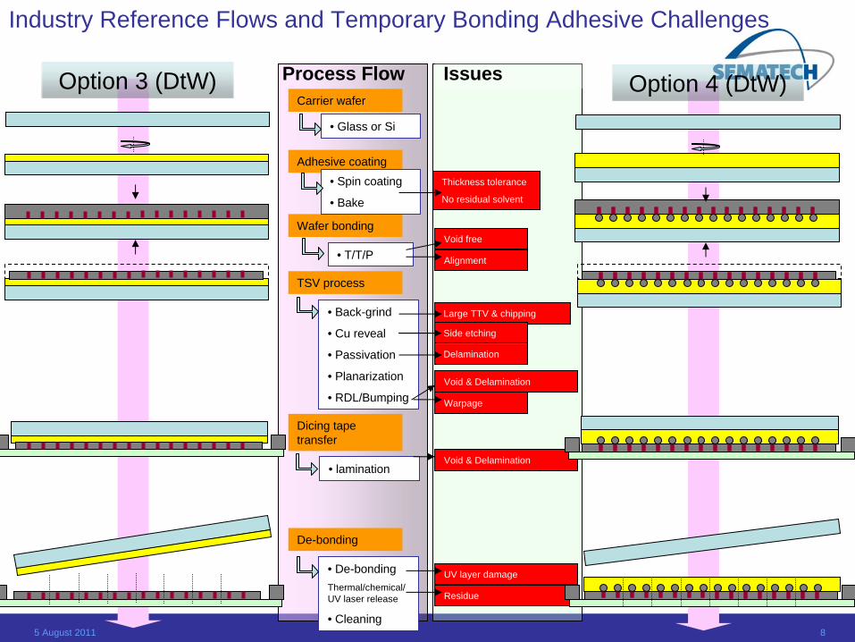
5 August 2011 8
IssuesCarrier wafer
Adhesive coating
Wafer bonding
TSV process
De-bonding
Dicing tape transfer
• Back-grind
• Cu reveal
• Passivation
• Planarization
• RDL/Bumping
• De-bondingThermal/chemical/ UV laser release
• Cleaning
Option 3 (DtW)
• Glass or Si
Thickness tolerance
No residual solvent
Void free
• lamination
Process Flow
Large TTV & chipping
Side etching
Delamination
Void & Delamination
Alignment
Warpage
Void & Delamination
UV layer damage
Residue
• Spin coating
• Bake
• T/T/P
Option 4 (DtW)
Industry Reference Flows and Temporary Bonding Adhesive Challenges

5 August 2011 9
Reference Flow Options
– Sematech 3D baseline: DtW, bumpless, Cu-Cu– Reference flow options
• Logic TSV (DtS)=>Memory cube to Logic TSV (DtD)=>Backend (Molding/BA/singulation)
memorymemorymemorymemory
Logic
Logic die w/NCF (C4 bump face down)
C4 process for Tier 1 Molding, etc Tier 2 Die to Tier 1 die attach process (T/C bonding)
Option 4
Option 2 or 4
Option 3
Various temporary bonding/debonding supports are required for WtW and DtW processes.

5 August 2011 10
Temporary Bond Process Flow Issues
• Thickness• Uniformity
• Room Temp?• Method• Throughput
APPLY ALIGN & BOND DEBOND CLEAN
• < 10 um• Room Temp?• Bond Strength
• C4 or ubump ?• Cleaning• chemical at dicing tape?
• up to what max. temp?• Chemicals• Grind/polish• Handling
WAFER PAIRPROCESSING
ISSUE / CHALLENGE
• Thermal
• UV / Laser
• Mechanical
• Chemical
• Zone
METHODS • Spin coat
• Laminate
• Zone
• Combination
• Thermal
• UV
• Combination
• Spray
• Immersion
• Plasma
• Combination
Process Requirements Must be Established to Identify Temporary Bond Materials (adhesive and carrier) as well as Associated Debond Methods

5 August 2011 11
3D Temporary Bonding Adhesive Requirements• Si or glass carrier wafer compatible• Protect the topography of the device wafer
– Bumped (C4 or micro-bumped) or non-bumped wafers– 5 um TTV (thin adhesive and thick adhesive)
• Strong enough to withstand wafer backside process– Thermally stable to withstand backside process– Chemically stable to withstand backside process
• Easily de-bonded• Residue free
– Device wafer side & carrier wafer side for re-use
• Other thermo-mechanical properties considerations– Low out-gassing, low or higher modulus for low stress and warpage,
etc

5 August 2011 12
Temporary Bonding Materials
• These temporary bonding materials are generally chemically stable to temperatures of 250 ºC, above which some decomposition or out-gassing occurs
• Broad range of process conditions depending on materials and bonding/de- bonding methods
– Bonding method: thermal (High, Medium or Low temperature) or UV or others?– De-bonding method: Room to Low, Medium or High temperature de-bonding?– Adhesive thickness: any thickness guideline?– Thermal stability during TSV backside processes and permanent bonding– Cleaning chemical??
• How to differentiate the materials is primarily dependant to (1) TSV applications, (2) backside process conditions, (3) release process conditions and where to release, etc
– Real temporary adhesive material capabilities should be evaluated not only by back end process temperatures, but also by other factors including time at those temperatures, the presence of a vacuum or pressure environment, energy level in a PECVD, and the residual wafer stress at elevated temperature

5 August 2011 13
Bond Material Application Space
Thermal stability (oC)
De-
bond
ing
tem
p (o
C)
200 300 400
100
200
300
400
100
Sn-based Solder Liquidis Start
Max Process Temp. of Materials in Bumpless Flow
Thermal Stability of Dicing Tape(desired debond temperature is 25 C)
500
Bond Material and Debond Process Must Satisfy Process Requirements SpaceLimited options if high temp processing & low temp debonding needed
BumplessBumped
Max Process Temp. of Materials in Bumped Flow Zone Debond
Thermal Slide-off
Chemical de-bond
ABCD
E
F
Adhesives
Debond Process
G
Mechanical de-bond
Laser De-bond
H

5 August 2011 14
Industry User Community Survey• Temporary Bonding / Debonding Landscape Unsettled
– Process / Material Selection Dependent on Reference Flow– Material and Tool Suppliers offer multiple solutions
• 3D TSV Reference Flow Critical to Identifying Consensus Solution– Limited Feedback suggests a desire for room temperature bond and debond processes with an
adhesive material which can withstand temperatures of up to 400C
• Build Consensus– Temporary Bonding / Debonding is an ENABLING technology; lowering costs requires broad
acceptance of application requirements– Industry User Survey to help set technical requirements of Temporary Bond Materials and Debond
Process; validation of reference flow approach
• Accelerate Innovation and Collaboration– Identify supplier partners to develop temporary bond solutions.