Technology Overview - VESA
25
iDP TM (Internal DisplayPort TM ) Technology Overview New Generation Large-Screen Display Internal Interface DisplayPort Developer Conference | December 6, 2010 | Westin Taipei Alan Kobayashi R&D Director, DisplayPort Solutions, TVM, STMicroelectronics VESA Board of Director Editor of DisplayPort Task Group Chair/Editor of TV Panel Task Group
Transcript of Technology Overview - VESA

iDPTM (Internal DisplayPortTM) Technology Overview
New Generation Large-Screen Display Internal Interface
DisplayPort Developer Conference | December 6, 2010 | Westin Taipei
Alan Kobayashi
R&D Director, DisplayPort Solutions, TVM, STMicroelectronics
VESA Board of Director Editor of DisplayPort Task Group Chair/Editor of TV Panel Task Group

2
Contents
Ø Display Port Family Ø Why iDP
Ø iDP PHY Layer
Ø iDP Link Layer
Ø Comparison between Constant and Variable Link Rate

3
Display Controller Board
TCON Board
iDP
• DP (DisplayPort) - Connection to TV, Monitors from an external source
• eDP (embedded DP) - Connection between GFx and notebook panel
• iDP (internal DP) - Connection between Display controller and TCON within a large-screen display (e.g., DTV display)
DP
DP
eDP
DisplayPort Family

4
DisplayPort Family (as of DEC 2010) DP1.2 eDP iDP
Standard VESA V1.2 Jan 2010
VESA V1.2: May 2010
VESA : iDP1.0 Released Apr 2010
PHY AC Coupled / CDR / ANSI 8b/10b
Bandwidth (per lane) HBR2 5.4Gbps HBR 2.7Gbps RBR 1.62Gbps
HBR 2.7Gbps RBR 1.62Gbps
Nominal 3.24Gbps/lane Other link rates: Implementation Choice (e.g., 3.78Gbps/lane)
Lane Count 1, 2, or 4 lanes 1. 2, or 4 lanes 1 ~ 16 lanes per bank
Secondary Data Packet
YES Optional NO
AUX CH YES (incl.vUSB2.0 transport over AUX)
Optional (used for backlight/ color control)
NO
HPD YES
Optional YES (Used for Link Training Pattern transmission trigger)
Transported data Multiple A/V streams Control data
Video Stream Control data
Video Stream
Stream Clocking Mode
Synchronous or Asynchronous to Link Symbol Clock Synchronous only; Nvid fixed to 48 decimal
Target Application Box2Box connection to TV/Monitor with Multi-stream
Internal to Notebook/Netbook /Notepad/All-in-one PC
Internal to TV/monitor chassis

5
iDP Compliance Test Guideline Document Ø Companion guideline document to iDP Standard
Specification V1.0 Ø Describes compliance test methods for a source device, a
sink device, and a cable/connector assembly
Ø Covers PHY and Link Layer compliance testing
Ø Applicable to 3.24Gbps/lane and other link rates such as 3.78Gbps/lane
Ø Lists reference connector pin-outs
Ø 41 pin for 4 lanes (also used for a test fixture)
Ø 51 pin for 8 lanes
Ø Expected to be published in DEC 2010 ~ JAN 2011

6
Why iDP ?
2008
Ø Ever increasing TV applications demand for bandwidth
2012
FHD 60Hz
FHD 240Hz
4.5Gb/s 3D/120Hz
18Gb/s
18Gb/s
UD (4k x 2k)/120Hz
36Gb
9Gb/s
Ø Use of LVDS is becoming un-manageable Ø Signal integrity issues Ø Poor EMI performance Ø Too many connectors, wires, pins on TV SoC and T-CON Ø Cost

7
iDP Benefits
Ø Proven Technology in a various of applications Ø Most reliable and robust link based on proven DP technology
Ø Open and Royalty- Free Industry Standard
Ø International VESA Standard Ø VESA members free in contribution in Spec. / IP development
Ø Far fewer number of wires than LVDS
Ø Much lower EMI than LVDS
Ø Constant link rate for the utmost link stability

8
iDP vs. LVDS: Signal Count Comparison
LVDS FHD(10bit) 60Hz 120Hz 240Hz
No. of signals 24 48 96
Ø LVDS
Ø iDP: Based on nominal 3.24 Gbps/lane (Main Link plus HPD) iDP FHD(10bit)
60Hz 120Hz 240Hz
No. of signals 5 9 17

9
>60dB
EMI Peaks
-LVDS: from LVDS CLK=74.28MHz 2)
-Red Circles: from System Ref.CLK 3) 15dB~25dB Improvement
iDP vs. LVDS: EMI Data
From Sys.Ref.Clock not from iDP
1) With switching regulator in board
2) Blue Circles (LVDS) : EMI peaks from Pixel Clock and also from system clock
3) Red Circles (iDP): Only EMI from system clock
-Blue line : Horizontal Direction
-Red Line: Vertical Direction
Identical setup for iDP & LVDS
-1.0 meter FFC
-STM TX and RX Board
-5 Volts -AC Adaptor 1)
-Video Pattern: Blue/Grey Bar

iDP PHY Layer

11
CDR with ANSI 8B/10B Channel Coding
CPU/GPU Peripheral PCI Express/SATA
:ANSI 8B/10B & CDR
Internal Panel eDP 1)
:ANSI 8B/10B CDR
USB 3.0 2) :ANSI 8B/10B & CDR
Secondary Monitor DP 3)
ANSI 8B/10B & CDR
1) Now LVDS IF is transitioning to eDP. 2)Until USB 2.0:based on a half-duplex differential signaling 3) Apple /Lenovo /HP/Dell shipping MAC/PC with DP output for the external monitor interface
iDP Technology based on CDR with ANSI8B/10B, proven in data communication industry.
2 Box TV with DP [1080P 120Hz
Video/Audio/I2C over AUX]

12
iDP PHY Layer Sink Device
iDP PHY Electrical Sub-Layer
iDP PHY Layer taken from a proven DisplayPort design
CDR
◈ iDP PHY Layer a subset of DP1.2
EQ (Optional)
ANSI 8B/10B
iDP PHY Layer Source Device
GAIN/ Pre-EM

13
At high bit rates and/or over long distance, the signal degrades
Transmitter [Source]
Receiver [Sink]
Pre-Emphasis by iDPTX (Mandatory)
High Frequency or short bit
Low Frequency or long bit
Higher Voltage Swing on short bit [over long distance]
Transmitter [Source] Receiver [Sink]
Pre-emphasis helps facilitate clock recovery and symbol lock by a sink device via compensating for frequency-dependent insertion loss of channel

14
Channel Equalization by iDPRX (Optional)
Cable/FPC/PCB
Transmitter Receiver with Equalizer
Receiver input Receiver inside Transmitter output -

15 15
Ø Link Training Ø iDPRX prompts iDPTX to transmit link training pattern by
generating a low-going pulse
Ø Inter-lane skew Ø Two link symbols between adjacent lanes
Ø Data symbol scrambling Ø Seed value = FFFEh; same as eDP, different from DP
Ø ANSI8B/10B channel coding
iDP PHY Logical Sub-Layer
⎥⎦
⎤⎢⎣
⎡⎟⎠
⎞⎜⎝
⎛=4
LaneCount ofRemainder **2 cyclesLSClkLaneSkew
TPS1 TPS2 “normal operation” TPS1
HPD
Transmitted Data
tT1D
tHPL
tHPP
tT2D
tT2P_RX, TT2P_TX

iDP Link Layer

17
iDP Link Layer is a subset of the DP Standard: Far lighter
iDP Link Layer
iDP Link Layer Descriptions
SDP None Enabling the simplest Link Design
AUX None Enabling the simplest Link Design
Content Protection None Enabling the simplest Link Design
Clocking Mode Synchronous Nvid =48 dec and Mvid = 8 bits
Allowing the smallest pixel clock regeneration PLL
MSA Packet Only MISC0 and MISC1 bit7 and bit2:1 and H width and V height
Simplified, but supporting in-band signaling for stereoscopic 3D transport

18
Data Rate Throttling
Ø iDPTX, upon receiving pixel data from a stream source, throttles the pixel data rate
Ø Supports various pixel rates over constant-rate link with Nvid value fixed to 48 decimal
Ø Dependent on the buffer size in iDPTX, realizes horizontal blanking reduction transparently to a stream source and an iDPRX TCON
Active Video Period HBLANKStandard Video
Active Video Period (TU’s)Sea of Dummy
symbolsStandard iDP Video
Active Video Period (TU’s)Throttled iDP VideoSea of Dummy
symbols
Active Video Period
Active Video Period (TU’s)
Active Video Period (TU’s)

19
3D Supporting in iDP Standard
DP 1.1a DP 1.2
iDP1.0 supports inband signaling for stereoscopic 3D transport

Comparison between Constant Link Rate and Variable Link Rate

21
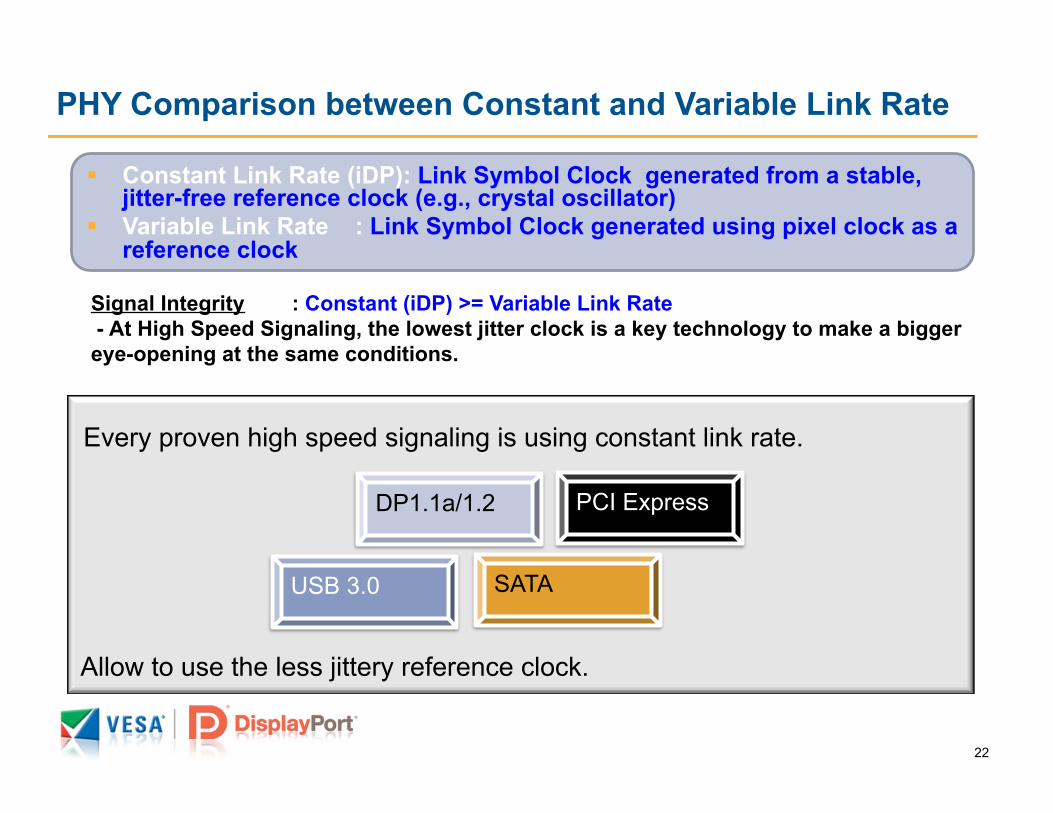
PHY Comparison between Constant and Variable Link Rate
PLL CDR
PH
Y Layer
PH
Y Layer
Recovered CLK
Variable Link Rate from Pixel Clock
Input Pixel CLK
Variable Link Rate
TCON w/ Variable Link Rate
=N*CLK
PLL PLL CDR
PH
Y Layer
PH
Y Layer
Recovered CLK
Constant Link Rates [iDP]
Ref.CLK
Nominal 3.24 Gbps Link Rate Or Higher
Link Rate= Q * RefClk =3.24 Gbps or higher RefClk from low jitter crystal
TV Controller w/ iDP Tx
TCON w/iDP Rx
=M/N*CLK
PLL LS CLK
SYS CLK
Ref.CLK
SYS CLK
LS CLK= N * InputPixelClk Input Pixel Clock bound to be jittery
TV Controller w/ Variable Link Rate
Constant Link Rate (iDP) Variable Link Rate
Architectural Concept From the optimized High Speed Signaling From Legacy Video Interface
Link Rates Pixel Clock Decoupled Pixel Clock Coupled tightly
Link Stability Steady and Uninterruptible Unstable and interruptible by Pixel Clock Variation/Change
22
Signal Integrity : Constant (iDP) >= Variable Link Rate - At High Speed Signaling, the lowest jitter clock is a key technology to make a bigger eye-opening at the same conditions.
§ Constant Link Rate (iDP): Link Symbol Clock generated from a stable, jitter-free reference clock (e.g., crystal oscillator)
§ Variable Link Rate : Link Symbol Clock generated using pixel clock as a reference clock
PCI Express
USB 3.0 SATA
DP1.1a/1.2
Every proven high speed signaling is using constant link rate.
Allow to use the less jittery reference clock.
PHY Comparison between Constant and Variable Link Rate

23
Maximum Link Rate : Constant (iDP) >= Variable Link Rate The jitter of reference clock defines the maximum link rate at high speed signaling , an Constant link rate can use less jittery reference clock at any scenario.
§ Constant Link Rate (iDP): Link Symbol Clock generated from a stable, jitter-free reference clock (e.g., crystal oscillator)
§ Variable Link Rate : Link Symbol Clock generated using pixel clock as a reference clock
USB 3.0 =5Gbps SATA = 6Gbps DP1.2 =5.4Gbps
Constant Link Rate (iDP) can support higher link rates at any scenario compared to a variable link rate( from a pixel clock).
Only iDP based on a proven technology.
PHY Comparison between Constant and Variable Link Rate

24
Link Stability during video format change: Constant (iDP) >> Variable Link Rate Pixel CLK is bound to change at any time in ATSC/DVB Application. Especially problematic for MEMC based 120-/240-Hz frame rate conversion algorithm implementation. With a variable link rate, the display should be turned off during channel / mode / input changes and it requires new Clock Recovery/Symbol Lock Sequence , if any pixel clock changes.
§ Constant Link Rate (iDP): Link Symbol Clock generated from a stable, jitter-free reference clock (e.g., crystal oscillator)
§ Variable Link Rate : Link Symbol Clock generated using pixel clock as a reference clock
Only iDP (Constant Link Rate) can allow a seamless transition during channel/mode/input changes including pixel frequency variations.
PHY Comparison between Constant and Variable Link Rate

THANK YOU