Technology advances in flexible displays and substrates
26
1
-
Upload
salman-khaja -
Category
Devices & Hardware
-
view
932 -
download
3
Transcript of Technology advances in flexible displays and substrates
1
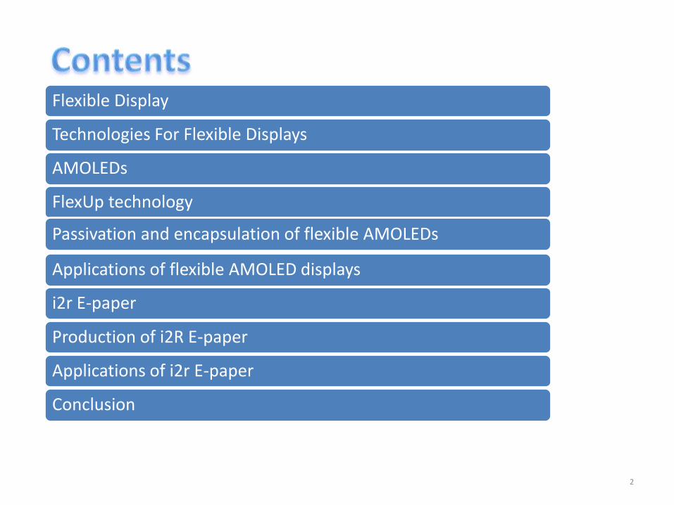
Flexible Display
Technologies For Flexible Displays
AMOLEDs
FlexUp technology
Passivation and encapsulation of flexible AMOLEDs
Applications of flexible AMOLED displays
i2r E-paper
Production of i2R E-paper
Applications of i2r E-paper
Conclusion
2
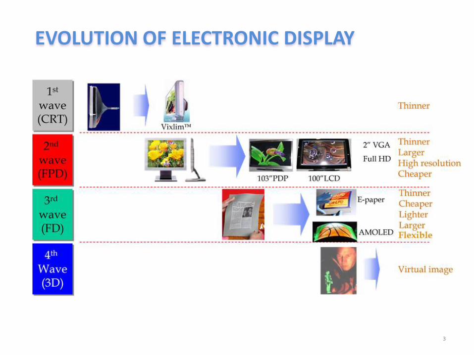
EVOLUTION OF ELECTRONIC DISPLAY
3
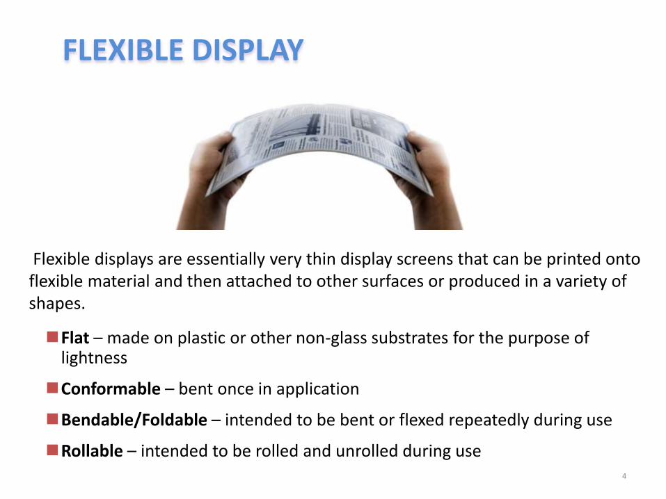
FLEXIBLE DISPLAY
Flexible displays are essentially very thin display screens that can be printed onto flexible material and then attached to other surfaces or produced in a variety of shapes.
4
Flat – made on plastic or other non-glass substrates for the purpose of lightness
Conformable – bent once in application
Bendable/Foldable – intended to be bent or flexed repeatedly during use
Rollable – intended to be rolled and unrolled during use
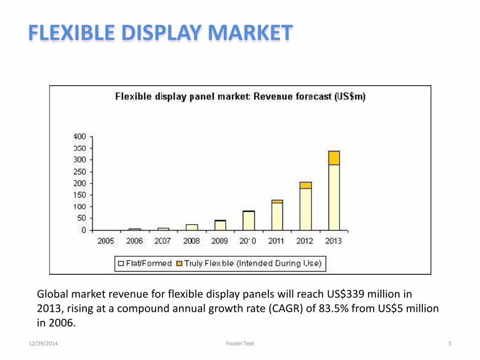
FLEXIBLE DISPLAY MARKET
12/29/2014 Footer Text 5
Global market revenue for flexible display panels will reach US$339 million in 2013, rising at a compound annual growth rate (CAGR) of 83.5% from US$5 million in 2006.
6
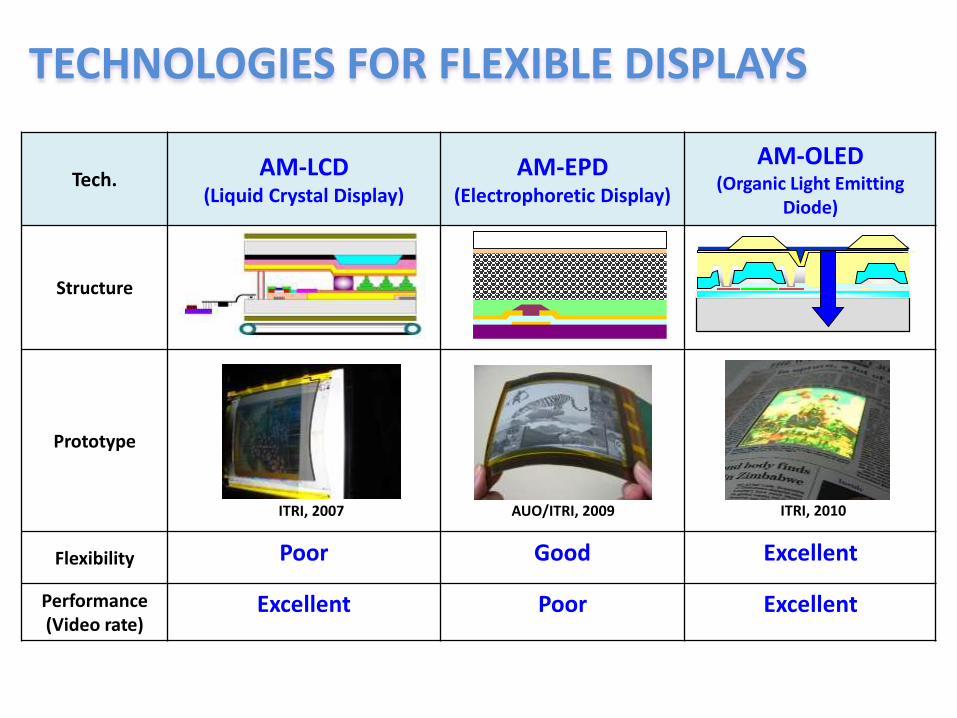
Tech.AM-LCD
(Liquid Crystal Display)
AM-EPD(Electrophoretic Display)
AM-OLED(Organic Light Emitting
Diode)
Structure
Prototype
Flexibility Poor Good Excellent
Performance(Video rate)
Excellent Poor Excellent
AUO/ITRI, 2009 ITRI, 2010ITRI, 2007
TECHNOLOGIES FOR FLEXIBLE DISPLAYS
7
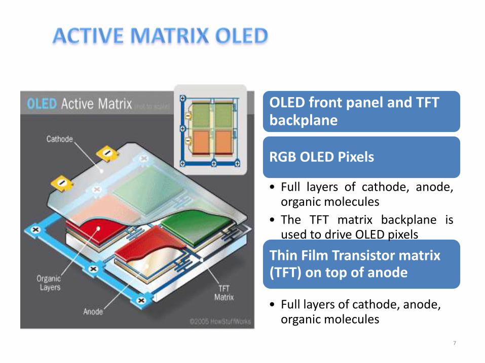
OLED front panel and TFT backplane
RGB OLED Pixels
• Full layers of cathode, anode, organic molecules
Thin Film Transistor matrix (TFT) on top of anode
• Full layers of cathode, anode,organic molecules
• The TFT matrix backplane isused to drive OLED pixels
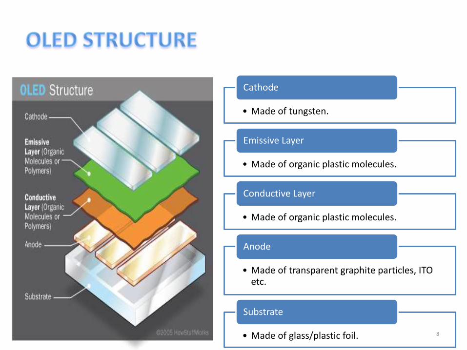
• Made of tungsten.
Cathode
• Made of organic plastic molecules.
Emissive Layer
• Made of organic plastic molecules.
Conductive Layer
• Made of transparent graphite particles, ITO etc.
Anode
• Made of glass/plastic foil.
Substrate
8
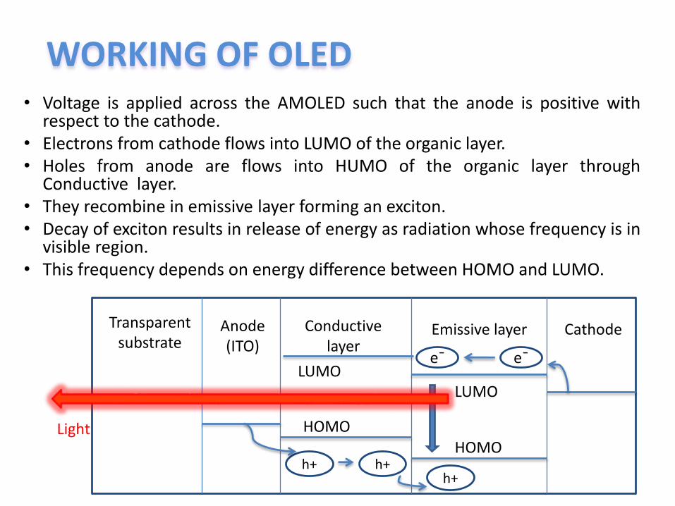
WORKING OF OLED• Voltage is applied across the AMOLED such that the anode is positive with
respect to the cathode.• Electrons from cathode flows into LUMO of the organic layer.• Holes from anode are flows into HUMO of the organic layer through
Conductive layer.• They recombine in emissive layer forming an exciton.• Decay of exciton results in release of energy as radiation whose frequency is in
visible region.• This frequency depends on energy difference between HOMO and LUMO.
Transparent substrate
Anode(ITO)
Conductive layer
Emissive layer Cathode
LUMOLUMO
HOMOHOMO
eˉeˉ
h+h+h+
Light
10
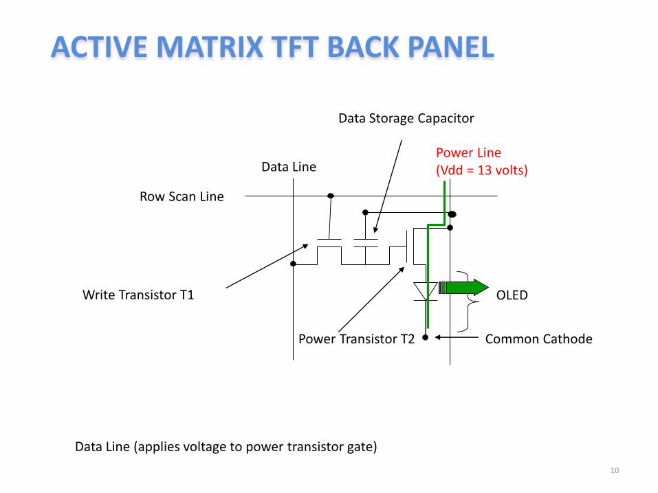
Data Line
Data Storage Capacitor
Power Transistor T2
Write Transistor T1
Data Line (applies voltage to power transistor gate)
Row Scan Line
Power Line(Vdd = 13 volts)
OLED
Common Cathode
ACTIVE MATRIX TFT BACK PANEL
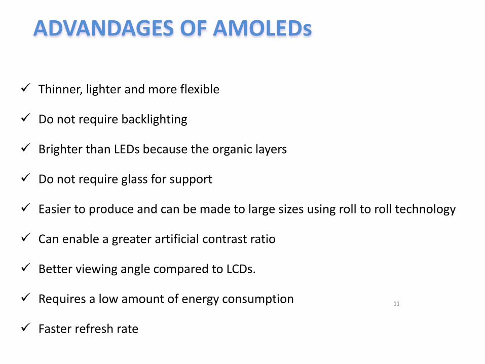
ADVANDAGES OF AMOLEDs
11
Thinner, lighter and more flexible
Do not require backlighting
Brighter than LEDs because the organic layers
Do not require glass for support
Easier to produce and can be made to large sizes using roll to roll technology
Can enable a greater artificial contrast ratio
Better viewing angle compared to LCDs.
Requires a low amount of energy consumption
Faster refresh rate
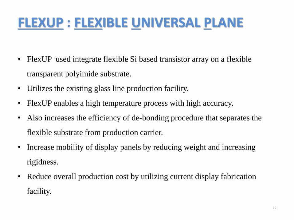
FLEXUP : FLEXIBLE UNIVERSAL PLANE
12
• FlexUP used integrate flexible Si based transistor array on a flexible
transparent polyimide substrate.
• Utilizes the existing glass line production facility.
• FlexUP enables a high temperature process with high accuracy.
• Also increases the efficiency of de-bonding procedure that separates the
flexible substrate from production carrier.
• Increase mobility of display panels by reducing weight and increasing
rigidness.
• Reduce overall production cost by utilizing current display fabrication
facility.
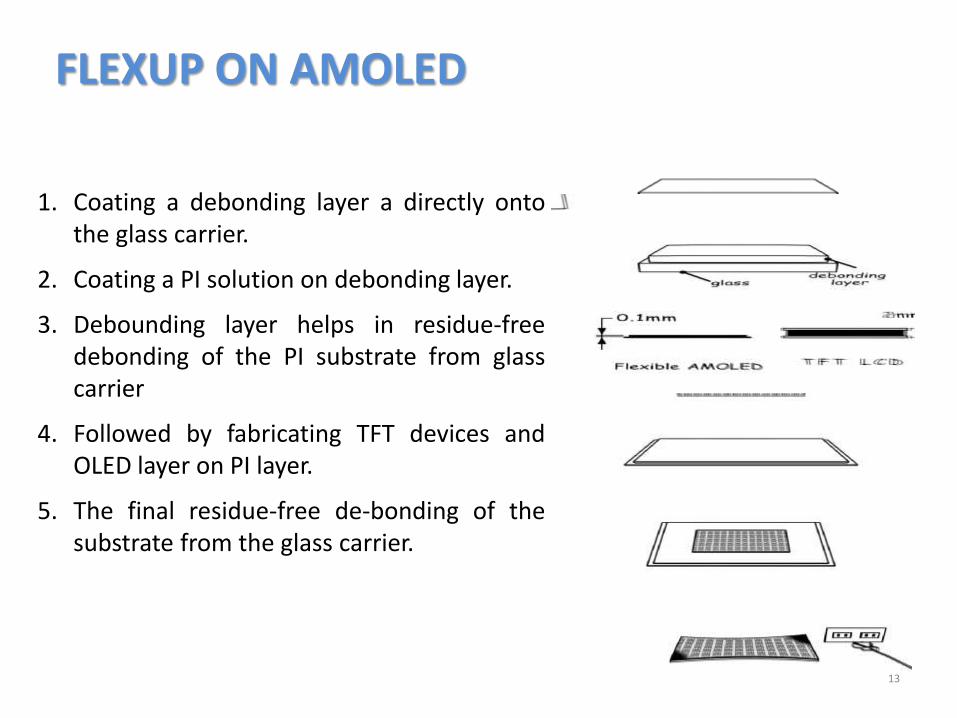
FLEXUP ON AMOLED
13
1. Coating a debonding layer a directly ontothe glass carrier.
2. Coating a PI solution on debonding layer.
3. Debounding layer helps in residue-freedebonding of the PI substrate from glasscarrier
4. Followed by fabricating TFT devices andOLED layer on PI layer.
5. The final residue-free de-bonding of thesubstrate from the glass carrier.
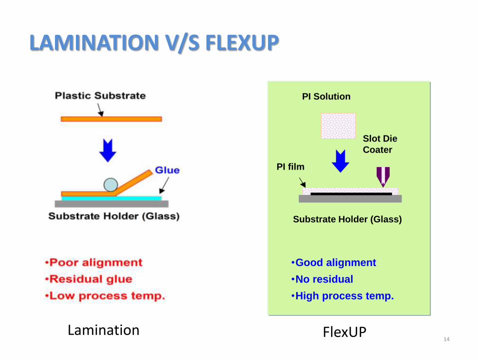
LAMINATION V/S FLEXUP
14
PI Solution
PI film
Substrate Holder (Glass)
Slot Die
Coater
•Good alignment
•No residual
•High process temp.
Lamination FlexUP
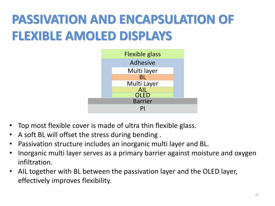
PASSIVATION AND ENCAPSULATION OF FLEXIBLE AMOLED DISPLAYS
15
• Top most flexible cover is made of ultra thin flexible glass. • A soft BL will offset the stress during bending .• Passivation structure includes an inorganic multi layer and BL.• Inorganic multi layer serves as a primary barrier against moisture and oxygen
infiltration. • AIL together with BL between the passivation layer and the OLED layer,
effectively improves flexibility.
PIBarrier
Flexible glass
OLEDAIL
Multi LayerBL
Multi layerAdhesive
TFT BACKPLANE TECHNOLOGIES FOR FLEXUP
16
• Low-temperature poly-Si TFTs and IGZO TFTs are excellent semiconductorsfor OLED driving.
• a-IGZO TFTs are excellent for flexible display, improves the pixel apertureratio and also reduce cost.
• The Back Channel Etching type a-IGZO TFTs were fabricated on a FlexUPsubstrate by using a four-mask process with a process temperature lessthan 300°C.
• The a-IGZO TFT backplane was bent at a 25 mm radius up to 10000 times,with the leakage current maintained below 10–11A.
• Flexible transparent a-IGZO TFTs have the advantages of good electricalcharacteristics and low process temperature.
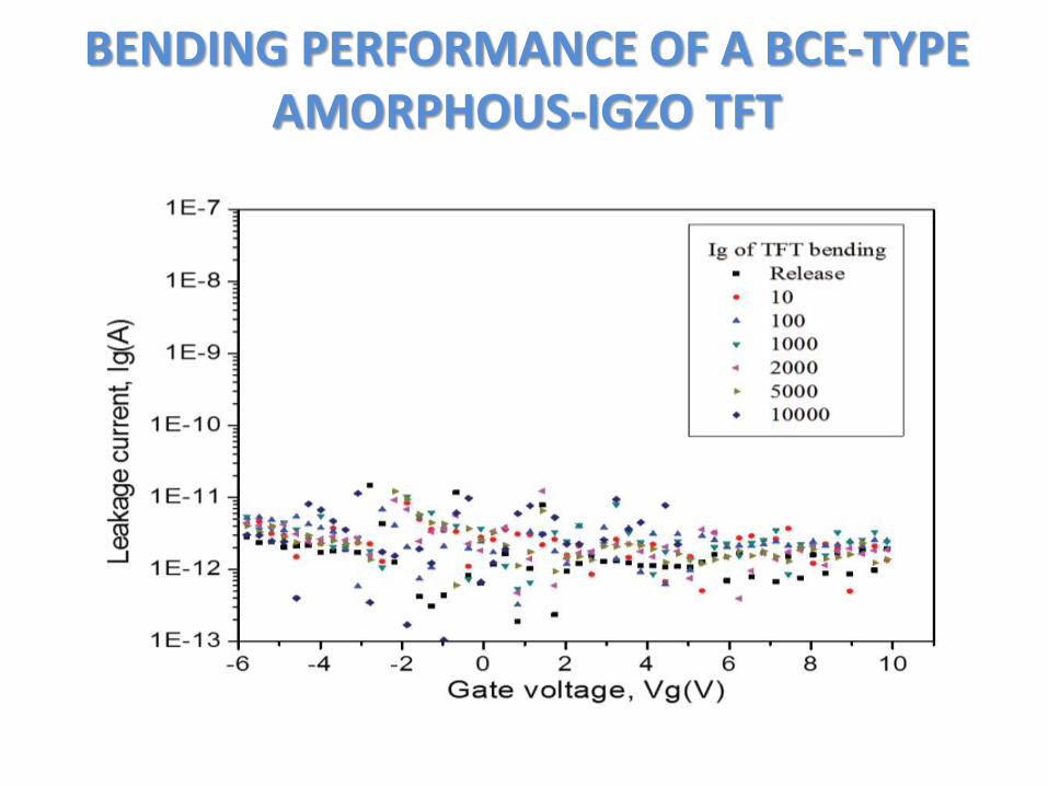
BENDING PERFORMANCE OF A BCE-TYPE AMORPHOUS-IGZO TFT
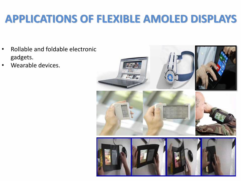
APPLICATIONS OF FLEXIBLE AMOLED DISPLAYS
18
• Rollable and foldable electronic gadgets.
• Wearable devices.
ELECTRONIC PAPER : i2R E-PAPER
• Display technology designed to mimic the appearance of ordinary paper.
• It provides a rewritable, reusable and environmentally friendly print medium - an "electronic paper" - to reduce traditional paper consumption.
• Capable of holding text and images indefinitely without drawing energy, while allowing the image to be changed later
Key features :Wide viewing angleReflects light like ordinary paper Image retain without powerExtremely thin Low manufacturing cost
19
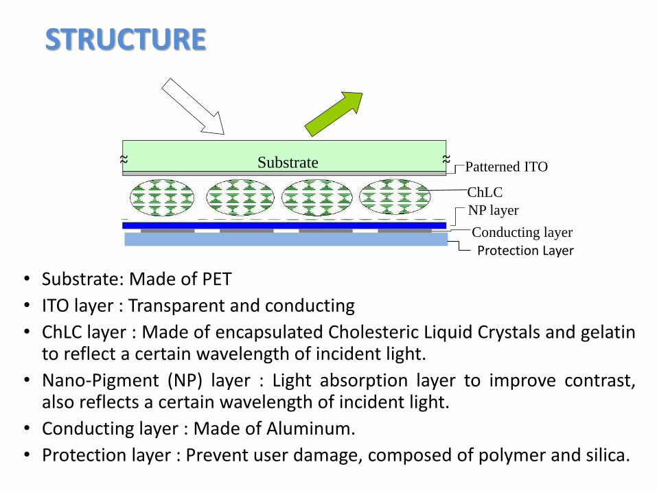
STRUCTURE
• Substrate: Made of PET
• ITO layer : Transparent and conducting
• ChLC layer : Made of encapsulated Cholesteric Liquid Crystals and gelatinto reflect a certain wavelength of incident light.
• Nano-Pigment (NP) layer : Light absorption layer to improve contrast,also reflects a certain wavelength of incident light.
• Conducting layer : Made of Aluminum.
• Protection layer : Prevent user damage, composed of polymer and silica.
Substrate Patterned ITO
ChLC
NP layer
Conducting layer
~~ ~~
Protection Layer
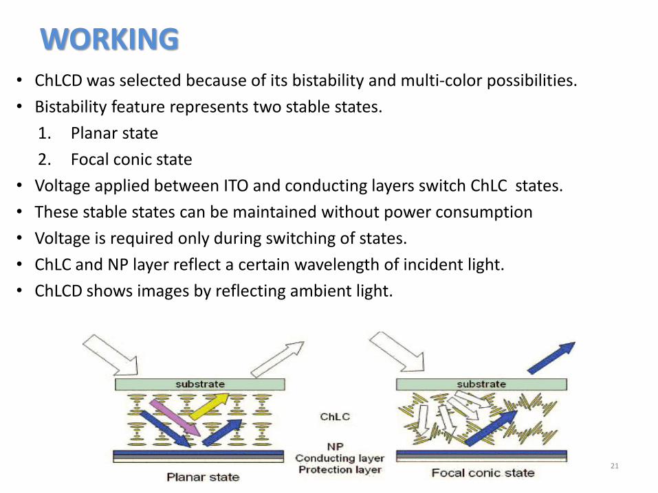
WORKING• ChLCD was selected because of its bistability and multi-color possibilities.
• Bistability feature represents two stable states.
1. Planar state
2. Focal conic state
• Voltage applied between ITO and conducting layers switch ChLC states.
• These stable states can be maintained without power consumption
• Voltage is required only during switching of states.
• ChLC and NP layer reflect a certain wavelength of incident light.
• ChLCD shows images by reflecting ambient light.
21
E-PAPER PRINTING
22
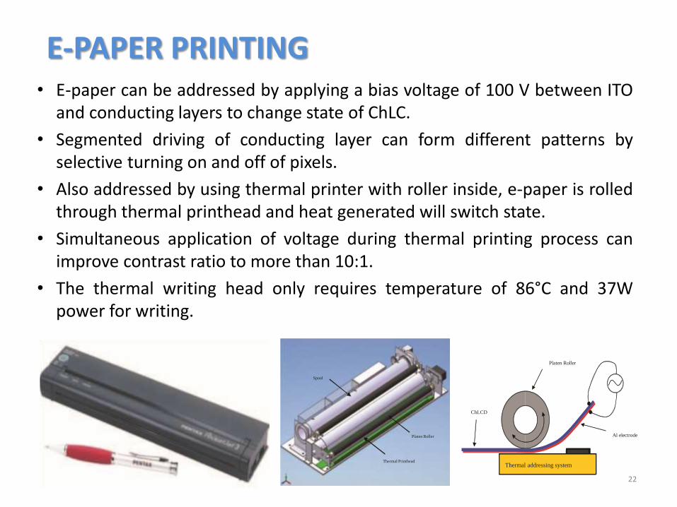
• E-paper can be addressed by applying a bias voltage of 100 V between ITOand conducting layers to change state of ChLC.
• Segmented driving of conducting layer can form different patterns byselective turning on and off of pixels.
• Also addressed by using thermal printer with roller inside, e-paper is rolledthrough thermal printhead and heat generated will switch state.
• Simultaneous application of voltage during thermal printing process canimprove contrast ratio to more than 10:1.
• The thermal writing head only requires temperature of 86°C and 37Wpower for writing.
Thermal Printhead
Platen Roller
Spool
Thermal addressing system
Al electrode
Platen Roller
ChLCD
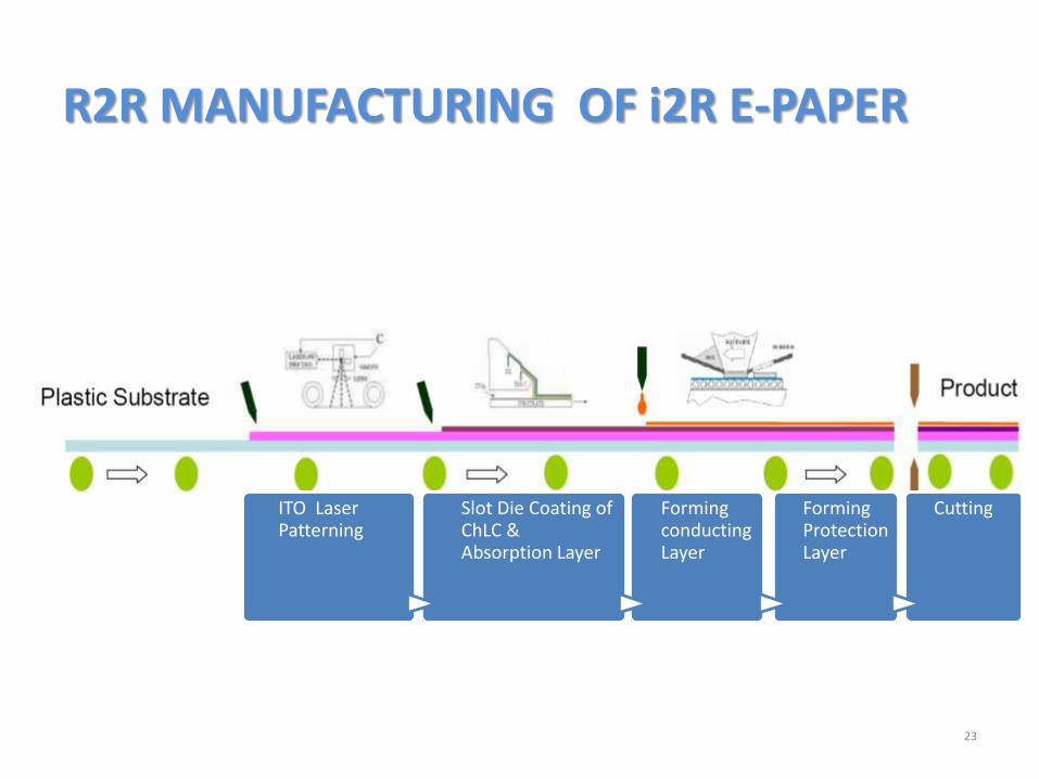
R2R MANUFACTURING OF i2R E-PAPER
23
ITO Laser Patterning
Slot Die Coating of ChLC & Absorption Layer
Forming conducting Layer
Forming Protection Layer
Cutting
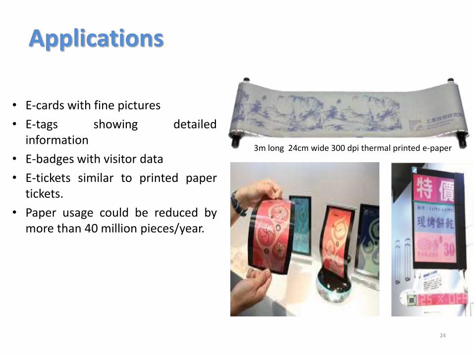
Applications
24
3m long 24cm wide 300 dpi thermal printed e-paper
• E-cards with fine pictures
• E-tags showing detailedinformation
• E-badges with visitor data
• E-tickets similar to printed papertickets.
• Paper usage could be reduced bymore than 40 million pieces/year.
CONCLUSION
25
• We reported a novel technology, the FlexUP, to fabricate AMOLEDdisplays on current glass carrier production line.
• By inserting a release layer, displays and electronic devices are easilyfabricated on substrates and thereafter debonded.
• Presented barrier encapsulation technologies for protecting flexibleAMOLEDs from stress, oxygen and moisture infusion.
• Also attained flexible cheap and rewritable e-paper technology usingR2R production technology.
THANK YOU
26