
Flexible Stainless Steel Substrates for Vehicle Displays · PDF fileFlexible Stainless Steel...
27
1 Flexible Stainless Steel Substrates for Displays V. Cannella, M. Izu, and S. Jones Energy Conversion Devices S. Wagner and I-C. Cheng Princeton University
Transcript of Flexible Stainless Steel Substrates for Vehicle Displays · PDF fileFlexible Stainless Steel...

1
Flexible Stainless Steel Substrates for Displays
V. Cannella, M. Izu, and S. Jones Energy Conversion Devices
S. Wagner and I-C. ChengPrinceton University

2
Background
Substantial recent efforts to develop flexible displays and microelectronics
various military displayswearable displays, direct view screens, curved dashboard displays, rollaway displays
Heavy focus on plastic substratesPET, polycarbonate (PC), PEN, and polyimide (Kapton)Thin, light, flexible, transparent, conformable,Roll-to-roll processing compatible
3
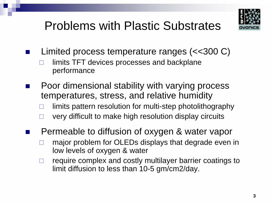
Problems with Plastic Substrates
Limited process temperature ranges (<<300 C) limits TFT devices processes and backplane performance
Poor dimensional stability with varying process temperatures, stress, and relative humidity
limits pattern resolution for multi-step photolithographyvery difficult to make high resolution display circuits
Permeable to diffusion of oxygen & water vapor major problem for OLEDs displays that degrade even in low levels of oxygen & waterrequire complex and costly multilayer barrier coatings to limit diffusion to less than 10-5 gm/cm2/day.

4
Attractive Alternative -Stainless Steel Substrates
For flexible emissive or reflective displays where transparency is not required
Stainless Steel (SS) <5 mils thick, 125 µmprovides a durable flexible substrate tolerates high temperature processesmuch better dimensional stability than plasticperfect diffusion barrier to oxygen & water vaporproven device compatibilityroll-to-roll manufacturing compatibility

5
Stainless Steel SubstratesStable up to 1000 °C
Allow high quality a-Si and gate insulator (>300 °C )Allow growth of large grain poly-Si (500-900 °C)
Perfect Diffusion BarrierImpermeable to oxygen or water vapor
Not degraded by UV, ozone or organic solvents Dimensional stability much better than plastic
Much higher elastic modulusLower coefficient of thermal expansionZero coefficient of hydrolytic expansionNegligible mechanical hysteresisAllows excellent multi-photostep microprocessing
resolutions comparable to Corning 1737 glassResistant to curling due to stress in films
a problem that needs special control with plastic

6
Comparison of SS & Flexible Other Substrates
Thickness (µm) 100 100 100
Weight g/m2) 800 120 220
Safe bending radius (cm) 4 4 40
RTR processable? yes likely unlikely
Visually transparent? no some yes
Max process temp (ºC) 1000 180, 300 600
TCE (ppm/ºC) 10 16 5
Elastic Modulus (GPa) 200 5 70Permeable O2, H2O? no yes no
Coeff Hydrolytic Exp (ppm/%RH) none 11, 11 none
Pre-bake required? no yes maybe
Planarization necessary? yes maybe no
Buffer layer necessary? yes yes maybe
Electrical conductivity high none none
Thermal conductivity (W/m·ºC) 16 0.1-0.2 1Plastic encapsulation substrate thickness for TFTs in neutral plane 8x 1x 5xDeform after device fabrication no yes no
PropertyStainless-
Steel GlassPlastics
(PEN, PI)
7
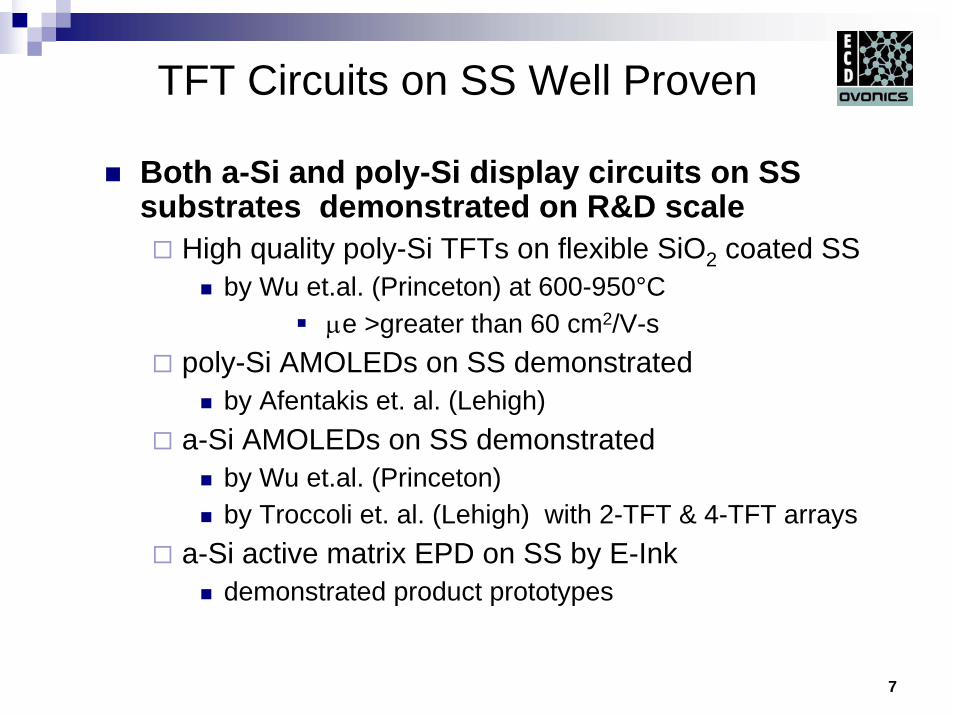
TFT Circuits on SS Well Proven
Both a-Si and poly-Si display circuits on SS substrates demonstrated on R&D scale
High quality poly-Si TFTs on flexible SiO2 coated SSby Wu et.al. (Princeton) at 600-950°C
µe >greater than 60 cm2/V-spoly-Si AMOLEDs on SS demonstrated
by Afentakis et. al. (Lehigh)a-Si AMOLEDs on SS demonstrated
by Wu et.al. (Princeton)by Troccoli et. al. (Lehigh) with 2-TFT & 4-TFT arrays
a-Si active matrix EPD on SS by E-Inkdemonstrated product prototypes

8
Flexible Large-scale SS Substrates in Semiconductor Manufacturing
SS well established as semiconductor substrateLarge area photovoltaic (PV) modules - up to 16 ft2
Both a-Si & CIGS (Copper Indium Gallium Diselenide)
United-Solar Ovonic photovoltaic products on flexible stainless steel
5-mil flexible SS substrate forPV semiconductor devices
9
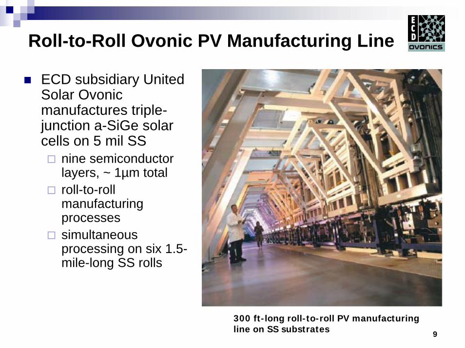
Roll-to-Roll Ovonic PV Manufacturing Line
ECD subsidiary United Solar Ovonicmanufactures triple-junction a-SiGe solar cells on 5 mil SS
nine semiconductor layers, ~ 1µm totalroll-to-roll manufacturing processessimultaneous processing on six 1.5-mile-long SS rolls
300 ft-long roll-to-roll PV manufacturing line on SS substrates

10
Program Scope
Initial development phase for flexible SS substrates
Integrate ECD SS substrate expertise with work at Princeton to planarize, passivate SS, build TFTsDevelop processes for 6” x 6” substrates Characterize substrates Demonstrate a-Si TFT compatibilityProvide sample substrates to USDC team to verify compatibility with OLED and a-Si backplanes
Anticipated follow-up – Scale up to larger areasProcesses compatible with roll-to-roll processing

11
Specific SS Substrate Issues - Planarization
Vendor A Sample 500X Vendor B Sample 500X
Bare SS substrates have rougher surfaces than glass or plasticSS foils come with rolling mill marks that have sharp profiles
can cause device degradation or failureSteel foils must either be polished or planarized with a film
for production we planarize with a spin-on-glass-type layer
12
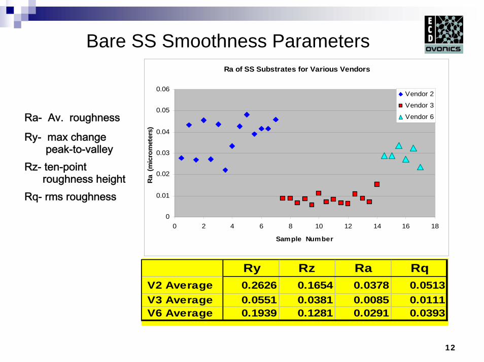
Bare SS Smoothness Parameters Ra of SS Substrates for Various Vendors
0
0.01
0.02
0.03
0.04
0.05
0.06
0 2 4 6 8 10 12 14 16 18
Sample Number
Ra
(mic
rom
eter
s)
Vendor 2
Vendor 3
Vendor 6
Ry Rz Ra Rq V2 Average 0.2626 0.1654 0.0378 0.0513 V3 Average 0.0551 0.0381 0.0085 0.0111 V6 Average 0.1939 0.1281 0.0291 0.0393
Ra- Av. roughness
Ry- max change peak-to-valley
Rz- ten-point roughness height
Rq- rms roughness
13
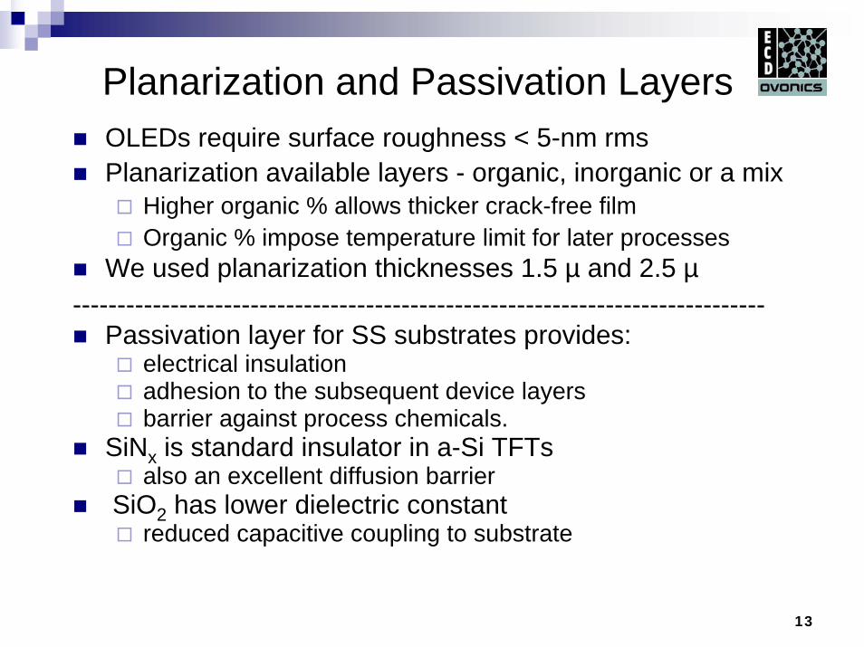
Planarization and Passivation LayersOLEDs require surface roughness < 5-nm rmsPlanarization available layers - organic, inorganic or a mix
Higher organic % allows thicker crack-free filmOrganic % impose temperature limit for later processes
We used planarization thicknesses 1.5 µ and 2.5 µ------------------------------------------------------------------------------
Passivation layer for SS substrates provides:electrical insulation adhesion to the subsequent device layers barrier against process chemicals.
SiNx is standard insulator in a-Si TFTsalso an excellent diffusion barrier
SiO2 has lower dielectric constantreduced capacitive coupling to substrate

14
Schematic cross section (not to scale) of a passivated back-channel a-Si TFT and three
substrates types: (a) glass, (b) plastic,(c) stainless steel
substrate
n+ a-Si:H
Cr
SiNx
i a-Si:HSiNx
(c) stainless steel
passivation planarization
(a) glass
passivation
(b) plastic
passivation
passivation
Specific SS Issues – Electrical Isolation
SS substrates are electrically conductive:
must be coated to provide excellent electrical insulationvideo scan rates require low capacitive coupling of device to substrate
These requirements can be met by combining :
planarization layer followed by electrically insulating capping layer

15
Planarization & Passivation Materials for Various Subsequent Processes
Subsequent Device Process
methyl siloxane silicatespin-on-
glassspin-on-
glasslow temperature process <250°C √ √ √ > 0.2 µm > 0.2 µm
conventional a-Si:H TFT <400°C √ √ > 0.2 µm > 0.2 µm
conventional poly-Si TFT process
>450°C √ > 0.2 µm
laser-annealing √ √ √ > 0.2 µm*
Planarization Layer Passivation Layer
organic polymer
deposited SiO2
deposited SiNx

16
Planarized & Passivated SS Substrate Type A
Without metal With metal

17
Planarized & Passivated SS Substrate Type B
Without metal With metal

18
050603-03 (1.5 µm + SiOx + Mo) 050603-12 (2.5 µm + SiOx + Mo)
Typical Inclusion Defects

19
SS Substrate Sample SmoothnessSample Planarization
ThicknessSiOx Mo Slide # Graph TypMag. X-res. Y-res. Baseline ∆h ∆h (peak)
050603-03 1.5 µm 200 nm N/A 5 optical low
(no Mo region) 6 optical high7 profilometry 0.4 µm 10 µm √ < 100 nm8 profilometry ~ 273 nm
050603-03 1.5 µm 200 nm 100 nm 10 optical low
(Mo region) 11 optical high12 profilometry 0.4 µm 10 µm √ < 80 nm13 profilometry ~ 51 nm14 profilometry ~ 193 nm15 profilometry 2 µm ~ 212 nm
050603-12 2.5 µm 200 nm N/A 18 optical low
(no Mo region) 19 optical high20 profilometry 0.4 µm 10 µm √ < 40 nm21 profilometry 2 µm ~ 38 nm
050603-12 2.5 µm 200 nm 100 23 optical low
(Mo region) nm 24 optical high25 optical high26 profilometry 0.4 µm 10 µm √ < 35 nm27 profilometry ~ 63 nm28 profilometry ~ 69 nm29 profilometry ~ 1030 nm30 profilometry 2 µm ~ 60 nm

20
SS Substrate Smoothness SummaryOptical micrograph of sample without Mo:
looks rough but actual surface is smoothimage reflects the surface roughness of the steel substratedifficult to locate the defects (image interfered by the substrate roughness)
Baseline area surface is very smooth surface roughness (peak-to-peak) over 300 µm square:
050603-03 (w/ Mo) 1.5 µm < 80 nmRa (AFM) ~ 5 -10 nm
050603-12 (w/ Mo) 2.5 µm < 35 nmRa (AFM) < 5 nm
Defect types:050603-03 1.5 µm point defects050603-12 2.5 µm point defects & line defects

21
Electrical Isolation
050603_04 Formatted Map 050603_05 Formatted Map 050603_06 Formatted Map
5.1E+07 5.1E+07 5.1E+07 5.1E+07 5.1E+07 5.1E+07 5.1E+07 5.1E+07 5.1E+07 5.1E+07 5.1E+07 5.1E+07 5.1E+07 5.1E+07 676195 5.1E+07 5.1E+07 5.1E+07 5.1E+07 5.1E+07 5.1E+07 5.1E+07 5.1E+07 5.1E+07 5.1E+07 5.1E+07 5.1E+07 5.1E+07 5.1E+07 5.1E+07 5.1E+07 5.1E+07 5.1E+07 5.1E+07 5.1E+07 5.1E+07
5.1E+07 5.1E+07 5.1E+07 5.1E+07 5.1E+07 5.1E+07 5.1E+07 5.1E+07 5.1E+07 5.1E+07 5.1E+07 5.1E+07 5.1E+07 5.1E+07 5.1E+07 5.1E+07 5.1E+07 5.1E+07 5.1E+07 5.1E+07 5.1E+07 5.1E+07 5.1E+07 5.1E+07 5.1E+07 5.1E+07 5.1E+07 5.1E+07 5.1E+07 5.1E+07 5.1E+07 5.1E+07 5.1E+07 5.1E+07 5.1E+07 5.1E+07
1.7E+07 5.1E+07 5.1E+07 5.1E+07 5.1E+07 5.1E+07 5.1E+07 5.1E+07 5.1E+07 5.1E+07 5.1E+07 5.1E+07 5.1E+07 5.1E+07 5.1E+07 5.1E+07 5.1E+07 5.1E+07 5.1E+07 5.1E+07 5.1E+07 5.1E+07 5.1E+07 5.1E+07 5.1E+07 5.1E+07 5.1E+07 5.1E+07 5.1E+07 5.1E+07 5.1E+07 5.1E+07 5.1E+07 5.1E+07 5.1E+07 5.1E+07
5.1E+07 5.1E+07 5.1E+07 5.1E+07 5.1E+07 5.1E+07 5.1E+07 5.1E+07 5.1E+07 5.1E+07 5.1E+07 5.1E+07 5.1E+07 5.1E+07 5.1E+07 5.1E+07 5.1E+07 5.1E+07 5.1E+07 5.1E+07 5.1E+07 5.1E+07 5.1E+07 5.1E+07 5.1E+07 5.1E+07 5.1E+07 5.1E+07 5.1E+07 5.1E+07 5.1E+07 5.1E+07 5.1E+07 5.1E+07 5.1E+07 5.1E+07
5.1E+07 5.1E+07 5.1E+07 5.1E+07 5.1E+07 5.1E+07 5.1E+07 5.1E+07 5.1E+07 5.1E+07 5.1E+07 5.1E+07 5.1E+07 5.1E+07 5.1E+07 5.1E+07 5.1E+07 5.1E+07 5.1E+07 5.1E+07 5.1E+07 5.1E+07 5.1E+07 5.1E+07 5.1E+07 5.1E+07 5.1E+07 5.1E+07 5.1E+07 5.1E+07 5.1E+07 5.1E+07 5.1E+07 5.1E+07 5.1E+07 5.1E+07
5.1E+07 5.1E+07 5.1E+07 5.1E+07 5.1E+07 5.1E+07 5.1E+07 5.1E+07 5.1E+07 5.1E+07 5.1E+07 5.1E+07 5.1E+07 5.1E+07 5.1E+07 5.1E+07 5.1E+07 5.1E+07 5.1E+07 5.1E+07 5.1E+07 5.1E+07 5.1E+07 5.1E+07 5.1E+07 5.1E+07 5.1E+07 5.1E+07 5.1E+07 5.1E+07 5.1E+07 5.1E+07 5.1E+07 5.1E+07 5.1E+07 5.1E+07
5.1E+07 5.1E+07 5.1E+07 5.1E+07 5.1E+07 5.1E+07 5.1E+07 5.1E+07 5.1E+07 5.1E+07 5.1E+07 397955 5.1E+07 5.1E+07 5.1E+07 5.1E+07 5.1E+07 5.1E+07 5.1E+07 5.1E+07 5.1E+07 5.1E+07 5.1E+07 5.1E+07 5.1E+07 5.1E+07 5.1E+07 5.1E+07 5.1E+07 5.1E+07 5.1E+07 5.1E+07 5.1E+07 5.1E+07 5.1E+07 5.1E+07
5.1E+07 5.1E+07 5.1E+07 5.1E+07 5.1E+07 5.1E+07 5.1E+07 5.1E+07 5.1E+07 5.1E+07 5.1E+07 5.1E+07 5.1E+07 5.1E+07 5.1E+07 5.1E+07 5.1E+07 5.1E+07 5.1E+07 5.1E+07 5.1E+07 5.1E+07 5.1E+07 5.1E+07 5.1E+07 5.1E+07 5.1E+07 5.1E+07 5.1E+07 5.1E+07 5.1E+07 5.1E+07 5.1E+07 5.1E+07 5.1E+07 5.1E+07
5.1E+07 5.1E+07 5.1E+07 5.1E+07 5.1E+07 5.1E+07 5.1E+07 5.1E+07 5.1E+07 5.1E+07 5.1E+07 5.1E+07 5.1E+07 5.1E+07 5.1E+07 5.1E+07 5.1E+07 5.1E+07 5.1E+07 5.1E+07 5.1E+07 5.1E+07 5.1E+07 5.1E+07 5.1E+07 5.1E+07 5.1E+07 5.1E+07 5.1E+07 5.1E+07 5.1E+07 5.1E+07 5.1E+07 5.1E+07 5.1E+07 5.1E+07
5.1E+07 5.1E+07 5.1E+07 5.1E+07 5.1E+07 5.1E+07 5.1E+07 5.1E+07 5.1E+07 5.1E+07 5.1E+07 5.1E+07 5.1E+07 5.1E+07 5.1E+07 5.1E+07 5.1E+07 5.1E+07 5.1E+07 5.1E+07 5.1E+07 5.1E+07 5.1E+07 5.1E+07 5.1E+07 5.1E+07 5.1E+07 5.1E+07 5.1E+07 5.1E+07 5.1E+07 5.1E+07 5.1E+07 5.1E+07 5.1E+07 5.1E+07
1E+07 5.1E+07 5.1E+07 5.1E+07 5.1E+07 5.1E+07 5.1E+07 5.1E+07 5.1E+07 5.1E+07 5.1E+07 5.1E+07 5.1E+07 5.1E+07 5.1E+07 5.1E+07 5.1E+07 5.1E+07 5.1E+07 5.1E+07 5.1E+07 5.1E+07 5.1E+07 5.1E+07 5.1E+07 5.1E+07 5.1E+07 5.1E+07 5.1E+07 5.1E+07 5.1E+07 5.1E+07 5.1E+07 5.1E+07 5.1E+07 5.1E+07
5.1E+07 5.1E+07 5.1E+07 5.1E+07 5.1E+07 5.1E+07 5.1E+07 5.1E+07 5.1E+07 5.1E+07 5.1E+07 5.1E+07 5.1E+07 5.1E+07 5.1E+07 5.1E+07 5.1E+07 5.1E+07 5.1E+07 5.1E+07 5.1E+07 5.1E+07 5.1E+07 5.1E+07 5.1E+07 5.1E+07 5.1E+07 5.1E+07 5.1E+07 5.1E+07 5.1E+07 5.1E+07 5.1E+07 5.1E+07 5.1E+07 5.1E+07
050603_07 Formatted Map 050603_08 Formatted Map 050603_09 Formatted Map
5.1E+07 5.1E+07 5.1E+07 5.1E+07 5.1E+07 5.1E+07 5.1E+07 5.1E+07 5.1E+07 5.1E+07 5.1E+07 5.1E+07 5.1E+07 5.1E+07 5.1E+07 5.1E+07 5.1E+07 5.1E+07 5.1E+07 5.1E+07 5.1E+07 5.1E+07 5.1E+07 5.1E+07 5.1E+07 5.1E+07 5.1E+07 5.1E+07 5.1E+07 5.1E+07 5.1E+07 5.1E+07 5.1E+07 5.1E+07 5.1E+07 5.1E+07
5.1E+07 5.1E+07 5.1E+07 5.1E+07 5.1E+07 5.1E+07 5.1E+07 5.1E+07 5.1E+07 5.1E+07 5.1E+07 5.1E+07 5.1E+07 5.1E+07 5.1E+07 5.1E+07 5.1E+07 5.1E+07 5.1E+07 5.1E+07 5.1E+07 5.1E+07 5.1E+07 5.1E+07 5.1E+07 5.1E+07 5.1E+07 5.1E+07 5.1E+07 5.1E+07 5.1E+07 5.1E+07 5.1E+07 1.3E+07 5.1E+07 5.1E+07
5.1E+07 5.1E+07 5.1E+07 5.1E+07 5.1E+07 5.1E+07 5.1E+07 5.1E+07 5.1E+07 5.1E+07 5.1E+07 5.1E+07 5.1E+07 5.1E+07 5.1E+07 5.1E+07 5.1E+07 5.1E+07 5.1E+07 5.1E+07 5.1E+07 5.1E+07 5.1E+07 5.1E+07 5.1E+07 5.1E+07 5.1E+07 5.1E+07 5.1E+07 5.1E+07 5.1E+07 5.1E+07 5.1E+07 5.1E+07 5.1E+07 5.1E+07
5.1E+07 5.1E+07 5.1E+07 5.1E+07 5.1E+07 5.1E+07 5.1E+07 5.1E+07 5.1E+07 5.1E+07 5.1E+07 5.1E+07 5.1E+07 5.1E+07 5.1E+07 5.1E+07 5.1E+07 5.1E+07 5.1E+07 5.1E+07 5.1E+07 5.1E+07 5.1E+07 5.1E+07 5720048 5.1E+07 5.1E+07 5.1E+07 5.1E+07 5.1E+07 5.1E+07 5.1E+07 5.1E+07 5.1E+07 5.1E+07 5.1E+07
5.1E+07 5.1E+07 5.1E+07 5.1E+07 5.1E+07 5.1E+07 5.1E+07 5.1E+07 5.1E+07 5.1E+07 5.1E+07 5.1E+07 5.1E+07 5.1E+07 5.1E+07 5.1E+07 5.1E+07 5.1E+07 5.1E+07 5.1E+07 5.1E+07 5.1E+07 5.1E+07 5.1E+07 5.1E+07 5.1E+07 5.1E+07 5.1E+07 5.1E+07 5.1E+07 5.1E+07 285024 2.6E+07 5.1E+07 5.1E+07 5.1E+07
5.1E+07 5.1E+07 5.1E+07 5.1E+07 5.1E+07 5.1E+07 5.1E+07 5.1E+07 5.1E+07 5.1E+07 5.1E+07 5.1E+07 5.1E+07 5.1E+07 5.1E+07 5.1E+07 5.1E+07 5.1E+07 5.1E+07 5.1E+07 5.1E+07 5.1E+07 5.1E+07 5.1E+07 5.1E+07 5.1E+07 5.1E+07 5.1E+07 5.1E+07 5.1E+07 5.1E+07 5.1E+07 5.1E+07 5.1E+07 5.1E+07 2.6E+07
5.1E+07 5.1E+07 5.1E+07 5.1E+07 5.1E+07 5.1E+07 5.1E+07 5.1E+07 5.1E+07 5.1E+07 5147940 5.1E+07 5.1E+07 5.1E+07 5.1E+07 5.1E+07 5.1E+07 5.1E+07 5.1E+07 5.1E+07 5.1E+07 5.1E+07 5.1E+07 5.1E+07 2.6E+07 2.6E+07 2.6E+07 2.6E+07 2.6E+07 2.6E+07 2.6E+07 2.6E+07 2.6E+07 2.6E+07 1.7E+07 1.3E+07
5.1E+07 5.1E+07 5.1E+07 5.1E+07 5.1E+07 5.1E+07 5.1E+07 5.1E+07 5.1E+07 5.1E+07 5.1E+07 5.1E+07 5.1E+07 5.1E+07 5.1E+07 5.1E+07 5.1E+07 5.1E+07 5.1E+07 5.1E+07 5.1E+07 5.1E+07 5.1E+07 5.1E+07 1.3E+07 1.3E+07 1.3E+07 1.3E+07 1.3E+07 1.3E+07 1.3E+07 1.3E+07 1.3E+07 1E+07 1.3E+07 1.3E+07
5.1E+07 5.1E+07 5.1E+07 5.1E+07 5.1E+07 5.1E+07 5.1E+07 5.1E+07 5.1E+07 5.1E+07 5.1E+07 5.1E+07 5.1E+07 5.1E+07 5.1E+07 5.1E+07 5.1E+07 5.1E+07 5.1E+07 5.1E+07 5.1E+07 5.1E+07 5.1E+07 5.1E+07 1E+07 1.3E+07 1E+07 1E+07 1E+07 8580587 1E+07 1E+07 1E+07 1E+07 1E+07 1E+07
5.1E+07 5.1E+07 5.1E+07 5.1E+07 5.1E+07 5.1E+07 5.1E+07 5.1E+07 5.1E+07 5.1E+07 5.1E+07 5.1E+07 5.1E+07 5.1E+07 5.1E+07 5.1E+07 5.1E+07 5.1E+07 5.1E+07 5.1E+07 5.1E+07 5.1E+07 5.1E+07 5.1E+07 1.3E+07 1E+07 1.3E+07 1E+07 1E+07 1.3E+07 1E+07 1E+07 1E+07 1E+07 1E+07 1E+07
5.1E+07 5.1E+07 5.1E+07 5.1E+07 5.1E+07 5.1E+07 5.1E+07 5.1E+07 5.1E+07 5.1E+07 5.1E+07 5.1E+07 5.1E+07 5.1E+07 5.1E+07 5.1E+07 5.1E+07 5.1E+07 5.1E+07 5.1E+07 5.1E+07 5.1E+07 5.1E+07 5.1E+07 1E+07 1E+07 3959716 1E+07 8580587 1E+07 1E+07 1E+07 1E+07 1E+07 1E+07 1E+07
5.1E+07 5.1E+07 5.1E+07 5.1E+07 5.1E+07 5.1E+07 5.1E+07 5.1E+07 5.1E+07 5.1E+07 5.1E+07 5.1E+07 5.1E+07 5.1E+07 5.1E+07 5.1E+07 5.1E+07 5.1E+07 5.1E+07 5.1E+07 5.1E+07 5.1E+07 5.1E+07 5.1E+07 1E+07 1E+07 1E+07 1E+07 1.7E+07 1.7E+07 1.7E+07 1.7E+07 1.7E+07 1.7E+07 1.7E+07 1.7E+07
Electrical Resistance measurements on 3mm x 3mm MIM squares
Green=high resistance, Yellow=partial shunting, Red=short

22
pF 1 2 3 4 5 6 7 8 9 10 11 12 13 14 15 161 246
2 226
3 221
4 221
5 225 221 222 217 222
6 218 214 212 208 215
7 221
8 222 220
9 255 226 231 241 218 222 221 222 220 215 213 220 221 222 223 230
10 218
11 223 220 219 214 217
12 226 224 222 212 214
13 235
14 222
15 221
16 284 284 288
Capacitance (pF) of 3mm x 3mm MIM squaresSample 050603-07 2.5µ Planarization

23
TFT Compatibility
To verify TFT compatibility we fabricated common gate TFT structures SS substrates proved compatible with all a-Si processes
300 C processes for a-Si, Si3N4, SiO2, plasma etching, etc.
Substrate planarity compatible with 4 µm photopatterningOnly one common gate device out of 20 showed shuntingEastman Kodak Company and Princeton University also collaborated to fabricate a-Si TFTs on these stainless steel substrates
device performance was similar to TFTs made on glass

24
Commercial Availability & EconomicsSS foil is currently available commercially with a surface finish compatible with planarization layers at <$10/m2
< equivalent polyimide, ~ same as high quality PENProduction planarization will use high utilization coating processes (not “spin-on”)SS substrates need only one PECVD insulator coatMaterials cost for planarization & passivation ~ $20/m2
Planarized passivated SS substrates will be economically attractive vs. plastic substrates
Plastic substrates for OLEDs require multilayer barrier coatings estimated to cost >$50/m2

25
Outlook for Flexible SS SubstratesPlanarized & passivated SS substrates can provide functional substrates for flexible electronics & displaysSS is attractive vs. plastics for flexible displays:
thermal stability compatible with both a-Si & poly-Si TFTsexcellent mechanical stability for multi-photostep processingperfect barrier against diffusion of O2 & H2O more rugged and robust than plastics, suited to applications that require mechanical strength, flexibility, & resiliencechemical stability to organic solvents, to UV radiation, and ozone
Active matrix circuits on SS substrates are provenboth a-Si and high-temperature poly-Si TFTs
Planarized passivated SS will be economically very attractive compared to plastic with barrier layers
26
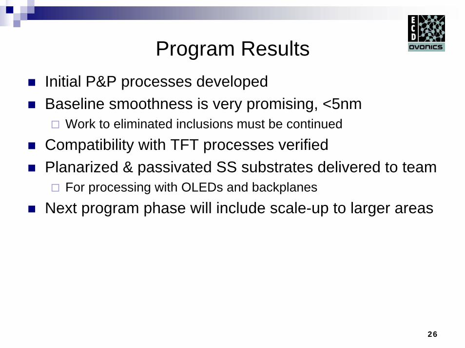
Program ResultsInitial P&P processes developedBaseline smoothness is very promising, <5nm
Work to eliminated inclusions must be continued
Compatibility with TFT processes verifiedPlanarized & passivated SS substrates delivered to team
For processing with OLEDs and backplanes
Next program phase will include scale-up to larger areas

27
Acknowledgements
USDC and ARL for partial funding of this workDave Beglau and Bud Dotter who did all the hands-on work for this program


![Welcome [] · lighting, TFTs and display circuits on flexible substrates, vehicle displays and user interface technology trends, and wearable displays. With a three day exhibition](https://static.fdocuments.in/doc/165x107/5f5cef5a1e32812432314750/welcome-lighting-tfts-and-display-circuits-on-flexible-substrates-vehicle.jpg)