Technical Data Rev. 4, 3/2009 RF Power Field Effect Transistors · MRF6VP41KHR6 MRF6VP41KHSR6 5 RF...
18
RF Power Field Effect Transistors N- Channel Enhancement- Mode Lateral MOSFETs Designed primarily for pulsed wideband applications with frequencies up to 500 MHz. Devices are unmatched and are suitable for use in industrial, medical and scientific applications. • Typical Pulsed Performance at 450 MHz: V DD = 50 Volts, I DQ = 150 mA, P out = 1000 Watts Peak (200 W Avg.), Pulse Width = 100 μsec, Duty Cycle = 20% Power Gain 20 dB Drain Efficiency 64% • Capable of Handling 10:1 VSWR, @ 50 Vdc, 450 MHz, 1000 Watts Peak Power Features • CW Operation Capability with Adequate Liquid Cooling • Qualified Up to a Maximum of 50 V DD Operation • Integrated ESD Protection • Excellent Thermal Stability • Designed for Push - Pull Operation • Greater Negative Gate-Source Voltage Range for Improved Class C Operation • RoHS Compliant • In Tape and Reel. R6 Suffix = 150 Units per 56 mm, 13 inch Reel. Table 1. Maximum Ratings Rating Symbol Value Unit Drain-Source Voltage V DSS -0.5, +110 Vdc Gate-Source Voltage V GS - 6, +10 Vdc Storage Temperature Range T stg - 65 to +150 °C Case Operating Temperature T C 150 °C Operating Junction Temperature T J 200 °C CW Operation @ T C = 25°C Derate above 25°C CW 1107 4.6 W W/°C Document Number: MRF6VP41KH Rev. 4, 3/2009 Freescale Semiconductor Technical Data MRF6VP41KHR6 MRF6VP41KHSR6 10 -500 MHz, 1000 W, 50 V LATERAL N-CHANNEL BROADBAND RF POWER MOSFETs CASE 375D - 05, STYLE 1 NI-1230 MRF6VP41KHR6 PARTS ARE PUSH-PULL (Top View) RF outA /V DSA 3 1 4 2 RF outB /V DSB RF inA /V GSA RF inB /V GSB Figure 1. Pin Connections CASE 375E - 04, STYLE 1 NI - 1230S MRF6VP41KHSR6 © Freescale Semiconductor, Inc., 2008 - 2009. All rights reserved.
-
Upload
truongtuyen -
Category
Documents
-
view
225 -
download
0
Transcript of Technical Data Rev. 4, 3/2009 RF Power Field Effect Transistors · MRF6VP41KHR6 MRF6VP41KHSR6 5 RF...

MRF6VP41KHR6 MRF6VP41KHSR6
1RF Device DataFreescale Semiconductor
RF Power Field Effect TransistorsN-Channel Enhancement-Mode Lateral MOSFETs
Designed primarily for pulsed wideband applications with frequencies up to500 MHz. Devices are unmatched and are suitable for use in industrial,medical and scientific applications.
• Typical Pulsed Performance at 450 MHz: VDD = 50 Volts, IDQ = 150 mA, Pout = 1000 Watts Peak (200 W Avg.), Pulse Width = 100 μsec,Duty Cycle = 20%
Power Gain � 20 dBDrain Efficiency � 64%
• Capable of Handling 10:1 VSWR, @ 50 Vdc, 450 MHz, 1000 Watts PeakPower
Features• CW Operation Capability with Adequate Liquid Cooling• Qualified Up to a Maximum of 50 VDD Operation• Integrated ESD Protection• Excellent Thermal Stability• Designed for Push-Pull Operation• Greater Negative Gate-Source Voltage Range for Improved Class C
Operation• RoHS Compliant• In Tape and Reel. R6 Suffix = 150 Units per 56 mm, 13 inch Reel.
Table 1. Maximum Ratings
Rating Symbol Value Unit
Drain-Source Voltage VDSS -0.5, +110 Vdc
Gate-Source Voltage VGS -6, +10 Vdc
Storage Temperature Range Tstg - 65 to +150 °C
Case Operating Temperature TC 150 °C
Operating Junction Temperature TJ 200 °C
CW Operation @ TC = 25°CDerate above 25°C
CW 11074.6
WW/°C
Document Number: MRF6VP41KHRev. 4, 3/2009
Freescale SemiconductorTechnical Data
MRF6VP41KHR6MRF6VP41KHSR6
10-500 MHz, 1000 W, 50 VLATERAL N-CHANNEL
BROADBANDRF POWER MOSFETs
CASE 375D-05, STYLE 1NI-1230
MRF6VP41KHR6
PARTS ARE PUSH-PULL
(Top View)
RFoutA/VDSA3 1
4 2 RFoutB/VDSB
RFinA/VGSA
RFinB/VGSB
Figure 1. Pin Connections
CASE 375E-04, STYLE 1NI-1230S
MRF6VP41KHSR6
© Freescale Semiconductor, Inc., 2008-2009. All rights reserved.
2RF Device Data
Freescale Semiconductor
MRF6VP41KHR6 MRF6VP41KHSR6
Table 2. Thermal Characteristics
Characteristic Symbol Value (1,2) Unit
Thermal Resistance, Junction to CaseCase Temperature 80°C, 1000 W Pulsed, 100 μsec Pulse Width, 20% Duty Cycle, 450 MHzCase Temperature 48°C, 1000 W CW, 352.2 MHz
RθJC0.030.15
°C/W
Table 3. ESD Protection Characteristics
Test Methodology Class
Human Body Model (per JESD22-A114) 2 (Minimum)
Machine Model (per EIA/JESD22-A115) A (Minimum)
Charge Device Model (per JESD22-C101) IV (Minimum)
Table 4. Electrical Characteristics (TC = 25°C unless otherwise noted)
Characteristic Symbol Min Typ Max Unit
Off Characteristics (3)
Gate-Source Leakage Current(VGS = 5 Vdc, VDS = 0 Vdc)
IGSS � � 10 μAdc
Drain-Source Breakdown Voltage(ID = 300 mA, VGS = 0 Vdc)
V(BR)DSS 110 � � Vdc
Zero Gate Voltage Drain Leakage Current(VDS = 50 Vdc, VGS = 0 Vdc)
IDSS � � 100 μAdc
Zero Gate Voltage Drain Leakage Current(VDS = 100 Vdc, VGS = 0 Vdc)
IDSS � � 5 mA
On Characteristics
Gate Threshold Voltage (3)
(VDS = 10 Vdc, ID = 1600 μAdc)VGS(th) 1 1.68 3 Vdc
Gate Quiescent Voltage (4)
(VDD = 50 Vdc, ID = 150 mAdc, Measured in Functional Test)VGS(Q) 1.5 2.2 3.5 Vdc
Drain-Source On-Voltage (3)
(VGS = 10 Vdc, ID = 4 Adc)VDS(on) � 0.28 � Vdc
Dynamic Characteristics (3)
Reverse Transfer Capacitance(VDS = 50 Vdc ± 30 mV(rms)ac @ 1 MHz, VGS = 0 Vdc)
Crss � 3.3 � pF
Output Capacitance(VDS = 50 Vdc ± 30 mV(rms)ac @ 1 MHz, VGS = 0 Vdc)
Coss � 147 � pF
Input Capacitance(VDS = 50 Vdc, VGS = 0 Vdc ± 30 mV(rms)ac @ 1 MHz)
Ciss � 506 � pF
Functional Tests (4) (In Freescale Test Fixture, 50 ohm system) VDD = 50 Vdc, IDQ = 150 mA, Pout = 1000 W Peak (200 W Avg.), f = 450 MHz,100 μsec Pulse Width, 20% Duty Cycle
Power Gain Gps 19 20 22 dB
Drain Efficiency ηD 60 64 � %
Input Return Loss IRL � -18 -9 dB
1. MTTF calculator available at http://www.freescale.com/rf. Select Software & Tools/Development Tools/Calculators to access MTTFcalculators by product.
2. Refer to AN1955, Thermal Measurement Methodology of RF Power Amplifiers. Go to http://www.freescale.com/rf. Select Documentation/Application Notes - AN1955.
3. Each side of device measured separately.4. Measurement made with device in push-pull configuration.
(continued)

MRF6VP41KHR6 MRF6VP41KHSR6
3RF Device DataFreescale Semiconductor
Table 4. Electrical Characteristics (TC = 25°C unless otherwise noted) (continued)
Characteristic Symbol Min Typ Max Unit
Typical Performance � 352.2 MHz (In Freescale 352.2 MHz Test Fixture, 50 ohm system) VDD = 50 Vdc, IDQ = 150 mA, Pout = 1000 W CW
Power Gain Gps � 20.1 � dB
Drain Efficiency ηD � 67 � %
Input Return Loss IRL � -10.2 � dB
Typical Performance � 500 MHz (In Freescale 500 MHz Test Fixture, 50 ohm system) VDD = 50 Vdc, IDQ = 150 mA, Pout = 1000 W Peak(200 W Avg.), f = 500 MHz, 100 μsec Pulse Width, 20% Duty Cycle
Power Gain Gps � 19.5 � dB
Drain Efficiency ηD � 66 � %
Input Return Loss IRL � -23 � dB

4RF Device Data
Freescale Semiconductor
MRF6VP41KHR6 MRF6VP41KHSR6
Figure 2. MRF6VP41KHR6(HSR6) Test Circuit Schematic � 450 MHz
Z14*, Z15* 0.764″ x 0.150″ MicrostripZ16, Z17 0.290″ x 0.430″ MicrostripZ18, Z19 0.100″ x 0.430″ MicrostripZ20, Z21, Z22, Z23 0.080″ x 0.430″ MicrostripZ24 0.257″ x 0.215″ MicrostripPCB Arlon CuClad 250GX-0300-55-22, 0.030″, εr = 2.55
* Line length includes microstrip bends
Z1 0.366″ x 0.082″ MicrostripZ2*, Z3* 0.170″ x 0.100″ MicrostripZ4*, Z5* 0.220″ x 0.451″ MicrostripZ6, Z7 0.117″ x 0.726″ MicrostripZ8*, Z9* 0.792″ x 0.058″ MicrostripZ10, Z11 0.316″ x 0.726″ MicrostripZ12, Z13 0.262″ x 0.507″ Microstrip
RF
INPUT
Z4
C5
Z5
C6
Z1
DUT
VSUPPLY
Z13
RF
OUTPUTZ24
VBIAS
Z9
Z2
Z3
Z15
Z14
B1
C22
C24
Z18 Z20
C25 C28 C29
+
COAX1
COAX2
COAX3
COAX4
Z22
C1
+
L1
C7 C8
Z6
Z7
C23
C21
C20
C19
Z23
C18
Z21
C17
Z19
C16C9 C10
Z10
Z11
L2
B2
C11
+
C13C12 C14
Z8
C3C2 C4
Z12 Z16
Z17
C15
C26 C27 C30
+VBIAS
VSUPPLY
C31 C34 C35
+
C32 C33 C36
+
L3
L4
Table 5. MRF6VP41KHR6(HSR6) Test Circuit Component Designations and Values � 450 MHzPart Description Part Number Manufacturer
B1, B2 47 Ω, 100 MHz Short Ferrite Beads 2743019447 Fair -Rite
C1, C11 47 μF, 50 V Electrolytic Capacitors 476KXM063M Illinois
C2, C12, C28, C34 0.1 μF Chip Capacitors CDR33BX104AKYS Kemet
C3, C13, C27, C33 220 nF, 50 V Chip Capacitors C1812C224K5RAC Kemet
C4, C14 2.2 μF, 50 V Chip Capacitors C1825C225J5RAC Kemet
C5, C6, C8, C15 27 pF Chip Capacitors ATC100B270JT500XT ATC
C7, C10 0.8-8.0 pF Variable Capacitors 27291SL Johanson Components
C9 33 pF Chip Capacitor ATC100B330JT500XT ATC
C16 12 pF Chip Capacitor ATC100B120JT500XT ATC
C17 10 pF Chip Capacitor ATC100B100JT500XT ATC
C18 9.1 pF Chip Capacitor ATC100B9R1CT500XT ATC
C19 8.2 pF Chip Capacitor ATC100B8R2CT500XT ATC
C20, C21, C22, C23,C25, C32
240 pF Chip Capacitors ATC100B241JT200XT ATC
C24 5.6 pF Chip Capacitor ATC100B5R6CT500XT ATC
C26, C31 2.2 μF, 100 V Chip Capacitors 2225X7R225KT3AB ATC
C29, C30, C35, C36 330 μF, 63 V Electrolytic Capacitors EMVY630GTR331MMH0S Nippon Chemi-Con
Coax1, 2, 3. 4 25 Ω Semi Rigid Coax, 2.2″ Long UT-141C-25 Micro-Coax
L1, L2 2.5 nH, 1 Turn Inductors A01TKLC Coilcraft
L3, L4 43 nH, 10 Turn Inductors B10TJLC Coilcraft

MRF6VP41KHR6 MRF6VP41KHSR6
5RF Device DataFreescale Semiconductor
Figure 3. MRF6VP41KHR6(HSR6) Test Circuit Component Layout � 450 MHz
CU
T O
UT
AR
EA
MRF6VP41KH
Rev. 1
COAX1
C1
B1 C2 C3C4
L1
C5
C6
COAX2
C7
C8 C9
C10
C11
B2 C12
C13
C14 C33
C34
C36C35
C31C32
L4
COAX3
COAX4
C15
C16
C17
C19C18
C24
C22C23
C21
C20
L3
C25 C26
C27
C28
C29
C30
L2

6RF Device Data
Freescale Semiconductor
MRF6VP41KHR6 MRF6VP41KHSR6
TYPICAL CHARACTERISTICS
50
1
1000
0 2010
VDS, DRAIN−SOURCE VOLTAGE (VOLTS)
Figure 4. Capacitance versus Drain-Source Voltage
C, C
AP
AC
ITA
NC
E (
pF)
30
Ciss
100
10
40
Coss
Crss
Measured with ±30 mV(rms)ac @ 1 MHz
VGS = 0 Vdc
1
100
1
TC = 25°C
10
10
VDS, DRAIN−SOURCE VOLTAGE (VOLTS)
Figure 5. DC Safe Operating Area
I D,
DR
AIN
CU
RR
EN
T (
AM
PS
)
100
TJ = 200°C
TJ = 175°C
TJ = 150°C
Note: Each side of device measured separately.
21
1
0
80
10
18
16
14
70
60
50
40
30
Pout, OUTPUT POWER (WATTS) PULSED
Figure 6. Pulsed Power Gain and Drain Efficiencyversus Output Power
Gps
, PO
WE
R G
AIN
(dB
)
η D, D
RA
IN E
FF
ICIE
NC
Y (
%)
ηD
17
15
13
1000 2000
Gps
20
19
20
100
10
VDD = 50 Vdc
IDQ = 150 mA
f = 450 MHz
Pulse Width = 100 μsec
Duty Cycle = 20%
55
65
34
63
62
61
Pin, INPUT POWER (dBm) PULSED
Figure 7. Pulsed Output Power versusInput Power
64
60
44
59
58
57
35 36 37 38 39 40 41 42
Pou
t, O
UT
PU
T P
OW
ER
(dB
m)
P3dB = 60.70 dBm (1174.89 W)
Actual
Ideal
P1dB = 60.33 dBm (1078.94 W)
56
43
VDD = 50 Vdc
IDQ = 150 mA
f = 450 MHz
Pulse Width = 100 μsec
Duty Cycle = 20%
17
23
10
20
19
Pout, OUTPUT POWER (WATTS) PULSED
Figure 8. Pulsed Power Gain versusOutput Power
Gps
, PO
WE
R G
AIN
(dB
)
100
18
IDQ = 6000 mA
1000 2000
3600 mA
1500 mA
150 mA
375 mA
750 mA
21
22
VDD = 50 Vdc
f = 450 MHz
Pulse Width = 100 μsec
Duty Cycle = 20%
Figure 9. Pulsed Power Gain versusOutput Power
Pout, OUTPUT POWER (WATTS) PULSED
Gps
, PO
WE
R G
AIN
(dB
)
VDD = 30 V
12
22
0
1635 V
20
45 V
200 400 600 800 1000 1200 1400
50 V
40 V
14
18
IDQ = 150 Vdc, f = 450 MHz
Pulse Width = 100 μsec
Duty Cycle = 20%
Note: Each side of device measured separately.

MRF6VP41KHR6 MRF6VP41KHSR6
7RF Device DataFreescale Semiconductor
TYPICAL CHARACTERISTICS
45
35
65
20
25�C
TC = −30�C
85�C
3525
55
50
Pin, INPUT POWER (dBm) PULSED
Figure 10. Pulsed Output Power versusInput Power
Pou
t, O
UT
PU
T P
OW
ER
(dB
m)
30 40
60
45
40
VDD = 50 Vdc
IDQ = 150 mA
f = 450 MHz
Pulse Width = 100 μsec
Duty Cycle = 20%
22
1
0
100
100
17
15
13
70
60
50
40
30
Pout, OUTPUT POWER (WATTS) PULSED
Figure 11. Pulsed Power Gain and Drain Efficiencyversus Output Power
Gps
, PO
WE
R G
AIN
(dB
)
η D, D
RA
IN E
FF
ICIE
NC
Y (
%)
ηD16
14
12
1000 2000
25�C
TC = −30�C
85�C
20
18
Gps
19
20
21
10
80
90
10
VDD = 50 Vdc
IDQ = 150 mA
f = 450 MHz
Pulse Width = 100 μsec
Duty Cycle = 20%
0.2
1 10
RECTANGULAR PULSE WIDTH (S)
Figure 12. Maximum Transient Thermal Impedance
ZJC
, T
HE
RM
AL
IMP
ED
AN
CE
(°C
/W)
0.00001
D = 0.7
0.18
0.16
0.14
0.12
0.1
0.08
0.06
0.04
0.02
0
0.0001 0.001 0.01 0.1
D = 0.5
D = 0.1D = Duty Factor = t1/t2t1 = Pulse Widtht2 = Pulse PeriodTJ = PD * ZJC + TC
t2
t1PD
250
109
90
TJ, JUNCTION TEMPERATURE (°C)
Figure 13. MTTF versus Junction Temperature � Pulsed
This above graph displays calculated MTTF in hours when the device
is operated at VDD = 50 Vdc, Pout = 1000 W Peak, Pulse Width = 100 μsec,
Duty Cycle = 20%, and ηD = 64%.
MTTF calculator available at http://www.freescale.com/rf. Select
Software & Tools/Development Tools/Calculators to access MTTF
calculators by product.
108
107
106
110 130 150 170 190
MT
TF
(H
OU
RS
)
210 230 250
109
90
TJ, JUNCTION TEMPERATURE (°C)
Figure 14. MTTF versus Junction Temperature � CW
This above graph displays calculated MTTF in hours when the device
is operated at VDD = 50 Vdc, Pout = 1000 W CW, and ηD = 67%.
MTTF calculator available at http://www.freescale.com/rf. Select
Software & Tools/Development Tools/Calculators to access MTTF
calculators by product.
108
107
105
110 130 150 170 190
MT
TF
(H
OU
RS
)
210 230
106
8RF Device Data
Freescale Semiconductor
MRF6VP41KHR6 MRF6VP41KHSR6
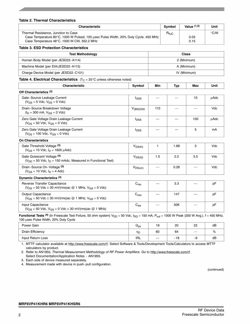
Zo = 2 Ω
Zload
f = 450 MHz
Zsourcef = 450 MHz
VDD = 50 Vdc, IDQ = 150 mA, Pout = 1000 W Peak
fMHz
Zsource�
Zload�
450 0.86 + j1.06 1.58 + j1.22
Zsource = Test circuit impedance as measured from gate to gate, balanced configuration.
Zload = Test circuit impedance as measured from drain to drain, balanced configuration.
Figure 15. Series Equivalent Source and Load Impedance � 450 MHz
Zsource
Zload
Input
Matching
Network
Device
Under
Test
Output
Matching
Network
−
− +
+

MRF6VP41KHR6 MRF6VP41KHSR6
9RF Device DataFreescale Semiconductor
Figure 16. MRF6VP41KHR6(HSR6) Test Circuit Component Layout � 352.2 MHz
--
CU
T O
UT
AR
EA
MRF6VP41KH352 MHz
Rev. 1
C11C9 C7
C5
L1
C1
C2
C3
C4
L2
C12B2 C10
C8
C6
L4
C21 C23
C20 C22
C13
L3
C14
C17C16
C15
C18
C19
COAX1
COAX2
COAX3
COAX4
Table 6. MRF6VP41KHR6(HSR6) Test Circuit Component Designations and Values � 352.2 MHzPart Description Part Number Manufacturer
B1, B2 47 Ω, 100 MHz Short Ferrite Beads 2743019447 Fair -Rite
Coax1, 2, 3, 4 25 Ω Semi Rigid coax, 2.2″ Long UT141-25 Precision Tube Company
C1, C2 27 pF Chip Capacitors ATC100B270JT500XT ATC
C3 0.8-8.0 pF Variable Capacitor, Gigatrim 27291SL Johanson
C4 75 pF Chip Capacitor ATC100B750JT500XT ATC
C5, C6 2.2 μF Chip Capacitors C1825C225J5RAC Kemet
C7, C8 220 nF Chip Capacitors C1812C224J5RAC Kemet
C9, C10 0.1 μF Chip Capacitors CDR33BX104AKYS AVX
C11, C12 47 μF, 50 V Electrolytic Capacitors 476KXM050M Illinois Cap
C13 36 pF 500 V Chip Capacitor MCM01-009ED360J-F CDE
C14, C15, C16, C17 240 pF Chip Capacitors ATC100B241JT200XT ATC
C18, C19 2.2 μF Chip Capacitors G2225X7R225KT3AB ATC
C20, C21, C22, C23 470 μF, 63 V Electrolytic Capacitors MCRH63V477M13X21-RH Multicomp
L1, L2 2.5 nH Inductors A01T Coilcraft
L3, L4 10 Turn #16 AWG ID=0.160″ Inductors, Hand Wound Copper Wire Freescale
PCB Arlon CuClad 250GX-0300-55-22, 0.030″, εr = 2.55 DS2655 DS Electronics

10RF Device Data
Freescale Semiconductor
MRF6VP41KHR6 MRF6VP41KHSR6
Zo = 10 Ω Zload
f = 352.2 MHz
Zsource
f = 352.2 MHz
VDD = 50 Vdc, IDQ = 150 mA, Pout = 1000 W CW
fMHz
Zsource�
Zload�
352.2 0.5 + j6.5 2.9 + j6.35
Zsource = Test circuit impedance as measured from gate to gate, balanced configuration.
Zload = Test circuit impedance as measured from drain to drain, balanced configuration.
Figure 17. Series Equivalent Source and Load Impedance � 352.2 MHz
Zsource
Zload
Input
Matching
Network
Device
Under
Test
Output
Matching
Network
−
− +
+

MRF6VP41KHR6 MRF6VP41KHSR6
11RF Device DataFreescale Semiconductor
Figure 18. MRF6VP41KHR6(HSR6) Test Circuit Component Layout � 500 MHz
CU
T O
UT
AR
EA
MRF6VP41KH
Rev. 1
COAX1
C1
B1 C2 C3C4
L1
C5
C6
COAX2
C7
C8 C9
C10
C11
B2 C12
C13
C14 C33
C34
C36C35
C31C32
L4
COAX3
COAX4
C15
C16
C19C18
C24
C22C23
C21
C20
L3
C25 C26
C27
C28
C29
C30
L2
C17 not used in MRF6VP41KHR6(HSR6) 500 MHz application.
Table 7. MRF6VP41KHR6(HSR6) Test Circuit Component Designations and Values � 500 MHzPart Description Part Number Manufacturer
B1, B2 47 Ω, 100 MHz Short Ferrite Beads 2743019447 Fair -Rite
Coax1, 2, 3, 4 25 Ω Semi Rigid coax, 2.2″ Long UT-141C-25 Micro-Coax
C1, C11 47 μF, 50 V Electrolytic Capacitors 476KXM063M Illinois
C2, C12, C28, C34 0.1 μF Chip Capacitors CDR33BX104AKYS Kemet
C3, C13, C27, C33 220 nF, 50 V Chip Capacitors C1812C224K5RAC Kemet
C4, C14 2.2 μF, 50 V Chip Capacitors C1825C225J5RAC Kemet
C5, C6, C15 27 pF Chip Capacitors ATC100B270JT500XT ATC
C7, C10 0.8-8.0 pF Variable Capacitors 27291SL Johanson Components
C9 33 pF Chip Capacitor ATC100B330JT500XT ATC
C8 13 pF Chip Capacitor ATC100B120JT500XT ATC
C18 9.1 pF Chip Capacitor ATC100B9R1CT500XT ATC
C19, C16 8.2 pF Chip Capacitors ATC100B8R2CT500XT ATC
C20, C21, C22, C23, C25,C32
240 pF Chip Capacitors ATC100B241JT200XT ATC
C24 5.6 pF Chip Capacitor ATC100B5R6CT500XT ATC
C26, C31 2.2 μF, 100 V Chip Capacitors 2225X7R225KT3AB ATC
C29, C30, C35, C36 330 μF, 63 V Electrolytic Capacitors MCRH63V337M13X21-RH Multicomp
L1, L2 2.5 nH, 1 Turn Inductors A01TKLC Coilcraft
L3, L4 43 nH, 10 Turn Inductors B10TJLC Coilcraft
C17 not used in MRF6VP41KHR6(HSR6) 500 MHz application.

12RF Device Data
Freescale Semiconductor
MRF6VP41KHR6 MRF6VP41KHSR6
Zo = 2 Ω
Zload
f = 500 MHz
Zsource
f = 500 MHz
VDD = 50 Vdc, IDQ = 150 mA, Pout = 1000 W Peak
fMHz
Zsource�
Zload�
500 0.75 + j0.5 1.73 + j0.95
Zsource = Test circuit impedance as measured from gate to gate, balanced configuration.
Zload = Test circuit impedance as measured from drain to drain, balanced configuration.
Figure 19. Series Equivalent Source and Load Impedance � 500 MHz
Zsource
Zload
Input
Matching
Network
Device
Under
Test
Output
Matching
Network
−
− +
+

MRF6VP41KHR6 MRF6VP41KHSR6
13RF Device DataFreescale Semiconductor
PACKAGE DIMENSIONS

14RF Device Data
Freescale Semiconductor
MRF6VP41KHR6 MRF6VP41KHSR6
MRF6VP41KHR6 MRF6VP41KHSR6
15RF Device DataFreescale Semiconductor

16RF Device Data
Freescale Semiconductor
MRF6VP41KHR6 MRF6VP41KHSR6

MRF6VP41KHR6 MRF6VP41KHSR6
17RF Device DataFreescale Semiconductor
PRODUCT DOCUMENTATION
Refer to the following documents to aid your design process.
Application Notes
• AN1955: Thermal Measurement Methodology of RF Power Amplifiers
Engineering Bulletins• EB212: Using Data Sheet Impedances for RF LDMOS Devices
REVISION HISTORY
The following table summarizes revisions to this document.
Revision Date Description
0 Jan. 2008 • Initial Release of Data Sheet
1 Apr. 2008 • Added Fig. 12, Maximum Transient Thermal Impedance, p. 6
2 Sept. 2008 • Added Note to Fig. 4, Capacitance versus Drain-Source Voltage, to denote that each side of device ismeasured separately, p. 5
• Updated Fig. 5, DC Safe Operating Area, to clarify that measurement is on a per-side basis, p. 5
• Corrected Fig. 13, MTTF versus Junction Temperature, to reflect the correct die size and increased theMTTF factor accordingly, p. 6
3 Nov. 2008 • Added CW operation capability bullet to Features section, p. 1
• Added CW operation to Maximum Ratings table, p. 1
• Added CW thermal data to Thermal Characteristics table, p. 2
• Fig. 14, Series Equivalent Source and Load Impedance, corrected Zsource copy to read �Test circuitimpedance as measured from gate to gate, balanced configuration� and Zload copy to read �Test circuitimpedance as measured from drain to drain, balanced configuration�; replaced impedance diagram to showpush-pull test conditions, p. 7
4 Mar. 2009 • CW rating limits updated from 1176 W to 1107 W and 5.5 W/°C to 4.6 W/°C to reflect recent remeasureddata, Max Ratings table, p. 1
• CW Thermal Characteristics changed from 81°C to 48°C and 0.16 °C/W to 0.15 °C/W using data from themost recent 352.2 MHz CW application circuit, p. 2
• Added Typical Performances table for 352.2 MHz and 500 MHz applications, p. 3
• Added Fig. 14, MTTF versus Junction Temperature - CW, p. 7
• Added Figs. 16 and 18, Test Circuit Component Layout - 352.2 MHz and 500 MHz, and Tables 6 and 7, TestCircuit Component Designations and Values - 352.2 MHz and 500 MHz, p. 9, 11
• Added Figs. 17 and 19, Series Equivalent Source and Load Impedance - 352.2 MHz and 500 MHz, p. 10, 12
18RF Device Data
Freescale Semiconductor
MRF6VP41KHR6 MRF6VP41KHSR6
Information in this document is provided solely to enable system and softwareimplementers to use Freescale Semiconductor products. There are no express orimplied copyright licenses granted hereunder to design or fabricate any integratedcircuits or integrated circuits based on the information in this document.
Freescale Semiconductor reserves the right to make changes without further notice toany products herein. Freescale Semiconductor makes no warranty, representation orguarantee regarding the suitability of its products for any particular purpose, nor doesFreescale Semiconductor assume any liability arising out of the application or use ofany product or circuit, and specifically disclaims any and all liability, including withoutlimitation consequential or incidental damages. �Typical� parameters that may beprovided in Freescale Semiconductor data sheets and/or specifications can and dovary in different applications and actual performance may vary over time. All operatingparameters, including �Typicals�, must be validated for each customer application bycustomer�s technical experts. Freescale Semiconductor does not convey any licenseunder its patent rights nor the rights of others. Freescale Semiconductor products arenot designed, intended, or authorized for use as components in systems intended forsurgical implant into the body, or other applications intended to support or sustain life,or for any other application in which the failure of the Freescale Semiconductor productcould create a situation where personal injury or death may occur. Should Buyerpurchase or use Freescale Semiconductor products for any such unintended orunauthorized application, Buyer shall indemnify and hold Freescale Semiconductorand its officers, employees, subsidiaries, affiliates, and distributors harmless against allclaims, costs, damages, and expenses, and reasonable attorney fees arising out of,directly or indirectly, any claim of personal injury or death associated with suchunintended or unauthorized use, even if such claim alleges that FreescaleSemiconductor was negligent regarding the design or manufacture of the part.
Freescale� and the Freescale logo are trademarks of Freescale Semiconductor, Inc.All other product or service names are the property of their respective owners.© Freescale Semiconductor, Inc. 2008-2009. All rights reserved.
How to Reach Us:
Home Page:www.freescale.com
Web Support:http://www.freescale.com/support
USA/Europe or Locations Not Listed:Freescale Semiconductor, Inc.Technical Information Center, EL5162100 East Elliot RoadTempe, Arizona 852841-800-521-6274 or +1-480-768-2130www.freescale.com/support
Europe, Middle East, and Africa:Freescale Halbleiter Deutschland GmbHTechnical Information CenterSchatzbogen 781829 Muenchen, Germany+44 1296 380 456 (English)+46 8 52200080 (English)+49 89 92103 559 (German)+33 1 69 35 48 48 (French)www.freescale.com/support
Japan:Freescale Semiconductor Japan Ltd.HeadquartersARCO Tower 15F1-8-1, Shimo-Meguro, Meguro-ku,Tokyo 153-0064Japan0120 191014 or +81 3 5437 [email protected]
Asia/Pacific:Freescale Semiconductor China Ltd.Exchange Building 23FNo. 118 Jianguo RoadChaoyang DistrictBeijing 100022 China +86 10 5879 [email protected]
For Literature Requests Only:Freescale Semiconductor Literature Distribution CenterP.O. Box 5405Denver, Colorado 802171-800-441-2447 or +1-303-675-2140Fax: [email protected]
Document Number: MRF6VP41KHRev. 4, 3/2009