System Organization Chapter Three
62
Page 83 System Organization Chapter Three To write even a modest 80x86 assembly language program requires considerable familiarity with the 80x86 family. To write good assembly language programs requires a strong knowledge of the underlying hardware. Unfortunately, the underlying hardware is not consistent. Techniques that are crucial for 8088 programs may not be useful on 80486 systems. Likewise, programming techniques that provide big performance boosts on an 80486 chip may not help at all on an 80286. Fortunately, some programming techniques work well whatever microprocessor you’re using. This chapter discusses the effect hard- ware has on the performance of computer software. 3.0 Chapter Overview This chapter describes the basic components that make up a computer system: the CPU, memory, I/O, and the bus that connects them. Although you can write software that is ignorant of these concepts, high performance software requires a complete understand- ing of this material. This chapter begins by discussing bus organization and memory organization. These two hardware components will probably have a bigger performance impact on your soft- ware than the CPU’s speed. Understanding the organization of the system bus will allow you to design data structures that operate and maximum speed. Similarly, knowing about memory performance characteristics, data locality, and cache operation can help you design software that runs as fast as possible. Of course, if you’re not interested in writing code that runs as fast as possible, you can skip this discussion; however, most people do care about speed at one point or another, so learning this information is useful. Unfortunately, the 80x86 family microprocessors are a complex group and often over- whelm beginning students. Therefore, this chapter describes four hypothetical members of the 80x86 family: the 886, 8286, the 8486, and the 8686 microprocessors. These represent simplified versions of the 80x86 chips and allow a discussion of various architectural fea- tures without getting bogged down by huge CISC instruction sets. This text uses the x86 hypothetical processors to describe the concepts of instruction encoding, addressing modes, sequential execution, the prefetch queue, pipelining, and superscalar operation. Once again, these are concepts you do not need to learn if you only want to write correct software. However, if you want to write fast software as well, especially on advanced pro- cessors like the 80486, Pentium, and beyond, you will need to learn about these concepts. Some might argue that this chapter gets too involved with computer architecture. They feel such material should appear in an architectural book, not an assembly language programming book. This couldn’t be farther from the truth! Writing good assembly lan- guage programs requires a strong knowledge of the architecture. Hence the emphasis on computer architecture in this chapter. 3.1 The Basic System Components The basic operational design of a computer system is called its architecture. John Von Neumann, a pioneer in computer design, is given credit for the architecture of most com- puters in use today. For example, the 80x86 family uses the Von Neumann architecture (VNA). A typical Von Neumann system has three major components: the central processing unit (or CPU), memory, and input/output (or I/O). The way a system designer combines these components impacts system performance (see Figure 3.1). In VNA machines, like the 80x86 family, the CPU is where all the action takes place. All computations occur inside the CPU. Data and CPU instructions reside in memory until required by the CPU. To the CPU, most I/O devices look like memory because the Thi d t td ith F Mk 402
Transcript of System Organization Chapter Three
Page 83
System Organization Chapter Three
To write even a modest 80x86 assembly language program requires considerablefamiliarity with the 80x86 family. To write
good
assembly language programs requires astrong knowledge of the underlying hardware. Unfortunately, the underlying hardware isnot consistent. Techniques that are crucial for 8088 programs may not be useful on 80486systems. Likewise, programming techniques that provide big performance boosts on an80486 chip may not help at all on an 80286. Fortunately, some programming techniqueswork well whatever microprocessor you’re using. This chapter discusses the effect hard-ware has on the performance of computer software.
3.0 Chapter Overview
This chapter describes the basic components that make up a computer system: theCPU, memory, I/O, and the bus that connects them. Although you can write software thatis ignorant of these concepts, high performance software requires a complete understand-ing of this material.
This chapter begins by discussing bus organization and memory organization. Thesetwo hardware components will probably have a bigger performance impact on your soft-ware than the CPU’s speed. Understanding the organization of the system bus will allowyou to design data structures that operate and maximum speed. Similarly, knowing aboutmemory performance characteristics, data locality, and cache operation can help youdesign software that runs as fast as possible. Of course, if you’re not interested in writingcode that runs as fast as possible, you can skip this discussion; however, most people docare about speed at one point or another, so learning this information is useful.
Unfortunately, the 80x86 family microprocessors are a complex group and often over-whelm beginning students. Therefore, this chapter describes four hypothetical membersof the 80x86 family: the 886, 8286, the 8486, and the 8686 microprocessors. These representsimplified versions of the 80x86 chips and allow a discussion of various architectural fea-tures without getting bogged down by huge CISC instruction sets. This text uses the x86hypothetical processors to describe the concepts of instruction encoding, addressingmodes, sequential execution, the prefetch queue, pipelining, and superscalar operation.Once again, these are concepts you do not need to learn if you only want to write
correct
software. However, if you want to write
fast
software as well, especially on advanced pro-cessors like the 80486, Pentium, and beyond, you will need to learn about these concepts.
Some might argue that this chapter gets too involved with computer architecture.They feel such material should appear in an architectural book, not an assembly languageprogramming book. This couldn’t be farther from the truth! Writing
good
assembly lan-guage programs requires a strong knowledge of the architecture. Hence the emphasis oncomputer architecture in this chapter.
3.1 The Basic System Components
The basic operational design of a computer system is called its
architecture
. John VonNeumann, a pioneer in computer design, is given credit for the architecture of most com-puters in use today. For example, the 80x86 family uses the
Von Neumann
architecture
(VNA). A typical Von Neumann system has three major components: the
central processingunit
(or
CPU
),
memory,
and
input/output
(or
I/O
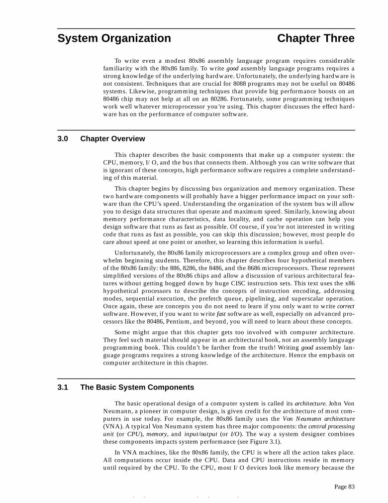
). The way a system designer combinesthese components impacts system performance (see Figure 3.1).
In VNA machines, like the 80x86 family, the CPU is where all the action takes place.All computations occur inside the CPU. Data and CPU instructions reside in memoryuntil required by the CPU. To the CPU, most I/O devices look like memory because the
Thi d t t d ith F M k 4 0 2
Chapter 03
Page 84
CPU can store data to an output device and read data from an input device. The major dif-ference between memory and I/O locations is the fact that I/O locations are generallyassociated with external devices in the outside world.
3.1.1 The System Bus
The
system bus
connects the various components of a VNA machine. The 80x86 familyhas three major busses: the
address
bus, the
data
bus, and the
control
bus. A bus is a collec-tion of wires on which electrical signals pass between components in the system. Thesebusses vary from processor to processor. However, each bus carries comparable informa-tion on all processors; e.g., the data bus may have a different implementation on the 80386than on the 8088, but both carry data between the processor, I/O, and memory.
A typical 80x86 system component uses
standard TTL logic levels.
This means eachwire on a bus uses a standard voltage level to represent zero and one
1
. We will alwaysspecify zero and one rather than the electrical levels because these levels vary on differentprocessors (especially laptops).
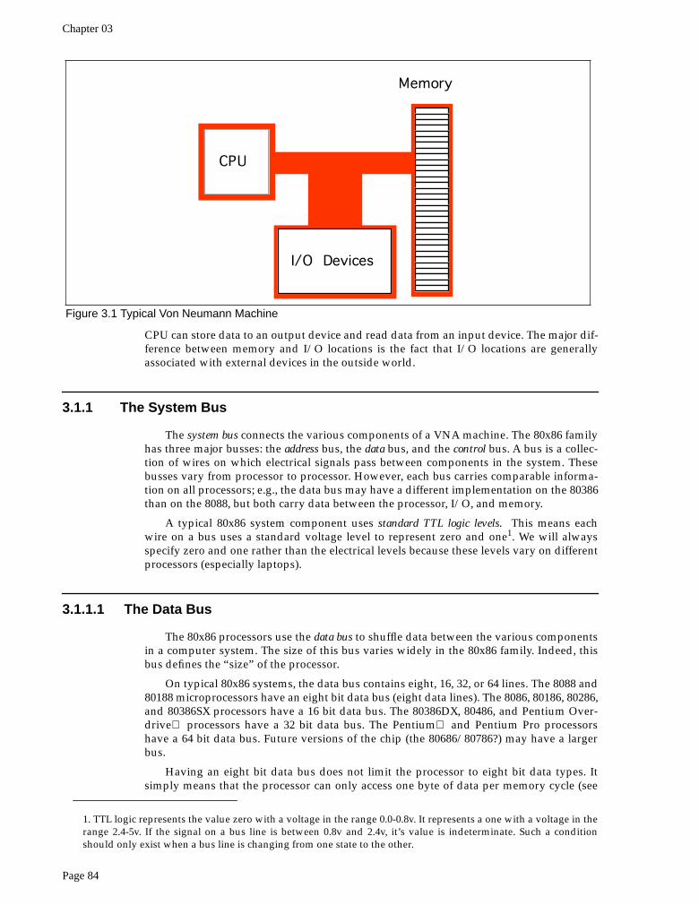
3.1.1.1 The Data Bus
The 80x86 processors use the
data bus
to shuffle data between the various componentsin a computer system. The size of this bus varies widely in the 80x86 family. Indeed, thisbus defines the “size” of the processor.
On typical 80x86 systems, the data bus contains eight, 16, 32, or 64 lines. The 8088 and80188 microprocessors have an eight bit data bus (eight data lines). The 8086, 80186, 80286,and 80386SX processors have a 16 bit data bus. The 80386DX, 80486, and Pentium Over-drive
processors have a 32 bit data bus. The Pentium
and Pentium Pro processorshave a 64 bit data bus. Future versions of the chip (the 80686/80786?) may have a largerbus.
Having an eight bit data bus does not limit the processor to eight bit data types. Itsimply means that the processor can only access one byte of data per memory cycle (see
1. TTL logic represents the value zero with a voltage in the range 0.0-0.8v. It represents a one with a voltage in therange 2.4-5v. If the signal on a bus line is between 0.8v and 2.4v, it’s value is indeterminate. Such a conditionshould only exist when a bus line is changing from one state to the other.
Figure 3.1 Typical Von Neumann Machine
CPU
Memory
I/O Devices
System Organization
Page 85
“The Memory Subsystem” on page 87 for a description of memory cycles). Therefore, theeight bit bus on an 8088 can only transmit half the information per unit time (memorycycle) as the 16 bit bus on the 8086. Therefore, processors with a 16 bit bus are naturallyfaster than processors with an eight bit bus. Likewise, processors with a 32 bit bus arefaster than those with a 16 or eight bit data bus. The size of the data bus affects the perfor-mance of the system more than the size of any other bus.
You’ll often hear a processor called an
eight, 16, 32, or 64 bit processor.
While there is amild controversy concerning the size of a processor, most people now agree that the num-ber of data lines on the processor determines its size. Since the 80x86 family busses areeight, 16, 32, or 64 bits wide, most data accesses are also eight, 16, 32, or 64 bits. Althoughit is possible to process 12 bit data with an 8088, most programmers process 16 bits sincethe processor will fetch and manipulate 16 bits anyway. This is because the processoralways fetches eight bits. To fetch 12 bits requires two eight bit memory operations. Sincethe processor fetches 16 bits rather than 12, most programmers use all 16 bits. In general,manipulating data which is eight, 16, 32, or 64 bits in length is the most efficient.
Although the 16, 32, and 64 bit members of the 80x86 family
can
process data up to thewidth of the bus, they can also access smaller memory units of eight, 16, or 32 bits. There-fore, anything you can do with a small data bus can be done with a larger data bus as well;the larger data bus, however, may access memory faster and can access larger chunks ofdata in one memory operation. You’ll read about the exact nature of these memoryaccesses a little later (see “The Memory Subsystem” on page 87).
Table 17: 80x86 Processor Data Bus Sizes
Processor Data Bus Size
8088 8
80188 8
8086 16
80186 16
80286 16
80386sx 16
80386dx 32
80486 32
80586 class/ Pentium (Pro) 64
The “Size” of a Processor
There has been a considerable amount of disagreement among hardware and software engineersconcerning the “size” of a processor like the 8088. From a hardware designer’s perspective, the 8088is purely an eight bit processor – it has only eight data lines and is bus compatible with memoryand I/O devices designed for eight bit processors. Software engineers, on the other hand, haveargued that the 8088 is a 16 bit processor. From their perspective they cannot distinguish betweenthe 8088 (with an eight-bit data bus) and the 8086 (which has a 16-bit data bus). Indeed, the only dif-ference is the speed at which the two processors operate; the 8086 with a 16 bit data bus is faster.Eventually, the hardware designers won out. Despite the fact that software engineers cannot differ-entiate the 8088 and 8086 in their programs, we call the 8088 an eight bit processor and the 8086 a 16bit processor. Likewise, the 80386SX (which has a sixteen bit data bus) is a 16 bit processor while the80386DX (which has a full 32 bit data bus) is a 32 bit processor.
Chapter 03
Page 86
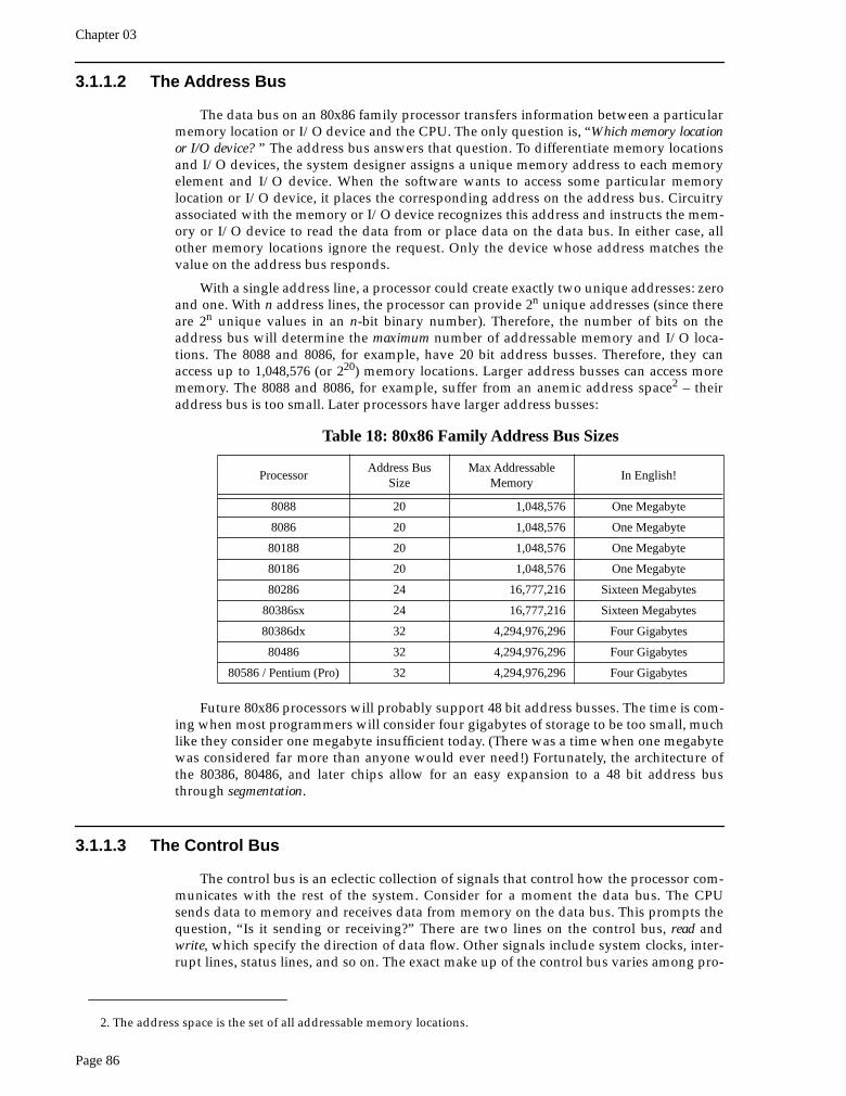
3.1.1.2 The Address Bus
The data bus on an 80x86 family processor transfers information between a particularmemory location or I/O device and the CPU. The only question is, “
Which memory locationor I/O device?
” The address bus answers that question. To differentiate memory locationsand I/O devices, the system designer assigns a unique memory address to each memoryelement and I/O device. When the software wants to access some particular memorylocation or I/O device, it places the corresponding address on the address bus. Circuitryassociated with the memory or I/O device recognizes this address and instructs the mem-ory or I/O device to read the data from or place data on the data bus. In either case, allother memory locations ignore the request. Only the device whose address matches thevalue on the address bus responds.
With a single address line, a processor could create exactly two unique addresses: zeroand one. With
n
address lines, the processor can provide 2
n
unique addresses (since thereare 2
n
unique values in an
n
-bit binary number). Therefore, the number of bits on theaddress bus will determine the
maximum
number of addressable memory and I/O loca-tions. The 8088 and 8086, for example, have 20 bit address busses. Therefore, they canaccess up to 1,048,576 (or 2
20
) memory locations. Larger address busses can access morememory. The 8088 and 8086, for example, suffer from an anemic address space
2
– theiraddress bus is too small. Later processors have larger address busses:
Future 80x86 processors will probably support 48 bit address busses. The time is com-ing when most programmers will consider four gigabytes of storage to be too small, muchlike they consider one megabyte insufficient today. (There was a time when one megabytewas considered far more than anyone would ever need!) Fortunately, the architecture ofthe 80386, 80486, and later chips allow for an easy expansion to a 48 bit address busthrough
segmentation
.
3.1.1.3 The Control Bus
The control bus is an eclectic collection of signals that control how the processor com-municates with the rest of the system. Consider for a moment the data bus. The CPUsends data to memory and receives data from memory on the data bus. This prompts thequestion, “Is it sending or receiving?” There are two lines on the control bus,
read
and
write
, which specify the direction of data flow. Other signals include system clocks, inter-rupt lines, status lines, and so on. The exact make up of the control bus varies among pro-
2. The address space is the set of all addressable memory locations.
Table 18: 80x86 Family Address Bus Sizes
ProcessorAddress Bus
SizeMax Addressable
MemoryIn English!
8088 20 1,048,576 One Megabyte
8086 20 1,048,576 One Megabyte
80188 20 1,048,576 One Megabyte
80186 20 1,048,576 One Megabyte
80286 24 16,777,216 Sixteen Megabytes
80386sx 24 16,777,216 Sixteen Megabytes
80386dx 32 4,294,976,296 Four Gigabytes
80486 32 4,294,976,296 Four Gigabytes
80586 / Pentium (Pro) 32 4,294,976,296 Four Gigabytes
System Organization
Page 87
cessors in the 80x86 family. However, some control lines are common to all processors andare worth a brief mention.
The
read
and
write
control lines control the direction of data on the data bus. Whenboth contain a logic one, the CPU and memory-I/O are not communicating with oneanother. If the read line is low (logic zero), the CPU is reading data from memory (that is,the system is transferring data from memory to the CPU). If the write line is low, the sys-tem transfers data from the CPU to memory.
The
byte enable lines
are another set of important control lines
.
These control linesallow 16, 32, and 64 bit processors to deal with smaller chunks of data. Additional detailsappear in the next section.
The 80x86 family, unlike many other processors, provides two distinct address spaces:one for memory and one for I/O. While the memory address busses on various 80x86 pro-cessors vary in size, the I/O address bus on all 80x86 CPUs is 16 bits wide. This allows theprocessor to address up to 65,536 different I/O
locations.
As it turns out, most devices (likethe keyboard, printer, disk drives, etc.) require more than one I/O location. Nonetheless,65,536 I/O locations are more than sufficient for most applications. The original IBM PCdesign only allowed the use of 1,024 of these.
Although the 80x86 family supports two address spaces, it does not have two addressbusses (for I/O and memory). Instead, the system shares the address bus for both I/O andmemory addresses. Additional control lines decide whether the address is intended formemory or I/O. When such signals are active, the I/O devices use the address on the L.O.16 bits of the address bus. When inactive, the I/O devices ignore the signals on theaddress bus (the memory subsystem takes over at that point).
3.1.2 The Memory Subsystem
A typical 80x86 processor addresses a maximum of 2
n
different memory locations,where
n
is the number of bits on the address bus
3
. As you’ve seen already, 80x86 proces-sors have 20, 24, and 32 bit address busses (with 48 bits on the way).
Of course, the first question you should ask is, “What exactly is a memory location?”The 80x86 supports
byte addressable memory
. Therefore, the basic memory unit is a byte. Sowith 20, 24, and 32 address lines, the 80x86 processors can address one megabyte, 16megabytes, and four gigabytes of memory, respectively.
Think of memory as a linear array of bytes. The address of the first byte is zero and theaddress of the last byte is 2
n
-1. For an 8088 with a 20 bit address bus, the followingpseudo-Pascal array declaration is a good approximation of memory:
Memory: array [0..1048575] of byte;
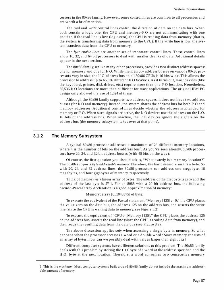
To execute the equivalent of the Pascal statement “Memory [125] := 0;” the CPU placesthe value zero on the data bus, the address 125 on the address bus, and asserts the writeline (since the CPU is writing data to memory, see Figure 3.2)
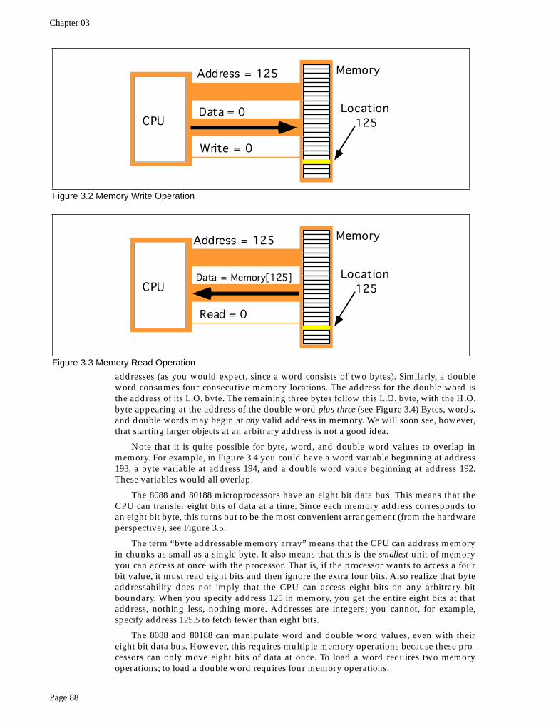
To execute the equivalent of “CPU := Memory [125];” the CPU places the address 125on the address bus, asserts the read line (since the CPU is reading data from memory), andthen reads the resulting data from the data bus (see Figure 3.2).
The above discussion applies
only
when accessing a single byte in memory. So whathappens when the processor accesses a word or a double word? Since memory consists ofan array of bytes, how can we possibly deal with values larger than eight bits?
Different computer systems have different solutions to this problem. The 80x86 familydeals with this problem by storing the L.O. byte of a word at the address specified and theH.O. byte at the next location. Therefore, a word consumes two consecutive memory
3. This is the
maximum
. Most computer systems built around 80x86 family do not include the maximum address-able amount of memory.
Chapter 03
Page 88
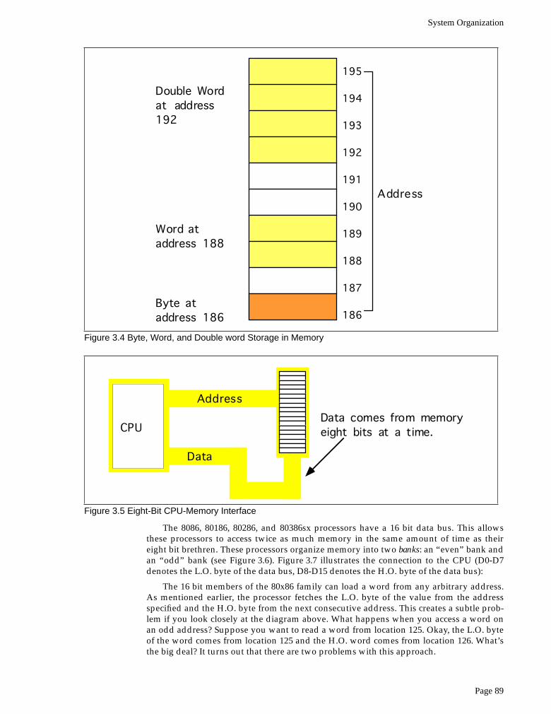
addresses (as you would expect, since a word consists of two bytes). Similarly, a doubleword consumes four consecutive memory locations. The address for the double word isthe address of its L.O. byte. The remaining three bytes follow this L.O. byte, with the H.O.byte appearing at the address of the double word
plus three
(see Figure 3.4) Bytes, words,and double words may begin at
any
valid address in memory. We will soon see, however,that starting larger objects at an arbitrary address is not a good idea.
Note that it is quite possible for byte, word, and double word values to overlap inmemory. For example, in Figure 3.4 you could have a word variable beginning at address193, a byte variable at address 194, and a double word value beginning at address 192.These variables would all overlap.
The 8088 and 80188 microprocessors have an eight bit data bus. This means that theCPU can transfer eight bits of data at a time. Since each memory address corresponds toan eight bit byte, this turns out to be the most convenient arrangement (from the hardwareperspective), see Figure 3.5.
The term “byte addressable memory array” means that the CPU can address memoryin chunks as small as a single byte. It also means that this is the
smallest
unit of memoryyou can access at once with the processor. That is, if the processor wants to access a fourbit value, it must read eight bits and then ignore the extra four bits. Also realize that byteaddressability does not imply that the CPU can access eight bits on any arbitrary bitboundary. When you specify address 125 in memory, you get the entire eight bits at thataddress, nothing less, nothing more. Addresses are integers; you cannot, for example,specify address 125.5 to fetch fewer than eight bits.
The 8088 and 80188 can manipulate word and double word values, even with theireight bit data bus. However, this requires multiple memory operations because these pro-cessors can only move eight bits of data at once. To load a word requires two memoryoperations; to load a double word requires four memory operations.
Figure 3.2 Memory Write Operation
CPU
MemoryAddress = 125
Data = 0
Write = 0
Location 125
Figure 3.3 Memory Read Operation
CPU
MemoryAddress = 125
Data = Memory[125]
Read = 0
Location 125
System Organization
Page 89
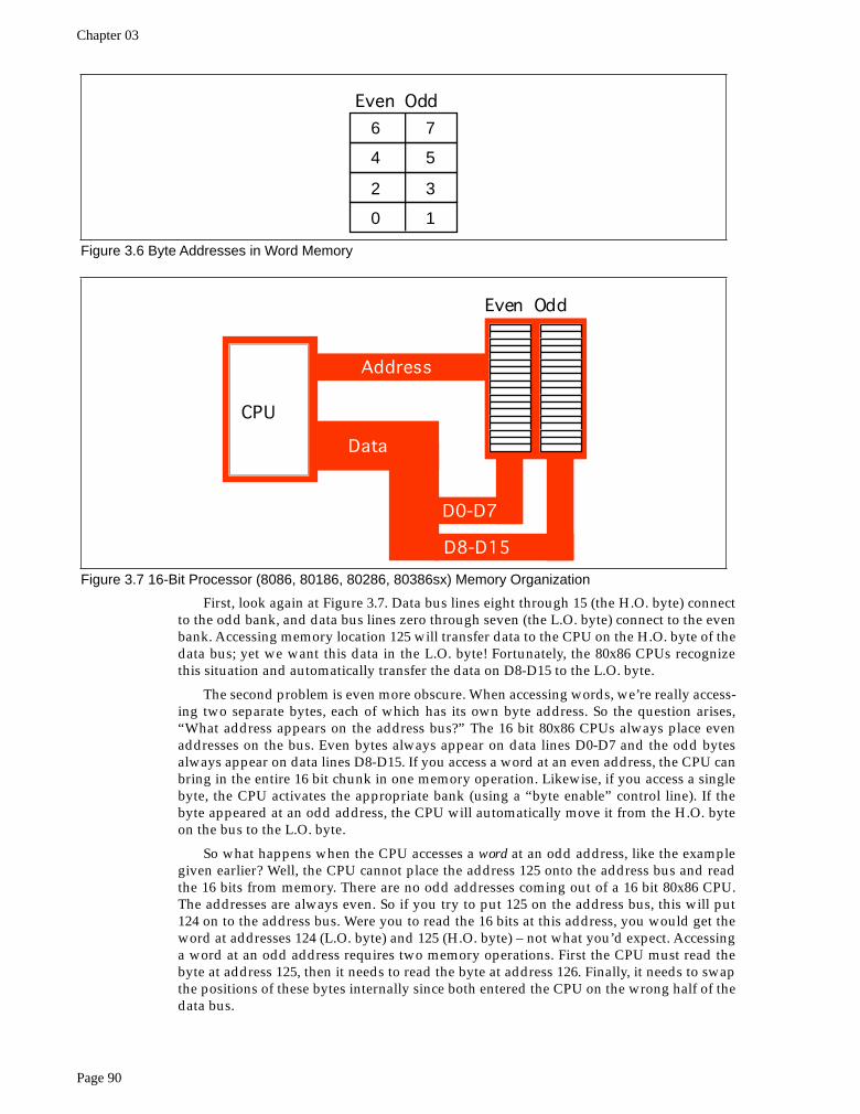
The 8086, 80186, 80286, and 80386sx processors have a 16 bit data bus. This allowsthese processors to access twice as much memory in the same amount of time as theireight bit brethren. These processors organize memory into two
banks
: an “even” bank andan “odd” bank (see Figure 3.6). Figure 3.7 illustrates the connection to the CPU (D0-D7denotes the L.O. byte of the data bus, D8-D15 denotes the H.O. byte of the data bus):
The 16 bit members of the 80x86 family can load a word from any arbitrary address.As mentioned earlier, the processor fetches the L.O. byte of the value from the addressspecified and the H.O. byte from the next consecutive address. This creates a subtle prob-lem if you look closely at the diagram above. What happens when you access a word onan odd address? Suppose you want to read a word from location 125. Okay, the L.O. byteof the word comes from location 125 and the H.O. word comes from location 126. What’sthe big deal? It turns out that there are two problems with this approach.
Figure 3.4 Byte, Word, and Double word Storage in Memory
195
194
193
192
191
190
189
188
187
186
Double Wordat address192
Word ataddress 188
Byte ataddress 186
Address
Figure 3.5 Eight-Bit CPU-Memory Interface
CPU
Address
Data
Data comes from memoryeight bits at a time.
Chapter 03
Page 90
First, look again at Figure 3.7. Data bus lines eight through 15 (the H.O. byte) connectto the odd bank, and data bus lines zero through seven (the L.O. byte) connect to the evenbank. Accessing memory location 125 will transfer data to the CPU on the H.O. byte of thedata bus; yet we want this data in the L.O. byte! Fortunately, the 80x86 CPUs recognizethis situation and automatically transfer the data on D8-D15 to the L.O. byte.
The second problem is even more obscure. When accessing words, we’re really access-ing two separate bytes, each of which has its own byte address. So the question arises,“What address appears on the address bus?” The 16 bit 80x86 CPUs always place evenaddresses on the bus. Even bytes always appear on data lines D0-D7 and the odd bytesalways appear on data lines D8-D15. If you access a word at an even address, the CPU canbring in the entire 16 bit chunk in one memory operation. Likewise, if you access a singlebyte, the CPU activates the appropriate bank (using a “byte enable” control line). If thebyte appeared at an odd address, the CPU will automatically move it from the H.O. byteon the bus to the L.O. byte.
So what happens when the CPU accesses a
word
at an odd address, like the examplegiven earlier? Well, the CPU cannot place the address 125 onto the address bus and readthe 16 bits from memory. There are no odd addresses coming out of a 16 bit 80x86 CPU.The addresses are always even. So if you try to put 125 on the address bus, this will put124 on to the address bus. Were you to read the 16 bits at this address, you would get theword at addresses 124 (L.O. byte) and 125 (H.O. byte) – not what you’d expect. Accessinga word at an odd address requires two memory operations. First the CPU must read thebyte at address 125, then it needs to read the byte at address 126. Finally, it needs to swapthe positions of these bytes internally since both entered the CPU on the wrong half of thedata bus.
Figure 3.6 Byte Addresses in Word Memory
Even Odd
0 1
2 3
4 5
6 7
Figure 3.7 16-Bit Processor (8086, 80186, 80286, 80386sx) Memory Organization
CPU
Address
Data
D0-D7
D8-D15
Even Odd
System Organization
Page 91
Fortunately, the 16 bit 80x86 CPUs hide these details from you. Your programs canaccess words at
any
address and the CPU will properly access and swap (if necessary) thedata in memory. However, to access a word at an odd address requires two memory oper-ations (just like the 8088/80188). Therefore, accessing words at odd addresses on a 16 bitprocessor is slower than accessing words at even addresses.
By carefully arranging howyou use memory, you can improve the speed of your program.
Accessing 32 bit quantities always takes at least two memory operations on the 16 bitprocessors. If you access a 32 bit quantity at an odd address, the processor will requirethree memory operations to access the data.
The 32 bit 80x86 processors (the 80386, 80486, and Pentium Overdrive) use four banksof memory connected to the 32 bit data bus (see Figure 3.8). The address placed on theaddress bus is always some multiple of four. Using various “byte enable” lines, the CPUcan select which of the four bytes at that address the software wants to access. As with the16 bit processor, the CPU will automatically rearrange bytes as necessary.
With a 32 bit memory interface, the 80x86 CPU can access any byte with one memoryoperation. If (address MOD 4) does not equal three, then a 32 bit CPU can access a word atthat address using a single memory operation. However, if the remainder is three, then itwill take two memory operations to access that word (see Figure 3.9). This is the sameproblem encountered with the 16 bit processor, except it occurs half as often.
A 32 bit CPU can access a double word in a single memory operation
if
the address ofthat value is evenly divisible by four. If not, the CPU will require two memory operations.
Once again, the CPU handles all of this automatically. In terms of loading correct datathe CPU handles everything for you. However, there is a performance benefit to properdata alignment. As a general rule you should always place word values at even addressesand double word values at addresses which are evenly divisible by four. This will speedup your program.
Figure 3.8 32-Bit Processor (80386, 80486, Pentium Overdrive) Memory Organization
CPU
Address
Data
D0-D7
D8-D15
D16-D23
D24-D31
Byte 0 1 2 3
Figure 3.9 Accessing a Word at (Address mod 4) = 3.

Chapter 03
Page 92
3.1.3 The I/O Subsystem
Besides the 20, 24, or 32 address lines which access memory, the 80x86 family providesa 16 bit I/O address bus. This gives the 80x86 CPUs two separate address spaces: one formemory and one for I/O operations. Lines on the control bus differentiate between mem-ory and I/O addresses. Other than separate control lines and a smaller bus, I/O address-ing behaves exactly like memory addressing. Memory and I/O devices both share thesame data bus and the L.O. 16 lines on the address bus.
There are three limitations to the I/O subsystem on the IBM PC: first, the 80x86 CPUsrequire special instructions to access I/O devices; second, the designers of the IBM PCused the “best” I/O locations for their own purposes, forcing third party developers touse less accessible locations; third, 80x86 systems can address no more than 65,536 (2
16
)I/O addresses. When you consider that a typical VGA display card requires over 128,000different locations, you can see a problem with the size of I/O bus.
Fortunately, hardware designers can map their I/O devices into the memory addressspace as easily as they can the I/O address space. So by using the appropriate circuitry,they can make their I/O devices look just like memory. This is how, for example, displayadapters on the IBM PC work.
Accessing I/O devices is a subject we’ll return to in later chapters. For right now youcan assume that I/O and memory accesses work the same way.
3.2 System Timing
Although modern computers are quite fast and getting faster all the time, they stillrequire a finite amount of time to accomplish even the smallest tasks. On Von Neumannmachines, like the 80x86, most operations are
serialized
. This means that the computer exe-cutes commands in a prescribed order. It wouldn’t do, for example, to execute the state-ment
I:=I*5+2
; before I
:=J
; in the following sequence:
I := J;I := I * 5 + 2;
Clearly we need some way to control which statement executes first and which executessecond.
Of course, on real computer systems, operations do not occur instantaneously. Mov-ing a copy of
J
into
I
takes a certain amount of time. Likewise, multiplying
I
by five andthen adding two and storing the result back into
I
takes time. As you might expect, the sec-ond Pascal statement above takes quite a bit longer to execute than the first. For thoseinterested in writing fast software, a natural question to ask is, “How does the processorexecute statements, and how do we measure how long they take to execute?”
The CPU is a very complex piece of circuitry. Without going into too many details, letus just say that operations inside the CPU must be very carefully coordinated or the CPUwill produce erroneous results. To ensure that all operations occur at just the rightmoment, the 80x86 CPUs use an alternating signal called the
system clock
.
3.2.1 The System Clock
At the most basic level, the
system clock
handles all synchronization within a computersystem. The system clock is an electrical signal on the control bus which alternatesbetween zero and one at a periodic rate (see Figure 3.10). CPUs are a good example of acomplex synchronous logic system (see the previous chapter). The system clock gatesmany of the logic gates that make up the CPU allowing them to operate in a synchronizedfashion.
System Organization
Page 93
The frequency with which the system clock alternates between zero and one is the
sys-tem clock frequency
. The time it takes for the system clock to switch from zero to one andback to zero is the
clock period.
One full period is also called a
clock cycle
. On most modernsystems, the system clock switches between zero and one at rates exceeding several mil-lion times per second. The clock frequency is simply the number of clock cycles whichoccur each second. A typical 80486 chip runs at speeds of 66million cycles per second.“Hertz” (Hz) is the technical term meaning one cycle per second. Therefore, the aforemen-tioned 80486 chip runs at 66 million hertz, or 66 megahertz (MHz). Typical frequencies for80x86 parts range from 5 MHz up to 200 MHz and beyond. Note that one clock period (theamount of time for one complete clock cycle) is the reciprocal of the clock frequency. Forexample, a 1 MHz clock would have a clock period of one microsecond (1/1,000,000
th
of asecond). Likewise, a 10 MHz clock would have a clock period of 100 nanoseconds (100 bil-lionths of a second). A CPU running at 50 MHz would have a clock period of 20 nanosec-onds. Note that we usually express clock periods in millionths or billionths of a second.
To ensure synchronization, most CPUs start an operation on either the
falling edge
(when the clock goes from one to zero) or the
rising edge
(when the clock goes from zero toone). The system clock spends most of its time at either zero or one and very little timeswitching between the two. Therefore clock edge is the perfect synchronization point.
Since all CPU operations are synchronized around the clock, the CPU cannot performtasks any faster than the clock
4
. However, just because a CPU is running at some clock fre-quency doesn’t mean that it is executing that many operations each second. Many opera-tions take multiple clock cycles to complete so the CPU often performs operations at asignificantly lower rate.
3.2.2 Memory Access and the System Clock
Memory access is probably the most common CPU activity. Memory access is defi-nitely an operation synchronized around the system clock. That is, reading a value frommemory or writing a value to memory occurs no more often than once every clock cycle
5
.Indeed, on many 80x86 processors, it takes several clock cycles to access a memory loca-tion. The
memory access time
is the number of clock cycles the system requires to access amemory location; this is an important value since longer memory access times result inlower performance.
Different 80x86 processors have different memory access times ranging from one tofour clock cycles. For example, the 8088 and 8086 CPUs require
four
clock cycles to accessmemory; the 80486 requires only one. Therefore, the 80486 will execute programs whichaccess memory faster than an 8086, even when running at the same clock frequency.
4. Some later versions of the 80486 use special clock doubling circuitry to run twice as fast as the input clock fre-quency. For example, with a 25 MHz clock the chip runs at an effective rate of 50 MHz. However, the internalclock frequency
is
50 MHz. The CPU still won’t execute operations faster than 50 million operations per second.5. This is true even on the clock doubled CPUs.
Figure 3.10 The System Clock
10
Time
One Clock “Period”
Chapter 03
Page 94
Memory access time is the amount of time between a memory operation request (reador write) and the time the memory operation completes. On a 5 MHz 8088/8086 CPU thememory access time is roughly 800 ns (nanoseconds). On a 50 MHz 80486, the memoryaccess time is slightly less than 20 ns. Note that the memory access time for the 80486 is 40times faster than the 8088/8086. This is because the 80486’s clock frequency is ten timesfaster and it uses one-fourth the clock cycles to access memory.
When reading from memory, the memory access time is the amount of time from thepoint that the CPU places an address on the address bus and the CPU takes the data offthe data bus. On an 80486 CPU with a one cycle memory access time, a read looks some-thing like shown in Figure 3.11. Writing data to memory is similar (see Figure 3.11).
Note that the CPU doesn’t wait for memory. The access time is specified by the clockfrequency. If the memory subsystem doesn’t work fast enough, the CPU will read garbagedata on a memory read operation and will not properly store the data on a memory writeoperation. This will surely cause the system to fail.
Memory devices have various ratings, but the two major ones are capacity and speed(access time). Typical dynamic RAM (random access memory) devices have capacities offour (or more) megabytes and speeds of 50-100 ns. You can buy bigger or faster devices,but they are much more expensive. A typical 33 MHz 80486 system uses 70 ns memorydevices.
Wait just a second here! At 33 MHz the clock period is roughly 33 ns. How can a sys-tem designer get away with using 70 ns memory? The answer is
wait states
.
Figure 3.11 An 80486 Memory Read Cycle
The CPU placesthe address onthe address busduring this timeperiod The memory system must
decode the address andplace the data on the databus during this time period
The CPU reads thedata from the databus during this timeperiod
Figure 3.12 An 80486 Memory Write Cycle
The CPU placesthe address anddata onto the busat this time
Sometime before the endof the clock period thememory subsystem mustgrab and store the specifiedvalue
System Organization
Page 95
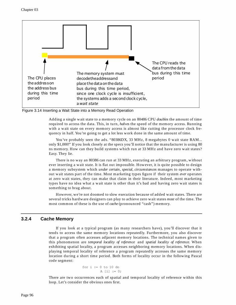
3.2.3 Wait States
A wait state is nothing more than an extra clock cycle to give some device time tocomplete an operation. For example, a 50 MHz 80486 system has a 20 ns clock period. Thisimplies that you need 20 ns memory. In fact, the situation is worse than this. In most com-puter systems there is additional circuitry between the CPU and memory: decoding andbuffering logic. This additional circuitry introduces additional delays into the system (seeFigure 3.13). In this diagram, the system loses 10ns to buffering and decoding. So if theCPU needs the data back in 20 ns, the memory must respond in less than 10 ns.
You can actually buy 10ns memory. However, it is very expensive, bulky, consumes alot of power, and generates a lot of heat. These are bad attributes. Supercomputers use thistype of memory. However, supercomputers also cost millions of dollars, take up entirerooms, require special cooling, and have giant power supplies. Not the kind of stuff youwant sitting on your desk.
If cost-effective memory won’t work with a fast processor, how do companies manageto sell fast PCs? One part of the answer is the wait state. For example, if you have a 20MHz processor with a memory cycle time of 50 ns and you lose 10 ns to buffering anddecoding, you’ll need 40 ns memory. What if you can only afford 80 ns memory in a 20MHz system? Adding a wait state to extend the memory cycle to 100 ns (two clock cycles)will solve this problem. Subtracting 10ns for the decoding and buffering leaves 90 ns.Therefore, 80 ns memory will respond well before the CPU requires the data.
Almost every general purpose CPU in existence provides a signal on the control busto allow the insertion of wait states. Generally, the decoding circuitry asserts this line todelay one additional clock period, if necessary. This gives the memory sufficient accesstime, and the system works properly (see Figure 3.14).
Sometimes a single wait state is not sufficient. Consider the 80486 running at 50 MHz.The normal memory cycle time is less than 20 ns. Therefore, less than 10 ns are availableafter subtracting decoding and buffering time. If you are using 60 ns memory in the sys-tem, adding a single wait state will not do the trick. Each wait state gives you 20 ns, sowith a single wait state you would need 30 ns memory. To work with 60 ns memory youwould need to add three wait states (zero wait states = 10 ns, one wait state = 30 ns, twowait states = 50 ns, and three wait states = 70 ns).
Needless to say, from the system performance point of view, wait states are not a goodthing. While the CPU is waiting for data from memory it cannot operate on that data.
Figure 3.13 Decoding and Buffing Delays
CPU
Decoder
Buffer
address
data
5 ns delaythroughdecoder
5 ns delaythroughbuffer
Chapter 03
Page 96
Adding a single wait state to a memory cycle on an 80486 CPU doubles the amount of timerequired to access the data. This, in turn, halves the speed of the memory access. Runningwith a wait state on every memory access is almost like cutting the processor clock fre-quency in half. You’re going to get a lot less work done in the same amount of time.
You’ve probably seen the ads. “80386DX, 33 MHz, 8 megabytes 0 wait state RAM...only $1,000!” If you look closely at the specs you’ll notice that the manufacturer is using 80ns memory. How can they build systems which run at 33 MHz and have zero wait states?Easy. They lie.
There is no way an 80386 can run at 33 MHz, executing an arbitrary program, withoutever inserting a wait state. It is flat out impossible. However, it is quite possible to designa memory subsystem which under certain, special, circumstances manages to operate with-out wait states part of the time. Most marketing types figure if their system ever operatesat zero wait states, they can make that claim in their literature. Indeed, most marketingtypes have no idea what a wait state is other than it’s bad and having zero wait states issomething to brag about.
However, we’re not doomed to slow execution because of added wait states. There areseveral tricks hardware designers can play to achieve zero wait states most of the time. Themost common of these is the use of cache (pronounced “cash”) memory.
3.2.4 Cache Memory
If you look at a typical program (as many researchers have), you’ll discover that ittends to access the same memory locations repeatedly. Furthermore, you also discoverthat a program often accesses adjacent memory locations. The technical names given tothis phenomenon are temporal locality of reference and spatial locality of reference. Whenexhibiting spatial locality, a program accesses neighboring memory locations. When dis-playing temporal locality of reference a program repeatedly accesses the same memorylocation during a short time period. Both forms of locality occur in the following Pascalcode segment:
for i := 0 to 10 doA [i] := 0;
There are two occurrences each of spatial and temporal locality of reference within thisloop. Let’s consider the obvious ones first.
Figure 3.14 Inserting a Wait State into a Memory Read Operation
The CPU placesthe address onthe address busduring this timeperiod
The memory system mustdecode the address andplace the data on the databus during this time period,since one clock cycle is insufficient,the systems adds a second clock cycle,a wait state
The CPU reads thedata from the databus during this timeperiod
System Organization
Page 97
In the Pascal code above, the program references the variable i several times. The forloop compares i against 10 to see if the loop is complete. It also increments i by one at thebottom of the loop. The assignment statement also uses i as an array index. This showstemporal locality of reference in action since the CPU accesses i at three points in a shorttime period.
This program also exhibits spatial locality of reference. The loop itself zeros out theelements of array A by writing a zero to the first location in A, then to the second locationin A, and so on. Assuming that Pascal stores the elements of A into consecutive memorylocations6, each loop iteration accesses adjacent memory locations.
There is an additional example of temporal and spatial locality of reference in the Pas-cal example above, although it is not so obvious. Computer instructions which tell the sys-tem to do the specified task also appear in memory. These instructions appearsequentially in memory – the spatial locality part. The computer also executes theseinstructions repeatedly, once for each loop iteration – the temporal locality part.
If you look at the execution profile of a typical program, you’d discover that the pro-gram typically executes less than half the statements. Generally, a typical program mightonly use 10-20% of the memory allotted to it. At any one given time, a one megabyte pro-gram might only access four to eight kilobytes of data and code. So if you paid an outra-geous sum of money for expensive zero wait state RAM, you wouldn’t be using most of itat any one given time! Wouldn’t it be nice if you could buy a small amount of fast RAMand dynamically reassign its address(es) as the program executes?
This is exactly what cache memory does for you. Cache memory sits between the CPUand main memory. It is a small amount of very fast (zero wait state) memory. Unlike nor-mal memory, the bytes appearing within a cache do not have fixed addresses. Instead,cache memory can reassign the address of a data object. This allows the system to keeprecently accessed values in the cache. Addresses which the CPU has never accessed orhasn’t accessed in some time remain in main (slow) memory. Since most memory accessesare to recently accessed variables (or to locations near a recently accessed location), thedata generally appears in cache memory.
Cache memory is not perfect. Although a program may spend considerable time exe-cuting code in one place, eventually it will call a procedure or wander off to some sectionof code outside cache memory. In such an event the CPU has to go to main memory tofetch the data. Since main memory is slow, this will require the insertion of wait states.
A cache hit occurs whenever the CPU accesses memory and finds the data in thecache. In such a case the CPU can usually access data with zero wait states. A cache missoccurs if the CPU accesses memory and the data is not present in cache. Then the CPU hasto read the data from main memory, incurring a performance loss. To take advantage oflocality of reference, the CPU copies data into the cache whenever it accesses an addressnot present in the cache. Since it is likely the system will access that same location shortly,the system will save wait states by having that data in the cache.
As described above, cache memory handles the temporal aspects of memory access,but not the spatial aspects. Caching memory locations when you access them won’t speedup the program if you constantly access consecutive locations (spatial locality of refer-ence). To solve this problem, most caching systems read several consecutive bytes frommemory when a cache miss occurs7. The 80486, for example, reads 16 bytes at a shot upona cache miss. If you read 16 bytes, why read them in blocks rather than as you need them?As it turns out, most memory chips available today have special modes which let youquickly access several consecutive memory locations on the chip. The cache exploits thiscapability to reduce the average number of wait states needed to access memory.
If you write a program that randomly accesses memory, using a cache might actuallyslow you down. Reading 16 bytes on each cache miss is expensive if you only access a few
6. It does, see “Memory Layout and Access” on page 145.7. Engineers call this block of data a cache line.
Chapter 03
Page 98
bytes in the corresponding cache line. Nonetheless, cache memory systems work quitewell.
It should come as no surprise that the ratio of cache hits to misses increases with thesize (in bytes) of the cache memory subsystem. The 80486 chip, for example, has 8,192bytes of on-chip cache. Intel claims to get an 80-95% hit rate with this cache (meaning80-95% of the time the CPU finds the data in the cache). This sounds very impressive.However, if you play around with the numbers a little bit, you’ll discover it’s not all thatimpressive. Suppose we pick the 80% figure. Then one out of every five memory accesses,on the average, will not be in the cache. If you have a 50 MHz processor and a 90 ns mem-ory access time, four out of five memory accesses require only one clock cycle (since theyare in the cache) and the fifth will require about 10 wait states8. Altogether, the systemwill require 15 clock cycles to access five memory locations, or three clock cycles peraccess, on the average. That’s equivalent to two wait states added to every memoryaccess. Now do you believe that your machine runs at zero wait states?
There are a couple of ways to improve the situation. First, you can add more cachememory. This improves the cache hit ratio, reducing the number of wait states. For exam-ple, increasing the hit ratio from 80% to 90% lets you access 10 memory locations in 20cycles. This reduces the average number of wait states per memory access to one waitstate – a substantial improvement. Alas, you can’t pull an 80486 chip apart and soldermore cache onto the chip. However, the 80586/Pentium CPU has a significantly largercache than the 80486 and operates with fewer wait states.
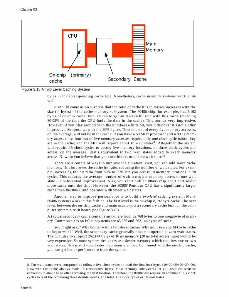
Another way to improve performance is to build a two-level caching system. Many80486 systems work in this fashion. The first level is the on-chip 8,192 byte cache. The nextlevel, between the on-chip cache and main memory, is a secondary cache built on the com-puter system circuit board (see Figure 3.15).
A typical secondary cache contains anywhere from 32,768 bytes to one megabyte of mem-ory. Common sizes on PC subsystems are 65,536 and 262,144 bytes of cache.
You might ask, “Why bother with a two-level cache? Why not use a 262,144 byte cacheto begin with?” Well, the secondary cache generally does not operate at zero wait states.The circuitry to support 262,144 bytes of 10 ns memory (20 ns total access time) would bevery expensive. So most system designers use slower memory which requires one or twowait states. This is still much faster than main memory. Combined with the on-chip cache,you can get better performance from the system.
8. Ten wait states were computed as follows: five clock cycles to read the first four bytes (10+20+20+20+20=90).However, the cache always reads 16 consecutive bytes. Most memory subsystems let you read consecutiveaddresses in about 40 ns after accessing the first location. Therefore, the 80486 will require an additional six clockcycles to read the remaining three double words. The total is 11 clock cycles or 10 wait states.
Figure 3.15 A Two Level Caching System
CPU
On-chip (primary)cache Secondary Cache
MainMemory
System Organization
Page 99
Consider the previous example with an 80% hit ratio. If the secondary cache requirestwo cycles for each memory access and three cycles for the first access, then a cache misson the on-chip cache will require a total of six clock cycles. All told, the average systemperformance will be two clocks per memory access. Quite a bit faster than the threerequired by the system without the secondary cache. Furthermore, the secondary cachecan update its values in parallel with the CPU. So the number of cache misses (whichaffect CPU performance) goes way down.
You’re probably thinking, “So far this all sounds interesting, but what does it have todo with programming?” Quite a bit, actually. By writing your program carefully to takeadvantage of the way the cache memory system works, you can improve your program’sperformance. By colocating variables you commonly use together in the same cache line,you can force the cache system to load these variables as a group, saving extra wait stateson each access.
If you organize your program so that it tends to execute the same sequence of instruc-tions repeatedly, it will have a high degree of temporal locality of reference and will, there-fore, execute faster.
3.3 The 886, 8286, 8486, and 8686 “Hypothetical” Processors
To understand how to improve system performance, it’s time to explore the internaloperation of the CPU. Unfortunately, the processors in the 80x86 family are complexbeasts. Discussing their internal operation would probably cause more confusion thanenlightenment. So we will use the 886, 8286, 8486, and 8686 processors (the “x86” proces-sors). These “paper processors” are extreme simplifications of various members of the80x86 family. They highlight the important architectural features of the 80x86.
The 886, 8286, 8486, and 8686 processors are all identical except for the way they exe-cute instructions. They all have the same register set, and they “execute” the same instruc-tion set. That sentence contains some new ideas; let’s attack them one at a time.
3.3.1 CPU Registers
CPU registers are very special memory locations constructed from flip-flops. They arenot part of main memory; the CPU implements them on-chip. Various members of the80x86 family have different register sizes. The 886, 8286, 8486, and 8686 (x86 from now on)CPUs have exactly four registers, all 16 bits wide. All arithmetic and location operationsoccur in the CPU registers.
Because the x86 processor has so few registers, we’ll give each register its own nameand refer to it by that name rather than its address. The names for the x86 registers are
AX –The accumulator registerBX –The base address registerCX –The count registerDX –The data register
Besides the above registers, which are visible to the programmer, the x86 processors alsohave an instruction pointer register which contains the address of the next instruction toexecute. There is also a flags register that holds the result of a comparison. The flags regis-ter remembers if one value was less than, equal to, or greater than another value.
Because registers are on-chip and handled specially by the CPU, they are much fasterthan memory. Accessing a memory location requires one or more clock cycles. Accessingdata in a register usually takes zero clock cycles. Therefore, you should try to keep vari-ables in the registers. Register sets are very small and most registers have special purposeswhich limit their use as variables, but they are still an excellent place to store temporarydata.
Chapter 03
Page 100
3.3.2 The Arithmetic & Logical Unit
The arithmetic and logical unit (ALU) is where most of the action takes place insidethe CPU. For example, if you want to add the value five to the AX register, the CPU:
• Copies the value from AX into the ALU, • Sends the value five to the ALU, • Instructs the ALU to add these two values together, • Moves the result back into the AX register.
3.3.3 The Bus Interface Unit
The bus interface unit (BIU) is responsible for controlling the address and data busseswhen accessing main memory. If a cache is present on the CPU chip then the BIU is alsoresponsible for accessing data in the cache.
3.3.4 The Control Unit and Instruction Sets
A fair question to ask at this point is “How exactly does a CPU perform assignedchores?” This is accomplished by giving the CPU a fixed set of commands, or instructions,to work on. Keep in mind that CPU designers construct these processors using logic gatesto execute these instructions. To keep the number of logic gates to a reasonably small set(tens or hundreds of thousands), CPU designers must necessarily restrict the number andcomplexity of the commands the CPU recognizes. This small set of commands is theCPU’s instruction set.
Programs in early (pre-Von Neumann) computer systems were often “hard-wired”into the circuitry. That is, the computer’s wiring determined what problem the computerwould solve. One had to rewire the circuitry in order to change the program. A very diffi-cult task. The next advance in computer design was the programmable computer system,one that allowed a computer programmer to easily “rewire” the computer system using asequence of sockets and plug wires. A computer program consisted of a set of rows ofholes (sockets), each row representing one operation during the execution of the program.The programmer could select one of several instructions by plugging a wire into the par-ticular socket for the desired instruction (see Figure 3.16). Of course, a major difficultywith this scheme is that the number of possible instructions is severely limited by thenumber of sockets one could physically place on each row. However, CPU designersquickly discovered that with a small amount of additional logic circuitry, they couldreduce the number of sockets required from n holes for n instructions to log2(n) holes for ninstructions. They did this by assigning a numeric code to each instruction and then
Figure 3.16 Patch Panel Programming
Instr #1
Instr #2
Instr #3 . . .
mov
e
add
subt
ract
mul
tiply
divi
de
and
or xor
System Organization
Page 101
encode that instruction as a binary number using log2(n) holes (see Figure 3.17). Thisaddition requires eight logic functions to decode the A, B, and C bits from the patch panel,but the extra circuitry is well worth the cost because it reduces the number of sockets thatmust be repeated for each instruction.
Of course, many CPU instructions are not stand-alone. For example, the move instruc-tion is a command that moves data from one location in the computer to another (e.g.,from one register to another). Therefore, the move instruction requires two operands: asource operand and a destination operand. The CPU’s designer usually encodes these sourceand destination operands as part of the machine instruction, certain sockets correspond tothe source operand and certain sockets correspond to the destination operand.Figure 3.17 shows one possible combination of sockets to handle this. The move instruc-tion would move data from the source register to the destination register, the add instruc-tion would add the value of the source register to the destination register, etc.
One of the primary advances in computer design that the VNA provides is the con-cept of a stored program. One big problem with the patch panel programming method isthat the number of program steps (machine instructions) is limited by the number of rowsof sockets available on the machine. John Von Neumann and others recognized a relation-ship between the sockets on the patch panel and bits in memory; they figured they couldstore the binary equivalents of a machine program in main memory and fetch each pro-gram from memory, load it into a special decoding register that connected directly to theinstruction decoding circuitry of the CPU.
Figure 3.17 Encoding Instructions
Instr #1
Instr #2
Instr #3 . . .
C B A CBA Instruction000 move001 add010 subtract011 multiply100 divide101 and110 or111 xor
Figure 3.18 Encoding Instructions with Source and Destination Fields
Instr #1
Instr #2
Instr #3 . . .
C B A
CBA Instruction000 move001 add010 subtract011 multiply100 divide101 and110 or111 xor
DD SS
DD -or- SS Register
00 AX 01 BX 10 CX 11 DX
Chapter 03
Page 102
The trick, of course, was to add yet more circuitry to the CPU. This circuitry, the con-trol unit (CU), fetches instruction codes (also known as operation codes or opcodes) frommemory and moves them to the instruction decoding register. The control unit contains aspecial registers, the instruction pointer that contains the address of an executable instruc-tion. The control unit fetches this instruction’s code from memory and places it in thedecoding register for execution. After executing the instruction, the control unit incre-ments the instruction pointer and fetches the next instruction from memory for execution,and so on.
When designing an instruction set, the CPU’s designers generally choose opcodes thatare a multiple of eight bits long so the CPU can easily fetch complete instructions frommemory. The goal of the CPU’s designer is to assign an appropriate number of bits to theinstruction class field (move, add, subtract, etc.) and to the operand fields. Choosing morebits for the instruction field lets you have more instructions, choosing additional bits forthe operand fields lets you select a larger number of operands (e.g., memory locations orregisters). There are additional complications. Some instructions have only one operandor, perhaps, they don’t have any operands at all. Rather than waste the bits associatedwith these fields, the CPU designers often reuse these fields to encode additional opcodes,once again with some additional circuitry. The Intel 80x86 CPU family takes this to anextreme with instructions ranging from one to about ten bytes long. Since this is a little toodifficult to deal with at this early stage, the x86 CPUs will use a different, much simpler,encoding scheme.
3.3.5 The x86 Instruction Set
The x86 CPUs provide 20 basic instruction classes. Seven of these instructions havetwo operands, eight of these instructions have a single operand, and five instructions haveno operands at all. The instructions are mov (two forms), add, sub, cmp, and, or, not, je, jne,jb, jbe, ja, jae, jmp, brk, iret, halt, get, and put. The following paragraphs describe how each ofthese work.
The mov instruction is actually two instruction classes merged into the same instruc-tion. The two forms of the mov instruction take the following forms:
mov reg, reg/memory/constantmov memory, reg
where reg is any of ax, bx, cx, or dx; constant is a numeric constant (using hexadecimal nota-tion), and memory is an operand specifying a memory location. The next section describesthe possible forms the memory operand can take. The “reg/memory/constant” operandtells you that this particular operand may be a register, memory location, or a constant.
The arithmetic and logical instructions take the following forms:
add reg, reg/memory/constantsub reg, reg/memory/constantcmp reg, reg/memory/constantand reg, reg/memory/constantor reg, reg/memory/constantnot reg/memory
The add instruction adds the value of the second operand to the first (register) operand,leaving the sum in the first operand. The sub instruction subtracts the value of the secondoperand from the first, leaving the difference in the first operand. The cmp instructioncompares the first operand against the second and saves the result of this comparison foruse with one of the conditional jump instructions (described in a moment). The and and orinstructions compute the corresponding bitwise logical operation on the two operandsand store the result into the first operand. The not instruction inverts the bits in the singlememory or register operand.
The control transfer instructions interrupt the sequential execution of instructions inmemory and transfer control to some other point in memory either unconditionally, or
System Organization
Page 103
after testing the result of the previous cmp instruction. These instructions include the fol-lowing:
ja dest -- Jump if abovejae dest -- Jump if above or equaljb dest -- Jump if belowjbe dest -- Jump if below or equalje dest -- Jump if equaljne dest -- Jump if not equaljmp dest -- Unconditional jumpiret -- Return from an interrupt
The first six instructions in this class let you check the result of the previous cmp instruc-tion for greater than, greater or equal, less than, less or equal, equality, or inequality9. Forexample, if you compare the ax and bx registers with the cmp instruction and execute the jainstruction, the x86 CPU will jump to the specified destination location if ax was greaterthan bx. If ax is not greater than bx, control will fall through to the next instruction in theprogram. The jmp instruction unconditionally transfers control to the instruction at thedestination address. The iret instruction returns control from an interrupt service routine,which we will discuss later.
The get and put instructions let you read and write integer values. Get will stop andprompt the user for a hexadecimal value and then store that value into the ax register. Putdisplays (in hexadecimal) the value of the ax register.
The remaining instructions do not require any operands, they are halt and brk. Halt ter-minates program execution and brk stops the program in a state that it can be restarted.
The x86 processors require a unique opcode for every different instruction, not just theinstruction classes. Although “mov ax, bx” and “mov ax, cx” are both in the same class,they must have different opcodes if the CPU is to differentiate them. However, beforelooking at all the possible opcodes, perhaps it would be a good idea to learn about all thepossible operands for these instructions.
3.3.6 Addressing Modes on the x86
The x86 instructions use five different operand types: registers, constants, and threememory addressing schemes. Each form is called an addressing mode. The x86 processorssupport the register addressing mode10, the immediate addressing mode, the indirectaddressing mode, the indexed addressing mode, and the direct addressing mode. The fol-lowing paragraphs explain each of these modes.
Register operands are the easiest to understand. Consider the following forms of themov instruction:
mov ax, axmov ax, bxmov ax, cxmov ax, dx
The first instruction accomplishes absolutely nothing. It copies the value from the axregister back into the ax register. The remaining three instructions copy the value of bx, cxand dx into ax. Note that the original values of bx, cx, and dx remain the same. The firstoperand (the destination) is not limited to ax; you can move values to any of these registers.
Constants are also pretty easy to deal with. Consider the following instructions:
mov ax, 25mov bx, 195mov cx, 2056mov dx, 1000
9. The x86 processors only performed unsigned comparisons. 10. Technically, registers do not have an address, but we apply the term addressing mode to registers nonetheless.
Chapter 03
Page 104
These instructions are all pretty straightforward; they load their respective registers withthe specified hexadecimal constant11.
There are three addressing modes which deal with accessing data in memory. Theseaddressing modes take the following forms:
mov ax, [1000]mov ax, [bx]mov ax, [1000+bx]
The first instruction above uses the direct addressing mode to load ax with the 16 bitvalue stored in memory starting at location 1000 hex.
The mov ax, [bx] instruction loads ax from the memory location specified by thecontents of the bx register. This is an indirect addressing mode. Rather than using the valuein bx, this instruction accesses to the memory location whose address appears in bx. Notethat the following two instructions:
mov bx, 1000mov ax, [bx]
are equivalent to the single instruction:
mov ax, [1000]
Of course, the second sequence is preferable. However, there are many cases where theuse of indirection is faster, shorter, and better. We’ll see some examples of this when welook at the individual processors in the x86 family a little later.
The last memory addressing mode is the indexed addressing mode. An example of thismemory addressing mode is
mov ax, [1000+bx]
This instruction adds the contents of bx with 1000 to produce the address of the memoryvalue to fetch. This instruction is useful for accessing elements of arrays, records, andother data structures.
3.3.7 Encoding x86 Instructions
Although we could arbitrarily assign opcodes to each of the x86 instructions, keep inmind that a real CPU uses logic circuitry to decode the opcodes and act appropriately onthem. A typical CPU opcode uses a certain number of bits in the opcode to denote theinstruction class (e.g., mov, add, sub), and a certain number of bits to encode each of theoperands. Some systems (e.g., CISC, or Complex Instruction Set Computers) encode thesefields in a very complex fashion producing very compact instructions. Other systems (e.g.,RISC, or Reduced Instruction Set Computers) encode the opcodes in a very simple fashioneven if it means wasting some bits in the opcode or limiting the number of operations. TheIntel 80x86 family is definitely CISC and has one of the most complex opcode decodingschemes ever devised. The whole purpose for the hypothetical x86 processors is to presentthe concept of instruction encoding without the attendant complexity of the 80x86 family,while still demonstrating CISC encoding.
A typical x86 instruction takes the form shown in Figure 3.19. The basic instruction iseither one or three bytes long. The instruction opcode consists of a single byte that con-tains three fields. The first field, the H.O. three bits, defines the instruction class. This pro-vides eight combinations. As you may recall, there are 20 instruction classes; we cannotencode 20 instruction classes with three bits, so we’ll have to pull some tricks to handlethe other classes. As you can see in Figure 3.19, the basic opcode encodes the mov instruc-tions (two classes, one where the rr field specifies the destination, one where the mmmfield specifies the destination), the add, sub, cmp, and, and or instructions. There is one
11. All numeric constants on the x86 are given in hexadecimal. The “h” suffix is not necessary.

System Organization
Page 105
additional class: special. The special instruction class provides a mechanism that allows usto expand the number of available instruction classes, we will return to this class shortly.
To determine a particular instruction’s opcode, you need only select the appropriatebits for the iii, rr, and mmm fields. For example, to encode the mov ax, bx instruction youwould select iii=110 (mov reg, reg), rr=00 (ax), and mmm=001 (bx). This produces theone-byte instruction 11000001 or 0C0h.
Some x86 instructions require more than one byte. For example, the instructionmov ax, [1000] loads the ax register from memory location 1000. The encoding for theopcode is 11000110 or 0C6h. However, the encoding for mov ax,[2000]’s opcode is also0C6h. Clearly these two instructions do different things, one loads the ax register frommemory location 1000h while the other loads the ax register from memory location 2000.To encode an address for the [xxxx] or [xxxx+bx] addressing modes, or to encode the con-stant for the immediate addressing mode, you must follow the opcode with the 16-bitaddress or constant, with the L.O. byte immediately following the opcode in memory andthe H.O. byte after that. So the three byte encoding for mov ax, [1000] would be 0C6h, 00h,10h12 and the three byte encoding for mov ax, [2000] would be 0C6h, 00h, 20h.
The special opcode allows the x86 CPU to expand the set of available instructions.This opcode handles several zero and one-operand instructions as shown in Figure 3.20and Figure 3.21.
12. Remember, all numeric constants are hexadecimal.
Figure 3.19 Basic x86 Instruction Encoding.
i i i r r m m m
i i i
000 = special001 = or010 = and011 = cmp100 = sub101 = add110 = mov reg, mem/reg/const111 = mov mem, reg
r r
00 = AX01 = BX10 = CX11 = DX
mmm
0 0 0 = AX0 0 1 = BX0 1 0 = CX0 1 1 = DX1 0 0 = [BX]1 0 1 = [xxxx+BX]1 1 0 = [xxxx]1 1 1 = constant
This 16-bit field is presentonly if the instruction is ajump instruction or an operandis a memory addressing modeof the form [bx+xxxx], [xxxxx],or a constant.
Figure 3.20 Single Operand Instruction Encodings
0 0 0 i i m m m
i i
00 = zero operand instructions01 = jump instructions10 = not11 = illegal (reserved)
mmm (if ii = 10)
000 = AX001 = BX010 = CX011 = DX100 = [BX]101 = [ xxxx+BX]110 = [ xxxx]111 = constant
This 16-bit field is presentonly if the instruction is ajump instruction or an operandis a memory addressing modeof the form [bx+xxxx], [xxxxx],or a constant.

Chapter 03
Page 106
There are four one-operand instruction classes. The first encoding (00) furtherexpands the instruction set with a set of zero-operand instructions (see Figure 3.21). Thesecond opcode is also an expansion opcode that provides all the x86 jump instructions (seeFigure 3.22). The third opcode is the not instruction. This is the bitwise logical not opera-tion that inverts all the bits in the destination register or memory operand. The fourth sin-gle-operand opcode is currently unassigned. Any attempt to execute this opcode will haltthe processor with an illegal instruction error. CPU designers often reserve unassignedopcodes like this one to extend the instruction set at a future date (as Intel did when mov-ing from the 80286 processor to the 80386).
There are seven jump instructions in the x86 instruction set. They all take the follow-ing form:
jxx address
The jmp instruction copies the 16-bit immediate value (address) following the opcodeinto the IP register. Therefore, the CPU will fetch the next instruction from this targetaddress; effectively, the program “jumps” from the point of the jmp instruction to theinstruction at the target address.
The jmp instruction is an example of an unconditional jump instruction. It always trans-fers control to the target address. The remaining six instructions are conditional jumpinstructions. They test some condition and jump if the condition is true; they fall throughto the next instruction if the condition is false. These six instructions, ja, jae, jb, jbe, je, andjne let you test for greater than, greater than or equal, less than, less than or equal, equality,and inequality. You would normally execute these instructions immediately after a cmp
Figure 3.21 Zero Operand Instruction Encodings
0 0 0 0 0 i i i
i i i
000 = illegal001 = illegal010 = illegal011 = brk100 = iret101 = halt110 = get111 = put
Figure 3.22 Jump Instruction Encodings
0 0 0 0 1 i i i
mmm (if ii = 10)
000 = j e001 = jne010 = j b011 = jbe100 = j a101 = jae110 = jmp111 = ill egal
This 16-bit field is always presentand contains the target address tojump move into the instructionpointer register if the jumpis taken.
System Organization
Page 107
instruction since it sets the less than and equality flags that the conditional jump instruc-tions test. Note that there are eight possible jump opcodes, but the x86 uses only seven ofthem. The eighth opcode is another illegal opcode.
The last group of instructions, the zero operand instructions, appear in Figure 3.21.Three of these instructions are illegal instruction opcodes. The brk (break) instructionpauses the CPU until the user manually restarts it. This is useful for pausing a programduring execution to observe results. The iret (interrupt return) instruction returns controlfrom an interrupt service routine. We will discuss interrupt service routines later. The haltprogram terminates program execution. The get instruction reads a hexadecimal valuefrom the user and returns this value in the ax register; the put instruction outputs the valuein the ax register.
3.3.8 Step-by-Step Instruction Execution
The x86 CPUs do not complete execution of an instruction in a single clock cycle. TheCPU executes several steps for each instruction. For example, the CU issues the followingcommands to execute the mov reg, reg/memory/constant instruction:
• Fetch the instruction byte from memory.• Update the ip register to point at the next byte.• Decode the instruction to see what it does.• If required, fetch a 16-bit instruction operand from memory.• If required, update ip to point beyond the operand.• Compute the address of the operand, if required (i.e., bx+xxxx) .• Fetch the operand.• Store the fetched value into the destination register
A step-by-step description may help clarify what the CPU is doing. In the first step,the CPU fetches the instruction byte from memory. To do this, it copies the value of the ipregister to the address bus and reads the byte at that address. This will take one clockcycle13.
After fetching the instruction byte, the CPU updates ip so that it points at the next bytein the instruction stream. If the current instruction is a multibyte instruction, ip will nowpoint at the operand for the instruction. If the current instruction is a single byte instruc-tion, ip would be left pointing at the next instruction. This takes one clock cycle.
The next step is to decode the instruction to see what it does. This will tell the CPU,among other things, if it needs to fetch additional operand bytes from memory. This takesone clock cycle.
During decoding, the CPU determines the types of operands the instruction requires.If the instruction requires a 16 bit constant operand (i.e., if the mmm field is 101, 110, or111) then the CPU fetches that constant from memory. This step may require zero, one, ortwo clock cycles. It requires zero cycles if there is no 16 bit operand; it requires one clockcycle if the 16 bit operand is word-aligned (that is, begins at an even address); it requirestwo clock cycles if the operand is not word aligned (that is, begins at an odd address).
If the CPU fetches a 16 bit memory operand, it must increment ip by two so that itpoints at the next byte following the operand. This operation takes zero or one clockcycles. Zero clock cycles if there is no operand; one if an operand is present.
Next, the CPU computes the address of the memory operand. This step is requiredonly when the mmm field of the instruction byte is 101 or 100. If the mmm field contains101, then the CPU computes the sum of the bx register and the 16 bit constant; thisrequires two cycles, one cycle to fetch bx’s value, the other to computer the sum of bx andxxxx. If the mmm field contains 100, then the CPU fetches the value in bx for the memory
13. We will assume that clock cycles and memory cycles are equivalent.
Chapter 03
Page 108
address, this requires one cycle. If the mmm field does not contain 100 or 101, then this steptakes zero cycles.
Fetching the operand takes zero, one, two, or three cycles depending upon the oper-and itself. If the operand is a constant (mmm=111), then this step requires zero cyclesbecause we’ve already fetched this constant from memory in a previous step. If the oper-and is a register (mmm = 000, 001, 010, or 011) then this step takes one clock cycle. If this isa word aligned memory operand (mmm=100, 101, or 110) then this step takes two clockcycles. If it is an unaligned memory operand, it takes three clock cycles to fetch its value.
The last step to the mov instruction is to store the value into the destination location.Since the destination of the load instruction is always a register, this operation takes a sin-gle cycle.
Altogether, the mov instruction takes between five and eleven cycles, depending on itsoperands and their alignment (starting address) in memory.
The CPU does the following for the mov memory, reg instruction:
• Fetch the instruction byte from memory (one clock cycle).• Update ip to point at the next byte (one clock cycle).• Decode the instruction to see what it does (one clock cycle).• If required, fetch an operand from memory (zero cycles if [bx] addressing
mode, one cycle if [xxxx], [xxxx+bx], or xxxx addressing mode and thevalue xxxx immediately following the opcode starts on an even address,or two clock cycles if the value xxxx starts at an odd address).
• If required, update ip to point beyond the operand (zero cycles if no suchoperand, one clock cycle if the operand is present).
• Compute the address of the operand (zero cycles if the addressing modeis not [bx] or [xxxx+bx], one cycle if the addressing mode is [bx], or twocycles if the addressing mode is [xxxx+bx]).
• Get the value of the register to store (one clock cycle).• Store the fetched value into the destination location (one cycle if a regis-
ter, two cycles if a word-aligned memory operand, or three clock cycles ifan odd-address aligned memory operand).
The timing for the last two items is different from the other mov because that instructioncan read data from memory; this version of mov instruction “loads” its data from a regis-ter. This instruction takes five to eleven clock cycles to execute.
The add, sub, cmp, and, and or instructions do the following:
• Fetch the instruction byte from memory (one clock cycle).• Update ip to point at the next byte (one clock cycle).• Decode the instruction (one clock cycle).• If required, fetch a constant operand from memory (zero cycles if [bx]
addressing mode, one cycle if [xxxx], [xxxx+bx], or xxxx addressing modeand the value xxxx immediately following the opcode starts on an evenaddress, or two clock cycles if the value xxxx starts at an odd address).
• If required, update ip to point beyond the constant operand (zero or oneclock cycles).
• Compute the address of the operand (zero cycles if the addressing modeis not [bx] or [xxxx+bx], one cycle if the addressing mode is [bx], or twocycles if the addressing mode is [xxxx+bx]).
• Get the value of the operand and send it to the ALU (zero cycles if a con-stant, one cycle if a register, two cycles if a word-aligned memory oper-and, or three clock cycles if an odd-address aligned memory operand).
• Fetch the value of the first operand (a register) and send it to the ALU(one clock cycle).
• Instruct the ALU to add, subtract, compare, logically and, or logically orthe values (one clock cycle).
• Store the result back into the first register operand (one clock cycle).
System Organization
Page 109
These instructions require between eight and seventeen clock cycles to execute.
The not instruction is similar to the above, but may be a little faster since it only has asingle operand:
• Fetch the instruction byte from memory (one clock cycle).• Update ip to point at the next byte (one clock cycle).• Decode the instruction (one clock cycle).• If required, fetch a constant operand from memory (zero cycles if [bx]
addressing mode, one cycle if [xxxx] or [xxxx+bx] addressing mode andthe value xxxx immediately following the opcode starts on an evenaddress, or two clock cycles if the value xxxx starts at an odd address).
• If required, update ip to point beyond the constant operand (zero or oneclock cycles).
• Compute the address of the operand (zero cycles if the addressing modeis not [bx] or [xxxx+bx], one cycle if the addressing mode is [bx], or twocycles if the addressing mode is [xxxx+bx]).
• Get the value of the operand and send it to the ALU (one cycle if a regis-ter, two cycles if a word-aligned memory operand, or three clock cycles ifan odd-address aligned memory operand).
• Instruct the ALU to logically not the values (one clock cycle).• Store the result back into the operand (one clock cycle if a register, two
clock cycles if an even-aligned memory location, three cycles ifodd-aligned memory location).
The not instruction takes six to fifteen cycles to execute.
The conditional jump instructions work as follows:
• Fetch the instruction byte from memory (one clock cycle).• Update ip to point at the next byte (one clock cycle).• Decode the instructions (one clock cycle).• Fetch the target address operand from memory (one cycle if xxxx is at an
even address, two clock cycles if at an odd address).• Update ip to point beyond the address (one clock cycle).• Test the “less than” and “equality” CPU flags (one cycle).• If the flag values are appropriate for the particular conditional jump, the
CPU copies the 16 bit constant into the ip register (zero cycles if no branch,one clock cycle if branch occurs).
The unconditional jump instruction is identical in operation to the mov reg, xxxxinstruction except the destination register is the x86’s ip register rather than ax, bx, cx, ordx.
The brk, iret, halt, put, and get instructions are of no interest to us here. They appear in theinstruction set mainly for programs and experiments. We can’t very well give them“cycle” counts since they may take an indefinite amount of time to complete their task.
3.3.9 The Differences Between the x86 Processors
All the x86 processors share the same instruction set, the same addressing modes, andexecute their instructions using the same sequence of steps. So what’s the difference? Whynot invent one processor rather than four?
The main reason for going through this exercise is to explain performance differencesrelated to four hardware features: pre-fetch queues, caches, pipelines and superscalar designs.The 886 processor is an inexpensive “device” which doesn’t implement any of these fancyfeatures. The 8286 processor implements the prefetch queue. The 8486 has a pre-fetchqueue, a cache, and a pipeline. The 8686 has all of the above features with superscalaroperation. By studying each of these processors you can see the benefits of each feature.
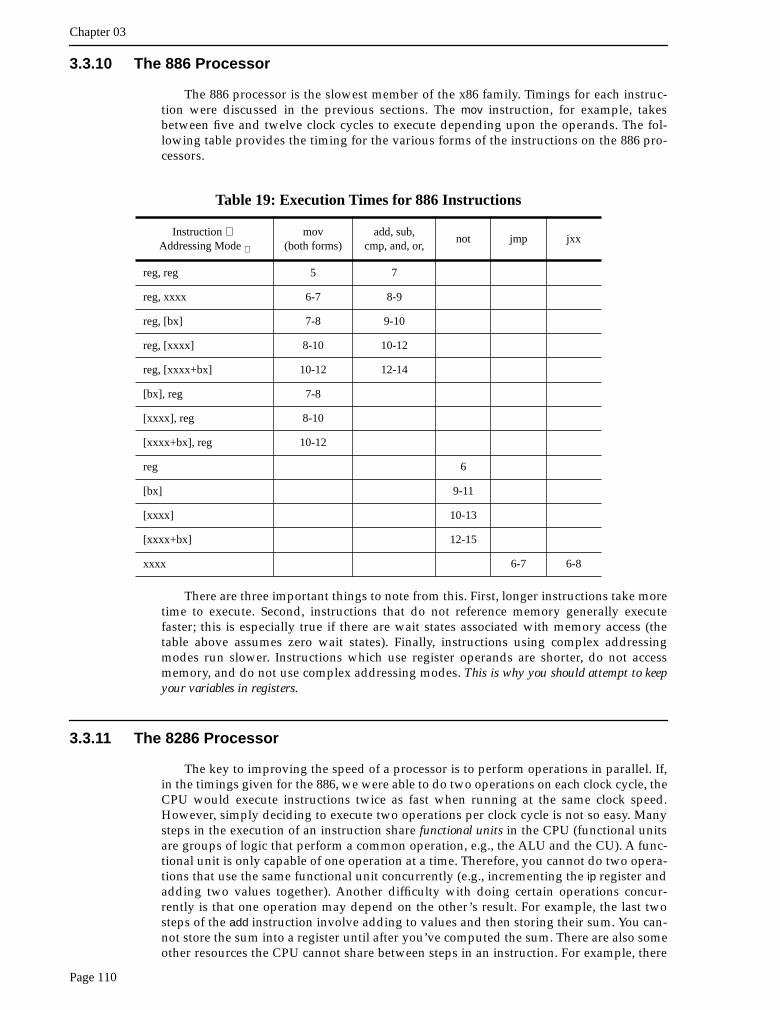
Chapter 03
Page 110
3.3.10 The 886 Processor
The 886 processor is the slowest member of the x86 family. Timings for each instruc-tion were discussed in the previous sections. The mov instruction, for example, takesbetween five and twelve clock cycles to execute depending upon the operands. The fol-lowing table provides the timing for the various forms of the instructions on the 886 pro-cessors.
There are three important things to note from this. First, longer instructions take moretime to execute. Second, instructions that do not reference memory generally executefaster; this is especially true if there are wait states associated with memory access (thetable above assumes zero wait states). Finally, instructions using complex addressingmodes run slower. Instructions which use register operands are shorter, do not accessmemory, and do not use complex addressing modes. This is why you should attempt to keepyour variables in registers.
3.3.11 The 8286 Processor
The key to improving the speed of a processor is to perform operations in parallel. If,in the timings given for the 886, we were able to do two operations on each clock cycle, theCPU would execute instructions twice as fast when running at the same clock speed.However, simply deciding to execute two operations per clock cycle is not so easy. Manysteps in the execution of an instruction share functional units in the CPU (functional unitsare groups of logic that perform a common operation, e.g., the ALU and the CU). A func-tional unit is only capable of one operation at a time. Therefore, you cannot do two opera-tions that use the same functional unit concurrently (e.g., incrementing the ip register andadding two values together). Another difficulty with doing certain operations concur-rently is that one operation may depend on the other’s result. For example, the last twosteps of the add instruction involve adding to values and then storing their sum. You can-not store the sum into a register until after you’ve computed the sum. There are also someother resources the CPU cannot share between steps in an instruction. For example, there
Table 19: Execution Times for 886 Instructions
Instruction ⇒Addressing Mode ⇓
mov (both forms)
add, sub, cmp, and, or,
not jmp jxx
reg, reg 5 7
reg, xxxx 6-7 8-9
reg, [bx] 7-8 9-10
reg, [xxxx] 8-10 10-12
reg, [xxxx+bx] 10-12 12-14
[bx], reg 7-8
[xxxx], reg 8-10
[xxxx+bx], reg 10-12
reg 6
[bx] 9-11
[xxxx] 10-13
[xxxx+bx] 12-15
xxxx 6-7 6-8
System Organization
Page 111
is only one data bus; the CPU cannot fetch an instruction opcode at the same time it is try-ing to store some data to memory. The trick in designing a CPU that executes several stepsin parallel is to arrange those steps to reduce conflicts or add additional logic so the two(or more) operations can occur simultaneously by executing in different functional units.
Consider again the steps the mov reg, mem/reg/const instruction requires:
• Fetch the instruction byte from memory.• Update the ip register to point at the next byte.• Decode the instruction to see what it does.• If required, fetch a 16-bit instruction operand from memory.• If required, update ip to point beyond the operand.• Compute the address of the operand, if required (i.e., bx+xxxx) .• Fetch the operand.• Store the fetched value into the destination register
The first operation uses the value of the ip register (so we cannot overlap incrementingip with it) and it uses the bus to fetch the instruction opcode from memory. Every step thatfollows this one depends upon the opcode it fetches from memory, so it is unlikely we willbe able to overlap the execution of this step with any other.
The second and third operations do not share any functional units, nor does decodingan opcode depend upon the value of the ip register. Therefore, we can easily modify thecontrol unit so that it increments the ip register at the same time it decodes the instruction.This will shave one cycle off the execution of the mov instruction.
The third and fourth operations above (decoding and optionally fetching the 16-bitoperand) do not look like they can be done in parallel since you must decode the instruc-tion to determine if it the CPU needs to fetch a 16-bit operand from memory. However, wecould design the CPU to go ahead and fetch the operand anyway, so that it’s available ifwe need it. There is one problem with this idea, though, we must have the address of theoperand to fetch (the value in the ip register) and if we must wait until we are done incre-menting the ip register before fetching this operand. If we are incrementing ip at the sametime we’re decoding the instruction, we will have to wait until the next cycle to fetch thisoperand.
Since the next three steps are optional, there are several possible instruction sequencesat this point:
#1 (step 4, step 5, step 6, and step 7) – e.g., mov ax, [1000+bx]
#2 (step 4, step 5, and step 7) – e.g., mov ax, [1000]
#3 (step 6 and step 7) – e.g., mov ax, [bx]
#4 (step 7) – e.g., mov ax, bx
In the sequences above, step seven always relies on the previous set in the sequence.Therefore, step seven cannot execute in parallel with any of the other steps. Step six alsorelies upon step four. Step five cannot execute in parallel with step four since step fouruses the value in the ip register, however, step five can execute in parallel with any otherstep. Therefore, we can shave one cycle off the first two sequences above as follows:
#1 (step 4, step 5/6, and step 7)
#2 (step 4, step 5/7)
#3 (step 6 and step 7)
#4 (step 7)
Of course, there is no way to overlap the execution of steps seven and eight in the movinstruction since it must surely fetch the value before storing it away. By combining thesesteps, we obtain the following steps for the mov instruction:
• Fetch the instruction byte from memory.• Decode the instruction and update ip• If required, fetch a 16-bit instruction operand from memory.• Compute the address of the operand, if required (i.e., bx+xxxx) .• Fetch the operand, if required update ip to point beyond xxxx.
Chapter 03
Page 112
• Store the fetched value into the destination register
By adding a small amount of logic to the CPU, we’ve shaved one or two cycles off theexecution of the mov instruction. This simple optimization works with most of the otherinstructions as well.
Another problem with the execution of the mov instruction concerns opcode align-ment. Consider the mov ax, [1000] instruction that appears at location 100 in memory. TheCPU spends one cycle fetching the opcode and, after decoding the instruction an deter-mining it has a 16-bit operand, it takes two additional cycles to fetch that operand frommemory (because that operand appears at an odd address – 101). The real travesty here isthat the extra clock cycle to fetch these two bytes is unnecessary, after all, the CPU fetchedthe L.O. byte of the operand when it grabbed the opcode (remember, the x86 CPUs are16-bit processors and always fetch 16 bits from memory), why not save that byte and useonly one additional clock cycle to fetch the H.O. byte? This would shave one cycle off theexecution time when the instruction begins at an even address (so the operand falls on anodd address). It would require only a one-byte register and a small amount of additionallogic to accomplish this, well worth the effort.
While we are adding a register to buffer up operand bytes, let’s consider some addi-tional optimizations that could use the same logic. For example, consider what happenswith that same mov instruction above executes. If we fetch the opcode and L.O. operandbyte on the first cycle and the H.O. byte of the operand on the second cycle, we’ve actuallyread four bytes, not three. That fourth byte is the opcode of the next instruction. If wecould save this opcode until the execution of the next instruction, we could shave a cycleof its execution time since it would not have to fetch the opcode byte. Furthermore, sincethe instruction decoder is idle while the CPU is executing the mov instruction, we canactually decode the next instruction while the current instruction is executing, therebyshaving yet another cycle off the execution of the next instruction. On the average, we willfetch this extra byte on every other instruction. Therefore, implementing this simplescheme will allow us to shave two cycles off about 50% of the instructions we execute.
Can we do anything about the other 50% of the instructions? The answer is yes. Notethat the execution of the mov instruction is not accessing memory on every clock cycle.For example, while storing the data into the destination register the bus is idle. Duringtime periods when the bus is idle we can pre-fetch instruction opcodes and operands andsave these values for executing the next instruction.
The major improvement to the 8286 over the 886 processor is the prefetch queue. When-ever the CPU is not using the Bus Interface Unit (BIU), the BIU can fetch additional bytesfrom the instruction stream. Whenever the CPU needs an instruction or operand byte, itgrabs the next available byte from the prefetch queue. Since the BIU grabs two bytes at atime from memory at one shot and the CPU generally consumes fewer than two bytes perclock cycle, any bytes the CPU would normally fetch from the instruction stream willalready be sitting in the prefetch queue.
Note, however, that we’re not guaranteed that all instructions and operands will besitting in the prefetch queue when we need them. For example, the jmp 1000 instructionwill invalidate the contents of the prefetch queue. If this instruction appears at location400, 401, and 402 in memory, the prefetch queue will contain the bytes at addresses 403,404, 405, 406, 407, etc. After loading ip with 1000 the bytes at addresses 403, etc., won’t dous any good. So the system has to pause for a moment to fetch the double word at address1000 before it can go on.
Another improvement we can make is to overlap instruction decoding with the laststep of the previous instruction. After the CPU processes the operand, the next availablebyte in the prefetch queue is an opcode, and the CPU can decode it in anticipation of itsexecution. Of course, if the current instruction modifies the ip register, any time spentdecoding the next instruction goes to waste, but since this occurs in parallel with otheroperations, it does not slow down the system.
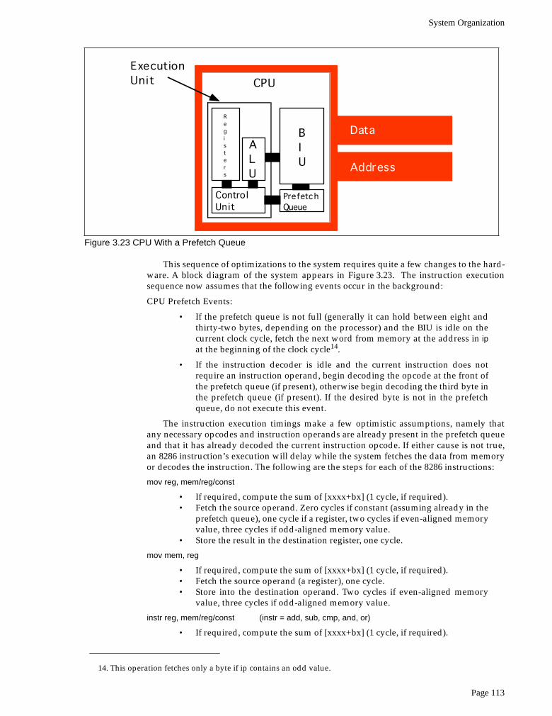
System Organization
Page 113
This sequence of optimizations to the system requires quite a few changes to the hard-ware. A block diagram of the system appears in Figure 3.23. The instruction executionsequence now assumes that the following events occur in the background:
CPU Prefetch Events:
• If the prefetch queue is not full (generally it can hold between eight andthirty-two bytes, depending on the processor) and the BIU is idle on thecurrent clock cycle, fetch the next word from memory at the address in ipat the beginning of the clock cycle14.
• If the instruction decoder is idle and the current instruction does notrequire an instruction operand, begin decoding the opcode at the front ofthe prefetch queue (if present), otherwise begin decoding the third byte inthe prefetch queue (if present). If the desired byte is not in the prefetchqueue, do not execute this event.
The instruction execution timings make a few optimistic assumptions, namely thatany necessary opcodes and instruction operands are already present in the prefetch queueand that it has already decoded the current instruction opcode. If either cause is not true,an 8286 instruction’s execution will delay while the system fetches the data from memoryor decodes the instruction. The following are the steps for each of the 8286 instructions:
mov reg, mem/reg/const
• If required, compute the sum of [xxxx+bx] (1 cycle, if required).• Fetch the source operand. Zero cycles if constant (assuming already in the
prefetch queue), one cycle if a register, two cycles if even-aligned memoryvalue, three cycles if odd-aligned memory value.
• Store the result in the destination register, one cycle.
mov mem, reg
• If required, compute the sum of [xxxx+bx] (1 cycle, if required).• Fetch the source operand (a register), one cycle.• Store into the destination operand. Two cycles if even-aligned memory
value, three cycles if odd-aligned memory value.
instr reg, mem/reg/const (instr = add, sub, cmp, and, or)
• If required, compute the sum of [xxxx+bx] (1 cycle, if required).
14. This operation fetches only a byte if ip contains an odd value.
Figure 3.23 CPU With a Prefetch Queue
CPU
BIU
ControlUnit
PrefetchQueue
ALU
Registers
Data
Address
ExecutionUnit
Chapter 03
Page 114
• Fetch the source operand. Zero cycles if constant (assuming already in theprefetch queue), one cycle if a register, two cycles if even-aligned memoryvalue, three cycles if odd-aligned memory value.
• Fetch the value of the first operand (a register), one cycle.• Compute the sum, difference, etc., as appropriate, one cycle.• Store the result in the destination register, one cycle.
not mem/reg
• If required, compute the sum of [xxxx+bx] (1 cycle, if required).• Fetch the source operand. One cycle if a register, two cycles if
even-aligned memory value, three cycles if odd-aligned memory value.• Logically not the value, one cycle.• Store the result, one cycle if a register, two cycles if even-aligned memory
value, three cycles if odd-aligned memory value.
jcc xxxx (conditional jump, cc=a, ae, b, be, e, ne)
• Test the current condition code (less than and equal) flags, one cycle.• If the flag values are appropriate for the particular conditional branch, the
CPU copies the 16-bit instruction operand into the ip register, one cycle.
jmp xxxx
• The CPU copies the 16-bit instruction operand into the ip register, onecycle.
As for the 886, we will not consider the execution times of the other x86 instructions sincemost of them are indeterminate.
The jump instructions look like they execute very quickly on the 8286. In fact, theymay execute very slowly. Don’t forget, jumping from one location to another invalidatesthe contents of the prefetch queue. So although the jmp instruction looks like it executes inone clock cycle, it forces the CPU to flush the prefetch queue and, therefore, spend severalcycles fetching the next instruction, fetching additional operands, and decoding thatinstruction. Indeed, it make be two or three instructions after the jmp instruction beforethe CPU is back to the point where the prefetch queue is operating smoothly and the CPUis decoding opcodes in parallel with the execution of the previous instruction. The has onevery important implication to your programs: if you want to write fast code, make sure toavoid jumping around in your program as much as possible.
Note that the conditional jump instructions only invalidate the prefetch queue if theyactually make the jump. If the condition is false, they fall through to the next instructionand continue to use the values in the prefetch queue as well as any pre-decoded instruc-tion opcodes. Therefore, if you can determine, while writing the program, which condi-tion is most likely (e.g., less than vs. not less than), you should arrange your program sothat the most common case falls through and conditional jump rather than take thebranch.
Instruction size (in bytes) can also affect the performance of the prefetch queue. Itnever requires more than one clock cycle to fetch a single byte instruction, but it alwaysrequires two cycles to fetch a three-byte instruction. Therefore, if the target of a jumpinstruction is two one-byte instructions, the BIU can fetch both instructions in one clockcycle and begin decoding the second one while executing the first. If these instructions arethree-byte instructions, the CPU may not have enough time to fetch and decode the sec-ond or third instruction by the time it finishes the first. Therefore, you should attempt touse shorter instructions whenever possible since they will improve the performance of theprefetch queue.
The following table provides the (optimistic) execution times for the 8286 instructions:
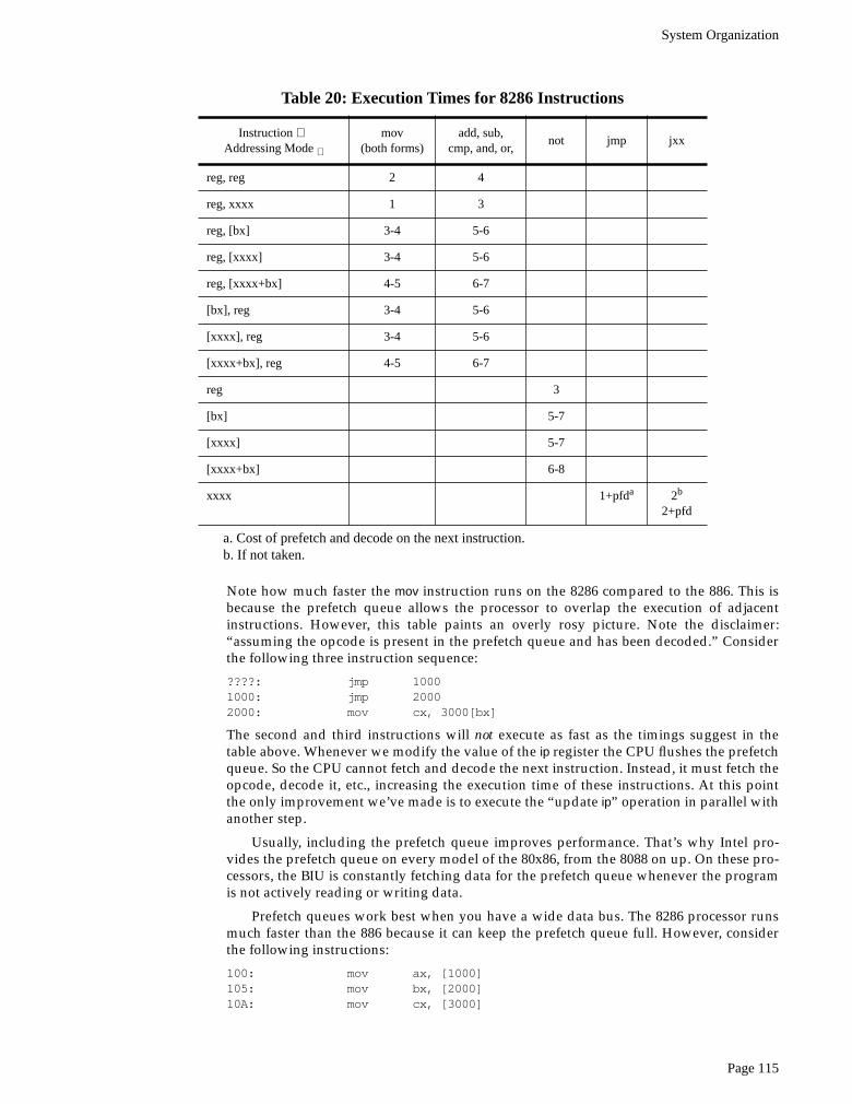
System Organization
Page 115
Note how much faster the mov instruction runs on the 8286 compared to the 886. This isbecause the prefetch queue allows the processor to overlap the execution of adjacentinstructions. However, this table paints an overly rosy picture. Note the disclaimer:“assuming the opcode is present in the prefetch queue and has been decoded.” Considerthe following three instruction sequence:
????: jmp 10001000: jmp 20002000: mov cx, 3000[bx]
The second and third instructions will not execute as fast as the timings suggest in thetable above. Whenever we modify the value of the ip register the CPU flushes the prefetchqueue. So the CPU cannot fetch and decode the next instruction. Instead, it must fetch theopcode, decode it, etc., increasing the execution time of these instructions. At this pointthe only improvement we’ve made is to execute the “update ip” operation in parallel withanother step.
Usually, including the prefetch queue improves performance. That’s why Intel pro-vides the prefetch queue on every model of the 80x86, from the 8088 on up. On these pro-cessors, the BIU is constantly fetching data for the prefetch queue whenever the programis not actively reading or writing data.
Prefetch queues work best when you have a wide data bus. The 8286 processor runsmuch faster than the 886 because it can keep the prefetch queue full. However, considerthe following instructions:
100: mov ax, [1000]105: mov bx, [2000]10A: mov cx, [3000]
a. Cost of prefetch and decode on the next instruction.b. If not taken.
Table 20: Execution Times for 8286 Instructions
Instruction ⇒Addressing Mode ⇓
mov (both forms)
add, sub, cmp, and, or,
not jmp jxx
reg, reg 2 4
reg, xxxx 1 3
reg, [bx] 3-4 5-6
reg, [xxxx] 3-4 5-6
reg, [xxxx+bx] 4-5 6-7
[bx], reg 3-4 5-6
[xxxx], reg 3-4 5-6
[xxxx+bx], reg 4-5 6-7
reg 3
[bx] 5-7
[xxxx] 5-7
[xxxx+bx] 6-8
xxxx 1+pfda 2b
2+pfd
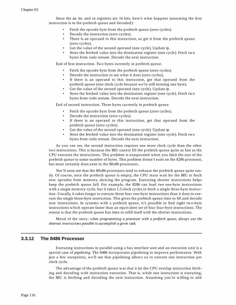
Chapter 03
Page 116
Since the ax, bx, and cx registers are 16 bits, here’s what happens (assuming the firstinstruction is in the prefetch queue and decoded):
• Fetch the opcode byte from the prefetch queue (zero cycles).• Decode the instruction (zero cycles). • There is an operand to this instruction, so get it from the prefetch queue
(zero cycles).• Get the value of the second operand (one cycle). Update ip.• Store the fetched value into the destination register (one cycle). Fetch two
bytes from code stream. Decode the next instruction.
End of first instruction. Two bytes currently in prefetch queue.
• Fetch the opcode byte from the prefetch queue (zero cycles).• Decode the instruction to see what it does (zero cycles). • If there is an operand to this instruction, get that operand from the
prefetch queue (one clock cycle because we’re still missing one byte).• Get the value of the second operand (one cycle). Update ip. • Store the fetched value into the destination register (one cycle). Fetch two
bytes from code stream. Decode the next instruction.
End of second instruction. Three bytes currently in prefetch queue.
• Fetch the opcode byte from the prefetch queue (zero cycles).• Decode the instruction (zero cycles). • If there is an operand to this instruction, get that operand from the
prefetch queue (zero cycles).• Get the value of the second operand (one cycle). Update ip. • Store the fetched value into the destination register (one cycle). Fetch two
bytes from code stream. Decode the next instruction.
As you can see, the second instruction requires one more clock cycle than the othertwo instructions. This is because the BIU cannot fill the prefetch queue quite as fast as theCPU executes the instructions. This problem is exasperated when you limit the size of theprefetch queue to some number of bytes. This problem doesn’t exist on the 8286 processor,but most certainly does exist in the 80x86 processors.
You’ll soon see that the 80x86 processors tend to exhaust the prefetch queue quite eas-ily. Of course, once the prefetch queue is empty, the CPU must wait for the BIU to fetchnew opcodes from memory, slowing the program. Executing shorter instructions helpskeep the prefetch queue full. For example, the 8286 can load two one-byte instructionswith a single memory cycle, but it takes 1.5 clock cycles to fetch a single three-byte instruc-tion. Usually, it takes longer to execute those four one-byte instructions than it does to exe-cute the single three-byte instruction. This gives the prefetch queue time to fill and decodenew instructions. In systems with a prefetch queue, it’s possible to find eight two-byteinstructions which operate faster than an equivalent set of four four-byte instructions. Thereason is that the prefetch queue has time to refill itself with the shorter instructions.
Moral of the story: when programming a processor with a prefetch queue, always use theshortest instructions possible to accomplish a given task.
3.3.12 The 8486 Processor
Executing instructions in parallel using a bus interface unit and an execution unit is aspecial case of pipelining. The 8486 incorporates pipelining to improve performance. Withjust a few exceptions, we’ll see that pipelining allows us to execute one instruction perclock cycle.
The advantage of the prefetch queue was that it let the CPU overlap instruction fetch-ing and decoding with instruction execution. That is, while one instruction is executing,the BIU is fetching and decoding the next instruction. Assuming you’re willing to add
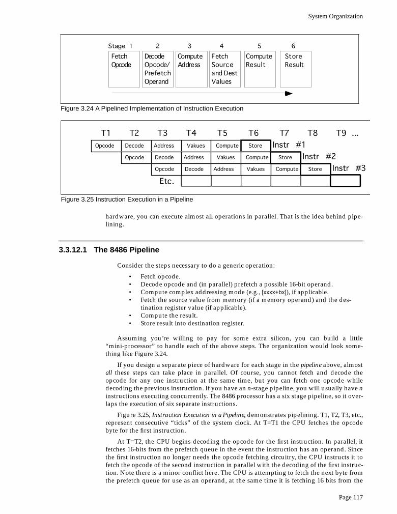
System Organization
Page 117
hardware, you can execute almost all operations in parallel. That is the idea behind pipe-lining.
3.3.12.1 The 8486 Pipeline
Consider the steps necessary to do a generic operation:
• Fetch opcode.• Decode opcode and (in parallel) prefetch a possible 16-bit operand.• Compute complex addressing mode (e.g., [xxxx+bx]), if applicable.• Fetch the source value from memory (if a memory operand) and the des-
tination register value (if applicable).• Compute the result.• Store result into destination register.
Assuming you’re willing to pay for some extra silicon, you can build a little“mini-processor” to handle each of the above steps. The organization would look some-thing like Figure 3.24.
If you design a separate piece of hardware for each stage in the pipeline above, almostall these steps can take place in parallel. Of course, you cannot fetch and decode theopcode for any one instruction at the same time, but you can fetch one opcode whiledecoding the previous instruction. If you have an n-stage pipeline, you will usually have ninstructions executing concurrently. The 8486 processor has a six stage pipeline, so it over-laps the execution of six separate instructions.
Figure 3.25, Instruction Execution in a Pipeline, demonstrates pipelining. T1, T2, T3, etc.,represent consecutive “ticks” of the system clock. At T=T1 the CPU fetches the opcodebyte for the first instruction.
At T=T2, the CPU begins decoding the opcode for the first instruction. In parallel, itfetches 16-bits from the prefetch queue in the event the instruction has an operand. Sincethe first instruction no longer needs the opcode fetching circuitry, the CPU instructs it tofetch the opcode of the second instruction in parallel with the decoding of the first instruc-tion. Note there is a minor conflict here. The CPU is attempting to fetch the next byte fromthe prefetch queue for use as an operand, at the same time it is fetching 16 bits from the
Figure 3.24 A Pipelined Implementation of Instruction Execution
FetchOpcode
DecodeOpcode /PrefetchOperand
ComputeAddress
FetchSourceand DestValues
ComputeResult
StoreResult
Stage 1 2 3 4 5 6
Figure 3.25 Instruction Execution in a Pipeline
DecodeOpcode Address Vakues Compute Store
T1 T2 T3 T4 T5 T6 T7 T8 T9 ...
Etc.
Instr #1
Instr #2
Instr #3
DecodeOpcode Address Vakues Compute
DecodeOpcode Address Vakues Compute
Store
Store
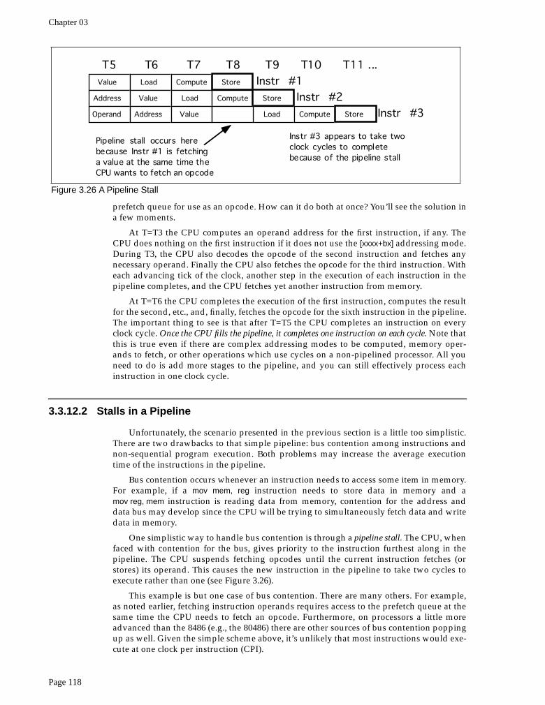
Chapter 03
Page 118
prefetch queue for use as an opcode. How can it do both at once? You’ll see the solution ina few moments.
At T=T3 the CPU computes an operand address for the first instruction, if any. TheCPU does nothing on the first instruction if it does not use the [xxxx+bx] addressing mode.During T3, the CPU also decodes the opcode of the second instruction and fetches anynecessary operand. Finally the CPU also fetches the opcode for the third instruction. Witheach advancing tick of the clock, another step in the execution of each instruction in thepipeline completes, and the CPU fetches yet another instruction from memory.
At T=T6 the CPU completes the execution of the first instruction, computes the resultfor the second, etc., and, finally, fetches the opcode for the sixth instruction in the pipeline.The important thing to see is that after T=T5 the CPU completes an instruction on everyclock cycle. Once the CPU fills the pipeline, it completes one instruction on each cycle. Note thatthis is true even if there are complex addressing modes to be computed, memory oper-ands to fetch, or other operations which use cycles on a non-pipelined processor. All youneed to do is add more stages to the pipeline, and you can still effectively process eachinstruction in one clock cycle.
3.3.12.2 Stalls in a Pipeline
Unfortunately, the scenario presented in the previous section is a little too simplistic.There are two drawbacks to that simple pipeline: bus contention among instructions andnon-sequential program execution. Both problems may increase the average executiontime of the instructions in the pipeline.
Bus contention occurs whenever an instruction needs to access some item in memory.For example, if a mov mem, reg instruction needs to store data in memory and amov reg, mem instruction is reading data from memory, contention for the address anddata bus may develop since the CPU will be trying to simultaneously fetch data and writedata in memory.
One simplistic way to handle bus contention is through a pipeline stall. The CPU, whenfaced with contention for the bus, gives priority to the instruction furthest along in thepipeline. The CPU suspends fetching opcodes until the current instruction fetches (orstores) its operand. This causes the new instruction in the pipeline to take two cycles toexecute rather than one (see Figure 3.26).
This example is but one case of bus contention. There are many others. For example,as noted earlier, fetching instruction operands requires access to the prefetch queue at thesame time the CPU needs to fetch an opcode. Furthermore, on processors a little moreadvanced than the 8486 (e.g., the 80486) there are other sources of bus contention poppingup as well. Given the simple scheme above, it’s unlikely that most instructions would exe-cute at one clock per instruction (CPI).
Figure 3.26 A Pipeline Stall
Value Load Compute Store
T5 T6 T7 T8 T9 T10 T11 ...
Address Value Load Compute Store
Operand Address Value Load Compute Store
Instr #1
Instr #2
Instr #3
Pipeline stall occurs herebecause Instr #1 is fetchinga value at the same time theCPU wants to fetch an opcode
Instr #3 appears to take twoclock cycles to completebecause of the pipeline stall
System Organization
Page 119
Fortunately, the intelligent use of a cache system can eliminate many pipeline stallslike the ones discussed above. The next section on caching will describe how this is done.However, it is not always possible, even with a cache, to avoid stalling the pipeline. Whatyou cannot fix in hardware, you can take care of with software. If you avoid using mem-ory, you can reduce bus contention and your programs will execute faster. Likewise, usingshorter instructions also reduces bus contention and the possibility of a pipeline stall.
What happens when an instruction modifies the ip register? By the time the instruction
jmp 1000
completes execution, we’ve already started five other instructions and we’re only oneclock cycle away from the completion of the first of these. Obviously, the CPU must notexecute those instructions or it will compute improper results.
The only reasonable solution is to flush the entire pipeline and begin fetching opcodesanew. However, doing so causes a severe execution time penalty. It will take six clockcycles (the length of the 8486 pipeline) before the next instruction completes execution.Clearly, you should avoid the use of instructions which interrupt the sequential executionof a program. This also shows another problem – pipeline length. The longer the pipelineis, the more you can accomplish per cycle in the system. However, lengthening a pipelinemay slow a program if it jumps around quite a bit. Unfortunately, you cannot control thenumber of stages in the pipeline. You can, however, control the number of transfer instruc-tions which appear in your programs. Obviously you should keep these to a minimum ina pipelined system.
3.3.12.3 Cache, the Prefetch Queue, and the 8486
System designers can resolve many problems with bus contention through the intelli-gent use of the prefetch queue and the cache memory subsystem. They can design theprefetch queue to buffer up data from the instruction stream, and they can design thecache with separate data and code areas. Both techniques can improve system perfor-mance by eliminating some conflicts for the bus.
The prefetch queue simply acts as a buffer between the instruction stream in memoryand the opcode fetching circuitry. Unfortunately, the prefetch queue on the 8486 does notenjoy the advantage it had on the 8286. The prefetch queue works well for the 8286because the CPU isn’t constantly accessing memory. When the CPU isn’t accessing mem-ory, the BIU can fetch additional instruction opcodes for the prefetch queue. Alas, the 8486CPU is constantly accessing memory since it fetches an opcode byte on every clock cycle.Therefore, the prefetch queue cannot take advantage of any “dead” bus cycles to fetchadditional opcode bytes – there aren’t any “dead” bus cycles. However, the prefetchqueue is still valuable on the 8486 for a very simple reason: the BIU fetches two bytes oneach memory access, yet some instructions are only one byte long. Without the prefetchqueue, the system would have to explicitly fetch each opcode, even if the BIU had already“accidentally” fetched the opcode along with the previous instruction. With the prefetchqueue, however, the system will not refetch any opcodes. It fetches them once and savesthem for use by the opcode fetch unit.
For example, if you execute two one-byte instructions in a row, the BIU can fetch bothopcodes in one memory cycle, freeing up the bus for other operations. The CPU can usethese available bus cycles to fetch additional opcodes or to deal with other memoryaccesses.
Of course, not all instructions are one byte long. The 8486 has two instruction sizes:one byte and three bytes. If you execute several three-byte load instructions in a row,you’re going to run slower, e.g.,
mov ax, 1000mov bx, 2000mov cx, 3000add ax, 5000

Chapter 03
Page 120
Each of these instructions reads an opcode byte and a 16 bit operand (the constant).Therefore, it takes an average of 1.5 clock cycles to read each instruction above. As a result,the instructions will require six clock cycles to execute rather than four.
Once again we return to that same rule: the fastest programs are the ones which use theshortest instructions. If you can use shorter instructions to accomplish some task, do so. Thefollowing instruction sequence provides a good example:
mov ax, 1000mov bx, 1000mov cx, 1000add ax, 1000
We can reduce the size of this program and increase its execution speed by changing it to:
mov ax, 1000mov bx, axmov cx, axadd ax, ax
This code is only five bytes long compared to 12 bytes for the previous example. Theprevious code will take a minimum of five clock cycles to execute, more if there are otherbus contention problems. The latter example takes only four15. Furthermore, the secondexample leaves the bus free for three of those four clock periods, so the BIU can load addi-tional opcodes. Remember, shorter often means faster.
While the prefetch queue can free up bus cycles and eliminate bus contention, someproblems still exist. Suppose the average instruction length for a sequence of instructionsis 2.5 bytes (achieved by having three three-byte instructions and one one-byte instructiontogether). In such a case the bus will be kept busy fetching opcodes and instruction oper-ands. There will be no free time left to access memory. Assuming some of those instruc-tions access memory the pipeline will stall, slowing execution.
Suppose, for a moment, that the CPU has two separate memory spaces, one forinstructions and one for data, each with their own bus. This is called the Harvard Archi-tecture since the first such machine was built at Harvard. On a Harvard machine therewould be no contention for the bus. The BIU could continue to fetch opcodes on theinstruction bus while accessing memory on the data/memory bus (see Figure 3.27),
15. Actually, both of these examples will take longer to execute. See the section on hazards for more details.
Figure 3.27 A Typical Harvard Machine
CPU
Data Memory
I/O Devices
Data/Memory Bus
Instruction Bus Instruction Memory
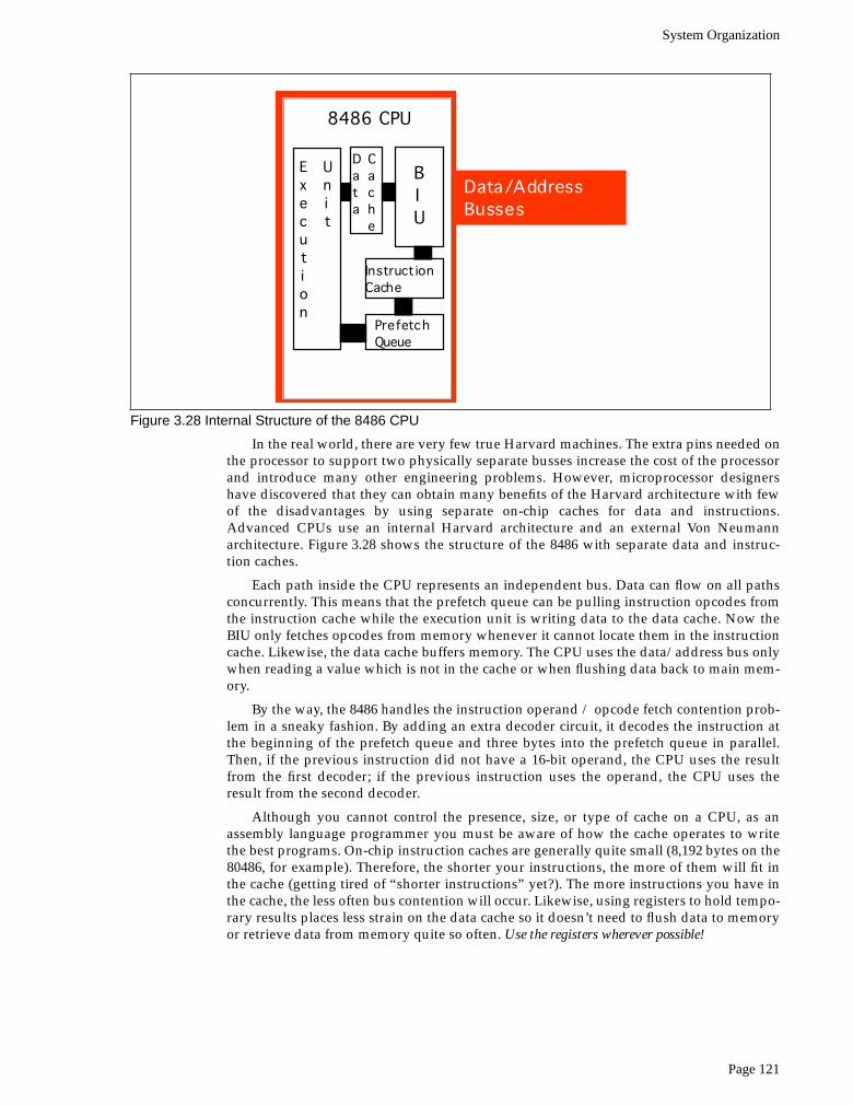
System Organization
Page 121
In the real world, there are very few true Harvard machines. The extra pins needed onthe processor to support two physically separate busses increase the cost of the processorand introduce many other engineering problems. However, microprocessor designershave discovered that they can obtain many benefits of the Harvard architecture with fewof the disadvantages by using separate on-chip caches for data and instructions.Advanced CPUs use an internal Harvard architecture and an external Von Neumannarchitecture. Figure 3.28 shows the structure of the 8486 with separate data and instruc-tion caches.
Each path inside the CPU represents an independent bus. Data can flow on all pathsconcurrently. This means that the prefetch queue can be pulling instruction opcodes fromthe instruction cache while the execution unit is writing data to the data cache. Now theBIU only fetches opcodes from memory whenever it cannot locate them in the instructioncache. Likewise, the data cache buffers memory. The CPU uses the data/address bus onlywhen reading a value which is not in the cache or when flushing data back to main mem-ory.
By the way, the 8486 handles the instruction operand / opcode fetch contention prob-lem in a sneaky fashion. By adding an extra decoder circuit, it decodes the instruction atthe beginning of the prefetch queue and three bytes into the prefetch queue in parallel.Then, if the previous instruction did not have a 16-bit operand, the CPU uses the resultfrom the first decoder; if the previous instruction uses the operand, the CPU uses theresult from the second decoder.
Although you cannot control the presence, size, or type of cache on a CPU, as anassembly language programmer you must be aware of how the cache operates to writethe best programs. On-chip instruction caches are generally quite small (8,192 bytes on the80486, for example). Therefore, the shorter your instructions, the more of them will fit inthe cache (getting tired of “shorter instructions” yet?). The more instructions you have inthe cache, the less often bus contention will occur. Likewise, using registers to hold tempo-rary results places less strain on the data cache so it doesn’t need to flush data to memoryor retrieve data from memory quite so often. Use the registers wherever possible!
Figure 3.28 Internal Structure of the 8486 CPU
8486 CPU
BIU
Data/AddressBusses
Instruct ionCache
PrefetchQueue
Data
Cache
Execution
Unit
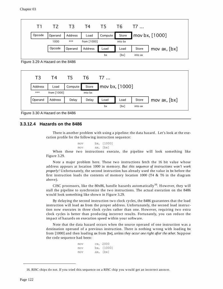
Chapter 03
Page 122
3.3.12.4 Hazards on the 8486
There is another problem with using a pipeline: the data hazard. Let’s look at the exe-cution profile for the following instruction sequence:
mov bx, [1000]mov ax, [bx]
When these two instructions execute, the pipeline will look something likeFigure 3.29.
Note a major problem here. These two instructions fetch the 16 bit value whoseaddress appears at location 1000 in memory. But this sequence of instructions won’t workproperly! Unfortunately, the second instruction has already used the value in bx before thefirst instruction loads the contents of memory location 1000 (T4 & T6 in the diagramabove).
CISC processors, like the 80x86, handle hazards automatically16. However, they willstall the pipeline to synchronize the two instructions. The actual execution on the 8486would look something like shown in Figure 3.29.
By delaying the second instruction two clock cycles, the 8486 guarantees that the loadinstruction will load ax from the proper address. Unfortunately, the second load instruc-tion now executes in three clock cycles rather than one. However, requiring two extraclock cycles is better than producing incorrect results. Fortunately, you can reduce theimpact of hazards on execution speed within your software.
Note that the data hazard occurs when the source operand of one instruction was adestination operand of a previous instruction. There is nothing wrong with loading bxfrom [1000] and then loading ax from [bx], unless they occur one right after the other. Supposethe code sequence had been:
mov cx, 2000mov bx, [1000]mov ax, [bx]
16. RISC chips do not. If you tried this sequence on a RISC chip you would get an incorrect answer.
Figure 3.29 A Hazard on the 8486
into bx
T1 T2 T3 T4 T5 T6 T7 ...
Operand Address Store mov bx, [1000]
mov ax, [bx]
Opcode
Operand Load Load StoreOpcode
1000 ***
bx [bx] into ax
from [1000]
Load Compute
Address
Figure 3.30 A Hazard on the 8486
into bx
T3 T4 T5 T6 T7 ...
Address Store mov bx, [1000]
mov ax, [bx]Operand Load Load Store
***
bx [bx] into ax
from [1000]
Load Compute
Address Delay Delay
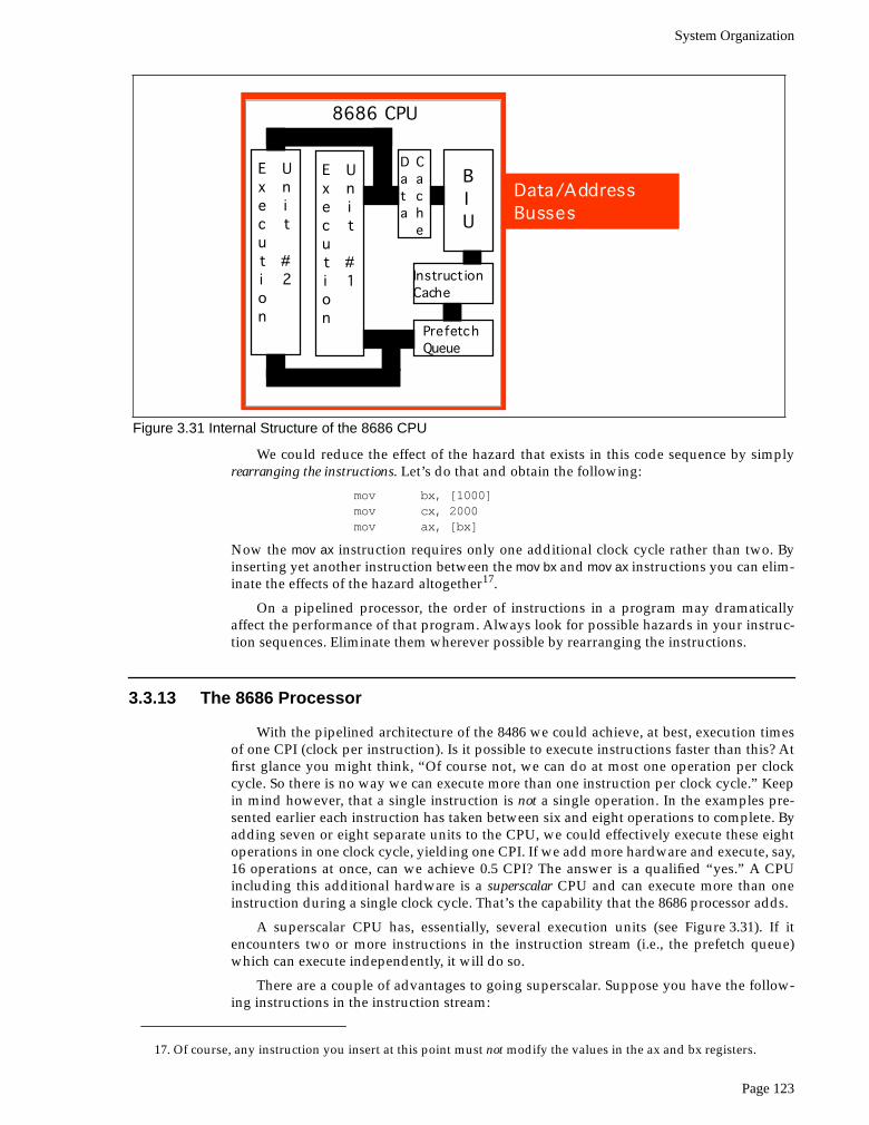
System Organization
Page 123
We could reduce the effect of the hazard that exists in this code sequence by simplyrearranging the instructions. Let’s do that and obtain the following:
mov bx, [1000]mov cx, 2000mov ax, [bx]
Now the mov ax instruction requires only one additional clock cycle rather than two. Byinserting yet another instruction between the mov bx and mov ax instructions you can elim-inate the effects of the hazard altogether17.
On a pipelined processor, the order of instructions in a program may dramaticallyaffect the performance of that program. Always look for possible hazards in your instruc-tion sequences. Eliminate them wherever possible by rearranging the instructions.
3.3.13 The 8686 Processor
With the pipelined architecture of the 8486 we could achieve, at best, execution timesof one CPI (clock per instruction). Is it possible to execute instructions faster than this? Atfirst glance you might think, “Of course not, we can do at most one operation per clockcycle. So there is no way we can execute more than one instruction per clock cycle.” Keepin mind however, that a single instruction is not a single operation. In the examples pre-sented earlier each instruction has taken between six and eight operations to complete. Byadding seven or eight separate units to the CPU, we could effectively execute these eightoperations in one clock cycle, yielding one CPI. If we add more hardware and execute, say,16 operations at once, can we achieve 0.5 CPI? The answer is a qualified “yes.” A CPUincluding this additional hardware is a superscalar CPU and can execute more than oneinstruction during a single clock cycle. That’s the capability that the 8686 processor adds.
A superscalar CPU has, essentially, several execution units (see Figure 3.31). If itencounters two or more instructions in the instruction stream (i.e., the prefetch queue)which can execute independently, it will do so.
There are a couple of advantages to going superscalar. Suppose you have the follow-ing instructions in the instruction stream:
17. Of course, any instruction you insert at this point must not modify the values in the ax and bx registers.
Figure 3.31 Internal Structure of the 8686 CPU
8686 CPU
BIU
Data/AddressBusses
Instruct ionCache
PrefetchQueue
Data
Cache
Execution
Unit
#1
Execution
Unit
#2

Chapter 03
Page 124
mov ax, 1000mov bx, 2000
If there are no other problems or hazards in the surrounding code, and all six bytes forthese two instructions are currently in the prefetch queue, there is no reason why the CPUcannot fetch and execute both instructions in parallel. All it takes is extra silicon on theCPU chip to implement two execution units.
Besides speeding up independent instructions, a superscalar CPU can also speed upprogram sequences which have hazards. One limitation of the 8486 CPU is that once ahazard occurs, the offending instruction will completely stall the pipeline. Every instruc-tion which follows will also have to wait for the CPU to synchronize the execution of theinstructions. With a superscalar CPU, however, instructions following the hazard maycontinue execution through the pipeline as long as they don’t have hazards of their own.This alleviates (though does not eliminate) some of the need for careful instruction sched-uling.
As an assembly language programmer, the way you write software for a superscalarCPU can dramatically affect its performance. First and foremost is that rule you’re proba-bly sick of by now: use short instructions. The shorter your instructions are, the moreinstructions the CPU can fetch in a single operation and, therefore, the more likely theCPU will execute faster than one CPI. Most superscalar CPUs do not completely duplicatethe execution unit. There might be multiple ALUs, floating point units, etc. This meansthat certain instruction sequences can execute very quickly while others won’t. You haveto study the exact composition of your CPU to decide which instruction sequences pro-duce the best performance.
3.4 I/O (Input/Output)
There are three basic forms of input and output that a typical computer system willuse: I/O-mapped I/O, memory-mapped input/output, and direct memory access (DMA).I/O-mapped input/output uses special instructions to transfer data between the com-puter system and the outside world; memory-mapped I/O uses special memory locationsin the normal address space of the CPU to communicate with real-world devices; DMA isa special form of memory-mapped I/O where the peripheral device reads and writesmemory without going through the CPU. Each I/O mechanism has its own set of advan-tages and disadvantages, we will discuss these in this section.
The first thing to learn about the input/output subsystem is that I/O in a typical com-puter system is radically different than I/O in a typical high level programming language.In a real computer system you will rarely find machine instructions that behave likewriteln, printf, or even the x86 Get and Put instructions18. In fact, most input/outputinstructions behave exactly like the x86’s mov instruction. To send data to an outputdevice, the CPU simply moves that data to a special memory location (in the I/O addressspace if I/O-mapped input/output [see “The I/O Subsystem” on page 92] or to anaddress in the memory address space if using memory-mapped I/O). To read data froman input device, the CPU simply moves data from the address (I/O or memory) of thatdevice into the CPU. Other than there are usually more wait states associated with a typi-cal peripheral device than actual memory, the input or output operation looks very simi-lar to a memory read or write operation (see “Memory Access and the System Clock” onpage 93).
An I/O port is a device that looks like a memory cell to the computer but contains con-nections to the outside world. An I/O port typically uses a latch rather than a flip-flop toimplement the memory cell. When the CPU writes to the address associated with thelatch, the latch device captures the data and makes it available on a set of wires external tothe CPU and memory system (see Figure 3.32). Note that I/O ports can be read-only,write-only, or read/write. The port in Figure 3.32, for example, is a write-only port. Since
18. Get and Put behave the way they do in order to simplify writing x86 programs.
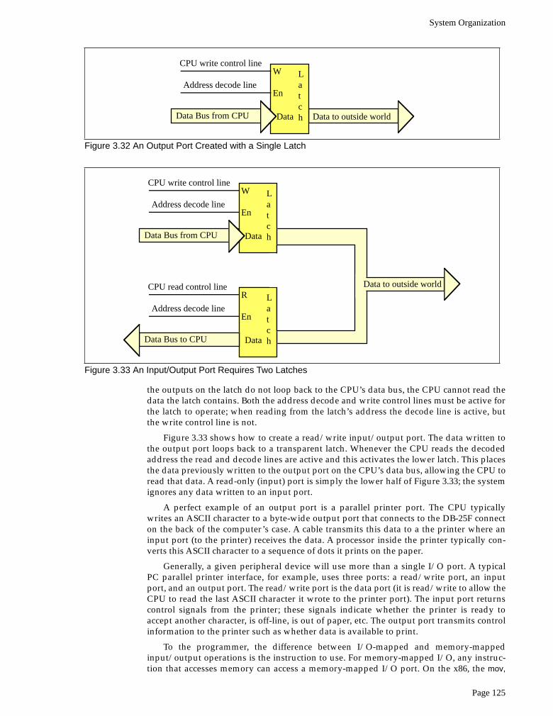
System Organization
Page 125
the outputs on the latch do not loop back to the CPU’s data bus, the CPU cannot read thedata the latch contains. Both the address decode and write control lines must be active forthe latch to operate; when reading from the latch’s address the decode line is active, butthe write control line is not.
Figure 3.33 shows how to create a read/write input/output port. The data written tothe output port loops back to a transparent latch. Whenever the CPU reads the decodedaddress the read and decode lines are active and this activates the lower latch. This placesthe data previously written to the output port on the CPU’s data bus, allowing the CPU toread that data. A read-only (input) port is simply the lower half of Figure 3.33; the systemignores any data written to an input port.
A perfect example of an output port is a parallel printer port. The CPU typicallywrites an ASCII character to a byte-wide output port that connects to the DB-25F connecton the back of the computer’s case. A cable transmits this data to a the printer where aninput port (to the printer) receives the data. A processor inside the printer typically con-verts this ASCII character to a sequence of dots it prints on the paper.
Generally, a given peripheral device will use more than a single I/O port. A typicalPC parallel printer interface, for example, uses three ports: a read/write port, an inputport, and an output port. The read/write port is the data port (it is read/write to allow theCPU to read the last ASCII character it wrote to the printer port). The input port returnscontrol signals from the printer; these signals indicate whether the printer is ready toaccept another character, is off-line, is out of paper, etc. The output port transmits controlinformation to the printer such as whether data is available to print.
To the programmer, the difference between I/O-mapped and memory-mappedinput/output operations is the instruction to use. For memory-mapped I/O, any instruc-tion that accesses memory can access a memory-mapped I/O port. On the x86, the mov,
Figure 3.32 An Output Port Created with a Single Latch
Data Bus from CPU
Latch
CPU write control line
Address decode line
W
En
Data Data to outside world
Figure 3.33 An Input/Output Port Requires Two Latches
Data Bus from CPU
Latch
CPU write control line
Address decode line
W
En
Data
Data Bus to CPU
Latch
CPU read control line
Address decode line
R
En
Data
Data to outside world
Chapter 03
Page 126
add, sub, cmp, and, or, and not instructions can read memory; the mov and not instructionscan write data to memory. I/O-mapped input/output uses special instructions to accessI/O ports. For example, the x86 CPUs use the get and put instructions19, the Intel 80x86family uses the in and out instructions. The 80x86 in and out instructions work just like themov instruction except they place their address on the I/O address bus rather than thememory address bus (See “The I/O Subsystem” on page 92.).
Memory-mapped I/O subsystems and I/O-mapped subsystems both require theCPU to move data between the peripheral device and main memory. For example, toinput a sequence of ten bytes from an input port and store these bytes into memory theCPU must read each value and store it into memory. For very high-speed I/O devices theCPU may be too slow when processing this data a byte at a time. Such devices generallycontain an interface to the CPU’s bus so it directly read and write memory. This is knownas direct memory access since the peripheral device accesses memory directly, without usingthe CPU as an intermediary. This often allows the I/O operation to proceed in parallelwith other CPU operations, thereby increasing the overall speed of the system. Note, how-ever, that the CPU and DMA device cannot both use the address and data busses at thesame time. Therefore, concurrent processing only occurs if the CPU has a cache and is exe-cuting code and accessing data found in the cache (so the bus is free). Nevertheless, even ifthe CPU must halt and wait for the DMA operation to complete, the I/O is still muchfaster since many of the bus operations during I/O or memory-mapped input/outputconsist of instruction fetches or I/O port accesses which are not present during DMAoperations.
3.5 Interrupts and Polled I/O
Many I/O devices cannot accept data at an arbitrary rate. For example, a Pentiumbased PC is capable of sending several million characters a second to a printer, but thatprinter is (probably) unable to print that many characters each second. Likewise, an inputdevice like a keyboard is unable to provide several million keystrokes per second (since itoperates at human speeds, not computer speeds). The CPU needs some mechanism tocoordinate data transfer between the computer system and its peripheral devices.
One common way to coordinate data transfer is to provide some status bits in a sec-ondary input port. For example, a one in a single bit in an I/O port can tell the CPU that aprinter is ready to accept more data, a zero would indicate that the printer is busy and theCPU should not send new data to the printer. Likewise, a one bit in a different port couldtell the CPU that a keystroke from the keyboard is available at the keyboard data port, azero in that same bit could indicate that no keystroke is available. The CPU can test thesebits prior to reading a key from the keyboard or writing a character to the printer.
Assume that the printer data port is memory-mapped to address 0FFE0h and theprinter status port is bit zero of memory-mapped port 0FFE2h. The following code waitsuntil the printer is ready to accept a byte of data and then it writes the byte in the L.O. byteof ax to the printer port:
0000: mov bx, [FFE2]0003: and bx, 10006: cmp bx, 00009: je 0000000C: mov [FFE0], ax
. . . . . .
The first instruction fetches the data at the status input port. The second instructionlogically ands this value with one to clear bits one through fifteen and set bit zero to thecurrent status of the printer port. Note that this produces the value zero in bx if the printer
19. Get and put are a little fancier than true I/O-mapped instructions, but we will ignore that difference here.

System Organization
Page 127
is busy, it produces the value one in bx if the printer is ready to accept additional data. Thethird instruction checks bx to see if it contains zero (i.e., the printer is busy). If the printer isbusy, this program jumps back to location zero and repeats this process over and overagain until the printer status bit is one20.
The following code provides an example of reading a keyboard. It presumes that thekeyboard status bit is bit zero of address 0FFE6h (zero means no key pressed) and theASCII code of the key appears at address 0FFE4h when bit zero of location 0FFE6h con-tains a one:
0000: mov bx, [FFE6]0003: and bx, 10006: cmp bx, 00009: je 0000000C: mov ax, [FFE4]
. . . . . .
This type of I/O operation, where the CPU constantly tests a port to see if data isavailable, is polling, that is, the CPU polls (asks) the port if it has data available or if it iscapable of accepting data. Polled I/O is inherently inefficient. Consider what happens inthe previous code segment if the user takes ten seconds to press a key on the keyboard –the CPU spins in a loop doing nothing (other than testing the keyboard status port) forthose ten seconds.
In early personal computer systems (e.g., the Apple II), this is exactly how a programwould read data from the keyboard; when it wanted to read a key from the keyboard itwould poll the keyboard status port until a key was available. Such computers could notdo other operations while waiting for keystrokes. More importantly, if too much timepasses between checking the keyboard status port, the user could press a second key andthe first keystroke would be lost21.
The solution to this problem is to provide an interrupt mechanism. An interrupt is anexternal hardware event (like a keypress) that causes the CPU to interrupt the currentinstruction sequence and call a special interrupt service routine. (ISR). An interrupt serviceroutine typically saves all the registers and flags (so that it doesn’t disturb the computa-tion it interrupts), does whatever operation is necessary to handle the source of the inter-rupt, it restores the registers and flags, and then it resumes execution of the code itinterrupted. In many computer systems (e.g., the PC), many I/O devices generate aninterrupt whenever they have data available or are able to accept data from the CPU. TheISR quickly processes the request in the background, allowing some other computation toproceed normally in the foreground.
CPUs that support interrupts must provide some mechanism that allows the pro-grammer to specify the address of the ISR to execute when an interrupt occurs. Typically,an interrupt vector is a special memory location that contains the address of the ISR to exe-cute when an interrupt occurs. The x86 CPUs, for example, contain two interrupt vectors:one for a general purpose interrupt and one for a reset interrupt (the reset interrupt corre-sponds to pressing the reset button on most PCs). The Intel 80x86 family supports up to256 different interrupt vectors.
After an ISR completes its operation, it generally returns control to the foregroundtask with a special “return from interrupt” instruction. On the x86 the iret (interruptreturn) instruction handles this task. An ISR should always end with this instruction sothe ISR can return control to the program it interrupted.
A typical interrupt-driven input system uses the ISR to read data from an input portand buffer it up whenever data becomes available. The foreground program can read that
20. Note that this is a hypothetical example. The PC’s parallel printer port is not mapped to memory addresses0FFE0h and 0FFE2h on the x86.21. A keyboard data port generally provides only the last character typed, it does not provide a “keyboard buffer”for the system.
Chapter 03
Page 128
data from the buffer at its leisure without losing any data from the port. Likewise, a typi-cal interrupt-driven output system (that gets an interrupt whenever the output device isready to accept more data) can remove data from a buffer whenever the peripheral deviceis ready to accept new data.
3.6 Laboratory Exercises
In this laboratory you will use the “SIMX86.EXE” program found in the ChapterThree subdirectory. This program contains a built-in assembler (compiler), debugger, andinterrupter for the x86 hypothetical CPUs. You will learn how to write basic x86 assemblylanguage programs, assemble (compile) them, modify the contents of memory, and exe-cute your x86 programs. You will also experiment with memory-mapped I/O,I/O-mapped input/output, DMA, and polled as well as interrupt-driven I/O systems.
In this set of laboratory exercises you will use the SIMx86.EXE program to enter, edit,initialize, and emulate x86 programs. This program requires that you install two files inyour WINDOWS\SYSTEM directory. Please see the README.TXT file in the CH3 subdi-rectory for more details.
3.6.1 The SIMx86 Program – Some Simple x86 Programs
To run the SIMx86 program double click on its icon or choose run from the Windowsfile menu and enter the pathname for SIMx86. The SIMx86 program consists of three mainscreen that you can select by clicking on the Editor, Memory, or Emulator notebook tabs inthe window. By default, SIMx86 opens the Editor screen. From the Editor screen you canedit and assemble x86 programs; from Memory screen you can view and modify the con-tents of memory; from the Emulator screen you execute x86 programs and view x86 pro-grams in memory.
The SIMx86 program contains two menu items: File and Edit. These are standard Win-dows menus so there is little need to describe their operation except for two points. First,the New, Open, Save, and Save As items under the file menu manipulate the data in thetext editor box on the Editor screen, they do not affect anything on the other screens. Sec-ond, the Print menu item in the File menu prints the source code appearing in the text edi-tor if the Editor screen is active, it prints the entire form if the Memory or Emulatorscreens are active.
To see how the SIMx86 program operates, switch to the Editor screen (if you are notalready there). Select “Open” from the File menu and choose “EX1.X86” from the ChapterThree subdirectory. That file should look like the following:
mov ax, [1000]mov bx, [1002]add ax, bxsub ax, 1mov bx, axadd bx, axadd ax, bxhalt
This short code sequence adds the two values at location 1000 and 1002, subtracts onefrom their sum, and multiplies the result by three ((ax + ax) + ax) = ax*3), leaving the resultin ax and then it halts.
On the Editor screen you will see three objects: the editor window itself, a box thatholds the “Starting Address,” and an “Assemble” button. The “Starting Address” boxholds a hexadecimal number that specifies where the assembler will store the machinecode for the x86 program you write with the editor. By default, this address is zero. Aboutthe only time you should change this is when writing interrupt service routines since thedefault reset address is zero. The “Assemble” button directs the SIMx86 program to con-
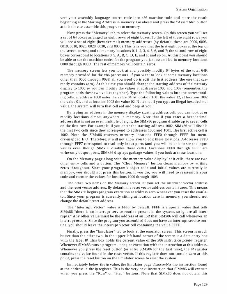
System Organization
Page 129
vert your assembly language source code into x86 machine code and store the resultbeginning at the Starting Address in memory. Go ahead and press the “Assemble” buttonat this time to assemble this program to memory.
Now press the “Memory” tab to select the memory screen. On this screen you will seea set of 64 boxes arranged as eight rows of eight boxes. To the left of these eight rows youwill see a set of eight (hexadecimal) memory addresses (by default, these are 0000, 0008,0010, 0018, 0020, 0028, 0030, and 0038). This tells you that the first eight boxes at the top ofthe screen correspond to memory locations 0, 1, 2, 3, 4, 5, 6, and 7; the second row of eightboxes correspond to locations 8, 9, A, B, C, D, E, and F; and so on. At this point you shouldbe able to see the machine codes for the program you just assembled in memory locations0000 through 000D. The rest of memory will contain zeros.
The memory screen lets you look at and possibly modify 64 bytes of the total 64Kmemory provided for the x86 processors. If you want to look at some memory locationsother than 0000 through 003F, all you need do is edit the first address (the one that cur-rently contains zero). At this time you should change the starting address of the memorydisplay to 1000 so you can modify the values at addresses 1000 and 1002 (remember, theprogram adds these two values together). Type the following values into the correspond-ing cells: at address 1000 enter the value 34, at location 1001 the value 12, at location 1002the value 01, and at location 1003 the value 02. Note that if you type an illegal hexadecimalvalue, the system will turn that cell red and beep at you.
By typing an address in the memory display starting address cell, you can look at ormodify locations almost anywhere in memory. Note that if you enter a hexadecimaladdress that is not an even multiple of eight, the SIMx86 program disable up to seven cellson the first row. For example, if you enter the starting address 1002, SIMx86 will disablethe first two cells since they correspond to addresses 1000 and 1001. The first active cell is1002. Note the SIMx86 reserves memory locations FFF0 through FFFF for mem-ory-mapped I/O. Therefore, it will not allow you to edit these locations. Addresses FFF0through FFF7 correspond to read-only input ports (and you will be able to see the inputvalues even though SIMx86 disables these cells). Locations FFF8 through FFFF arewrite-only output ports, SIMx86 displays garbage values if you look at these locations.
On the Memory page along with the memory value display/edit cells, there are twoother entry cells and a button. The “Clear Memory” button clears memory by writingzeros throughout. Since your program’s object code and initial values are currently inmemory, you should not press this button. If you do, you will need to reassemble yourcode and reenter the values for locations 1000 through 1003.
The other two items on the Memory screen let you set the interrupt vector addressand the reset vector address. By default, the reset vector address contains zero. This meansthat the SIMx86 begins program execution at address zero whenever you reset the emula-tor. Since your program is currently sitting at location zero in memory, you should notchange the default reset address.
The “Interrupt Vector” value is FFFF by default. FFFF is a special value that tellsSIMx86 “there is no interrupt service routine present in the system, so ignore all inter-rupts.” Any other value must be the address of an ISR that SIMx86 will call whenever aninterrupt occurs. Since the program you assembled does not have an interrupt service rou-tine, you should leave the interrupt vector cell containing the value FFFF.
Finally, press the “Emulator” tab to look at the emulator screen. This screen is muchbusier than the other two. In the upper left hand corner of the screen is a data entry boxwith the label IP. This box holds the current value of the x86 instruction pointer register.Whenever SIMx86 runs a program, it begins execution with the instruction at this address.Whenever you press the reset button (or enter SIMx86 for the first time), the IP registercontains the value found in the reset vector. If this register does not contain zero at thispoint, press the reset button on the Emulator screen to reset the system.
Immediately below the ip value, the Emulator page disassembles the instruction foundat the address in the ip register. This is the very next instruction that SIMx86 will executewhen you press the “Run” or “Step” buttons. Note that SIMx86 does not obtain this
Chapter 03
Page 130
instruction from the source code window on the Editor screen. Instead, it decodes theopcode in memory (at the address found in ip) and generates this string itself. Therefore,there may be minor differences between the instruction you wrote and the instructionSIMx86 displays on this page. Note that a disassembled instruction contains severalnumeric values in front of the actual instruction. The first (four-digit) value is the memoryaddress of that instruction. The next pair of digits (or the next three pairs of digits) are theopcodes and possible instruction operand values. For example, the mov ax, [1000] instruc-tion’s machine code is C6 00 10 since these are the three sets of digits appearing at thispoint.
Below the current disassembled instruction, SIMx86 displays 15 instructions it disas-sembles. The starting address for this disassemble is not the value in the ip register.Instead, the value in the lower right hand corner of the screen specifies the starting disas-sembly address. The two little arrows next to the disassembly starting address let youquickly increment or decrement the disassembly starting address. Assuming the startingaddress is zero (change it to zero if it is not), press the down arrow. Note that this incre-ments the starting address by one. Now look back at the disassembled listing. As you cansee, pressing the down arrow has produced an interesting result. The first instruction (ataddress 0001) is “****”. The four asterisks indicate that this particular opcode is an illegalinstruction opcode. The second instruction, at address 0002, is not ax. Since the programyou assembled did not contain an illegal opcode or a not ax instruction, you may be won-dering where these instructions came from. However, note the starting address of the firstinstruction: 0001. This is the second byte of the first instruction in your program. In fact,the illegal instruction (opcode=00) and the not ax instruction (opcode=10) are actually adisassembly of the mov ax, [1000] two-byte operand. This should clearly demonstrate aproblem with disassembly – it is possible to get “out of phase” by specify a startingaddress that is in the middle of a multi-byte instruction. You will need to consider thiswhen disassembling code.
In the middle of the Emulator screen there are several buttons: Run, Step, Halt, Inter-rupt, and Reset (the “Running” box is an annunciator, not a button). Pressing the Run but-ton will cause the SIMx86 program to run the program (starting at the address in the ipregister) at “full” speed. Pressing the Step button instructs SIMx86 to execute only theinstruction that ip points at and then stop. The Halt button, which is only active while aprogram is running, will stop execution. Pressing the Interrupt button generates an inter-rupt and pressing the Reset button resets the system (and halts execution if a program iscurrently running). Note that pressing the Reset button clears the x86 registers to zero andloads the ip register with the value in the reset vector.
The “Running” annunciator is gray if SIMx86 is not currently running a program. Itturns red when a program is actually running. You can use this annunciator as an easyway to tell if a program is running if the program is busy computing something (or is inan infinite loop) and there is no I/O to indicate program execution.
The boxes with the ax, bx, cx, and dx labels let you modify the values of these registerswhile a program is not running (the entry cells are not enabled while a program is actuallyrunning). These cells also display the current values of the registers whenever a programstops or between instructions when you are stepping through a program. Note that whilea program is running the values in these cells are static and do not reflect their current val-ues.
The “Less” and “Equal” check boxes denote the values of the less than and equalflags. The x86 cmp instruction sets these flags depending on the result of the comparison.You can view these values while the program is not running. You can also initialize themto true or false by clicking on the appropriate box with the mouse (while the program isnot running).
In the middle section of the Emulator screen there are four “LEDs” and four “toggleswitches.” Above each of these objects is a hexadecimal address denoting their mem-ory-mapped I/O addresses. Writing a zero to a corresponding LED address turns thatLED “off” (turns it white). Writing a one to a corresponding LED address turns that LED
System Organization
Page 131
“on” (turns it red). Note that the LEDs only respond to bit zero of their port addresses.These output devices ignore all other bits in the value written to these addresses.
The toggle switches provide four memory-mapped input devices. If you read theaddress above each switch SIMx86 will return a zero if the switch is off. SIMx86 willreturn a one if the switch is in the on position. You can toggle a switch by clicking on itwith the mouse. Note that a little rectangle on the switch turns red if the switch is in the“on” position.
The two columns on the right side of the Emulate screen (“Input” and “Output”) dis-play input values read with the get instruction and output values the put instructionprints.
For this first exercise, you will use the Step button to single step through each of theinstructions in the EX1.x86 program. First, begin by pressing the Reset button22. Next,press the Step button once. Note that the values in the ip and ax registers change. The ipregister value changes to 0003 since that is the address of the next instruction in memory,ax’s value changed to 1234 since that’s the value you placed at location 1000 when operat-ing on the Memory screen. Single step through the remaining instructions (by repeatedlypressing Step) until you get the “Halt Encountered” dialog box.
For your lab report: explain the results obtained after the execution of each instruc-tion. Note that single-stepping through a program as you’ve done here is an excellent wayto ensure that you fully understand how the program operates. As a general rule, youshould always single-step through every program you write when testing it.
3.6.2 Simple I/O-Mapped Input/Output Operations
Go to the Editor screen and load the EX2.x86 file into the editor. This program intro-duces some new concepts, so take a moment to study this code:
mov bx, 1000a: get
mov [bx], axadd bx, 2cmp ax, 0jne a
mov cx, bxmov bx, 1000mov ax, 0
b: add ax, [bx]add bx, 2cmp bx, cxjb b
puthalt
The first thing to note are the two strings “a:” and “b:” appearing in column one of thelisting. The SIMx86 assembler lets you specify up to 26 statement labels by specifying a sin-gle alphabetic character followed by a colon. Labels are generally the operand of a jumpinstruction of some sort. Therefore, the “jne a” instruction above really says “jump if notequal to the statement prefaced with the ‘a:’ label” rather than saying “jump if not equal tolocation ten (0Ah) in memory.”
Using labels is much more convenient than figuring out the address of a targetinstruction manually, especially if the target instruction appears later in the code. TheSIMx86 assembler computes the address of these labels and substitutes the correct address
22. It is a good idea to get in the habit of pressing the Reset button before running or stepping through any pro-gram.
Chapter 03
Page 132
for the operands of the jump instructions. Note that you can specify a numeric address inthe operand field of a jump instruction. However, all numeric addresses must begin witha decimal digit (even though they are hexadecimal values). If your target address wouldnormally begin with a value in the range A through F, simply prepend a zero to the num-ber. For example, if “jne a” was supposed to mean “jump if not equal to location 0Ah” youwould write the instruction as “jne 0a”.
This program contains two loops. In the first loop, the program reads a sequence ofvalues from the user until the user enters the value zero. This loop stores each word intosuccessive memory locations starting at address 1000h. Remember, each word read by theuser requires two bytes; this is why the loop adds two to bx on each iteration.
The second loop in this program scans through the input values and computes theirsum. At the end of the loop, the code prints the sum to the output window using the putinstruction.
For your lab report: single-step through this program and describe how each instruc-tion works. Reset the x86 and run this program at full speed. Enter several values anddescribe the result. Discuss the get and put instruction. Describe why they doI/O-mapped input/output operations rather than memory-mapped input/output opera-tions.
3.6.3 Memory Mapped I/O
From the Editor screen, load the EX3.x86 program file. That program takes the follow-ing form (the comments were added here to make the operation of this program clearer):
a: mov ax, [fff0]mov bx, [fff2]
mov cx, ax ;Computes Sw0 and Sw1and cx, bxmov [fff8], cx
mov cx, ax ;Computes Sw0 or Sw1or cx, bxmov [fffa], cx
mov cx, ax ;Computes Sw0 xor Sw1mov dx, bx ;Remember, xor = AB’ + A’Bnot cxnot bxand cx, bxand dx, axor cx, dxmov [fffc], cx
not cx ;Computes Sw0 = Sw1mov [fffe], cx ;Remember, equals = not xor
mov ax, [fff4] ;Read the third switch.cmp ax, 0 ;See if it’s on.je a ;Repeat this program while off.halt
Locations 0FFF0h, 0FFF2h, and 0FFF4h correspond to the first three toggle switcheson the Execution page. These are memory-mapped I/O devices that put a zero or one intothe corresponding memory locations depending upon whether the toggle switch is in theon or off state. Locations 0FFF8h, 0FFFAh, 0FFFCh, and 0FFFEh correspond to the fourLEDs. Writing a zero to these locations turns the corresponding LED off, writing a oneturns it on.
System Organization
Page 133
This program computes the logical and, or, xor, and xnor (not xor) functions for thevalues read from the first two toggle switches. This program displays the results of thesefunctions on the four output LEDs. This program reads the value of the third toggleswitch to determine when to quit. When the third toggle switch is in the on position, theprogram will stop.
For your lab report: run this program and cycle through the four possible combina-tions of on and off for the first two switches. Include the results in your lab report.
3.6.4 DMA Exercises
In this exercise you will start a program running (EX4.x86) that examines and oper-ates on values found in memory. Then you will switch to the Memory screen and modifyvalues in memory (that is, you will directly access memory while the program continuesto run), thus simulating a peripheral device that uses DMA.
The EX4.x86 program begins by setting memory location 1000h to zero. Then it loopsuntil one of two conditions is met – either the user toggles the FFF0 switch or the userchanges the value in memory location 1000h. Toggling the FFF0 switch terminates the pro-gram. Changing the value in memory location 1000h transfers control to a section of theprogram that adds together n words, where n is the new value in memory location 1000h.The program sums the words appearing in contiguous memory locations starting ataddress 1002h. The actual program looks like the following:
d: mov cx, 0 ;Clear location 1000h before wemov [1000], cx ; begin testing it.
; The following loop checks to see if memory location 1000h changes or if; the FFF0 switch is in the on position.
a: mov cx, [1000] ;Check to see if location 1000hcmp cx, 0 ; changes. Jump to the section thatjne c ; sums the values if it does.
mov ax, [fff0] ;If location 1000h still contains zero,cmp ax, 0 ; read the FFF0 switch and see if it isje a ; off. If so, loop back. If the switchhalt ; is on, quit the program.
; The following code sums up the “cx” contiguous words of memory starting at; memory location 1002. After it sums up these values, it prints their sum.
c: mov bx, 1002 ;Initialize BX to point at data array.mov ax, 0 ;Initialize the sum
b: add ax, [bx] ;Sum in the next array value.add bx, 2 ;Point BX at the next item in the array.sub cx, 1 ;Decrement the element count.cmp cx, 0 ;Test to see if we’ve added up all thejne b ; values in the array.
put ;Print the sum and start over.jmp d
Load this program into SIMx86 and assemble it. Switch to the Emulate screen, pressthe Reset button, make sure the FFF0 switch is in the off position, and then run the pro-gram. Once the program is running switch to the memory screen by pressing the Memorytab. Change the starting display address to 1000. Change the value at location 1000h to 5.Switch back to the emulator screen. Assuming memory locations 1002 through 100B allcontain zero, the program should display a zero in the output column.
Switch back to the memory page. What does location 1000h now contain? Change theL.O. bytes of the words at address 1002, 1004, and 1006 to 1, 2, and 3, respectively. Change
Chapter 03
Page 134
the value in location 1000h to three. Switch to the Emulator page. Describe the output inyour lab report. Try entering other values into memory. Toggle the FFF0 switch when youwant to quit running this program.
For your lab report: explain how this program uses DMA to provide program input.Run several tests with different values in location 1000h and different values in the dataarray starting at location 1002. Include the results in your report.
For additional credit: Store the value 12 into memory location 1000. Explain why theprogram prints two values instead of just one value.
3.6.5 Interrupt Driven I/O Exercises
In this exercise you will load two programs into memory: a main program and aninterrupt service routine. This exercise demonstrates the use of interrupts and an interruptservice routine.
The main program (EX5a.x86) will constantly compare memory locations 1000h and1002h. If they are not equal, the main program will print the value of location 1000h andthen copy this value to location 1002h and repeat this process. The main program repeatsthis loop until the user toggles switch FFF0 to the on position. The code for the main pro-gram is the following:
a: mov ax, [1000] ;Fetch the data at location 1000h andcmp ax, [1002] ; see if it is the same as location je b ; 1002h. If so, check the FFF0 switch.put ;If the two values are different, printmov [1002], ax ; 1000h’s value and make them the same.
b: mov ax, [fff0] ;Test the FFF0 switch to see if we cmp ax, 0 ; should quit this program.je ahalt
The interrupt service routine (EX5b.x86) sits at location 100h in memory. Whenever aninterrupt occurs, this ISR simply increments the value at location 1000h by loading thisvalue into ax, adding one to the value in ax, and then storing this value back to location1000h. After these instructions, the ISR returns to the main program. The interrupt serviceroutine contains the following code:
mov ax, [1000] ;Increment location 1000h by one andadd ax, 1 ; return to the interrupted code.mov [1000], axiret
You must load and assemble both files before attempting to run the main program.Begin by loading the main program (EX5a.x86) into memory and assemble it at addresszero. Then load the ISR (EX5b.x86) into memory, set the Starting Address to 100, and thenassemble your code. Warning: if you forget to change the starting address you will wipe outyour main program when you assemble the ISR. If this happens, you will need to repeat this proce-dure from the beginning.
After assembling the code, the next step is to set the interrupt vector so that it containsthe address of the ISR. To do this, switch to the Memory screen. The interrupt vector cellshould currently contain 0FFFFh (this value indicates that interrupts are disabled).Change this to 100 so that it contains the address of the interrupt service routine. This alsoenables the interrupt system.
Finally, switch to the Emulator screen, make sure the FFF0 toggle switch is in the offposition, reset the program, and start it running. Normally, nothing will happen. Nowpress the interrupt button and observe the results.
System Organization
Page 135
For your lab report: describe the output of the program whenever you press the inter-rupt button. Explain all the steps you would need to follow to place the interrupt serviceroutine at address 2000h rather than 100h.
For additional credit: write your own interrupt service routine that does somethingsimple. Run the main program and press the interrupt button to test your code. Verify thatyour ISR works properly.
3.6.6 Machine Language Programming & Instruction Encoding Exercises
To this point you have been creating machine language programs with SIMx86’sbuilt-in assembler. An assembler is a program that translates an ASCII source file contain-ing textual representations of a program into the actual machine code. The assembler pro-gram saves you a considerable amount of work by translating human readableinstructions into machine code. Although tedious, you can perform this translation your-self. In this exercise you will create some very short machine language programs by encod-ing the instructions and entering their hexadecimal opcodes into memory on the memoryscreen.
Using the instruction encodings found in Figure 3.19, Figure 3.20, Figure 3.21, andFigure 3.22, write the hexadecimal values for the opcodes beside each of the followinginstructions:
You can assume that the program starts at address zero and, therefore, label “a” will be ataddress 0003 since the mov cx, 0 instruction is three bytes long.
mov cx, 0
a: get
put
add ax, ax
put
add ax, ax
put
add ax, ax
put
add cx, 1
cmp cx, 4
jb a
halt
Binary Opcode Hex Operand

Chapter 03
Page 136
For your lab report: enter the hexadecimal opcodes and operands into memory start-ing at location zero using the Memory editor screen. Dump these values and include themin your lab report. Switch to the Emulator screen and disassemble the code starting ataddress zero. Verify that this code is the same as the assembly code above. Print a copy ofthe disassembled code and include it in your lab report. Run the program and verify thatit works properly.
3.6.7 Self Modifying Code Exercises
In the previous laboratory exercise, you discovered that the system doesn’t really dif-ferentiate data and instructions in memory. You were able to enter hexadecimal data andthe x86 processor treats it as a sequence of executable instructions. It is also possible for aprogram to store data into memory and then execute it. A program is self-modifying if itcreates or modifies some of the instructions it executes.
Consider the following x86 program (EX6.x86):
sub ax, axmov [100], ax
a: mov ax, [100]cmp ax, 0je bhalt
b: mov ax, 00c6mov [100], axmov ax, 0710mov [102], axmov ax, a6a0mov [104], axmov ax, 1000mov [106], axmov ax, 8007mov [108], axmov ax, 00e6mov [10a], axmov ax, 0e10mov [10c], axmov ax, 4mov [10e], axjmp 100
This program writes the following code to location 100 and then executes it:
mov ax, [1000]putadd ax, axadd ax, [1000]putsub ax, axmov [1000], axjmp 0004 ;0004 is the address of the A: label.
For your lab report: execute the EX7.x86 program and verify that it generates theabove code at location 100.
Although this program demonstrates the principle of self-modifying code, it hardlydoes anything useful. As a general rule, one would not use self-modifying code in themanner above, where one segment writes some sequence of instructions and then exe-cutes them. Instead, most programs that use self-modifying code only modify existinginstructions and often only the operands of those instructions.
System Organization
Page 137
Self-modifying code is rarely found in modern assembly language programs. Pro-grams that are self-modifying are hard to read and understand, difficult to debug, andoften unstable. Programmers often resort to self-modifying code when the CPU’s architec-ture lacks sufficient power to achieve a desired goal. The later Intel 80x86 processors donot lack for instructions or addressing modes, so it is very rare to find 80x86 programs thatuse self-modifying code23. The x86 processors, however, have a very weak instruction set,so there are actually a couple of instances where self-modifying code may prove useful.
A good example of an architectural deficiency where the x86 is lacking is with respectto subroutines. The x86 instruction set does not provide any (direct) way to call and returnfrom a subroutine. However, you can easily simulate a call and return using the jmpinstruction and self-modifying code. Consider the following x86 “subroutine” that sits atlocation 100h in memory:
; Integer to Binary converter.; Expects an unsigned integer value in AX.; Converts this to a string of zeros and ones storing this string of; values into memory starting at location 1000h.
mov bx, 1000 ;Starting address of string.mov cx, 10 ;16 (10h) digits in a word.
a: mov dx, 0 ;Assume current bit is zero.cmp ax, 8000 ;See if AX’s H.O. bit is zero or one.jb b ;Branch if AX’x H.O. bit is zero.mov dx, 1 ;AX’s H.O. bit is one, set that here.
b: mov [bx], dx ;Store zero or one to next string loc.add bx, 1 ;Bump BX up to next string location.add ax, ax ;AX = AX *2 (shift left operation).sub cx, 1 ;Count off 16 bits.cmp cx, 0 ;Repeat 16 times.ja ajmp 0 ;Return to caller via self-mod code.
The only instruction that a program will modify in this subroutine is the very last jmpinstruction. This jump instruction must transfer control to the first instruction beyond thejmp in the calling code that transfers control to this subroutine; that is, the caller must storethe return address into the operand of the jmp instruction in the code above. As it turnsout, the jmp instruction is at address 120h (assuming the code above starts at location100h). Therefore, the caller must store the return address into location 121h (the operandof the jmp instruction). The following sample “main” program makes three calls to the“subroutine” above:
mov ax, 000c ;Address of the BRK instr below.mov [121], ax ;Store into JMP as return address.mov ax, 1234 ;Convert 1234h to binary.jmp 100 ;”Call” the subroutine above.brk ;Pause to let the user examine 1000h.
mov ax, 0019 ;Address of the brk instr below.mov [121], axmov ax, fdeb ;Convert 0FDEBh to binary.jmp 100brk
mov ax, 26 ;Address of the halt instr below.mov [121], axmov ax, 2345 ;Convert 2345h to binary.jmp 100
halt
23. Many viruses and copy protection programs use self modifying code to make it difficult to detect or bypassthem.
Chapter 03
Page 138
Load the subroutine (EX7s.x86) into SIMx86 and assemble it starting at location 100h.Next, load the main program (EX7m.x86) into memory and assemble it starting at locationzero. Switch to the Emulator screen and verify that all the return addresses (0ch, 19h, and26h) are correct. Also verify that the return address needs to be written to location 121h.Next, run the program. The program will execute a brk instruction after each of the firsttwo calls. The brk instruction pauses the program. At this point you can switch to thememory screen at look at locations 1000-100F in memory. They should contain thepseudo-binary conversion of the value passed to the subroutine. Once you verify that theconversion is correct, switch back to the Emulator screen and press the Run button to con-tinue program execution after the brk.
For your lab report: describe how self-modifying code works and explain in detailhow this code uses self-modifying code to simulate call and return instructions. Explainthe modifications you would need to make to move the main program to address 800hand the subroutine to location 900h.
For additional credit: Actually change the program and subroutine so that they workproperly at the addresses above (800h and 900h).
3.7 Programming Projects
Note: You are to write these programs in x86 assembly language code using theSIMx86 program. Include a specification document, a test plan, a program listing, andsample output with your program submissions
1) The x86 instruction set does not include a multiply instruction. Write a short program thatreads two values from the user and displays their product (hint: remember that multipli-cation is just repeated addition).
2) Create a callable subroutine that performs the multplication inproblem (1) above. Pass thetwo values to multiple to the subroutine in the ax and bx registers. Return the product inthe cx register. Use the self-modifying code technique found in the section “Self ModifyingCode Exercises” on page 136.
3) Write a program that reads two two-bit numbers from switches (FFF0/FFF2) and(FFF4/FFF6). Treating these bits as logical values, your code should compute the three-bitsum of these two values (two-bit result plus a carry). Use the logic equations for the fulladder from the previous chapter. Do not simply add these values using the x86 add instruction.Display the three-bit result on LEDs FFF8, FFFA, and FFFC.
4) Write a subroutine that expects an address in BX, a count in CX, and a value in AX. Itshould write CX copies of AX to successive words in memory starting at address BX.Write a main program that calls this subroutine several times with different addresses.Use the self-modifying code subroutine call and return mechanism described in the labo-ratory exercises.
5) Write the generic logic function for the x86 processor (see Chapter Two). Hint: add ax, axdoes a shift left on the value in ax. You can test to see if the high order bit is set by checkingto see if ax is greater than 8000h.
6) Write a program that reads the generic function number for a four-input function from theuser and then continually reads the switches and writes the result to an LED.
7) Write a program that scans an array of words starting at address 1000h and memory, ofthe length specified by the value in cx, and locates the maximum value in that array. Dis-play the value after scanning the array.
8) Write a program that computes the two’s complement of an array of values starting atlocation 1000h. CX should contain the number of values in the array. Assume each arrayelement is a two-byte integer.
9) Write a “light show” program that displays a “light show” on the SIMx86’s LEDs. Itshould accomplish this by writing a set of values to the LEDs, delaying for some time

System Organization
Page 139
period (by executing an empty loop) and then repeating the process over and over again.Store the values to write to the LEDs in an array in memory and fetch a new set of LEDvalues from this array on each loop iteration.
10) Write a simple program that sorts the words in memory locations 1000..10FF in ascendingorder. You can use a simple insertion sort algorithm. The Pascal code for such a sort is
for i := 0 to n-1 dofor j := i+1 to n do
if (memory[i] > memory[j]) then begin
temp := memory[i];memory[i] := memory[j];memory[j] := temp;
end;
3.8 Summary
Writing good assembly language programs requires a strong knowledge of the under-lying hardware. Simply knowing the instruction set is insufficient. To produce the bestprograms, you must understand how the hardware executes your programs and accessesdata.
Most modern computer systems store programs and data in the same memory space(the Von Neumann architecture). Like most Von Neumann machines, a typical 80x86 systemhas three major components: the central processing unit (CPU), input/output (I/O), andmemory. See:
• “The Basic System Components” on page 83
Data travels between the CPU, I/O devices, and memory on the system bus. There arethree major busses employed by the 80x86 family, the address bus, the data bus, and the con-trol bus. The address bus carries a binary number which specifies which memory locationor I/O port the CPU wishes to access; the data bus carries data between the CPU andmemory or I/O; the control bus carries important signals which determine whether theCPU is reading or writing memory data or accessing an I/O port. See:
• “The System Bus” on page 84• “The Data Bus” on page 84• “The Address Bus” on page 86• “The Control Bus” on page 86
The number of data lines on the data bus determines the size of a processor. When wesay that a processor is an eight bit processor we mean that it has eight data lines on its databus. The size of the data which the processor can handle internally on the CPU does notaffect the size of that CPU. See:
• “The Data Bus” on page 84• “The “Size” of a Processor” on page 85
The address bus transmits a binary number from the CPU to memory and I/O toselect a particular memory element or I/O port. The number of lines on the address bussets the maximum number of memory locations the CPU can access. Typical address bussizes on the 80x86 CPUs are 20, 24, and 32 bits. See:
• “The Address Bus” on page 86
The 80x86 CPUs also have a control bus which contains various signals necessary forthe proper operation of the system. The system clock, read/write control signals, and I/Oor memory control signals are some samples of the many lines which appear on the con-trol bus. See:
• “The Control Bus” on page 86
Chapter 03
Page 140
The memory subsystem is where the CPU stores program instructions and data. On80x86 based systems, memory appears as a linear array of bytes, each with its own uniqueaddress. The address of the first byte in memory is zero, and the address of the last avail-able byte in memory is 2n-1, where n is the number of lines on the address bus. The 80x86stores words in two consecutive memory locations. The L.O. byte of the word is at thelowest address of those two bytes; the H.O. byte immediately follows the first at the nexthighest address. Although a word consumes two memory addresses, when dealing withwords we simply use the address of its L.O. byte as the address of that word. Doublewords consume four consecutive bytes in memory. The L.O. byte appears at the lowestaddress of the four, the H.O. byte appears at the highest address. The “address” of thedouble word is the address of its L.O. byte. See:
• “The Memory Subsystem” on page 87
CPUs with 16, 32, or 64 bit data busses generally organize memory in banks. A 16 bitmemory subsystem uses two banks of eight bits each, a 32 bit memory subsystem usesfour banks of eight bits each, and a 64 bit system uses eight banks of eight bits each.Accessing a word or double word at the same address within all the banks is faster thanaccessing an object which is split across two addresses in the different banks. Therefore,you should attempt to align word data so that it begins on an even address and doubleword data so that it begins on an address which is evenly divisible by four. You may placebyte data at any address. See:
• “The Memory Subsystem” on page 87
The 80x86 CPUs provide a separate 16 bit I/O address space which lets the CPUaccess any one of 65,536 different I/O ports. A typical I/O device connected to the IBM PConly uses 10 of these address lines, limiting the system to 1,024 different I/O ports. Themajor benefit to using an I/O address space rather than mapping all I/O devices to mem-ory space is that the I/O devices need not infringe upon the addressable memory space.To differentiate I/O and memory accesses, there are special control lines on the systembus. See:
• “The Control Bus” on page 86• “The I/O Subsystem” on page 92
The system clock controls the speed at which the processor performs basic operations.Most CPU activities occur on the rising or falling edge of this clock. Examples includeinstruction execution, memory access, and checking for wait states. The faster the systemclock runs, the faster your program will execute; however, your memory must be as fast asthe system clock or you will need to introduce wait states, which slow the system backdown. See:
• “System Timing” on page 92• “The System Clock” on page 92• “Memory Access and the System Clock” on page 93• “Wait States” on page 95
Most programs exhibit a locality of reference. They either access the same memory loca-tion repeatedly within a small period of time (temporal locality) or they access neighboringmemory locations during a short time period (spatial locality). A cache memory subsystemexploits this phenomenon to reduce wait states in a system. A small cache memory systemcan achieve an 80-95% hit ratio. Two-level caching systems use two different caches (typi-cally one on the CPU chip and one off chip) to achieve even better system performance.See:
• “Cache Memory” on page 96
CPUs, such as those in the 80x86 family, break the execution of a machine instructiondown into several distinct steps, each requiring one clock cycle. These steps include fetch-ing an instruction opcode, decoding that opcode, fetching operands for the instruction,computing memory addresses, accessing memory, performing the basic operation, andstoring the result away. On a very simplistic CPU, a simple instruction may take severalclock cycles. The best way to improve the performance of a CPU is to execute several
System Organization
Page 141
internal operations in parallel with one another. A simple scheme is to put an instructionprefetch queue on the CPU. This allows you to overlap opcode fetching and decodingwith instruction execution, often cutting the execution time in half. Another alternative isto use an instruction pipeline so you can execute several instructions in parallel. Finally,you can design a superscalar CPU which executes two or more instructions concurrently.These techniques will all improve the running time of your programs. See:
• “The 886 Processor” on page 110• “The 8286 Processor” on page 110• “The 8486 Processor” on page 116• “The 8686 Processor” on page 123
Although pipelined and superscalar CPUs improve overall system performance,extracting the best performance from such complex CPUs requires careful planning by theprogrammer. Pipeline stalls and hazards can cause a major loss of performance in poorlyorganized programs. By carefully organizing the sequence of the instructions in your pro-grams you can make your programs run as much as two to three times faster. See:
• “The 8486 Pipeline” on page 117• “Stalls in a Pipeline” on page 118• “Cache, the Prefetch Queue, and the 8486” on page 119• “Hazards on the 8486” on page 122• “The 8686 Processor” on page 123
The I/O subsystem is the third major component of a Von Neumann machine (mem-ory and the CPU being the other two). There are three primary ways to move databetween the computer system and the outside world: I/O-mapped input/output, mem-ory-mapped input/output, and direct memory access (DMA). For more information, see:
• “I/O (Input/Output)” on page 124
To improve system performance, most modern computer systems use interrupts toalert the CPU when an I/O operation is complete. This allows the CPU to continue withother processing rather than waiting for an I/O operation to complete (polling the I/Oport). For more information on interrupts and polled I/O operatoins, see:
• “Interrupts and Polled I/O” on page 126

Chapter 03
Page 142
3.9 Questions
1. What three components make up Von Neumann Machines?
2. What is the purpose of
a) The system busb) The address busc) The data busd) The control bus
3. Which bus defines the “size” of the processor?
4. Which bus controls how much memory you can have?
5. Does the size of the data bus control the maximum value the CPU can process? Explain.
6. What are the data bus sizes of:
a) 8088 b) 8086 c) 80286 d) 80386sxe) 80386 f) 80486 g) 80586/Pentium
7. What are the address bus sizes of the above processors?
8. How many “banks” of memory do each of the above processors have?
9. Explain how to store a word in byte addressable memory (that is, at what addresses).Explain how to store a double word.
10. How many memory operations will it take to read a word from the following addresseson the following processors?
11. Repeat the above for double words
12. Explain which addresses are best for byte, word, and doubleword variables on an 8088,80286, and 80386 processor.
13. How many different I/O locations can you address on the 80x86 chip? How many are typ-ically available on a PC?
14. What is the purpose of the system clock?
Table 21: Memory Cycles for Word Accesses
100 101 102 103 104 105
8088
80286
80386
Table 22: Memory Cycles for Doubleword Accesses
100 101 102 103 104 105
8088
80286
80386
System Organization
Page 143
15. What is a clock cycle?
16. What is the relationship between clock frequency and the clock period?
17. How many clock cycles are required for each of the following to read a byte from mem-ory?
a) 8088 b) 8086 c) 80486
18. What does the term “memory access time” mean?
19. What is a wait state?
20. If you are running an 80486 at the following clock speeds, how many wait states arerequired if you are using 80ns RAM (assuming no other delays)?
a) 20 MHz b) 25 MHz c) 33 MHz d) 50 MHz e) 100 MHz
21. If your CPU runs at 50 MHz, 20ns RAM probably won’t be fast enough to operate at zerowait states. Explain why.
22. Since sub-10ns RAM is available, why aren’t all system zero wait state systems?
23. Explain how the cache operates to save some wait states.
24. What is the difference between spatial and temporal locality of reference?
25. Explain where temporal and spatial locality of reference occur in the following Pascalcode:
while i < 10 do beginx := x * i;i := i + 1;
end;
26. How does cache memory improve the performance of a section of code exhibiting spatiallocality of reference?
27. Under what circumstances is a cache not going to save you any wait states?
28. What is the effective (average) number of wait states the following systems will operateunder?
a) 80% cache hit ratio, 10 wait states (WS) for memory, 0 WS for cache.b) 90% cache hit ratio; 7 WS for memory; 0 WS for cache.c) 95% cache hit ratio; 10 WS memory; 1 WS cache.d) 50% cache hit ratio; 2 WS memory; 0 WS cache.
29. What is the purpose of a two level caching system? What does it save?
30. What is the effective number of wait states for the following systems?
a) 80% primary cache hit ratio (HR) zero WS; 95% secondary cache HR with 2 WS; 10 WSfor main memory access.b) 50% primary cache HR, zero WS; 98% secondary cache HR, one WS; five WS for mainmemory access.c) 95% primary cache HR, one WS; 98% secondary cache HR, 4 WS; 10 WS for main mem-ory access.
31. Explain the purpose of the bus interface unit, the execution unit, and the control unit.
32. Why does it take more than one clock cycle to execute an instruction. Give some x86examples.
33. How does a prefetch queue save you time? Give some examples.
Chapter 03
Page 144
34. How does a pipeline allow you to (seemingly) execute one instruction per clock cycle?Give an example.
35. What is a hazard?
36. What happens on the 8486 when a hazard occurs?
37. How can you eliminate the effects of a hazard?
38. How does a jump (JMP/Jcc) instruction affect
a) The prefetch queue.b) The pipeline.
39. What is a pipeline stall?
40. Besides the obvious benefit of reducing wait states, how can a cache improve the perfor-mance of a pipelined system?
41. What is a Harvard Architecture Machine?
42. What does a superscalar CPU do to speed up execution?
43. What are the two main techniques you should use on a superscalar CPU to ensure yourcode runs as quickly as possible? (note: these are mechanical details, “Better Algorithms”doesn’t count here).
44. What is an interrupt? How does it improved system performance?
45. What is polled I/O?
46. What is the difference between memory-mapped and I/O mapped I/O?
47. DMA is a special case of memory-mapped I/O. Explain.