SYNTHESIS AND CHARACTERIZATION OF SCHOTTKY DIODES ON N …
66
University of Kentucky University of Kentucky UKnowledge UKnowledge University of Kentucky Master's Theses Graduate School 2008 SYNTHESIS AND CHARACTERIZATION OF SCHOTTKY DIODES SYNTHESIS AND CHARACTERIZATION OF SCHOTTKY DIODES ON N-TYPE CdTe NANOWIRES EMBEDDED IN POROUS ALUMINA ON N-TYPE CdTe NANOWIRES EMBEDDED IN POROUS ALUMINA TEMPLATES TEMPLATES Srikanth Yanamanagandla University of Kentucky Right click to open a feedback form in a new tab to let us know how this document benefits you. Right click to open a feedback form in a new tab to let us know how this document benefits you. Recommended Citation Recommended Citation Yanamanagandla, Srikanth, "SYNTHESIS AND CHARACTERIZATION OF SCHOTTKY DIODES ON N-TYPE CdTe NANOWIRES EMBEDDED IN POROUS ALUMINA TEMPLATES" (2008). University of Kentucky Master's Theses. 573. https://uknowledge.uky.edu/gradschool_theses/573 This Thesis is brought to you for free and open access by the Graduate School at UKnowledge. It has been accepted for inclusion in University of Kentucky Master's Theses by an authorized administrator of UKnowledge. For more information, please contact [email protected].
Transcript of SYNTHESIS AND CHARACTERIZATION OF SCHOTTKY DIODES ON N …

University of Kentucky University of Kentucky
UKnowledge UKnowledge
University of Kentucky Master's Theses Graduate School
2008
SYNTHESIS AND CHARACTERIZATION OF SCHOTTKY DIODES SYNTHESIS AND CHARACTERIZATION OF SCHOTTKY DIODES
ON N-TYPE CdTe NANOWIRES EMBEDDED IN POROUS ALUMINA ON N-TYPE CdTe NANOWIRES EMBEDDED IN POROUS ALUMINA
TEMPLATES TEMPLATES
Srikanth Yanamanagandla University of Kentucky
Right click to open a feedback form in a new tab to let us know how this document benefits you. Right click to open a feedback form in a new tab to let us know how this document benefits you.
Recommended Citation Recommended Citation Yanamanagandla, Srikanth, "SYNTHESIS AND CHARACTERIZATION OF SCHOTTKY DIODES ON N-TYPE CdTe NANOWIRES EMBEDDED IN POROUS ALUMINA TEMPLATES" (2008). University of Kentucky Master's Theses. 573. https://uknowledge.uky.edu/gradschool_theses/573
This Thesis is brought to you for free and open access by the Graduate School at UKnowledge. It has been accepted for inclusion in University of Kentucky Master's Theses by an authorized administrator of UKnowledge. For more information, please contact [email protected].

ABSTRACT OF THESIS
SYNTHESIS AND CHARACTERIZATION OF SCHOTTKY DIODES ON N-TYPE
CdTe NANOWIRES EMBEDDED IN POROUS ALUMINA TEMPLATES
This work focuses on the growth of vertically aligned CdTe nanowire arrays of
controllable diameter and length using cathodic electro deposition in anodized alumina
templates. This step was followed by annealing at 250° C in a reducing environment
(95% Ar + 5% H2). AAO template over ITO-glass was used as starting template for the
device fabrication. The deposited nanowires showed nanocrystalline cubic phase
structures with a strong preference in [111] direction. First gold (Au) was deposited into
AAO using cathodic electro deposition. This was followed by CdTe deposition into the
pore. Gold was deposited first as it aids the growth of CdTe inside AAO and it makes
Schottky contact with the deposited n type CdTe. CdTe was determined to be n-type from
the fact that back to back diode was obtained with Au-CdTe-Au test structure. Aluminum
(Al) was sputtered on the top to make the ohmic contact to the n type CdTe deposited in
AAO. Analysis of Schottky diodes yielded a diode ideality factor of 10.03 under dark and
10.08 under light and reverse saturation current density of 34.9µA/cm2 under dark and
39.7µA/cm2 under light.
KEYWORDS: Schottky diode, Cadmium Telluride (CdTe), Gold (Au), Nanowires,
Anodic Aluminum Oxide (AAO).
Srikanth Yanamanagandla
December 2nd
2008

SYNTHESIS AND CHARACTERIZATION OF SCHOTTKY DIODES ON N-TYPE
CADMIUM TELLURIDE (CdTe) NANOWIRES EMBEDDED IN POROUS
ALUMINA TEMPLATES
By
Srikanth Yanamanagandla
____________________________________
(Director of Thesis)
____________________________________
(Director of Graduate Studies)
____________________________________
(Date)

RULES FOR THE USE OF THESIS
Unpublished thesis submitted for the Master’s degree and deposited in the University of
Kentucky Library are as a rule open for inspection, but are to be used only with due
regard to the rights of the authors. Bibliographical references may be noted, but
quotations or summaries of parts may be published only with the permission of the
author, and with the usual scholarly acknowledgments.
Extensive copying or publication of the dissertation in whole or in part also requires the
consent of the Dean of the Graduate School of the University of Kentucky.
A library that borrows this dissertation for use by its patrons is expected to secure the
signature of each user.
Name Date
________________________________________________________________________
________________________________________________________________________
________________________________________________________________________
________________________________________________________________________
________________________________________________________________________
________________________________________________________________________
________________________________________________________________________
________________________________________________________________________
________________________________________________________________________

THESIS
Srikanth Yanamanagandla
The Graduate School
University of Kentucky
2008

SYNTHESIS AND CHARACTERISTIZATION OF SCHOTTKY DIODES ON N-
TYPE CADMIUM TELLURIDE (CdTe) NANOWIRES EMBEDDED IN POROUS
ALUMINA TEMPLATES
THESIS
A thesis submitted in partial fulfillment of the requirements for the degree of Master
of Science in the College of Engineering at the
University of Kentucky
By
Srikanth Yanamanagandla
Lexington, Kentucky
Director: Dr. Vijay P. Singh, Professor
Electrical and Computer Engineering
Lexington, Kentucky
2008

DEDICATED
To my first Teachers: Mom, Dad and Sister

iii
ACKOWLEDGEMETS
I would like to take this opportunity to express my sincere and heartfelt gratitude
to my academic advisor and thesis chair Dr. Vijay P. Singh for his guidance and support
throughout my thesis. I also would like to extend my thanks to Dr. Robert J. Heath and
Dr. Janet K. Lumpp for serving on my thesis committee and providing me with
invaluable comments and suggestions for improving this thesis.
I extend my heartfelt thanks to Dr. Suresh Rajaputra without whom the thesis
would have never taken its present shape. I am greatly indebted for his technical and
emotional support throughout my thesis. I am very thankful to Dr. Leonidas Bachas for
allowing me to work in his lab. I would also like to thank Mr. Henry Francis and
Mr. Jason Bachus for helping me out with XRD measurements. Many thanks go to
Mr. Karthik Venkatachalam for his valuable advice in chemical kinetics, supervision in
electrodeposition. I would also like to thank other members of the group in particular
Dr. Sovannary Phok, Mr. Sai Manohar Reddy Guduru, Mr. Piao Liu, Mr. Gautam
Chintakula and Mr. Sandeep Marda for their technical suggestions and intellectual
discussions. I would also like to thank Mr. Lucas G Taylor for helping me out with
diagrams. I would also like to thank my room-mates who are the family away from home
for their constant support and uplifting my spirits during difficult times.
Lastly and most importantly, I wish to thank my parents and my sister. They bore
me, raised me, supported me, taught me and loved me. They are my first teachers and I
dedicate this thesis to them.
iv
Table of Contents
ACKOWLEDGEMETS ............................................................................................ iii
List of Figures ................................................................................................................... vi
List of Tables .................................................................................................................... ix
1 Introduction ............................................................................................................... 1
1.1 Need for Solar Cells ............................................................................................. 1
1.2 Thin Film p-n junction based Solar Cells............................................................. 2
1.2.1 CdTe based Solar Cells ................................................................................. 2
1.2.2 Nanostructure based Solar Cells ................................................................... 3
1.3 Nano structure based CdTe homojunction Solar Cell .......................................... 4
2 Theory ........................................................................................................................ 6
2.1 Metal Semiconductor Junction ............................................................................. 6
2.1.1 Schottky Contact ........................................................................................... 7
2.1.2 Ohmic Contacts ........................................................................................... 10
2.2 Schottky Diode Characteristics .......................................................................... 12
2.3 Device Structure ................................................................................................. 14
3 Experimental Procedure ........................................................................................ 16
3.1 Fabrication Procedure ........................................................................................ 16
3.1.1 Fabrication of Nanoporous Alumina using ITO-glass substrates ............... 16
3.1.2 Anodization ................................................................................................. 16
3.1.3 Electrodeposition of Au into AAO Template ............................................. 19
3.1.4 Electrodeposition of CdTe in AAO Template ............................................ 21
3.1.5 E-Beam Evaporation of Au and Al for contacts ......................................... 22
3.2 Characterization Procedure ................................................................................ 23

v
3.2.1 X-ray Diffraction ........................................................................................ 23
3.2.2 Ultraviolet-Visual Absorption Spectroscopy .............................................. 24
3.2.3 Field Emission Scanning Electron Microscopy .......................................... 24
3.2.4 J-V characterization and analysis ................................................................ 25
4 Results and Discussion ............................................................................................ 26
4.1 Electro deposition of CdTe inside AAO template over ITO-glass .................... 26
4.2 Characterization of CdTe nanowires using Scanning Electron Microscopy
(SEM) ............................................................................................................................ 28
4.3 X-Ray Diffraction Characteristics ...................................................................... 32
4.4 Optical Absorption ............................................................................................. 36
4.5 JV Characteristics ............................................................................................... 38
4.5.1 JV Characteristics of Au-CdTe Schottky junction inside AAO with Au on
top as contact............................................................................................................. 38
4.5.2 Comparison of Au and Al as contact .......................................................... 39
4.5.3 J-V characteristics of Au-Nanocrystalline CdTe ........................................ 40
4.5.4 J-V Characteristics of 100nm Au-CdTe-Al ................................................ 42
4.5.5 Calculation of Resistivity (ρ) of deposited CdTe nanowires ...................... 44
4.6 Calculating Intrinsic barrier potential Vbi .......................................................... 46
4.7 Device Operation................................................................................................ 47
5 Conclusions and Future work ................................................................................ 48
References:....................................................................................................................... 49
Vita ................................................................................................................................... 52

vi
List of Figures
Figure 1-1: Device structure of proposed nanostructure based CdTe homojunction solar
cell with illumination from the top ..................................................................................... 5
Figure 2-1: Schottky barrier between a metal and an n-type semiconductor with Φm >
Φs; (a) band diagrams before contact; (b) equivalent band diagram after the contact ....... 8
Figure 2-2: Schottky barrier between a metal and a p-type semiconductor with Φm < Φs;
(a) band diagrams before contact; (b) equivalent band diagram after the contact .............. 9
Figure 2-3: Ohmic contact between a metal and an n-type semiconductor with Φm <
Φs; (a) band diagrams before contact; (b) equivalent band diagram after the contact ...... 10
Figure 2-4: Ohmic contact between a metal and a p-type semiconductor with Φm >
Φs; (a) band diagrams before contact; (b) equivalent band diagram after the contact ...... 11
Figure 2-5: Bias characteristics of a metal- n type semiconductor Schottky junction; (a)
Forward bias, (b) Reverse bias .......................................................................................... 13
Figure 2-6: 2 Dimensional view of the cross section of CdTe nanowires based Schottky
diode with Al on top as contact (ohmic) and Au as Schottky contact to CdTe wire at the
bottom ............................................................................................................................... 14
Figure 2-7: 3 dimensional view of Au-CdTe Schottky diode with Al on top as ohmic
contact ............................................................................................................................... 15
Figure 2-8: 3 dimensional view of Au-CdTe Schottky diode with Au on top as Schottky
contact ............................................................................................................................... 15
Figure 3-1: Current-time and Voltage-time plots during 1st step anodization ................. 17
Figure 3-2: Current-time and Voltage-time plots during 2nd step anodization ................ 19
Figure 3-3: Electrodeposition setup for 2 electrode process ............................................. 20
Figure 3-4: Electrodeposition setup for 3 Electrode process ............................................ 21
Figure 4-1: Current-Time plot against working electrode with respect to counter electrode
during Electro-deposition of CdTe ................................................................................... 26

vii
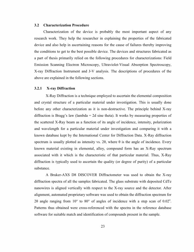
Figure 4-2: Cross section of a typical AAO template over ITO glass .............................. 28
Figure 4-3: SEM micrographs (a) top view and (b) top view showing a bundle of
nanowires on top ............................................................................................................... 29
Figure 4-4: Cross section of CdTe nanowires deposited on AAO/ITO ............................ 30
Figure 4-5: SEM micrographs of nanocrystalline CdTe: (a) top view and (b) a closer view
on the top........................................................................................................................... 31
Figure 4-6: X-ray Diffraction pattern of electrodeposited synthetic tellurium from the
acidic bath at pH=1.6 ........................................................................................................ 32
Figure 4-7: X-ray diffraction pattern of electrodeposited CdTe from modified acidic bath
at pH=2.4 .......................................................................................................................... 33
Figure 4-8: X-ray Diffraction pattern of electrodeposited CdTe nanowires in AAO
template on a glass-ITO substrate ..................................................................................... 34
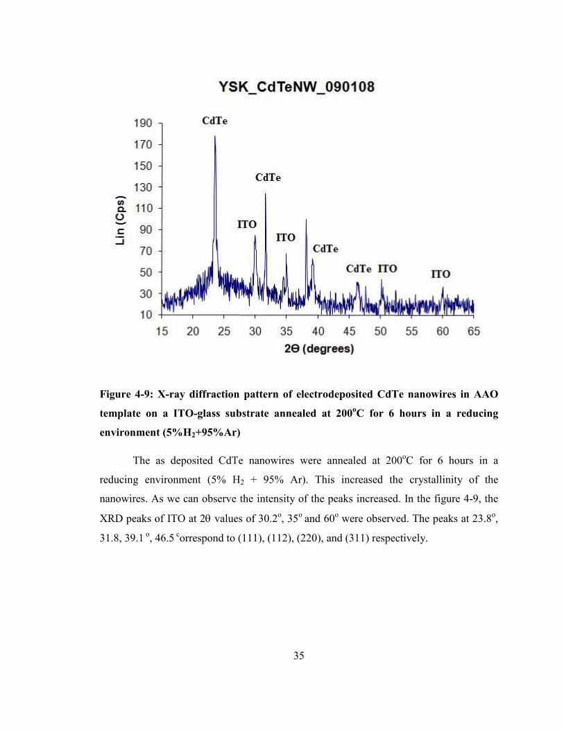
Figure 4-9: X-ray diffraction pattern of electrodeposited CdTe nanowires in AAO
template on a ITO-glass substrate annealed at 200oC for 6 hours in a reducing
environment (5%H2+95%Ar) ........................................................................................... 35
Figure 4-10: Optical absorption spectra of electrodeposited CdTe nanowires embedded in
an AAO template on a glass-ITO substrate ...................................................................... 36
Figure 4-11: Optical absorption spectra of electrodeposited nano crystalline CdTe ........ 37
Figure 4-12: JV characteristics of Au-CdTe-Au with Au-CdTe junction inside AAO
template ............................................................................................................................. 38
Figure 4-13: JV characteristics of Au-CdTe-Au and Au-CdTe-Al with Au-CdTe junction
inside AAO template......................................................................................................... 39
Figure 4-14: J-V characteristics of Au- nanocrystalline CdTe Schottky diode over ITO-
glass................................................................................................................................... 40
Figure 4-15: Plot of Ln(J) vs V of Au-nano crystalline CdTe-Al schottky diode ........... 41
Figure 4-16: J-V characteristics of Au-CdTe Schottky diode inside 100 nm long AAO
template over ITO-glass .................................................................................................... 42
Figure4-17: Plot of Ln(J) vs V of 100nm Au-CdTe-Al Schottky diode under dark ......... 43

viii
Figure 4-18: Plot of Ln(J) vs V of 100nm Au-CdTe-Al schottky diode under illumination
........................................................................................................................................... 43
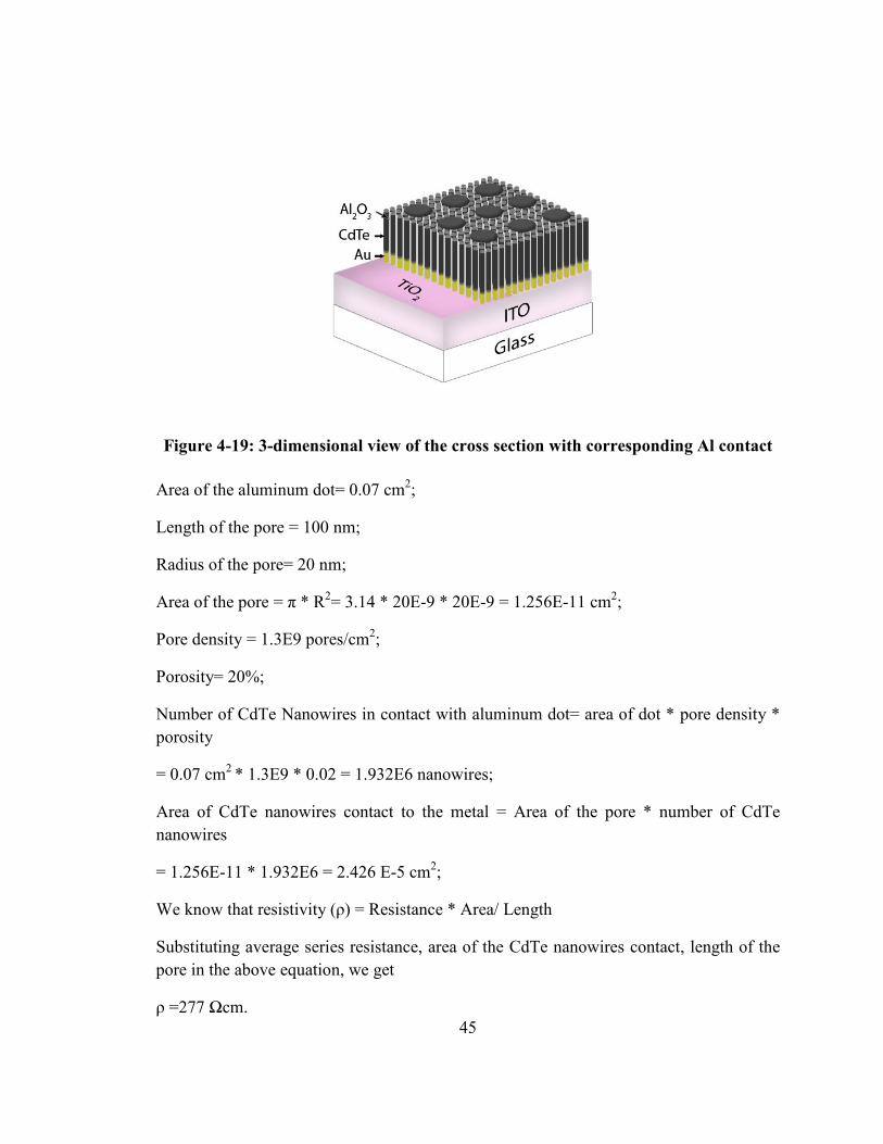
Figure 4-19: 3-dimensional view of the cross section with corresponding Al contact ..... 45
Figure 4-20: Band diagram of Au-CdTe junction embedded inside AAO; (a) band
diagrams before contact; (b) equivalent band diagram after the contact .......................... 47

ix
List of Tables
Table1: Phase formation of CdTe with varying concentrations of acidic bath ................. 36
Table 2: Diode parameters for Au-nanocrystalline CdTe Schottky diode ........................ 41
Table 3: Diode parameters for 100nm Au-CdTe-Al Schottky diode ................................ 44

1
1 Introduction
Energy and its spiraling cost is one of the major challenges facing humanity today.
Developing countries are consuming greater amounts of energy and conventional fuel
reserves (oil, gas, coal, etc.) are being depleted throughout the world. Energy demand in
the developing countries of Asia, which includes China and India, is expected to increase
by more than 100% by 20251. The rising cost of energy is leading to an increase in prices
of even basic commodities like food and water. If there is an effectively limitless supply
of energy, then costs can be controlled leading to a better economy and livelihood. This
cannot be achieved using fossil fuels and one needs to look towards alternate sources of
energy.
1.1 eed for Solar Cells
To limit the use of fossil fuels, we need to look for a replacement source of
power. One possibility is nuclear power. The current fission technology could technically
supply the entire world with power, but in order to do it we need to construct 10,000 1
gigawatt (GW) nuclear power plants (full scale for nuclear reactor)1. This is quite a
daunting task. Disposing of radioactive waste is also a very big problem. Besides nuclear
power we have hydroelectric, biomass, wind, geothermal and solar power.
However,
most of these resources are effectively limited in supply. The world already uses 0.6 TW
of the 0.9 TW of economically feasible hydroelectric power2. Though enough biomass
fuel could be theoretically grown, such crops would need to occupy an unrealistic 31% of
the land on earth. Wind power is intermittent and relatively scarce, with only 2 TW
available globally, in practical terms. Geothermal power is also in short supply. There are
a few ideal sites, and drilling technology is not sufficiently advanced to economically
access most of the remaining resources on earth. On the bright side (quite literally), the
sun constantly showers the earth with photons totaling 100,000 TW3. This resource must
be harnessed.
Solar cell is the most commonly used electroluminescence device that converts the
sun’s energy into electrical energy. Today many types of solar cells are available with
crystalline silicon being the leader among the pack. Other major players include

2
amorphous silicon, crystalline gallium-arsenide, polycrystalline copper-indium gallium-
(di) selenide (CIGS) and polycrystalline cadmium-telluride (CdTe). The purity and mono
crystalline nature of silicon cells make them high energy efficient and stable electrical
properties. The crystalline technologies require very expensive processing techniques to
produce pure crystal material. Despite the huge manufacturing cost, some 40% of the
solar cells produced in the world in 2002 were single crystal silicon. The highest module
efficiency in these solar cells is roughly around 15%4, 5
.
1.2 Thin Film p-n junction based Solar Cells
In order to reduce the cost of manufacturing solar cells based on silicon wafers,
researchers have moved from crystalline silicon to p-n junction solar cells to thin film
hetero junction based solar cells. The advantages of hetero-junction solar cells over
conventional p-n junction solar cells include: enhanced short-wavelength spectral
response because most photons are absorbed inside the depletion region of the second
semiconductor, thus surface recombination of high-energy photon generated electron hole
pairs is greatly decreased; lower series resistance because the first semiconductor can be
heavily doped without causing the lifetime of minority carriers short; high radiation
tolerance6. CIGS and CdTe based hetero junction solar cells are the most promising
among non-silicon based solar cells. There are a lot of similarities in both of these solar
cells. These two materials are the absorber layers in the two respective cells. Both CIGS
and CdTe cells use a transparent conducting oxide for one of the conducting layers, and
both use cadmium sulfide (CdS) as the high band gap window layer.
1.2.1 CdTe based Solar Cells
CdTe has a band gap of 1.5 eV7 which is perfectly matched to the distribution of
photons in the solar spectrum in terms of optimal conversion to electricity. Cadmium
telluride solar cells have demonstrated over 16.4% efficiency8 but are limited by issues of
CdS/CdTe junction interface9. These efficiencies are nearing the economically viable
levels needed for mass production and already we have seen a company called First solar
producing at nearly half a gigawatt annual rate10
. In 2007 CdTe production represented
4.7% of total market share11
, thin film silicon - 5.2% and CIGS - 0.5%12
. CdTe can be

3
deposited by a number of techniques such as: atmospheric pressure chemical vapor
deposition, electrodeposition, vapor transport, closed space sublimation, sputtering, and
spray pyrolysis13, 14
. A CdS/CdTe solar cell can be viewed as p-π-n device with one or
more bulk trap levels in the layer and interface states at the CdTe-CdS heterojunction.
These traps and interface states cause a drop in open circuit voltage. Such traps, interface
states can be reduced if we have better lattice matching which can only be possible using
a homojunction. Nanostructure based CdTe homojunction solar cell would be a good bet
to have more open circuit voltage because of lattice matching and reduced bulk traps37
.
1.2.2 anostructure based Solar Cells
Large scale production requires not only device designs for high efficiency and
stability but also an ability to produce large area, uniform and self ordered films. In order
to achieve such a self ordered thin films, one needs to find a process for economically
fabricating large periodic arrays of semiconductor nano structures that will allow (i) the
size and composition to be varied, (ii) encapsulation in a rugged host material, (iii)
flexibility to use a variety of substrate materials and (iv) compatibility with standard
silicon-based fabrication techniques. The major aspects of improving the solar cell
efficiency are improving light harvesting and improving the charge transport of free
carriers. In the above context, nanostructured layers in thin-film solar cells offer three
important advantages, (i) due to scattering, the effective optical path for absorption is
much larger than the actual film thickness, (ii) light-generated electrons and holes need to
travel over a much shorter path and thus recombination losses are greatly reduced,
(iii) the energy band gap of various layers can be tailored to the desired design value by
varying the size of the nanowires (quantum confinement). Such a process can be achieved
using nano templates15
.
1.2.2.1 Advantages of ano Template
A unique advantage of having an insulating alumina matrix is that it allows us to
(i) perform annealing treatments without losing nanocrystallinity and (ii) study a single
nanoscale heterojunction inside the pores. With such a template we have (i) uniform
regular distribution of nanopores of the order of a few nanometers, (ii) arrangement of

4
vertically directed pores with high aspect (depth/diameter) ratio at almost identical
distance from each other, (iii) ability to control diameter of cells and pores by changing
electrolyte composition and electrochemical processing regimes and (iv) high
reproducibility of the film structure for samples of large sizes16
.
For instance thick CdS layer blocks about 5 mA/cm2 of light, or about 20% of the
light usable by a CdTe device17
. Template based nanostructures provide a good
replacement for the thick CdS layer. Confinement of materials like CdS, CdTe, CIS
inside these templates have a unique advantage of increased band gap energy due to
quantum confinement. Thus making nano structured CdS a better window material than
bulk CdS18
.
1.3 ano structure based CdTe homojunction Solar Cell
Research has been going to produce a CdS nanowires based solar cell with bulk p-
type CdTe on top of CdS nanowires. However this structure can also be implemented to
make a CdTe based homojunction solar cell. Electro deposited CdTe is usually n-type
and Panicker et al19
made solar cells by electro depositing CdTe on thin films and type
converting them into p type. Several techniques have been developed to synthesize CdTe
nanowires, including solution-based chemical synthesis20, 21
and self-assembly from
CdTe nanoparticles20
as well as template-direct electrodeposition22-27
. By depositing
Indium into AAO followed by CdTe inside AAO template, the grain size of annealed
CdTe nanowire would be that of the pore diameter. These deposited n-type CdTe
nanowires show quantum confinement/optical scatter and increased band gap energies.
With increased band gap these nanowires would be a very good substitute to bulk CdS
and acts as a very good custom made window layer depending on the pore length of the
nanowire. With p-type bulk CdTe on top of n-type CdTe nanowires, it would make a
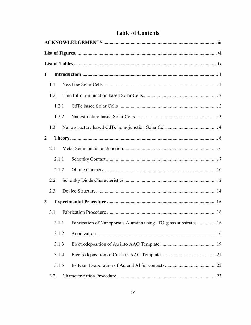
homojunction based solar cell. Such a structure is illustrated in the figure1-1. Such a
structure will have more efficiency due to good lattice matching and losses due to
interfaced states and traps are avoided.
5
Figure 1-1: Device structure of proposed nanostructure based CdTe homojunction
solar cell with illumination from the top
This idea of making a CdTe based homojunction solar cell is the motivation behind this
thesis. This work focuses over the fabrication of Au-n type CdTe Schottky diodes
embedded inside a porous alumina template over ITO-glass. Device and material
characteristics are discussed. Chapter 2 describes the basic theory behind Metal-
Semiconductor junctions and their characteristics. Chapter 3 discusses the experimental
details of Au-CdTe device fabrication and Chapter 4 presents a discussion of results and
observations made. Chapter 5 summarizes the results with the conclusions drawn and
presents suggestions for future research work.

6
2 Theory
2.1 Metal Semiconductor Junction
Although our knowledge of Metal-Semiconductor contacts can be traced as far
back as early work by Braun (1874), it was not until 1938 that both Schottky and Mott
independently suggested a model for the rectification mechanism28
. They pointed out that
the observed direction of rectification could be explained by supposing that electrons
passed over a potential barrier through the normal process of drift and diffusion.
A metal-semiconductor is a junction formed by the intimate contact of a metal
and a semiconductor having non equal work functions. These can be classified as ohmic
or rectifying, depending on the relative work function difference between the metal and
semiconductor and type of the semiconductor used (p-type or n-type). An ohmic contact
is like a typical resistor thus providing a means to connect the semiconductor directly to
outside world with some loss due to the resistance where as a rectifying contact exhibits
diode behavior with a turn-on voltage and diode ideality factor. The only fundamental
difference between a metal-semiconductor Schottky diode to that of a conventional p-n
junction diode is that the majority carriers in the semiconductor dominate the current
incase of metal-semiconductor junction. It can be viewed as a one sided abrupt (e.g., p+ -
n) junction.
The current flow across the metal-semiconductor contacts can take five paths 29-31
.
These are: (i) thermionic emission current from the semiconductor over the potential
barrier into the metal, the dominant process for Schottky diodes with moderately doped
semiconductor operated at a moderate temperature like 300K, (ii) quantum-mechanical
tunneling current through the barrier, the dominant process for contact with a heavily
doped semiconductor, (iii) recombination current in the space-charge region, (iv)
injection current from the metal to the semiconductor and (v) recombination current via
interface states.

7
In a material the work function is defined as the energy difference between the
vacuum level and the Fermi level and is denoted by qΦm or (Φm volts) for a metal and is
equal to q (χ + Vn) or qΦs for a semiconductor where qχ is the electron affinity measured
from the bottom of the conduction band Ec to vacuum level, and qVn is the energy
difference between Ec and the Fermi level. In a metal semiconductor junction the charge
will flow from the semiconductor to the metal and thermal equilibrium is established.
2.1.1 Schottky Contact
A Schottky contact refers to the contact between a metal and a semiconductor
that hinders the flow of carriers in and out of the semiconductor. When negative charges
are brought near the metal surface, positive charges are induced in the metal. This
induced force coupled with an applied electric field, the effective work function is
somewhat reduced. Such lowering of the barrier is referred to as Schottky effect and the
rectifying contacts are referred to as Schottky barrier diodes.
When Φm > Φs, the n-type semiconductor Fermi level is initially higher than that
of the metal before contact is made as shown in the above figure. The Fermi levels on
both sides line up and relative to the Fermi level in the metal, the Fermi level in the
semiconductor is lowered by an equal amount equal to the difference between the two
work functions. In order to align the Fermi levels, the electrostatic potential of the
semiconductor must be raised relative to that of metal. In the Figure 4, after a contact has
been made, a depletion region W is formed near the junction on the n-type semiconductor
side. The positive charge on the n type side due to uncompensated donor ions within W
equals the net negative charge accumulated on the metal.

8
Figure 2-1: Schottky barrier between a metal and an n-type semiconductor with ΦΦΦΦm
> ΦΦΦΦs; (a) band diagrams before contact; (b) equivalent band diagram after the
contact
At thermal equilibrium as the fermi levels align, a contact potential Vo is formed
at the junction. This potential prevents further electron diffusion from the semiconductor
conduction band into the metal. This potential is equal to the difference in the work
function potentials Φm - Φs and the potential barrier height ΦB is Φm - χ where qχ is the
electron affinity measured from the vacuum level to the n type semiconductor band edge.
The equilibrium contact potential Vo can be decreased or increased by applying either
forward or reverse bias voltage just like in p-n junction.
The figure 2-2 describes the energy band diagram for a Schottky barrier on a
metal- p-type semiconductor with Φm < Φs. In this case the fermi level of the metal is

9
higher than that of p-type semiconductor before the contact has been made. Aligning
fermi levels at equilibrium requires a positive charge on the metal side and a negative
charge on the p-type semiconductor side of the junction. In the p-type semiconductor of
the above figure, a depletion width of W is formed near the junction after the contact has
been made. The negative charge due to ionized acceptors within W matches the positive
charge on the metal. The potential barrier Vo prevents further hole diffusion from the
semiconductor into the metal is equal to the difference in the work function of the
semiconductor and metal (Φs - Φm). The potential can be raised or lowered by application
of voltage across the junction just like in the metal-n type semiconductor junction.
Figure 2-2: Schottky barrier between a metal and a p-type semiconductor with ΦΦΦΦm <
ΦΦΦΦs; (a) band diagrams before contact; (b) equivalent band diagram after the contact

10
2.1.2 Ohmic Contacts
An ohmic contact refers to the contact made between a metal and a
semiconductor which allows the carriers to flow in and out of the semiconductor without
any loss at the junction between metal and semiconductor.
Figure 2-3: Ohmic contact between a metal and an n-type semiconductor with
ΦΦΦΦm < ΦΦΦΦs; (a) band diagrams before contact; (b) equivalent band diagram after the
contact
An ideal ohmic contact must be capable of delivering the required current with no
voltage loss between semiconductor and the metal. In reality, an ohmic contact must have
a contact resistance as low as possible and should be negligible when compared to the
bulk resistance of the semiconductor.

11
Figure 2-4: Ohmic contact between a metal and a p-type semiconductor with
ΦΦΦΦm > ΦΦΦΦs; (a) band diagrams before contact; (b) equivalent band diagram after the
contact
Metal-semiconductor contacts are said to be ohmic when the charge induced in
the semiconductor in aligning the fermi levels is provided by the majority carriers. For
example in the case of metal-n type semiconductor junction, the fermi levels are aligned
at equilibrium by transferring electrons from the metal to the semiconductor. This
transferring of electrons raises the electron energy levels in the n type semiconductor
relative to the metal at equilibrium. With Φm < Φs, the barrier to the electron flow
between the metal and the semiconductor is very small and easily overcome by a small

12
voltage. Thus the junction effectively acts as a linear resistor. Conversely for a p type
semiconductor, Φm > Φs results in easy hole flow across the junction. Energy band
diagram of such a junction is illustrated in the figure 2-2 and 2-3.
2.2 Schottky Diode Characteristics
Schottky contact or rectifying contact behaves the same way as a p-n junction
diode. I-V characteristics of a metal-semiconductor junction are similar to that of p-n
junction diode. Thus the diode equation should hold good for I-V characteristics of metal-
semiconductor Schottky junction.
The diode equation is given by
Where Io is the reverse saturation current, V is the applied voltage, k is the Boltzmann’s
constant, T is the temperature and q is the charge of single electron. The reverse
saturation current, Io, is given by
Where A is the area of contact and B is the effective Richardson constant.
On applying a forward bias voltage V to the Schottky barrier of the figure 2-4, the
contact potential reduces from Vo to Vo-V as shown in the following figure. As a result,
electrons in the semiconductor conduction band can diffuse across the depletion region
into the metal thus increasing the forward current through the junction. Conversely on
applying a reverse bias voltage Vr, the contact potential increases from Vo to Vo + Vr, and
electron flow from semiconductor to metal becomes negligible. In this case the forward
current is due to the injection of majority carriers from semiconductor to the metal and
virtually no reverse current exits.

13
The absence of minority carrier injection and the associated storage delay time are
important features of Schottky barrier diodes.
Figure 2-5: Bias characteristics of a metal- n type semiconductor Schottky junction;
(a) Forward bias, (b) Reverse bias
[ote: Most of the theory in section 2.1 and 2.2 has been taken from reference 19 and 23]

14
2.3 Device Structure
The device structure that was investigated is as shown in the figure below.
Figure 2-6: 2 Dimensional view of the cross section of CdTe nanowires based
Schottky diode with Al on top as contact (ohmic) and Au as Schottky contact to
CdTe wire at the bottom
Here Aluminum (Al) and Indium Tin Oxide (ITO) act as cathode and anode
respectively. Cadmium Telluride (CdTe) nanowires (75 nm-85 nm) stand over Gold (Au)
nanowires (10 nm-15 nm), inside the alumina (Al2O3) template over the anode ITO, with
a thin layer (10 nm -15 nm) of TiO2 in between.

15
Figure 2-7: 3 dimensional view of Au-CdTe Schottky diode with Al on top as ohmic
contact
Figure 2-8: 3 dimensional view of Au-CdTe Schottky diode with Au on top as
Schottky contact

16
3 Experimental Procedure
3.1 Fabrication Procedure
The device was fabricated first by preparing the template used by preparing anodized
aluminum oxide (AAO) over ITO-glass, filling it with Au for 15nm - 20nm by
electrodepostion using 2 electrode process followed by electro deposition of CdTe using
3 electrode process and finally evaporating aluminum as top contact.
3.1.1 Fabrication of anoporous Alumina using ITO-glass substrates
Glass ITO substrates are the starting materials for these devices. These substrates
are precoated with 150 nm thick conductive transparent ITO. They are 1” x 1” in size
with a sheet resistance of 4-8 ohms/square. These substrates are first sonicated using an
ultrasonic bath in acetone for 2 minutes in ultrasonicator model 50HT of VWR. The
temperature was set to 30° C during ultrasonication. Then, these substrates are rinsed
with isopropyl alcohol (IPA) and finally sonicated again in de ionized (DI) water for 2
minutes at 30° C in the same ultrasonicator. The cleaned substrates are then dried in
Nitrogen. A thin layer of Titanium (Ti) around 15 nm was vacuum evaporated at a
chamber pressure of ~5.0E-6 torr using Torr International E-beam evaporator. After
deposition, the templates were annealed at 200° C in air. Annealing in air oxidizes Ti to
form TiO2 which acts as a good adhesive conducting layer between Al and ITO. Al was
then vacuum evaporated at a chamber pressure of ~5.0E-6 torr using Torr International E-
beam evaporator with a thickness around 200 nm to 225 nm. Then these samples are
subjected to 2 step anodization process reported by S. Phok et al 34
to obtain highly
ordered patterned pores.
3.1.2 Anodization
The procedure for fabricating anodized aluminum oxide typically consists of an
electro chemical cell with the aluminum substrate as anode, platinum plate (1” x 1”) as
cathode and a magnetic stirrer. The cell is placed on a stirring instrument and the solution
is constantly stirred during anodization. Stirring the electro chemical solution is a critical
step in obtaining ordered pore arrays. The rate of rotation was approximately 45-60 rpm.
The temperature of the electrolyte is maintained at 5° C.
17
The aluminum substrate and platinum plate are then placed into the reaction cell,
with alligator clips securing them. The clips themselves are placed a few millimeters
above the surface of the electrochemical solution. The electro chemical solution used is
0.3 M oxalic acid (C2H2O4). We used potentiostatic anodization for the two steps of
anodization.
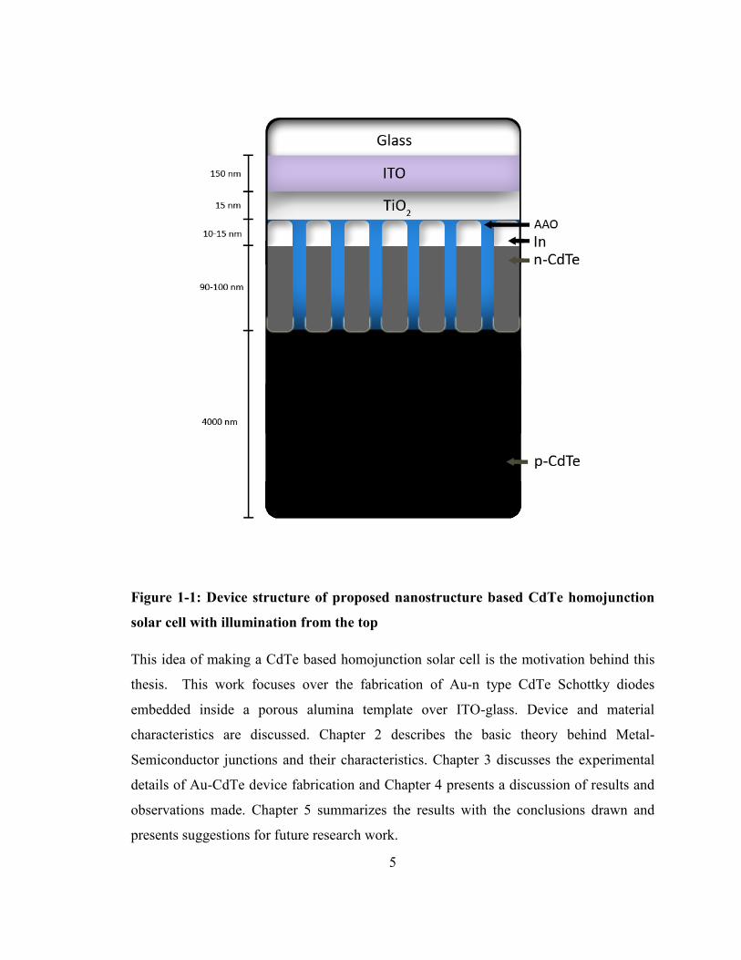
1st step anodization:
During the first step, the maximum potential was set to 25 V and maximum
current to 0.200 amps, cathode was given to platinum plate and anode was given to
aluminum substrate. Anodization was carried for 2 minutes.
Figure 3-1: Current-time and Voltage-time plots during 1st step anodization
As soon as the potential is applied, the current is infinite and so shows the
maximum current of 200 mA. This is because of the conductivity of aluminum initially.
18
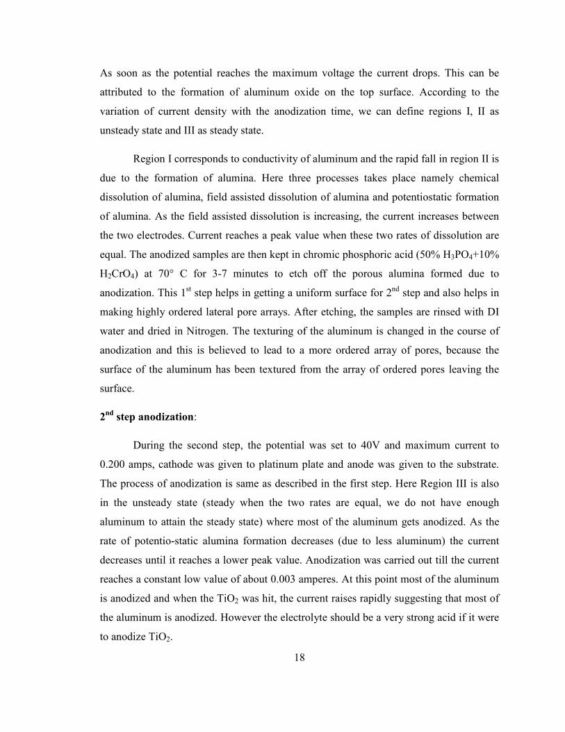
As soon as the potential reaches the maximum voltage the current drops. This can be
attributed to the formation of aluminum oxide on the top surface. According to the
variation of current density with the anodization time, we can define regions I, II as
unsteady state and III as steady state.
Region I corresponds to conductivity of aluminum and the rapid fall in region II is
due to the formation of alumina. Here three processes takes place namely chemical
dissolution of alumina, field assisted dissolution of alumina and potentiostatic formation
of alumina. As the field assisted dissolution is increasing, the current increases between
the two electrodes. Current reaches a peak value when these two rates of dissolution are
equal. The anodized samples are then kept in chromic phosphoric acid (50% H3PO4+10%
H2CrO4) at 70° C for 3-7 minutes to etch off the porous alumina formed due to
anodization. This 1st step helps in getting a uniform surface for 2
nd step and also helps in
making highly ordered lateral pore arrays. After etching, the samples are rinsed with DI
water and dried in Nitrogen. The texturing of the aluminum is changed in the course of
anodization and this is believed to lead to a more ordered array of pores, because the
surface of the aluminum has been textured from the array of ordered pores leaving the
surface.
2nd
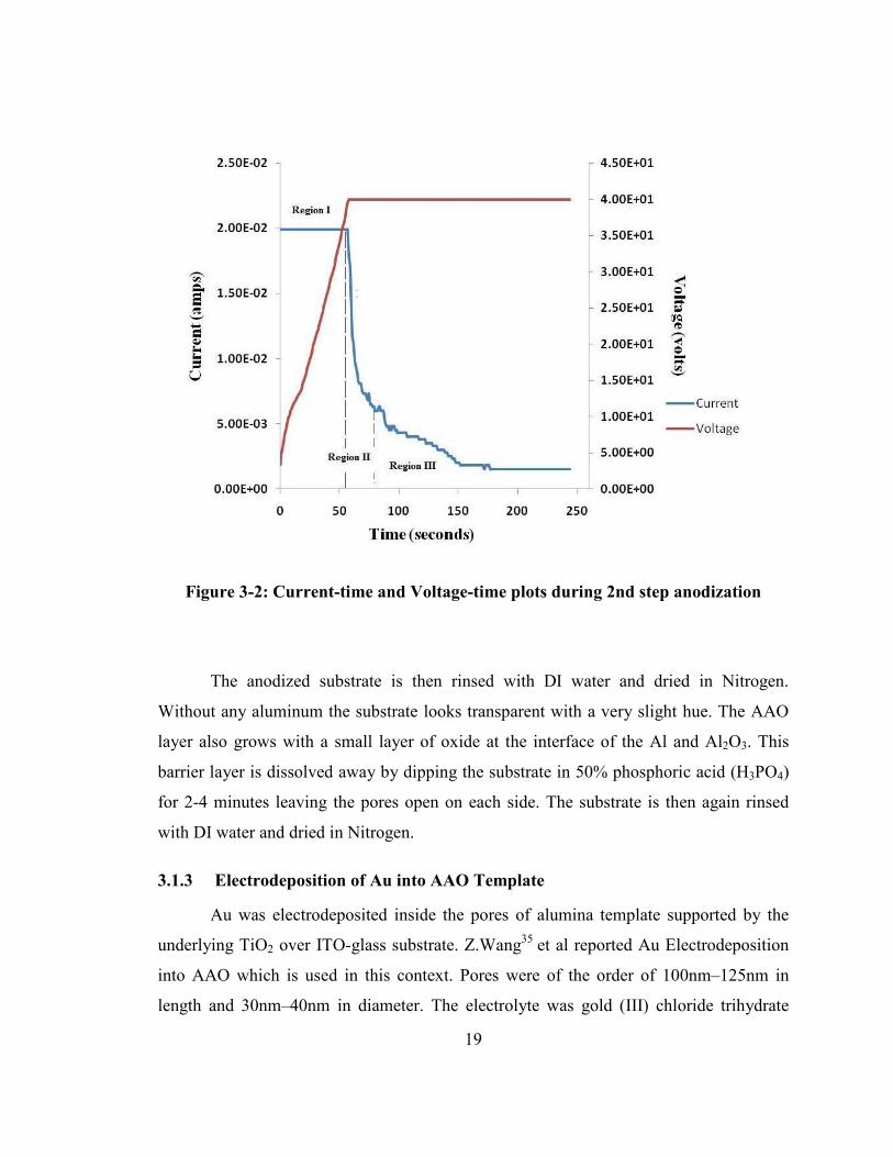
step anodization:
During the second step, the potential was set to 40V and maximum current to
0.200 amps, cathode was given to platinum plate and anode was given to the substrate.
The process of anodization is same as described in the first step. Here Region III is also
in the unsteady state (steady when the two rates are equal, we do not have enough
aluminum to attain the steady state) where most of the aluminum gets anodized. As the
rate of potentio-static alumina formation decreases (due to less aluminum) the current
decreases until it reaches a lower peak value. Anodization was carried out till the current
reaches a constant low value of about 0.003 amperes. At this point most of the aluminum
is anodized and when the TiO2 was hit, the current raises rapidly suggesting that most of
the aluminum is anodized. However the electrolyte should be a very strong acid if it were
to anodize TiO2.
19
Figure 3-2: Current-time and Voltage-time plots during 2nd step anodization
The anodized substrate is then rinsed with DI water and dried in Nitrogen.
Without any aluminum the substrate looks transparent with a very slight hue. The AAO
layer also grows with a small layer of oxide at the interface of the Al and Al2O3. This
barrier layer is dissolved away by dipping the substrate in 50% phosphoric acid (H3PO4)
for 2-4 minutes leaving the pores open on each side. The substrate is then again rinsed
with DI water and dried in Nitrogen.
3.1.3 Electrodeposition of Au into AAO Template
Au was electrodeposited inside the pores of alumina template supported by the
underlying TiO2 over ITO-glass substrate. Z.Wang35
et al reported Au Electrodeposition
into AAO which is used in this context. Pores were of the order of 100nm–125nm in
length and 30nm–40nm in diameter. The electrolyte was gold (III) chloride trihydrate
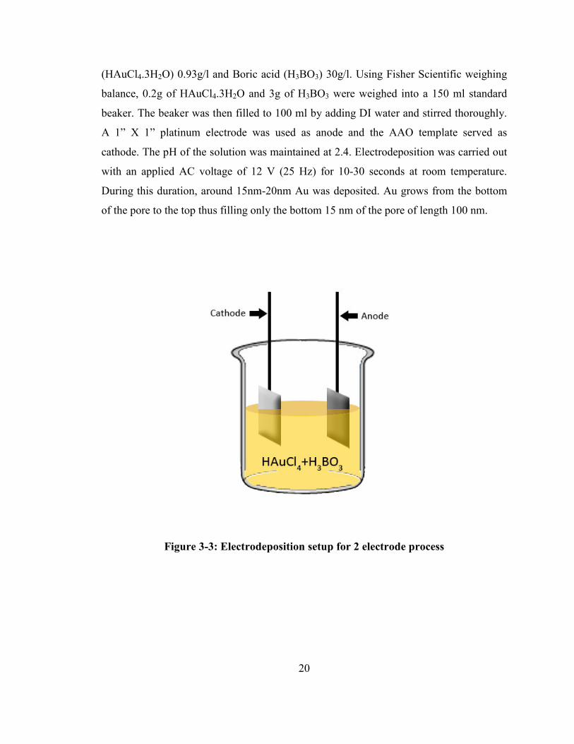
20
(HAuCl4.3H2O) 0.93g/l and Boric acid (H3BO3) 30g/l. Using Fisher Scientific weighing
balance, 0.2g of HAuCl4.3H2O and 3g of H3BO3 were weighed into a 150 ml standard
beaker. The beaker was then filled to 100 ml by adding DI water and stirred thoroughly.
A 1” X 1” platinum electrode was used as anode and the AAO template served as
cathode. The pH of the solution was maintained at 2.4. Electrodeposition was carried out
with an applied AC voltage of 12 V (25 Hz) for 10-30 seconds at room temperature.
During this duration, around 15nm-20nm Au was deposited. Au grows from the bottom
of the pore to the top thus filling only the bottom 15 nm of the pore of length 100 nm.
Figure 3-3: Electrodeposition setup for 2 electrode process

21
3.1.4 Electrodeposition of CdTe in AAO Template
CdTe was electrodeposited inside the pores of alumina template aided by the
underlying Au inside the pores with underlying TiO2 over ITO-glass substrate. After Au
deposition around 70nm-85nm pore length is available for CdTe deposition. The
electrolyte was 1 M Cadmium Sulfate (3CdSO4.8H2O) and 0.15 mM Tellurium (IV)
oxide (TeO2). The electrolyte was first prepared by dissolving TeO2 in concentrated
Sulfuric acid. 4.8 mg of TeO2 was taken in a 20 ml standard beaker. Few drops of
concentrated sulfuric acid (H2SO4) around 2 ml was added to the beaker. 3 ml of DI
water is added and thoroughly stirred.
Figure 3-4: Electrodeposition setup for 3 Electrode process
22
After the solids are completely dissolved, the solution is then added to a standard
beaker of 300 ml. 51.2g of 3CdSO4.8H2O (1 M) was added to the solute followed by DI
water to reach the final volume to 200ml. The solution is thoroughly stirred till all the
solids are completely dissolved and pH was adjusted to 2 by adding few drops of
concentrated H2SO4.
A 1”x1” platinum electrode was used as counter electrode, Au deposited AAO
substrate served as working electrode and Saturated Calomel Electrode was used as
reference electrode. Electrodeposition was carried out at 600 mV against the reference
electrode. The temperature of the electrolyte was maintained at 70° C during the process
of electro deposition. The deposited CdTe nanowires are then annealed in a reducing
environment (95% Ar + 5% H2) for 6 hours at 200° C.
3.1.5 E-Beam Evaporation of Au and Al for contacts
For depositing Au and Al as contacts on the samples a Torr International E-Beam
evaporator was used. The substrate was first masked with Al foil in the form of dots of
crossectional area of 0.07cm2. The masked substrates are placed inside a vacuum
chamber, in which a source of the material to be deposited is placed in a graphite
crucible. The density, z factor, tooling and sense average are set to the respective values
of the material used for deposition. An electron beam (E-beam) is aimed at the source
material causing local heating. The source material is heated to the point that it liquefies,
starts to boil and evaporates. The vacuum is essential to allow the atoms to evaporate
freely in the chamber, and subsequently condense on all surfaces.
23
3.2 Characterization Procedure
Characterization of the device is probably the most important aspect of any
research work. They help the researcher in explaining the properties of the fabricated
device and also help in ascertaining reasons for the cause of failures thereby improving
the conditions to get to the best possible device. The devices and structures fabricated as
a part of thesis primarily relied on the following procedures for characterizations: Field
Emission Scanning Electron Microscopy, Ultraviolet-Visual Absorption Spectroscopy,
X-ray Diffraction Instrument and J-V analysis. The descriptions of procedures of the
above are explained in the following sections.
3.2.1 X-ray Diffraction
X-Ray Diffraction is a technique employed to ascertain the elemental composition
and crystal structure of a particular material under investigation. This is usually done
before any other characterization as it is non-destructive. The principle behind X-ray
diffraction is Bragg’s law (lambda = 2d sine theta). It works by measuring properties of
the scattered X-Ray beam as a function of its angle of incidence, intensity, polarization
and wavelength for a particular material under investigation and comparing it with a
known database kept by the International Center for Diffraction Data. X-Ray diffraction
spectrum is usually plotted as intensity vs. 2θ, where θ is the angle of incidence. Every
known material existing in elemental, alloy, compound form has an X-Ray spectrum
associated with it which is the characteristic of that particular material. Thus, X-Ray
diffraction is typically used to ascertain the quality (or degree of purity) of a particular
substance.
A Bruker-AXS D8 DISCOVER Diffractometer was used to obtain the X-ray
diffraction spectra of all the samples fabricated. The glass substrate with deposited CdTe
nanowires is aligned vertically with respect to the X-ray source and the detector. After
alignment, automated proprietary software was used to obtain the diffraction spectrum for
2θ angle ranging from 10° to 80° of angles of incidence with a step scan of 0.02o.
Patterns thus obtained were cross-referenced with the spectra in the reference database
software for suitable match and identification of compounds present in the sample.
24
3.2.2 Ultraviolet-Visual Absorption Spectroscopy
After ascertaining the phase and crystalline structure of the material deposited, the
samples are taken for absorption spectroscopy. Absorption spectroscopy in the optical
and ultraviolet wavelengths is a non destructive procedure employed to quantitatively
determine the effective band gap shift due to nano wires from that of the bulk
characteristic. This can be calculated using Tauc’s Law. A Cary-50 v3.0 UV-Visual
Spectrophotometer was used to obtain the absorption spectrum of the samples fabricated.
UV-Vis spectroscopy was used to infer the optical properties of the CdTe nanowires
deposited into AAO aided by Au at the bottom and nano crystalline CdTe. Au being a
metal actually reflects the beam but since it is only in the order of 10-15 nm bares very
little effect on the overall spectrum.
3.2.3 Field Emission Scanning Electron Microscopy
A Field Emission Scanning Electron Microscope (FESEM) works by scanning a
high energy electron beam over a sample. Upon hitting the sample, the electron beam
generates secondary electrons, back-scattered electrons and X-rays. These are collected
by a collector to report qualitative and quantitative information about the sample being
studied. Typically such information involves a detailed topographic view of the sample
and the elemental content at a particular location on the sample. A Hitachi FESEM
(Model S-900) with a maximum magnification power of 800kX at an accelerating
potential of 3kV was used for characterization purposes for this thesis work.
To image a particular sample, a very small section of the sample was cut-off from
the original sample and mounted on a 2mm x 5 mm double-sided sticky carbon tape stuck
on a small copper stub. A very small thickness of Gold-Palladium alloy was sputter
coated to ensure proper electrical conductivity throughout the sample. Samples were
typically imaged at 3kV to get the best resolution. Samples were imaged for both
topology as well as cross-sectional views. During the cross-sectional view the sample is
tilted at an angle of 30°, at this angle the image so viewed will be half the actual size
(Sine 30° =0.5).

25
3.2.4 J-V characterization and analysis
Current density-voltage (JV) measurements usually become the major
accomplishment of any characterization procedure as they are the motivation behind any
fabrication. The JV plots give us a raw picture of how the currents are flowing as a
function of applied potential in dark as well as under illumination. They also give us
valuable information regarding series resistance (Rs), shunt resistance (Rsh), diode
ideality factor (η), diode saturation current (Io), short circuit current (Isc), open circuit
voltage (Voc), maximum power point (Pm), fill factor and conversion efficiency39
. The
equipment for measuring JV consisted of a Kepco programmable bipolar operational
amplifier/power supply (Model BOP 36-12M) and two Keithley digital multimeters
employed as voltmeters (Model 2001 and 2000) interfaced with a common lab PC using an
application software developed in-house with LabVIEW Student Edition 7.0 provided by
National Instruments. The supply voltages are varied from -1V to +2V in steps of 0.05V.
Corresponding current values are measured, converted to appropriate current density and
logged in the form of .txt files by the LabVIEW software program. A subsequent plot of
these values in Microsoft excel generated the JV plots from which other parameters were
calculated. During the dark condition, all the lights are switched off and during illumination a
light source of 1 sun is directed on the sample from top.

26
4 Results and Discussion
4.1 Electro deposition of CdTe inside AAO template over ITO-glass
The Current-Time plot against the working electrode with respect to counter
electrode is shown below.
0.00E+00
5.00E-04
1.00E-03
1.50E-03
2.00E-03
2.50E-03
0 100 200 300 400 500 600 700 800 900 1000
Time(seconds)
Cu
rren
t(am
ps)
Figure 4-1: Current-Time plot against working electrode with respect to counter
electrode during Electro-deposition of CdTe
The pores were of the length 100nm long with 15nm -20nm of Au at the bottom.
This leaves a space of around 75nm – 80nm. Near stoichiometric CdTe nanowires were
formed at a potential of -600 mV across reference voltage. This is applied across working
electrode (substrate) and reference electrode (Saturated Calomel Electrode). At this point

27
the voltage across counter electrode (platinum plate) and working electrode was 2.58 V
suggesting the approximate potential required to implement the same in a 2 electrode
setup. But the need to get CdTe in exact stoichiometry, we had to switch to 3 electrode
setup as the variance in such as a set up is only 20-25 mV whereas in a 2 electrode setup
would be more than 100 mV. As we can observe from the graph that current suddenly
dropped from a peak of 1.95 mA when time reached 640 seconds. This could be as a
result of pores being filled. The rate of deposition is approx 10nm/min. Panicker et al29
pioneered deposition of CdTe on a thin film. It consists of two elementary steps:
HTeO2+ + 3H
+ + 4e
- Te(s) + H2O
E0 = 0.55V vs NHE (1)
Cd2+
+ Te(s) + 2e- CdTe(s)
E0 = 0.10V vs NHE (2)
where NHE is Normal Hydrogen Electrode,
It was observed that at higher potential synthetic cadmium was deposited and at
higher pH synthetic tellurium was deposited. M C Kum et al 27
reported an extensive
study of the various reactions taking place with respect to pH and deposition potential.
28
4.2 Characterization of CdTe nanowires using Scanning Electron Microscopy
(SEM)
Figure 4-2: Cross section of a typical AAO template over ITO glass
The cross section of a typical AAO template over ITO glass is shown in the figure
4-2. Layers of Glass, ITO, and TiO2 along with AAO pores standing on the top of these
layers are also shown. As we can see the pores are uniformly distributed. The SEM
images of electro deposited CdTe nanowires inside the AAO template on ITO are shown
in the figure 4-3. The left side of the image (Figure a) is the top surface of the template
showing deposited CdTe inside the pores. Figure b shows a bundle of CdTe nanowires
sitting on top of the template.
AAO
ITO
TiO2

29
Figure 4-3: SEM micrographs (a) top view and (b) top view showing a bundle of
nanowires on top
In the experiments, it was observed that CdTe nanowires grow from the bottom of
the pore aided with Au at the bottom. We observe that some pores are completely filled
and some are not completely filled depending upon the amount of Au deposited in
respective pores prior to the deposition of CdTe. With the duration of deposition, the
pores are etched away partially. This can be attributed to the fact that the electrolytic
solution being highly acidic with pH=2 and at elevated temperature of deposition at 70
oC, the sulfuric ions in the solution starts etching away the pores. This made the
limitation of using AAO template of only 100 nm-200 nm in length for growing CdTe
nanowires. In the 2nd
figure a bundle of nanowires were etched off the pore (and annealed
at the top).
(a) (b)

30
Figure 4-4: Cross section of CdTe nanowires deposited on AAO/ITO
When we do the cross section in scanning electron microscope we tilt the sample
at an angle of 30o, this means that whatever cross section we measured is half the actual
length since sine (30o) = 0.5. The cross section of the electro deposited CdTe
nanowires is shown in the figure 4-4. CdTe nanowires are very small of the order of 70
nm-100 nm and that made it really difficult to make out the nanowires on the cross
sectional (35nm-50nm) images taken from scanning electron microscope. The above
image also shows couple of CdTe nanowires that have fallen out of the cross section due
to the stress produced during the process of breaking the device and mounting it on the
stub.

31
Figure 4-5: SEM micrographs of nanocrystalline CdTe: (a) top view and (b) a closer
view on the top
When the experiment was carried out for a longer duration, the pores were
completely etched off. Although the pores were etched off there was parallel growth of
CdTe wires which after annealing exhibited nano crystalline CdTe. Figure 4-5 shows the
top view of the nano crystalline CdTe. Annealing was done at 200 o
C in Ar for 6 hours.
The images showed cluster like structure with a grain size of nearly 10 nm.
(a) (b)
32
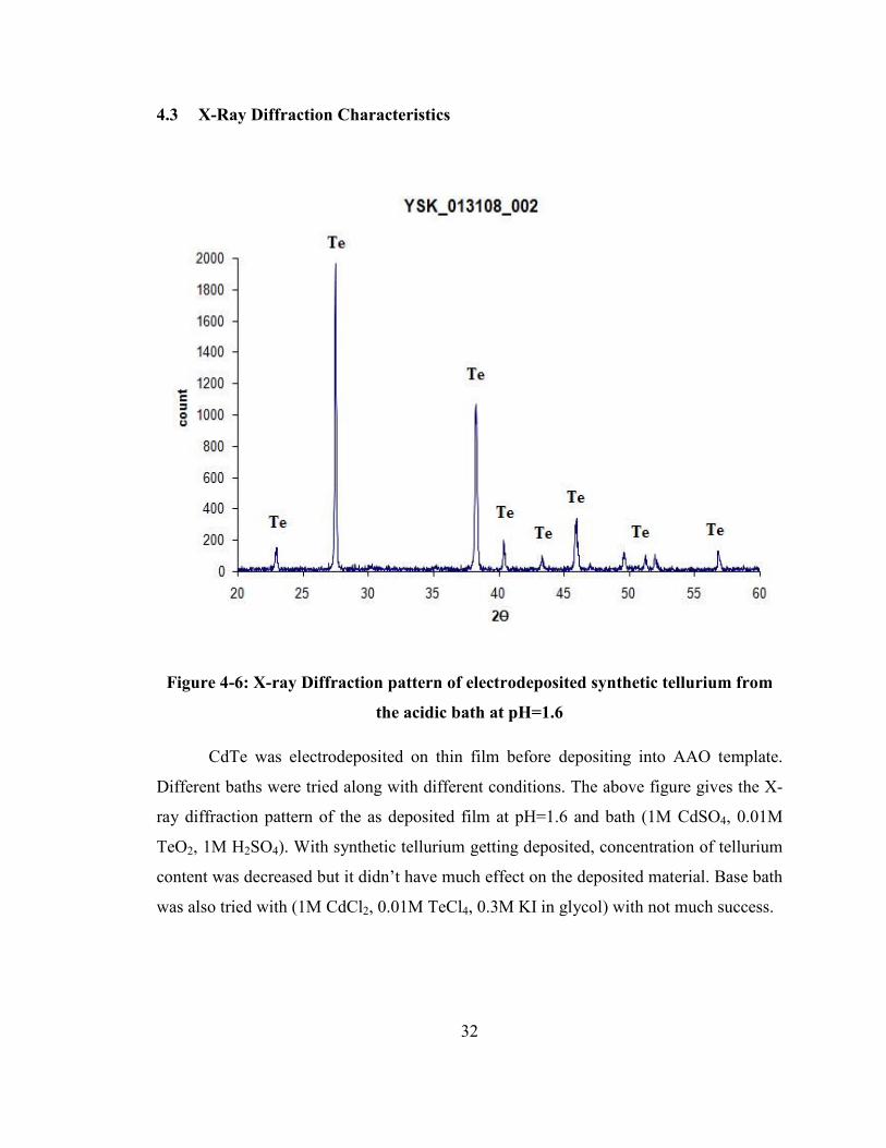
4.3 X-Ray Diffraction Characteristics
Figure 4-6: X-ray Diffraction pattern of electrodeposited synthetic tellurium from
the acidic bath at pH=1.6
CdTe was electrodeposited on thin film before depositing into AAO template.
Different baths were tried along with different conditions. The above figure gives the X-
ray diffraction pattern of the as deposited film at pH=1.6 and bath (1M CdSO4, 0.01M
TeO2, 1M H2SO4). With synthetic tellurium getting deposited, concentration of tellurium
content was decreased but it didn’t have much effect on the deposited material. Base bath
was also tried with (1M CdCl2, 0.01M TeCl4, 0.3M KI in glycol) with not much success.

33
Figure 4-7: X-ray diffraction pattern of electrodeposited CdTe from modified acidic
bath at pH=2.4
From the figure 4-7, we can observe that the electrodeposited sample had more
synthetic cadmium. At pH=2.4 and bath (1M CdSO4, 0.001 M TeO2) CdTe along with
synthetic Cd was observed. This film was tried to type convert into p-type CdTe by
annealing the sample in cadmium rich environment at 450o
C. The CdTe layer peeled off
after annealing.
ITO

34
5
10
15
20
25
30
35
40
45
50
55
15 20 25 30 35 40 45
2Ө
co
un
t
Figure 4-8: X-ray Diffraction pattern of electrodeposited CdTe nanowires in AAO
template on a glass-ITO substrate
CdTe nanowires were oriented vertically within the AAO template during the
XRD scans. Near stoichiometric CdTe nanowires were electrodeposited at -0.600 V. The
x-ray diffraction pattern of the as deposited nanowires (above figure) showed
nanocrystalline cubic phase structures. Two diffraction peaks at 2θ values of 23.8o and
38.2o correspond to (111) and (220) respectively were observed. In the figures, the XRD
peaks of ITO at 2θ values of 21.3o, 30.2
o, 35
o were also observed. The peak at 27.2
o
corresponds to rutile phase of TiO2.
ITO
CdTe
CdTe
ITO
TiO2
ITO
35
Figure 4-9: X-ray diffraction pattern of electrodeposited CdTe nanowires in AAO
template on a ITO-glass substrate annealed at 200oC for 6 hours in a reducing
environment (5%H2+95%Ar)
The as deposited CdTe nanowires were annealed at 200oC for 6 hours in a
reducing environment (5% H2 + 95% Ar). This increased the crystallinity of the
nanowires. As we can observe the intensity of the peaks increased. In the figure 4-9, the
XRD peaks of ITO at 2θ values of 30.2o, 35
o and 60
o were observed. The peaks at 23.8
o,
31.8, 39.1 o
, 46.5 correspond to (111), (112), (220), and (311) respectively.

36
Table1: Phase formation of CdTe with varying concentrations of acidic bath
Tellurium Content Volume of
Conc H2SO4
pH of
the bath
Peak observed
in XRD
0.01 M 4 ml 1.6 Synthetic Tellurium
0.01M 8 ml 2.4 Synthetic Tellurium and CdTe
0.001M 6 ml 2.0 CdTe
4.4 Optical Absorption
Figure 4-10 shows the optical absorption curves for 100nm and nano crystalline
CdTe.
3.50E-01
8.50E-01
1.35E+00
1.85E+00
2.35E+00
300 350 400 450 500 550 600 650 700 750
Wavelength(nm)
Inte
ns
ity
(au
)
YSK_CdTeNW_092708 YSK_CdTeNW_091708
Figure 4-10: Optical absorption spectra of electrodeposited CdTe nanowires
embedded in an AAO template on a glass-ITO substrate

37
We can observe that there is a shift in the absorption peak from 830 nm in bulk to
535 nm in nanowires. Thus the band gap increased from 1.44 eV in bulk to 2.31 eV in
nanowires.
From the figure 4-11, we can observe that nano crystalline CdTe doesn’t have
significant shift in the absorption peak. The shift in the absorption peak of CdTe nano
wires makes them a suitable window layer in the typical solar cell structure of CdS/CdTe
replacing CdS. Nano CdTe thus provides a good window layer and could make a homo
junction with bulk CdTe.
1.20E+00
1.40E+00
1.60E+00
1.80E+00
2.00E+00
2.20E+00
2.40E+00
2.60E+00
350 400 450 500 550 600 650 700
Wavelength (nm)
Inte
ns
ity
(a
u)
Figure 4-11: Optical absorption spectra of electrodeposited nano crystalline CdTe
Fig 4-11 shows the optical absorption spectra of electrodeposited nano crystalline
CdTe. The absorption peak only shifted from 826 nm to 630 nm resulting in a band gap
shift from 1.44eV to 1.96eV. Although nano crystalline CdTe exhibited a band gap shift,
this cannot be used for replacement of bulk CdS. This is because the device was annealed

38
at 200o C. With increase in temperature of annealing, the grain size would have increased
and this band gap shift wouldn’t have been resulted.
4.5 JV Characteristics
4.5.1 JV Characteristics of Au-CdTe Schottky junction inside AAO with Au on
top as contact
The current density (J) vs. Voltage (V) characteristics for Au-CdTe-Au and Au-CdTe-Al
were measured and analyzed.
Figure 4-12: JV characteristics of Au-CdTe-Au with Au-CdTe junction inside AAO
template
39
In the figure 4-12 we observe that currents are very low. This can be attributed to
the fact that n-CdTe makes a Schottky contact with Au at the bottom of the pore and to
the Au at the top contact. With Schottky junctions at the top and the bottom, this structure
makes a back to back diode. Thus confirming that the electro deposited CdTe is n type
which makes a Schottky contact with Au and ohmic contact with Al.
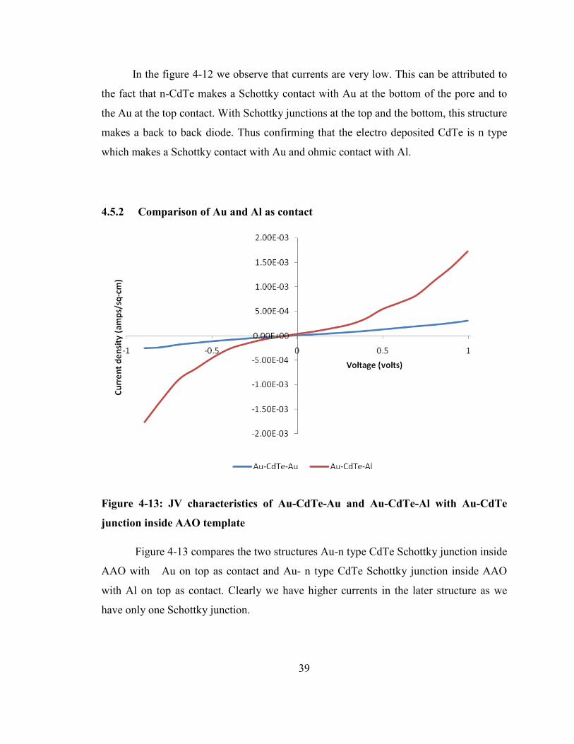
4.5.2 Comparison of Au and Al as contact
Figure 4-13: JV characteristics of Au-CdTe-Au and Au-CdTe-Al with Au-CdTe
junction inside AAO template
Figure 4-13 compares the two structures Au-n type CdTe Schottky junction inside
AAO with Au on top as contact and Au- n type CdTe Schottky junction inside AAO
with Al on top as contact. Clearly we have higher currents in the later structure as we
have only one Schottky junction.
40
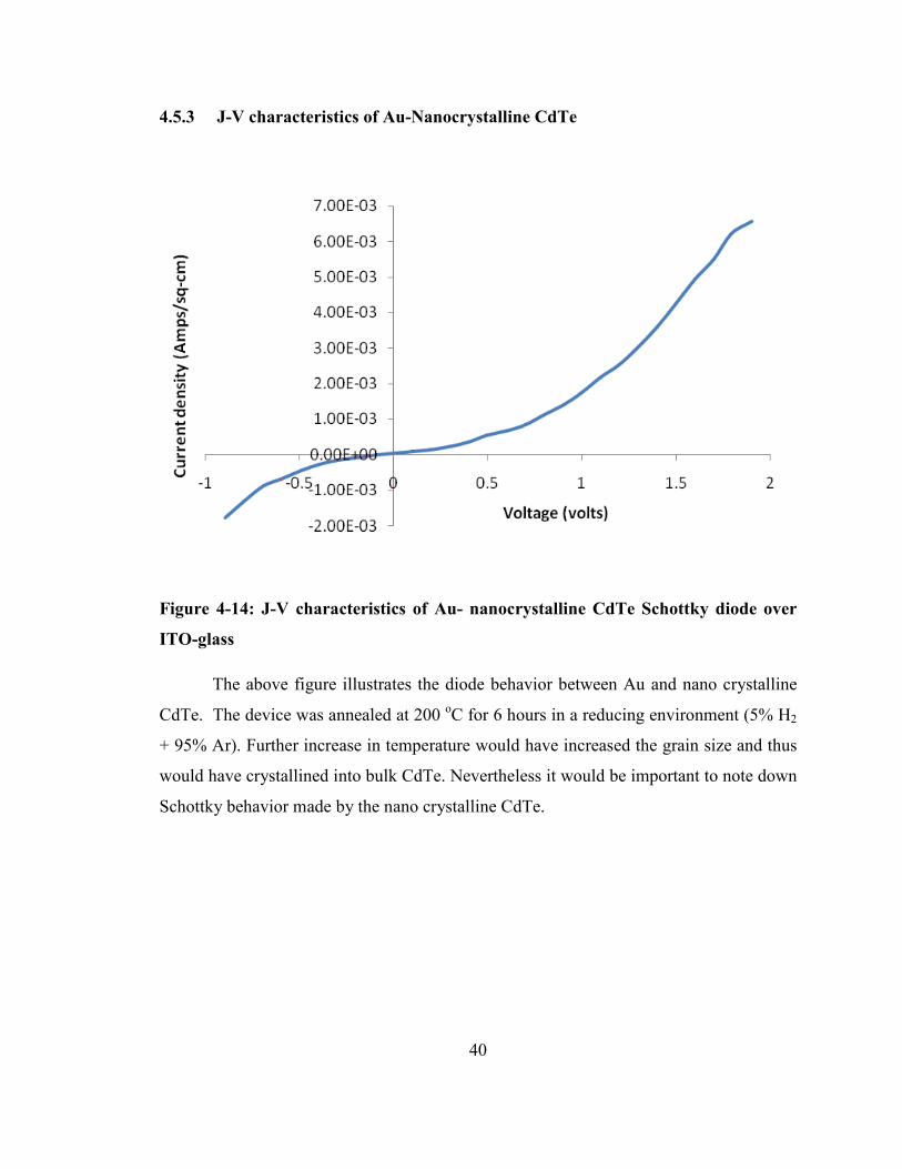
4.5.3 J-V characteristics of Au-anocrystalline CdTe
Figure 4-14: J-V characteristics of Au- nanocrystalline CdTe Schottky diode over
ITO-glass
The above figure illustrates the diode behavior between Au and nano crystalline
CdTe. The device was annealed at 200 oC for 6 hours in a reducing environment (5% H2
+ 95% Ar). Further increase in temperature would have increased the grain size and thus
would have crystallined into bulk CdTe. Nevertheless it would be important to note down
Schottky behavior made by the nano crystalline CdTe.
41
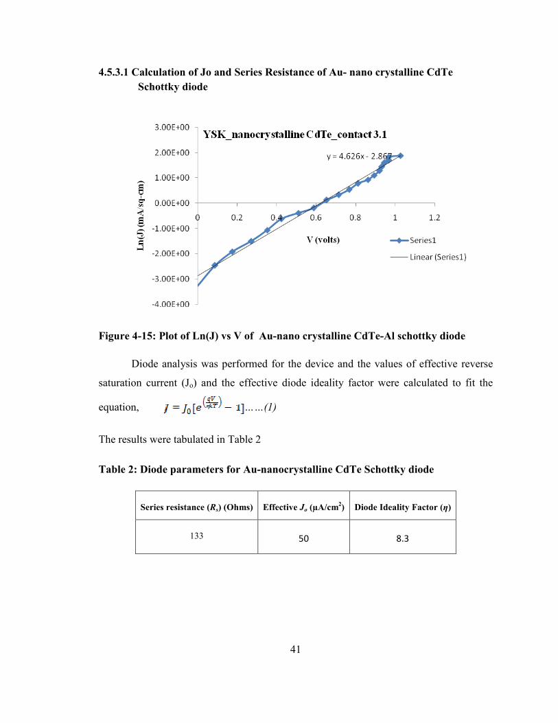
4.5.3.1 Calculation of Jo and Series Resistance of Au- nano crystalline CdTe
Schottky diode
Figure 4-15: Plot of Ln(J) vs V of Au-nano crystalline CdTe-Al schottky diode
Diode analysis was performed for the device and the values of effective reverse
saturation current (Jo) and the effective diode ideality factor were calculated to fit the
equation, ……(1)
The results were tabulated in Table 2
Table 2: Diode parameters for Au-nanocrystalline CdTe Schottky diode
Series resistance (Rs) (Ohms)
Effective Jo (µA/cm2)
Diode Ideality Factor (η)
133
50
8.3

42
4.5.4 J-V Characteristics of 100nm Au-CdTe-Al
Figure 4-16: J-V characteristics of Au-CdTe Schottky diode inside 100 nm long
AAO template over ITO-glass
The current density (J) vs voltage (V) characteristics of Au-CdTe Schottky diode
embedded inside a100nm long AAO template over ITO-glass is shown in the figure 4-16.
The J-V characteristics were also measured under one sun illumination to see if the
device exhibited photovoltaic effect.
It can be seen that the device current is higher under illumination when compared
to their corresponding dark currents owing to photo conductance of CdTe. This can be
attributed to the fact that under illumination more carriers get excited and so more
current.

43
4.5.4.1 Calculation of Jo and Series Resistance of 100nm Au-CdTe Schottky
Figure4-17: Plot of Ln(J) vs V of 100nm Au-CdTe-Al Schottky diode under dark
Figure 4-18: Plot of Ln(J) vs V of 100nm Au-CdTe-Al schottky diode under
illumination

44
Photo conductance was exhibited by the device but no photo voltaic effect was
observed. Diode analysis was performed for the device and the values of effective reverse
saturation current (Jo) and the effective diode ideality factor were calculated to fit the
equation,
……(1)
The results were tabulated in Table 3.
Table 3: Diode parameters for 100nm Au-CdTe-Al Schottky diode
Illumination Series resistance (Rs) (Ohms) Effective Jo (µA/cm2) Diode Ideality Factor (η)
Dark 117.8 34 10.03
Light 110.5 39 10.08
4.5.5 Calculation of Resistivity (ρ) of deposited CdTe nanowires
The Sputtered Aluminum dots have an area of 0.07 cm2. From the SEM images
we can find the pore density to be approximately 1.3E09 pores/cm2. The diameters of the
nanopores were approximately 40nm. So the area of each wire would be 1.256E-11 cm2.
Assuming 20% porosity we have,
45
Figure 4-19: 3-dimensional view of the cross section with corresponding Al contact
Area of the aluminum dot= 0.07 cm2;
Length of the pore = 100 nm;
Radius of the pore= 20 nm;
Area of the pore = π * R2= 3.14 * 20E-9 * 20E-9 = 1.256E-11 cm
2;
Pore density = 1.3E9 pores/cm2;
Porosity= 20%;
Number of CdTe Nanowires in contact with aluminum dot= area of dot * pore density *
porosity
= 0.07 cm2
* 1.3E9 * 0.02 = 1.932E6 nanowires;
Area of CdTe nanowires contact to the metal = Area of the pore * number of CdTe
nanowires
= 1.256E-11 * 1.932E6 = 2.426 E-5 cm2;
We know that resistivity (ρ) = Resistance * Area/ Length
Substituting average series resistance, area of the CdTe nanowires contact, length of the
pore in the above equation, we get
ρ =277 Ωcm.

46
Resistivity of n type CdTe nanowires is found to be 277 Ωcm.
4.6 Calculating Intrinsic barrier potential Vbi
From Fig 2-6 (a) we have work function of Au = 5.1 eV, band gap of CdTe
nanowires from experimental results is 2.31 eV; electron affinity of CdTe nanowires is
3.54 eV36
.
We know conductivity σ = 1/ρ;
From the observed J-V plots we have ρ = 278 Ωcm.
We know σ= 1/µnqn…… (1) Where µn is the mobility of the electron,
q is the charge of the electron,
n is the concentration of electrons in the conduction band.
Also we have n= Nc exp [-(Ec-Ef)/kT] ….. (2) Where Ec is the conduction band edge,
Ef is the Fermi energy level,
k is the Boltzmann constant,
And T is the temperature in Kelvin scale.
From the above two equations we can deduce
Ec - Ef = kT ln (Nc/n)……. (3)
Also Nc = 2(2π mn*
kT/h2)3/2
… (4)Where mn*
is the density of states effective mass for
electrons, in case of CdTe it is 0.10 mo.
Substituting the respective values we get Ec - Ef = 0.676eV.
From the band diagram, work function (Φs) of n type CdTe nanowires is
qχ + Ec - Ef = 4.216 eV,
Thus Vbi is Φm - Φs = 0.884 eV.
47
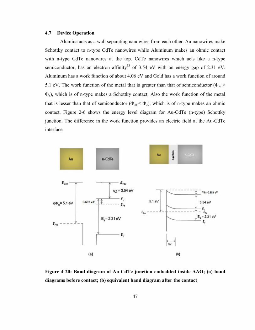
4.7 Device Operation
Alumina acts as a wall separating nanowires from each other. Au nanowires make
Schottky contact to n-type CdTe nanowires while Aluminum makes an ohmic contact
with n-type CdTe nanowires at the top. CdTe nanowires which acts like a n-type
semiconductor, has an electron affinity33
of 3.54 eV with an energy gap of 2.31 eV.
Aluminum has a work function of about 4.06 eV and Gold has a work function of around
5.1 eV. The work function of the metal that is greater than that of semiconductor (Φm >
Φs), which is of n-type makes a Schottky contact. Also the work function of the metal
that is lesser than that of semiconductor (Φm < Φs), which is of n-type makes an ohmic
contact. Figure 2-6 shows the energy level diagram for Au-CdTe (n-type) Schottky
junction. The difference in the work function provides an electric field at the Au-CdTe
interface.
Figure 4-20: Band diagram of Au-CdTe junction embedded inside AAO; (a) band
diagrams before contact; (b) equivalent band diagram after the contact

48
5 Conclusions and Future work
The template-directed electrodeposition method was utilized to electro deposit
CdTe nanowires inside an AAO template over ITO glass. The pH of the bath strongly
influenced the composition of nanowires with near stoichiometric CdTe nanowires
formed at a pH of 2. CdTe nanowires annealed at 200oC in a reducing environment for 6
hours showed improved crystallinity with a strong preference in [111] direction. Gold
was electro deposited to make a Schottky diode inside AAO template with Aluminum
serving as the top ohmic contact. Comparison of J-V characteristics of Au-CdTe-Au and
Au-CdTe-Al revealed that first was a back-to-back diode and second was a normal
Schottky diode. This confirms that the CdTe in the AAO pores was n-type27
. Electrical
characterization of CdTe nanowires revealed a typical S-shaped J-V curve of a
semiconductor due to Schottky barrier height. Illumination under “one sun’ resulted in
higher currents attributed to the photo conductivity of CdTe and the reduction in junction
barrier potential at the Au-CdTe interface. A longer duration of deposition yielded nano
crystalline CdTe and corresponding J-V characteristics were analyzed.
The future work can be focused on electro-depositing indium first followed by CdTe
inside the 100nm and achieve an ohmic junction inside the pore. With bulk p type CdTe
on top, this would result in a homo junction based solar cell which is the motivation
behind this work.

49
References:
1. R. Smalley, “Our Energy Challenge,” presented at the 31st
IEEE PVSC, 1/3/2005,
Walt Disney World, FL.
2. N. S. Lewis, “Scientific Challenges in the Development of Sustainable Energy,”
presented at the 31st
IEEE PVSC, 1/3/2005, Walt Disney World, FL.
3. Scott D. Feldman, “ FUNDAMENTAL ELECTRO-OPTICAL STUDIES OF CdTe
SOLAR CELLS”, thesis
4. http://en.wikipedia.org/wiki/Photovoltaics.
5. Wim C. Sinke ,The Photovoltaic Challenge
6. Kim W. Mitchell “STATUS OF NEW THIN-FILM PHOTOVOLTAIC
TECHNOLOGIES Solar Energy Research Institute, Golden, Colorado 80401
7. S.P.Albright, V.P singh and J.F. Jordan, Sol. Cells, 24 (1988) 43-56.
8. T. Aramoto, S. Kumazawa, H. Higuchi, T. Arita, S.Shubutani, T. Nishio, J. Nakajima,
M. Tsuji, A. Hanafusa, T. Hibino, K. Omura, H. Ohyama and M.Murozono, Jpn.J.
Appl. Phys., Part1 (Regular papers, short notes & Review papers), 36 (1997) 6304-
6305.
9. H.Chavez, R. Santiesteban, J.C. McClure and V.P. Singh, J. Mater. Sci.:Mater.
Electron., 6 (1995) 21-24.
10. http://www.firstsolar.com
11. http://en.wikipedia.org/wiki/Solar_cell
12. Hirshman, William P; Hering, Garret; Schmela, Michael (March 2008), "Market
Survey: Cell & Module Production 2007", Photon International: 140–174
13. D.L. Linam, V.P. Singh, G.B. Lush, E.Clark and G.W.Thompson and E. Clark, Sol.
Energy Mater. Sol. Cells, 59 (1999) 145-161.
14. H. Chavez, M. Jordan, J.C. McClure, G.Lush and V.P. Singh, J. Mater. Sci.: Mater.
Electron, 8 (1997) 151-154.
15. Rangari, V.K.; Sanagapalli, S.; Jayaraman, V.; Mahendra, S.; Singh, V.P. Source:
Solar Energy Materials and Solar Cells, v 82, n 1-2, May 1, 2004, p 315-330

50
16. Singh V.P, Singh R.S., Simpson K. 2006 anostructured Materials for Solar Energy
Conversion ed Tetsuo Soga (Amsterdam: Elsevier) p 167
17. R. Noufi and K. Zweibel Presented at the 2006 IEEE 4th
World Conference on
Photovoltaic Energy Conversion (WCPEC-4).
18. A.P. Alivisatos, J.Phys. Chem., 100 (1996) 13226-13239.
19. M.P.R. Panicker, M. Knaster, F.A. Kroger, J. Electrochem. Soc. 125 (1978) 566.
20. Kuno M Ahmad O Protasenko V, Bacinello D and Kosel T H 2006 Chem. Mater. 18
5722-32.
21. Yang Q, Tang K, Wang C, Qian Y and Zhang S 2002 J.Phys, Chem, B 106 9227-30.
22. Tang Z, Kotov N A and Giersig M 2002 Science 297 237-240
23. Xu D, Chen D, Xu Y, Shi X, Guo G, Gui L and Tang Y 2000 Pure Appl. Chem. 72
127-35.
24. Zhao A W, Meng G W, Zhang L D, Gao T, Sun S H and Pang Y T 2003 Appl. Phys.
A 76 537-9
25. Ohgai T, Gravier L , Hoffer X and Ansermet J P 2005 J. Appl. Electrochem 35 479-
85.
26. Sima M, Enculescu I, Trautmann C and Neumann R 2004 J. Optoelectron. Adv.
Mater 6 121-5
27. Maxwell C Kum, Bong Young Yoo, Young Woo Rheem, Krassimir N Bozhilov,
Wilfred Chen, Ashok Mulchandani and Nosang V Myung. Nanotechnology 19 (2008)
325711 (7pp).
28. Sze S.M. and Ng Kwok K., 2007 Physics of semiconductor devices, Third edition,
John Wiley, 157
29. V.P Singh, O.M Erickson and J.H. Chao, J.Appl. Phys., 78 (1995) 4538-4542.
30. O.M.Erickson, J.C. McClure and V.P.Singh, Proc. 6 Int. Photovoltaic Sci.Eng Conf.,
(1992) 97.
31. D.L.Linam, V.P.Singh, J.C. McClure, G.B.Lush, X.Mathew and P.J. Sebastian, Sol.
Energy Mater. Sol. Cells, 70 (2001) 335-344.

51
32. Ben G. Streetman and Sanjay Banerjee., 2000 Solid State Electronic devices, Fifth
edition, Prentice hall, 85.
33. P.Von Huth, J.E. Butler, W.Jaegermann, and R. Tenne, ECS, 149 (1) G55-G62
(2002).
34. Phok S., Rajaputra S., Singh V.P. 2007 anotechnology 18 475601.
35. Z.Wang, Y.-K. Su, and H.-L. Li., Appl. Phys. A 74, 563–565 (2002).
36. Jin-Hyoung Kim, Hyunsuk Kim, Kyoungah Cho, Dong-Young Jeong and Sangsig
Kim, Japanese Journal of Applied Physics, Vol. 45, No. 2A, 2006, pp. 1033-1039.
37. V.P. Singh, D.L.Linam, D.W. Dils, J.C.McClure, G.B.Lush, Solar energy materials
and solar cells 63 (2000) 445-466.
38. R. K. Sharma, Kiran Jain and A. C. Rastogi, Current Applied Physics, 3, p199-204
(2003).
39. Shounak Mishra, “SCHOTTKY DIODES O CADMIUM SULFIDE (CdS) AOWIRES
DEPOSITED I POROUS ALUMIA TEMPLATES”, Master’s Thesis, University of
Kentucky (2007)

52
Vita
Srikanth Yanamanagandla was born in Mahabubnagar, Andhra Pradesh, India on
December 6th
, 1984. He received his Bachelor of Technology degree in Electronics and
Communication Engineering in 2006 from Jawaharlal Nehru Technological University,
Hyderabad, India. He worked as a Research Assistant from 2007-2008 in the Electronic
Devices Research Group at the University of Kentucky, Lexington, Kentucky, U.S.A.
______________________
Srikanth Yanamanagandla