Synchrotron Radiation and Materials Science Applicationsattwood/srms/2007/Lec16.pdf · Learning...
55
Synchrotron Radiation and Materials Science Applications X-Ray Diffraction for Materials Science Application 203 McLaughlin Hall March 13, 2:10 to 3:30 pm Simon Clark Advanced Light Source, LBNL and UCB E&PS
Transcript of Synchrotron Radiation and Materials Science Applicationsattwood/srms/2007/Lec16.pdf · Learning...
Synchrotron Radiation and Materials Science Applications
X-Ray Diffraction for Materials Science Application
203 McLaughlin Hall March 13, 2:10 to 3:30 pm
Simon ClarkAdvanced Light Source, LBNL and UCB E&PS

Learning objectives
1. Understand the advantages of a synchrotron source of x-ray diffraction2. Understand the differences between single crystal and powder diffraction3. Understand the differences between monochromatic and polychromatic
diffraction4. Appreciate the use of these techniques in investigating material science
problems

Presentation plan
1.Why use synchrotron radiation?2.Single crystal diffraction
1.Polychromatic2.Monochromatic
3.Powder diffraction1.Monochromatic2.Polychromatic
Acknowledgements
Nobumichi Tomura MicrodiffractionSimon Teat Single crystal diffractionLyn McClusker Powder build up

Why use a synchrotron for diffraction?
• High Brightness• Highest resolution• Smallest samples
• Continuous spread of wavelengths• Laue diffraction
• High energy (short wavelength)• High penetration, in-situ studies
• High intensity• Time resolved studies

Presentation plan
1.Why use synchrotron radiation?2.Single crystal diffraction
1.Polychromatic2.Monochromatic
3.Powder diffraction1.Monochromatic2.Polychromatic

Laue or monochromatic?
λ = 2d sin θ

Pros and cons of Laue and Bragg?
Laue (polychromatic)• One shot experiment• Difficult to make intensity corrections• Overload problem
Bragg (monochromatic)• Takes many frames to get complete data set

Presentation plan
1.Why use synchrotron radiation?2.Single crystal diffraction
1.Polychromatic2.Monochromatic
3.Powder diffraction1.Monochromatic2.Polychromatic

La0.95Sr0.05Ga0.90Mg0.10O3-x
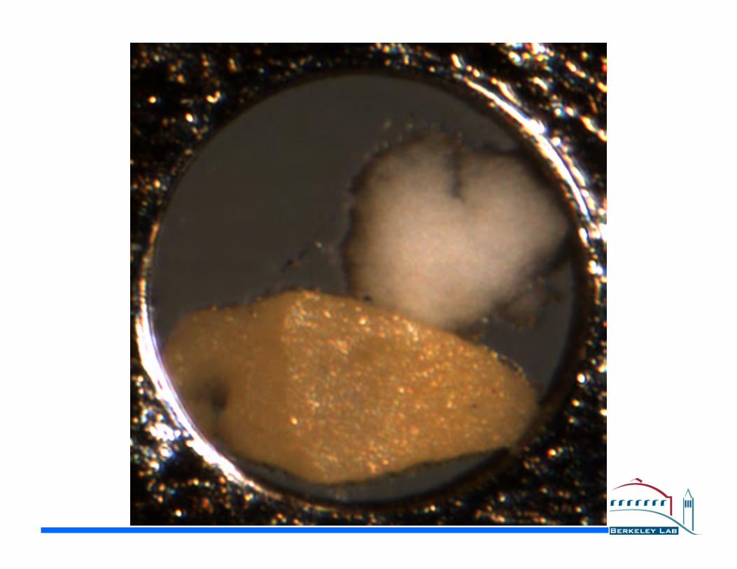
Puerto Rico soil nodule
- Grain orientation mapping
- Crystalline phases distribution
- Strain/Stress mapping
- Local plasticity/dislocationdensities
Polychromatic (white) beam microdiffraction
Monochromatic beam microdiffraction
Grain size > or ~beam size
Grain size <<beam size - Texture analysis
- Crystalline phases distribution
- Stress mapping
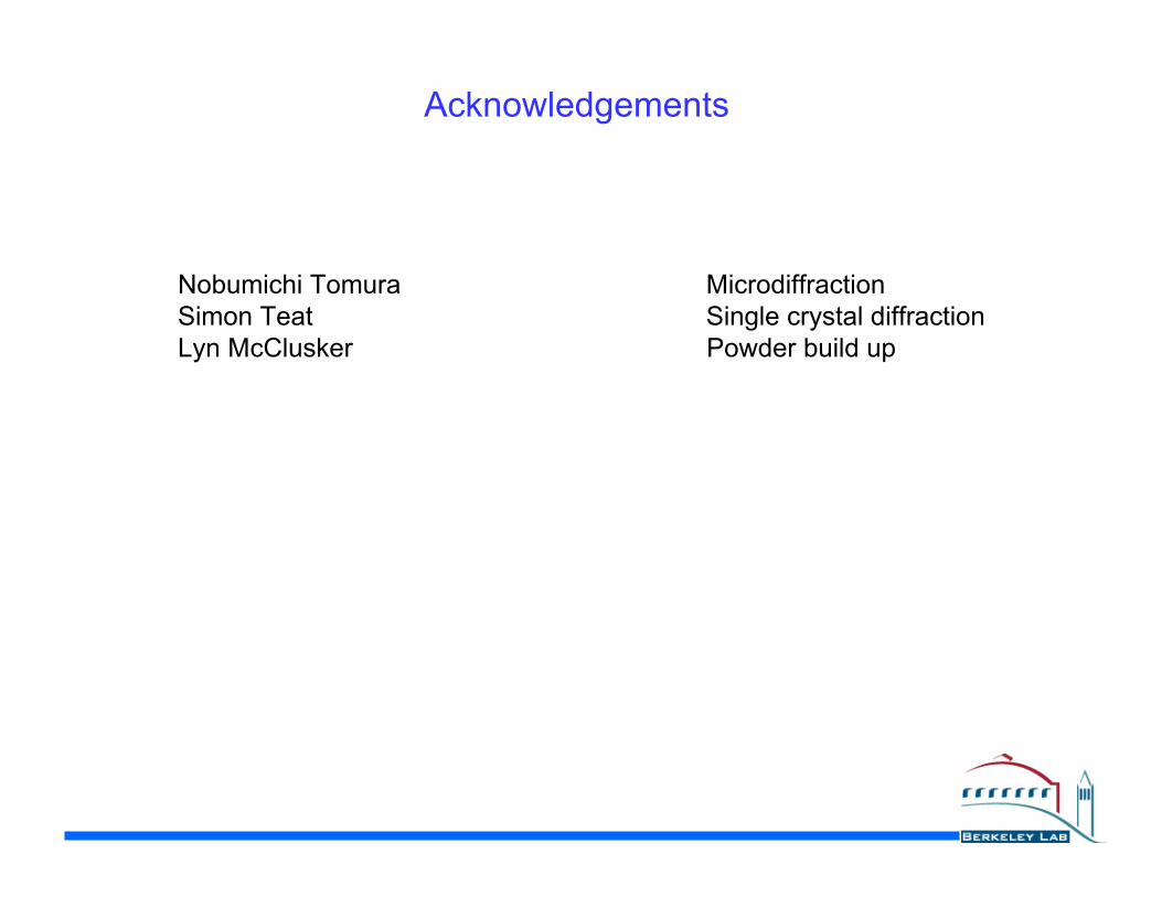
X-ray diffraction X-ray µ-diffractionAverage textureand grain size
Grain map, grainorientationrelationships,subgrains structure
Averagestrain/stress
Local deformationand residual stresswithin individualgrains
Crystalline speciesspatial distributionCrystalline
speciesidentification
Pole figure of a Cu thin film on Si
Biaxial stress-temperature curve of an Al(Cu) film on Si
Average diffractogram of a ferromanganese soilnodule
Grain map of NiTi alloy
Maximum resolved shear stress anddislocation density maps of a NiTi alloy
Mineralogical species distributionmap of a ferromanganese soil nodule
R: lithiophorite
G: goethite
B: Birnessite
100 µm
10 µm

Critical problems associated with the use of an X-raymicrobeam
Sphere of confusion No sphere of confusion
The diffracted volume is different for every sample tilt regardless ofthe position of the center of rotation of the goniometer => samplerotation must be avoided

Bend MagnetSource(250x40µm)
1:1 Toroidalmirror
1:1 imageat slits
Elevation view
Plan view
4 CrystalSi(111)Monochromator
CCDcamera
Sampleon scanningXY stage
Horizontal focusing K-B mirror Vertical focusing K-B mirror
Schematic layout of the X-ray Microdiffraction Beamline(7.3.3.) at the ALS
Beam size on sample: 0.8x0.8 µm2
Photon energy range: 5-14 keV

• Huber 6-circle diffractometer
• Bruker SMART 6000 CCD (9x9 cm2
active area)
• Si(Li) EG&G ORTEC detector
• Sample mounted on a XYZ Huber stageand a PI Piezo stage
• Heating/Cooling stage
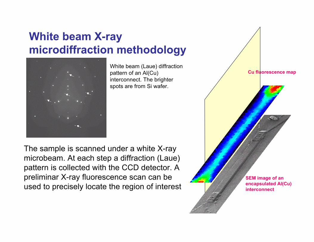
White beam X-raymicrodiffraction methodology
The sample is scanned under a white X-raymicrobeam. At each step a diffraction (Laue)pattern is collected with the CCD detector. Apreliminar X-ray fluorescence scan can beused to precisely locate the region of interest
SEM image of anencapsulated Al(Cu)interconnect
Cu fluorescence mapWhite beam (Laue) diffractionpattern of an Al(Cu)interconnect. The brighterspots are from Si wafer.

White beam X-raymicrodiffraction methodology
The indexation of the Laue patterns providethe crystal orientation matrix of the areailluminated by the X-ray microbeam. Theanalysis of the entire scan gives the grainorientation map of the sample.
Al grain orientationmap
Si spots from the wafer havebeen digitally removed. Theremaining Al spots areindexed.
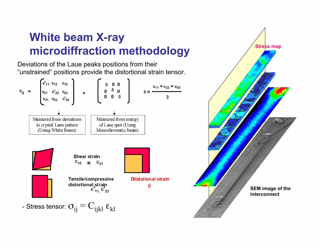
White beam X-raymicrodiffraction methodology
Deviations of the Laue peaks positions from their“unstrained” positions provide the distortional strain tensor.
SEM image of theinterconnect
Stress map
- Stress tensor: σij = Cijkl εkl
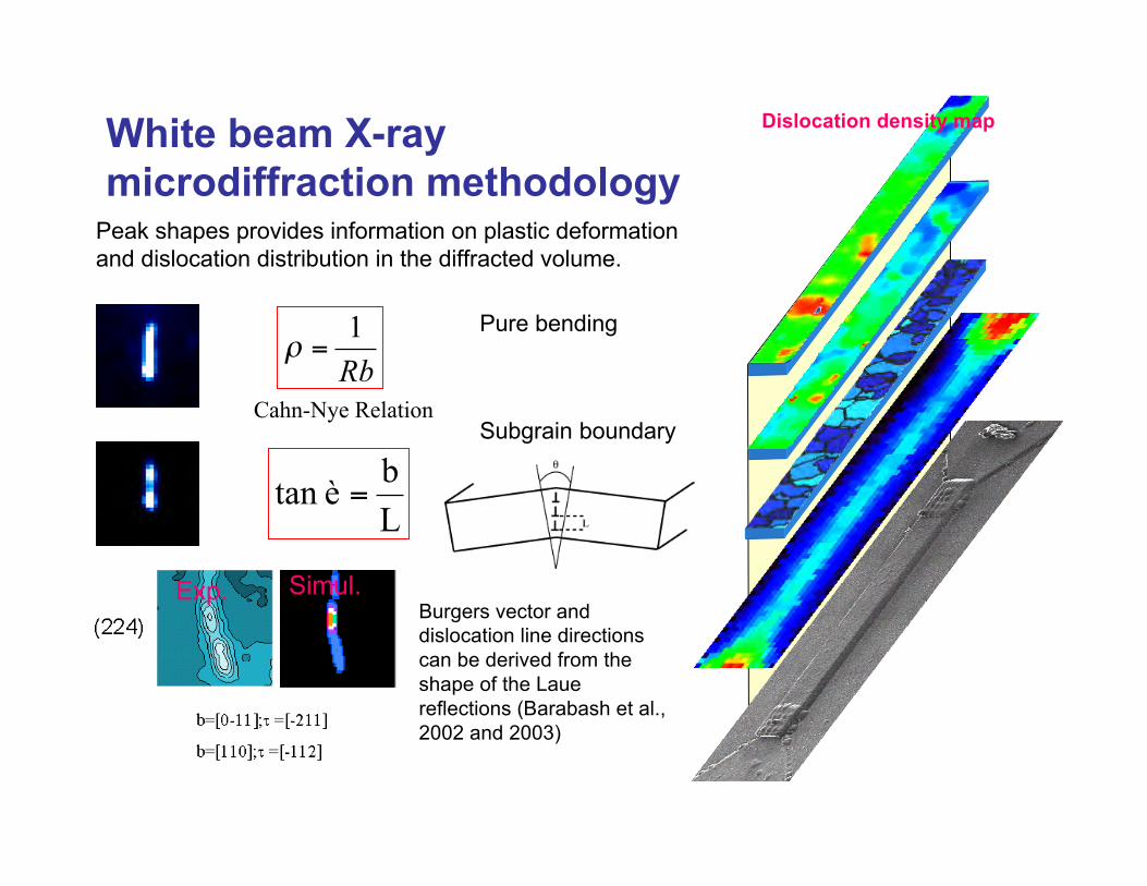
White beam X-raymicrodiffraction methodology
Peak shapes provides information on plastic deformationand dislocation distribution in the diffracted volume.
Rb
1=!
Cahn-Nye Relation
Pure bending
L
bètan =
Subgrain boundary
Exp. Simul.Burgers vector anddislocation line directionscan be derived from theshape of the Lauereflections (Barabash et al.,2002 and 2003)
Dislocation density map
Applications of X-Ray Microdiffraction
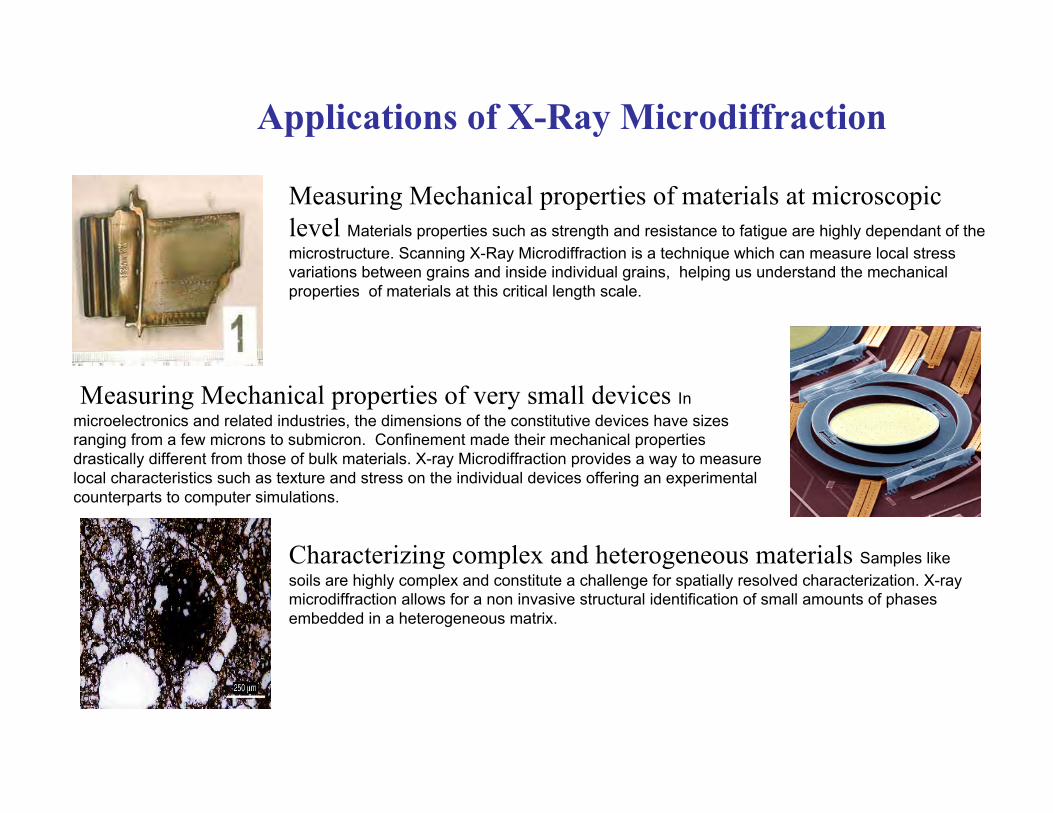
Characterizing complex and heterogeneous materials Samples likesoils are highly complex and constitute a challenge for spatially resolved characterization. X-raymicrodiffraction allows for a non invasive structural identification of small amounts of phasesembedded in a heterogeneous matrix.
Measuring Mechanical properties of materials at microscopiclevel Materials properties such as strength and resistance to fatigue are highly dependant of themicrostructure. Scanning X-Ray Microdiffraction is a technique which can measure local stressvariations between grains and inside individual grains, helping us understand the mechanicalproperties of materials at this critical length scale.
Measuring Mechanical properties of very small devices Inmicroelectronics and related industries, the dimensions of the constitutive devices have sizesranging from a few microns to submicron. Confinement made their mechanical propertiesdrastically different from those of bulk materials. X-ray Microdiffraction provides a way to measurelocal characteristics such as texture and stress on the individual devices offering an experimentalcounterparts to computer simulations.
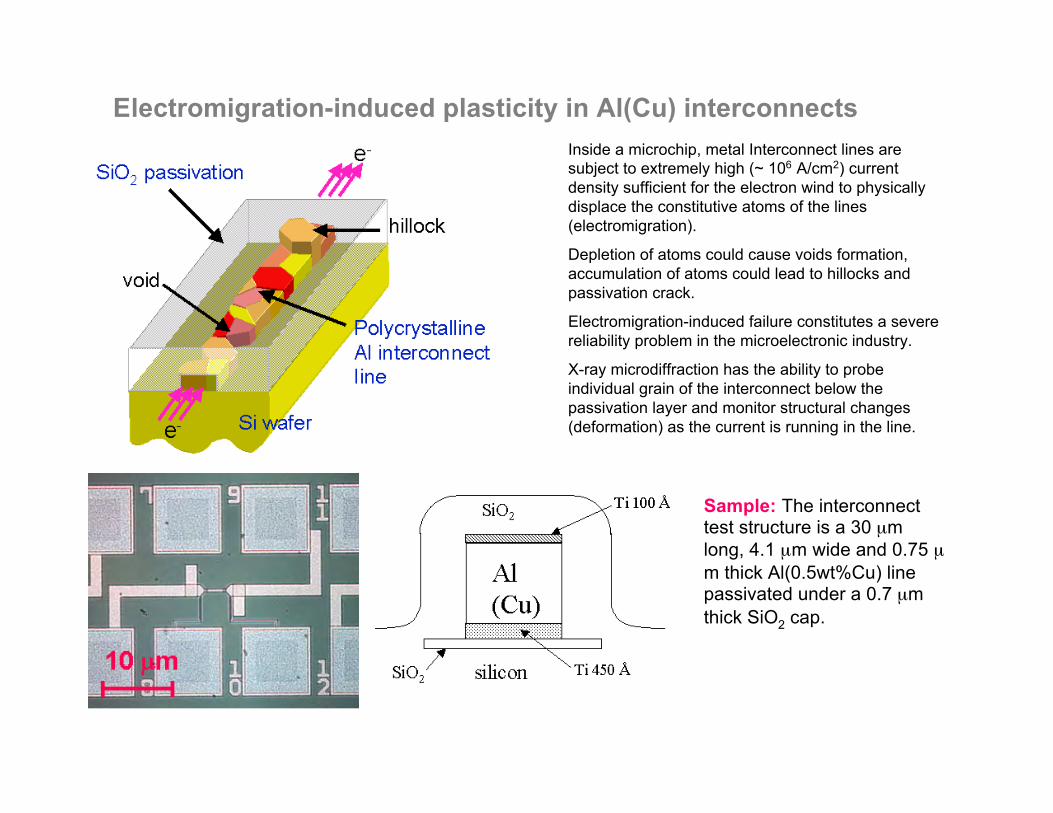
Electromigration-induced plasticity in Al(Cu) interconnectsInside a microchip, metal Interconnect lines aresubject to extremely high (~ 106 A/cm2) currentdensity sufficient for the electron wind to physicallydisplace the constitutive atoms of the lines(electromigration).
Depletion of atoms could cause voids formation,accumulation of atoms could lead to hillocks andpassivation crack.
Electromigration-induced failure constitutes a severereliability problem in the microelectronic industry.
X-ray microdiffraction has the ability to probeindividual grain of the interconnect below thepassivation layer and monitor structural changes(deformation) as the current is running in the line.
Sample: The interconnecttest structure is a 30 µmlong, 4.1 µm wide and 0.75 µm thick Al(0.5wt%Cu) linepassivated under a 0.7 µmthick SiO2 cap.
e-
e-
(220) Laue
reflection
J= 0 A/cm2
t= 0 h
J= +106 A/cm2
t= 13.55 h
J= +106 A/cm2
t= 19.45 h
J= -106 A/cm2
t= 36.15 h
J= -106 A/cm2
t= 46.30 h
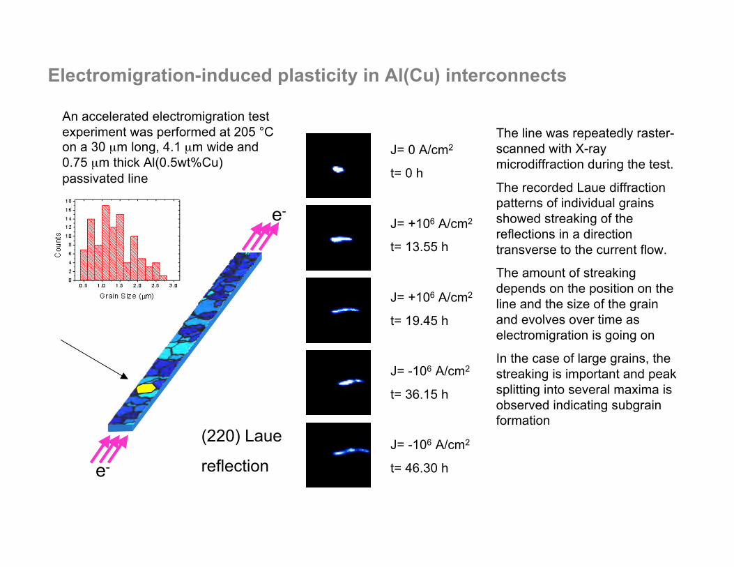
An accelerated electromigration testexperiment was performed at 205 °Con a 30 µm long, 4.1 µm wide and0.75 µm thick Al(0.5wt%Cu)passivated line
The line was repeatedly raster-scanned with X-raymicrodiffraction during the test.
The recorded Laue diffractionpatterns of individual grainsshowed streaking of thereflections in a directiontransverse to the current flow.
The amount of streakingdepends on the position on theline and the size of the grainand evolves over time aselectromigration is going on
In the case of large grains, thestreaking is important and peaksplitting into several maxima isobserved indicating subgrainformation
Electromigration-induced plasticity in Al(Cu) interconnects

e-
e-
e-
e-
t= 0 h
t= 13.55 h
t= 19.45 h
t= 36.15 h
t= 46.30 h
A small grain exhibitsless streaking of thereflections. Peak shiftingindicates grain rotationacross the line width
The rotation direction isopposite for grainssituated at opposite sideof the line width
(220) Laue
reflection
(220) Laue
reflection
Electromigration-induced plasticity in Al(Cu) interconnects

A gradient of grain deformation is establishedduring the early stage of electromigration asindicated by the position dependence of theamount of peak streaking. Grains closer tothe cathode tends to be more deformed.
A gradient of grain rotation is established aswell with grains on opposite sides of the linewidth rotating in opposite direction. Rotation ismore pronounced at the cathode end.
Electromigration-induced plasticity in Al(Cu) interconnects

Model of electromigration-inducedplastic deformation derived from the X-ray microdiffraction data
Materials travel along grain boundariesand interfaces => concentration ofvacancies at the cathode end leadingto tensile strain
Due to higher compliance of thepassivation layer, the tensile stress inthe upper half of the line is relieved bybending (subgrains formation, grainrotations).
N. Tamura et al., Appl. Phys. Lett. 80 (2002) 3724
B.C. Valek et al., Appl. Phys. Lett. 81 (2002) 4168
B.C. Valek et al., J. Appl. Phys. (2003) in press
Electromigration-induced plasticity in Al(Cu) interconnects

Electromigration-induced plasticity in Al(Cu) interconnects
Why is plastic deformation only observedtowards the cathode end?
During EM, Cu migrates from the cathode tothe anode end where Al2Cu precipitates canbe observed.
The cathode becomes Cu depleted andtherefore “softer” than the anode end andwill deform first.
Al2Cu precipitate Laue pattern
in Al(Cu) line after EM

Presentation plan
1.Why use synchrotron radiation?2.Single crystal diffraction
1.Polychromatic2.Monochromatic
3.Powder diffraction1.Monochromatic2.Polychromatic

Experimental Techniques: Beamline
Solid (small crystal or powder),liquid (in capillary or cells)
Samplerequirements
100 µmSpatial resolution1010 ph/s at sample locationFlux280 x90 µm down to 100 µm2Beam size
6-17 keV (0.73-2.07 Å)Energy range
High flux
Tunable, monochromatic
Optimized for smallmolecule crystallography.
CHARACTERISTICS
BL.11.3.1 is mounted on a regular ALS bending magnet.
Top view of BL.11.3.1 components.
Experimental Techniques: Beamline
MONOCHROMATOR

Platinum 200 CCD detector(Fairchild), four-port readout,coupled to a 20 cm diameterfiber-taper optic.
Equipped with a 3 circle, fixed-Chi (54.7°) Bruker goniometer.
Typical exposure times:- for single crystal experiments:0.5 to 5 s/frame.- for powder XRD: 120s/frame.
11.3.1 Endstation- Small Molecule Crystallography Set-up
Experimental Techniques: End-Station
The Bruker APEX2 software is usedto resolve compound structures(Single crystal XRD).
Smart or Fit 2D or Xmas are used toanalyze the powder and high pressureXRD data.
cryocooler
CCD 3-axis goniometer
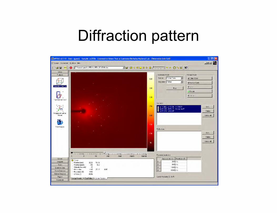
Diffraction pattern
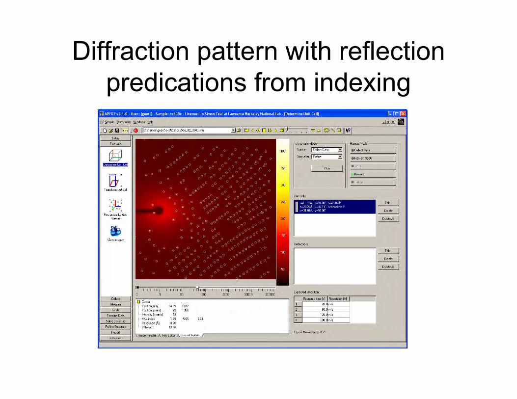
Diffraction pattern with reflectionpredications from indexing

Many of the radioactive wastes present at DOE long-term storagesites are large mixtures of metals with actinides in solution. Theselective removal of the actinides, Cs, and Sr, the predominantradioactive elements in these waste streams, would concentratethe volume of high-level waste and reduce the amounts requiringdisposal in a geological repository.
Application: Small molecule XRD
MOTIVATION
EXAMPLE 2 : FIRST SINGLE CRYSTAL XRD ANALYSISOF A Pu (IV) HYDROXYPYRIDONATE COMPLEX
A. E. V. Gorden, D.K. Shuh, B. E. F. Tiedemann, R. E. Wilson,J. Xu, K.N. Raymond, University of California and LBNL
Back to Applications
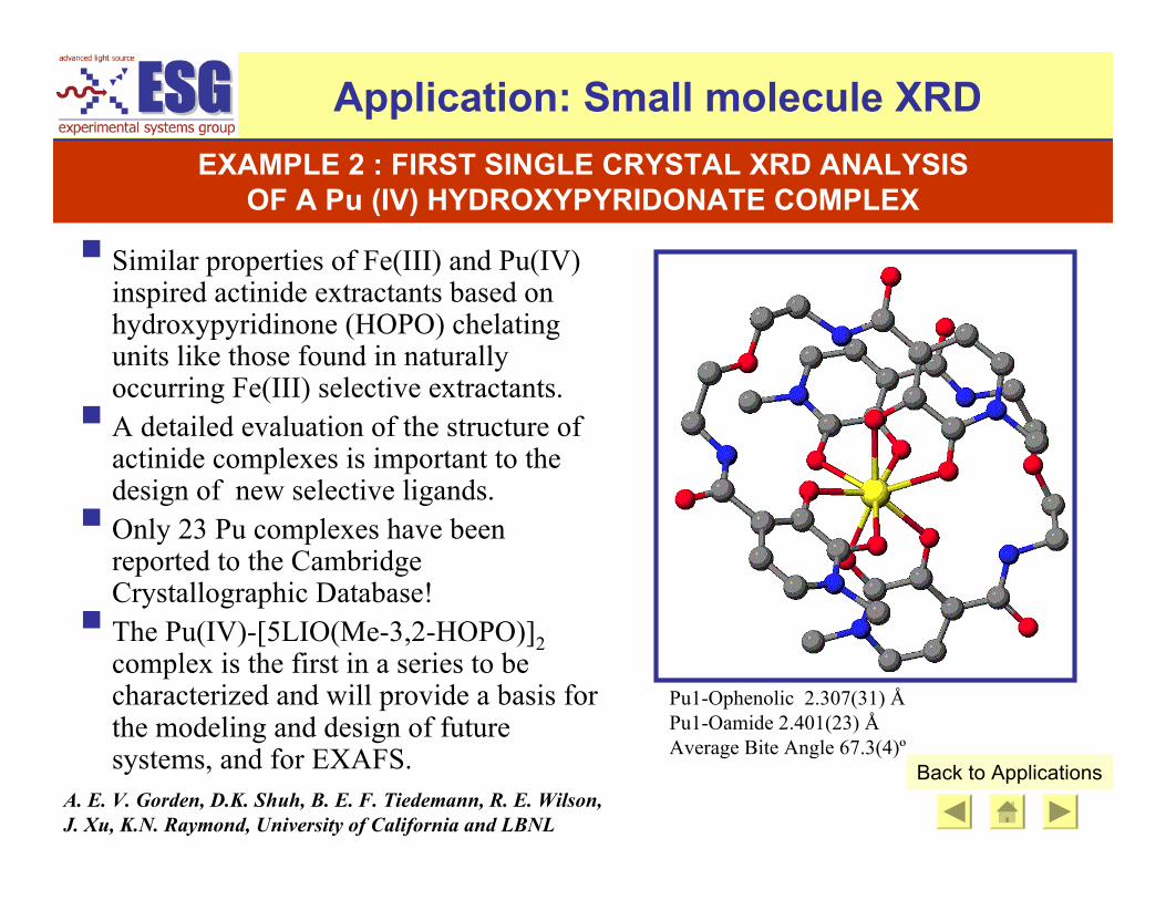
Pu1-Ophenolic 2.307(31) ÅPu1-Oamide 2.401(23) ÅAverage Bite Angle 67.3(4)º
A. E. V. Gorden, D.K. Shuh, B. E. F. Tiedemann, R. E. Wilson,J. Xu, K.N. Raymond, University of California and LBNL
Similar properties of Fe(III) and Pu(IV)inspired actinide extractants based onhydroxypyridinone (HOPO) chelatingunits like those found in naturallyoccurring Fe(III) selective extractants.
A detailed evaluation of the structure ofactinide complexes is important to thedesign of new selective ligands.
Only 23 Pu complexes have beenreported to the CambridgeCrystallographic Database!
The Pu(IV)-[5LIO(Me-3,2-HOPO)]2complex is the first in a series to becharacterized and will provide a basis forthe modeling and design of futuresystems, and for EXAFS.
Application: Small molecule XRDEXAMPLE 2 : FIRST SINGLE CRYSTAL XRD ANALYSIS
OF A Pu (IV) HYDROXYPYRIDONATE COMPLEX
Back to Applications

Pu2
Pu1
Pu1 Pu2
Application: Small molecule XRDEXAMPLE 3 : FIRST SINGLE CRYSTAL XRD ANALYSIS
OF A Pu (IV) HYDROXYPYRIDONATE COMPLEX
Pu(5LIO-Me-3,2-HOPO)2
A. E. V. Gorden, D.K. Shuh, B. E. F. Tiedemann, R. E. Wilson,J. Xu, K.N. Raymond, University of California and LBNL
Back to Applications
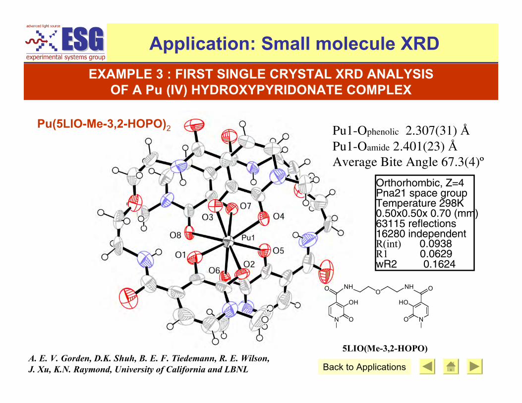
Pu1-Ophenolic 2.307(31) ÅPu1-Oamide 2.401(23) ÅAverage Bite Angle 67.3(4)º
O NHO
NH O
N N
OH
O
HO
O
5LIO(Me-3,2-HOPO)
Orthorhombic, Z=4Pna21 space groupTemperature 298K 0.50x0.50x 0.70 (mm)63115 reflections 16280 independent R(int) 0.0938R1 0.0629wR2 0.1624
Application: Small molecule XRDEXAMPLE 3 : FIRST SINGLE CRYSTAL XRD ANALYSIS
OF A Pu (IV) HYDROXYPYRIDONATE COMPLEX
Pu(5LIO-Me-3,2-HOPO)2
A. E. V. Gorden, D.K. Shuh, B. E. F. Tiedemann, R. E. Wilson,J. Xu, K.N. Raymond, University of California and LBNL Back to Applications
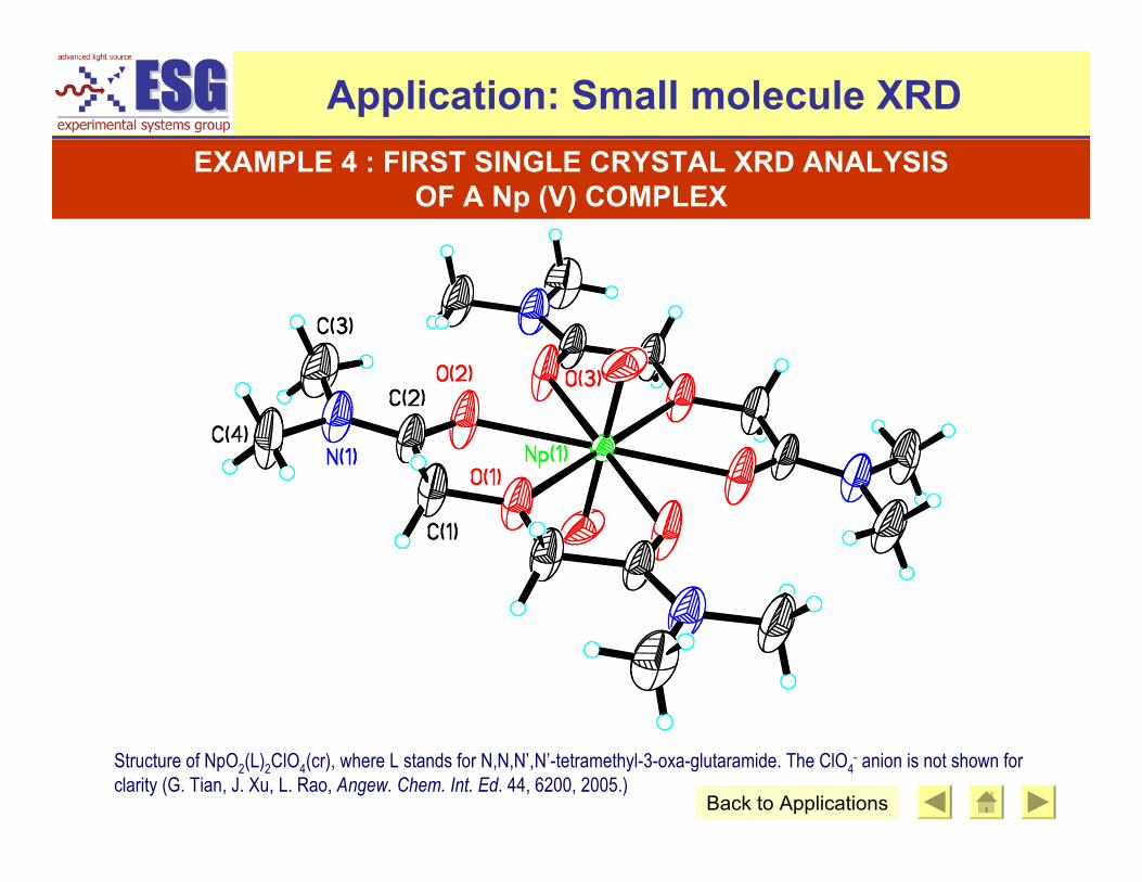
Structure of NpO2(L)2ClO4(cr), where L stands for N,N,N’,N’-tetramethyl-3-oxa-glutaramide. The ClO4- anion is not shown for
clarity (G. Tian, J. Xu, L. Rao, Angew. Chem. Int. Ed. 44, 6200, 2005.)
Application: Small molecule XRDEXAMPLE 4 : FIRST SINGLE CRYSTAL XRD ANALYSIS
OF A Np (V) COMPLEX
Back to Applications

The structure of NpO2(L)2ClO4(cr),where L stands for N,N,N’,N’-tetramethyl-3-oxa-glutaramide, was identified at theAdvanced Light Source. This is the firstneptunium complex that has beencharacterized using single-crystal x-raydiffraction with a synchrotron radiationsource. The highly symmetrical structurehelps to explain the “silence” of the opticalabsorption spectra of NpO2(L)2
+ because thef →f transition is completely forbidden. Thestructure also suggests approaches forrational design of ligands to improve thebinding ability with Np(V) and the separationof neptunium from nuclear wastes.
(G. Tian, J. Xu, L. Rao, Angew. Chem. Int.Ed. 44, 6200, 2005.)
Atomic symbols: Np (green), oxygen (red), nitrogen(blue), carbon (charcoal), hydrogen (gray, small).
Application: Small molecule XRDEXAMPLE 4 : FIRST SINGLE CRYSTAL XRD ANALYSIS
OF A Np (V) COMPLEX
Back to Applications

Presentation plan
1.Why use synchrotron radiation?2.Single crystal diffraction
1.Polychromatic2.Monochromatic
3.Powder diffraction1.Monochromatic2.Polychromatic
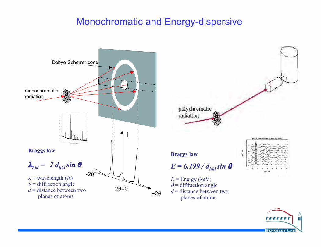
Monochromatic and Energy-dispersive
monochromaticradiation
I
-2θ
+2θ2θ=0
Debye-Scherrer cone
Braggs law
λhkl = 2 dhkl sin θ
λ = wavelength (A)θ = diffraction angled = distance between two planes of atoms
Braggs law
E = 6.199 / dhkl sin θ
E = Energy (keV)θ = diffraction angled = distance between two planes of atoms

Presentation plan
1.Why use synchrotron radiation?2.Single crystal diffraction
1.Polychromatic2.Monochromatic
3.Powder diffraction1.Polychromatic2.Monochromatic

In-situ, time-resolved studies ofHydrothermal formation of minerals
gyrolite Ca16Si24O60(OH)8.(14+x)H2Opectolite Ca2NaH(SiO3)3
S. Shaw, C.M.B. Henderson and S.M. Clark, High Pres. Res. 26(1-6) 311-324 (2001).

Walker Cell

Tungsten carbide cubes
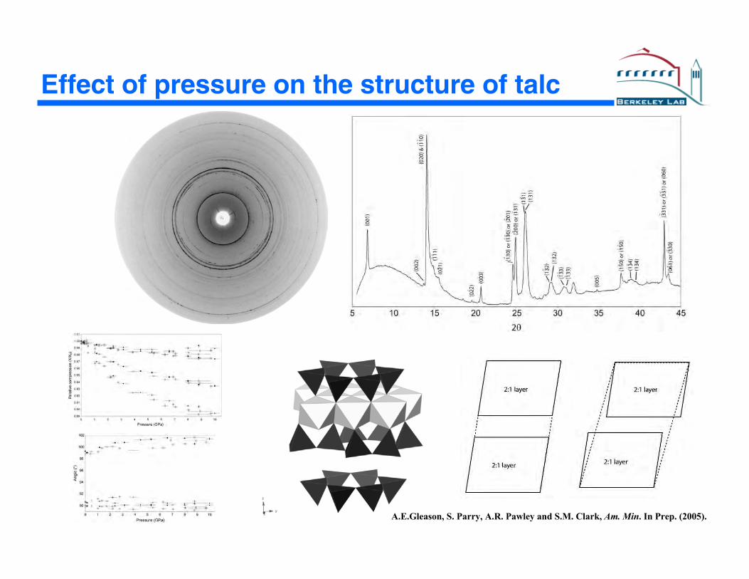
Effect of pressure on the structure of talc
A.E.Gleason, S. Parry, A.R. Pawley and S.M. Clark, Am. Min. In Prep. (2005).

Formation of 10A phase (Mg3Si4O10(OH)2.xH2O)
N.J. Chinnery, A.R. Pawley and S.M. Clark, Science 286 940-942 (1999).

Presentation plan
1.Why use synchrotron radiation?2.Single crystal diffraction
1.Polychromatic2.Monochromatic
3.Powder diffraction1.Polychromatic2.Monochromatic
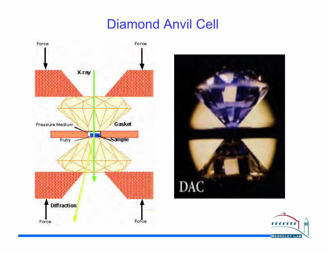
Diamond Anvil Cell

Diamond Anvil cells

Loaded cell
240 µm
Re gasket
Silicone oil pressure medium


A study of the high-low spin transition in Mg1-xFexO
A.A. Milner, S. Speziale, V.E. Lee, S.M. Clark, M.P. Pasternak, and R. Jeanloz, Spin Transition in Earth’s Mantle, PNAS, 105, 17918-17922 (2005).

Beamline 12.2.2 at the ALS
Tilt motorSuperbending MagnetSource 30 x 240 µmFWHM
M1Plane
Parabola
Phosphor coated vertical alignment aperture
Kohzu 2 Crystal Monochromator
Roll motor2nd crystal tilt
motor
Al foilphotodiode
M22:1 Toroid
Tilt motor
Ti foil beam position monitor
TV Cameraviewing beam image on Phosphor
Fast CCD shutter coated with Phosphor
ES-2 x-ray beamat sample position 10 x 10 µm2
Variable horizontal slits to adjust convergence angle
K-B mirrorfocusing pair
M. Kunz, A.A. MacDowell, W.A. Caldwell, D. Cambie, R.S. Celestre, E.E. Domning, R.M. Duarte, A.E. Gleason, J.M. Glossinger, N. Kelez, D.W. Plate, T. Yu, J.M. Zaug,H.A. Padmore, R. Jeanloz, A.P. Alivisatos, and S.M. Clark. J. Synch. Rad. 12(5) 650-658 (2005).

Review
1.Why use synchrotron radiation?2.Single crystal diffraction
1.Polychromatic2.Monochromatic
3.Powder diffraction1.Polychromatic2.Monochromatic