BACK Vertebrae & Intrinsic Back Muscles. FALSE MEMORIES Sleep deprivation and false memories.
Upload
roop-goswamiCategory
view
219download
0
8/13/2019 SwitchLevel and Memories
http://slidepdf.com/reader/full/switchlevel-and-memories 1/43
Switch Level Modeling
These Slides are just for reference, for the detailed study follow the text book.
You can Refer Verilog HDL by Samir Palnitkar (Chapter-11)

8/13/2019 SwitchLevel and Memories
http://slidepdf.com/reader/full/switchlevel-and-memories 2/43
Switch Level Modeling
MOS Switches
MOS switch keywords
nmos
Pmos

8/13/2019 SwitchLevel and Memories
http://slidepdf.com/reader/full/switchlevel-and-memories 3/43
Instantiation of NMOS and PMOS Switches
Instantiation with Instance Name
o nmos n1(out, data, control); //instantiate a nmos switcho pmos p1(out, data, control); //instantiate a pmos switch
Instantiation without Instance Nameo nmos (out, data, control); //instantiate an nmos switch; no
instance name
o pmos (out, data, control); //instantiate a pmos switch; no
instance name

8/13/2019 SwitchLevel and Memories
http://slidepdf.com/reader/full/switchlevel-and-memories 4/43
Logic Tables for NMOS and PMOS
• nmos switch conducts when its control signal is 1. If
the control signal is 0, the output assumes a highimpedance value.
• Similarly, a pmos switch conducts if the control
signal is 0.

8/13/2019 SwitchLevel and Memories
http://slidepdf.com/reader/full/switchlevel-and-memories 5/43
CMOS Switches
A cmos device can be modeled with a nmos and a pmosdevice.

8/13/2019 SwitchLevel and Memories
http://slidepdf.com/reader/full/switchlevel-and-memories 6/43
Instantiation of CMOS Switch
Instantiation with Instance Name:
cmos c1(out, data, ncontrol, pcontrol);//instantiate cmos gate.
Instantiation without Instance Name:
cmos (out, data, ncontrol, pcontrol); //no instance name given.
OR

8/13/2019 SwitchLevel and Memories
http://slidepdf.com/reader/full/switchlevel-and-memories 7/43
Power and Ground The power (Vdd, logic 1) and Ground (Vss, logic 0) sources are
needed when transistor level circuits are designed. Power and ground sources are defined with keywords supply1
and supply0.
Supply1 are equivalent to Vdd in circuits and place a logical 1 on
a net.
Supply0 are equivalent to ground or Vss and place a logical 0 on a
net.
supply1 vdd;supply0 gnd;
assign a = vdd; //Connect a to vdd
assign b = gnd; //Connect b to gnd

8/13/2019 SwitchLevel and Memories
http://slidepdf.com/reader/full/switchlevel-and-memories 8/43
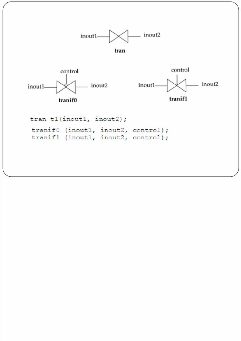
Bidirectional Switches
Switches that conduct in both directions.
Signals on either side of the device can be the driver signal.
Three keywords are used to define bidirectional switches:
8/13/2019 SwitchLevel and Memories
http://slidepdf.com/reader/full/switchlevel-and-memories 9/43

8/13/2019 SwitchLevel and Memories
http://slidepdf.com/reader/full/switchlevel-and-memories 10/43
Resistive Switches
Higher source-to-drain impedance than regular switches.
Reduce the strength of signals passing through them.
rnmos rpmos //resistive nmos and pmos switches
rcmos //resistive cmos switch

8/13/2019 SwitchLevel and Memories
http://slidepdf.com/reader/full/switchlevel-and-memories 11/43
CMOS Xor Gate

8/13/2019 SwitchLevel and Memories
http://slidepdf.com/reader/full/switchlevel-and-memories 12/43
Delay Specification on Switches
.

8/13/2019 SwitchLevel and Memories
http://slidepdf.com/reader/full/switchlevel-and-memories 13/43
Example:CMOS Nor Gate
.

8/13/2019 SwitchLevel and Memories
http://slidepdf.com/reader/full/switchlevel-and-memories 14/43
Switch Level Verilog for Nor Gate
//Define our own nor gate, my_nor
module my_nor(out, a, b);output out;
input a, b;
//internal wires
wire c;
//set up power and ground linessupply1 pwr; //pwr is connected to Vdd (power supply)
supply0 gnd ; //gnd is connected to Vss(ground)
//instantiate pmos switches
pmos (c, pwr, b);
pmos (out, c, a);
//instantiate nmos switches
nmos (out, gnd, a);
nmos (out, gnd, b);
endmodule

8/13/2019 SwitchLevel and Memories
http://slidepdf.com/reader/full/switchlevel-and-memories 15/43
2 to 1 Multiplexer using CMOS Switches .

8/13/2019 SwitchLevel and Memories
http://slidepdf.com/reader/full/switchlevel-and-memories 16/43
Switch Level Verilog Description of 2 to 1 Multiplexer
//Define a 2-to-1 multiplexer using switches
module my_mux (out, s, i0, i1);output out;
input s, i0, i1;
//internal wire
wire sbar; //complement of s//create the complement of s
// use my_nor defined previously.
my_nor nt(sbar, s, s); //equivalent to a not gate
//instantiate cmos switchescmos (out, i0, sbar, s);
cmos (out, i1, s, sbar);
endmodule

8/13/2019 SwitchLevel and Memories
http://slidepdf.com/reader/full/switchlevel-and-memories 17/43
CMOS flip-flop

8/13/2019 SwitchLevel and Memories
http://slidepdf.com/reader/full/switchlevel-and-memories 18/43

8/13/2019 SwitchLevel and Memories
http://slidepdf.com/reader/full/switchlevel-and-memories 19/43
Designs in AOI & OAI Form
And-Or-Invert Form Or-And-Invert Form
X= ((A.B)+(C.D))’ Y= ( ( a+e ).( b.f ) )’

8/13/2019 SwitchLevel and Memories
http://slidepdf.com/reader/full/switchlevel-and-memories 20/43
Practice
Design 4:1 Mux using CMOS Switches.

8/13/2019 SwitchLevel and Memories
http://slidepdf.com/reader/full/switchlevel-and-memories 21/43

8/13/2019 SwitchLevel and Memories
http://slidepdf.com/reader/full/switchlevel-and-memories 22/43
Introduction
A memory unit is a device to which binary information
is transferred for storage and from which information is
retrieved when needed for processing.
There are two types of memories that are used in digitalsystems: random-access memory(RAM) and read-only
memory(ROM).
RAM can perform both Write and Read operations.
ROM can perform Read operation.

8/13/2019 SwitchLevel and Memories
http://slidepdf.com/reader/full/switchlevel-and-memories 23/43

8/13/2019 SwitchLevel and Memories
http://slidepdf.com/reader/full/switchlevel-and-memories 24/43

8/13/2019 SwitchLevel and Memories
http://slidepdf.com/reader/full/switchlevel-and-memories 25/43
• Static RAM (SRAM) consists essentially of internal Latches
that store the binary information.
• Dynamic RAM (DRAM) stores the binary information in the
form of electric charges on capacitors provided inside the
chip by MOS transistors (require refreshing).

8/13/2019 SwitchLevel and Memories
http://slidepdf.com/reader/full/switchlevel-and-memories 26/43
Read Only Memory
Electronics and Communication Engineering26
Read Only Memories (ROM) or Programmable ReadOnly Memories (PROM) have:
N input lines,
M output lines, and
2N decoded minterms.
Fixed AND array with 2N outputs implementing all N-
literal minterms.
Programmable OR Array with M outputs lines to formup to M sum of minterm expressions.

8/13/2019 SwitchLevel and Memories
http://slidepdf.com/reader/full/switchlevel-and-memories 27/43

8/13/2019 SwitchLevel and Memories
http://slidepdf.com/reader/full/switchlevel-and-memories 28/43
Read Only Memory
Electronics and Communication Engineering28
A program for a ROM or PROM is simply a multiple-output truth table
If a 1 entry, a connection is made to the corresponding minterm
for the corresponding output
If a 0, no connection is made
Can be viewed as a memory with the inputs as addresses of
data (output values), hence ROM or PROM names!

8/13/2019 SwitchLevel and Memories
http://slidepdf.com/reader/full/switchlevel-and-memories 29/43
Representation of Array
.

8/13/2019 SwitchLevel and Memories
http://slidepdf.com/reader/full/switchlevel-and-memories 30/43
Read Only Memory Example
Electronics and Communication Engineering30
Example: A 8 X 4 ROM (N = 3 input lines, M= 4 output lines) The fixed "AND" array is a
“decoder” with 3 inputs and 8 outputs implementing min-terms.
The programmable "OR“ array uses a single line torepresent all inputs to anOR gate. An “X” in the array corresponds to attaching the
min-term to the OR
What are functions F3, F2 , F1 and F0 in terms of (A,B,C)?
D7 D6
D5 D4
D3 D2 D1 D0
A2
A1
A0
A
B
C
F0 F1 F2 F3
X XX
X
X
X
X
X
X
X

8/13/2019 SwitchLevel and Memories
http://slidepdf.com/reader/full/switchlevel-and-memories 31/43
Solution
Electronics and Communication Engineering31
F3=ABC+AB’C+A’BC’
F2=ABC+A’B’C’
F1=A’B’C+AB’C’
F0=ABC+AB’C+A’B’C

8/13/2019 SwitchLevel and Memories
http://slidepdf.com/reader/full/switchlevel-and-memories 32/43
Practice Problems:
Design Adders , Subtractor, Multiplexers etc.
E l

8/13/2019 SwitchLevel and Memories
http://slidepdf.com/reader/full/switchlevel-and-memories 33/43
Example

8/13/2019 SwitchLevel and Memories
http://slidepdf.com/reader/full/switchlevel-and-memories 34/43
6T SRAM C ll

8/13/2019 SwitchLevel and Memories
http://slidepdf.com/reader/full/switchlevel-and-memories 35/43
6T SRAM Cell

8/13/2019 SwitchLevel and Memories
http://slidepdf.com/reader/full/switchlevel-and-memories 36/43
Declaration of 2 Dimensional Array of Register Variables

8/13/2019 SwitchLevel and Memories
http://slidepdf.com/reader/full/switchlevel-and-memories 37/43

8/13/2019 SwitchLevel and Memories
http://slidepdf.com/reader/full/switchlevel-and-memories 38/43
How to initialize Memory

8/13/2019 SwitchLevel and Memories
http://slidepdf.com/reader/full/switchlevel-and-memories 39/43
Contd..

8/13/2019 SwitchLevel and Memories
http://slidepdf.com/reader/full/switchlevel-and-memories 40/43
Example

8/13/2019 SwitchLevel and Memories
http://slidepdf.com/reader/full/switchlevel-and-memories 41/43
Example: Single Port Synchronous RAM
(Read/Write)
E l Si gl P t A h

8/13/2019 SwitchLevel and Memories
http://slidepdf.com/reader/full/switchlevel-and-memories 42/43
Example: Single Port Asynchronous
RAM (Read/Write)
Verilog Code for ROM

8/13/2019 SwitchLevel and Memories
http://slidepdf.com/reader/full/switchlevel-and-memories 43/43
Verilog Code for ROM
reg [7:0] data;