Evaluation of Testability of Path Delay Faults for User-Configured Programmable Devices

Supply Voltage Noise Aware ATPG for Transition Delay Faults ∗
Nisar Ahmed and Mohammad TehranipoorDept. of Electrical & Computer Engineering
University of Connecticut
{nisar,tehrani}@engr.uconn.edu
Vinay JayaramTexas Instruments, Inc.
Dallas, TX
ABSTRACT
The sensitivity of very deep submicron designs to supply volt-age noise is increasing due to higher path delay variations andreduced noise margins with supply noise scaling. The supplynoise of delay test during at-speed launch and capture is sig-nificantly larger compared to normal circuit operation sincelarger number of transitions occur within a short time frame.Our simulations have shown that for identical switching activ-ity, a pattern with a short switching time frame window willsurge more current from the power network, thereby causinghigher IR-drop. In this paper, we propose a novel method tomeasure the average power of at-speed test patterns, referredto as switching cycle average power (SCAP). We present a casestudy of the IR-drop effects on design performance during at-speed test. A new practical framework is proposed to generatesupply noise tolerant delay test patterns. The proposed frame-work uses existing commercial ATPG tools and a wrapper isadded around them. The results demonstrate that the new pat-terns generated using our framework will significantly reducethe supply noise.
I. I NTRODUCTION
As technology shrinks and functional density and frequencyincrease, test engineers face more challenging problems to dealwith. One important issue of testing today’s nanometer, high-speed designs is the increasing number of timing-related de-fects. Transition and path delay fault models are increasinglyused to target such defects. Among these two, the transitionfault model is widely practiced in industry to test delay-induceddefects and is considered a cost-effective alternative to func-tional pattern generation [1][2]. A pattern pair is generated toinitialize the target node and launch a transition using two fastclock cycles (rated clock frequency). The at-speed launch andcapture in addition to large number of switching in the circuitcan cause excessive peak power and result in large IR-drop.
Supply noise (including IR-drop, ground bounce, and Ldi/dt)effects have become more significant in recent years and need tobe efficiently taken into consideration, as they pose design, testand reliability challenges for the chip manufacturers/foundries.This situation has grown more complicated with reducing sup-ply voltage and the limitation of further reduction of thresholdvoltage. The reduced voltage difference between the VDD andVSS pins of a standard cell will reduce the cells operating per-formance and may result in chip performance reduction if thecell is on a critical path. The IR-drop also reduces the cells
∗This work was supported in part by SRC Grant No. 2006-TJ-1455 and 2007-TJ-1587.
noise immunity and in some cases may lead to functional fail-ures [3].
There is a growing concern in EDA and semiconductor in-dustry for supply voltage noise and timing aware ATPGs. Inorder to simplify the pattern generation process, traditionallyATPGs consider zero delay gate model and target as many faultswith one pattern as possible. In other words, operating andmanufacturing conditions are ignored during ATPG. Patternsgenerated using such ATPGs may cause large number of tran-sitions in the circuit which may not occur during functional op-erating condition. As a result, a design that maynot have adelay fault may fail a delay test pattern due to excessive IR-drop related effects. This causes overkill and needs to be care-fully addressed when testing today’s large high-speed designs.Therefore, new pattern generation methods must be proposedto generate test patterns that reliably distinguish between goodand bad chips.
Supply voltage noise would be even more problematic dur-ing faster-than-at-speed test where the test patterns are appliedat higher than functional frequencies. Faster-than-at-speed testmethods have been proposed to detect small delay defects byincreasing the test frequency, i.e. reducing the positive slack ofthe path [4]. This however may result in false identification ofgood chips to be faulty due to supply noise rather than smalldelay defects [5].
A. Related Prior Work
Three major scan-based techniques have been proposed fortransition delay fault test, i.e. launch-off-shift [6], launch-off-capture [7], and enhanced scan [8]. In all three methods, apattern pair (V1, V2) is applied to target delay faults but withdifferent launch mechanisms. Pattern V2 for launch-off-shift,launch-off-capture, and enhanced scan is generated using lastshift, functional response, and arbitrary using ATPG, respec-tively. Various techniques have also been proposed to improvethe quality of at-speed test by increasing fault coverage and re-ducing pattern count [9], avoiding functionally untestable faults[10], or reducing scan enable design effort [11]. Techniqueshave been proposed to detect small delay defects either by im-proving existing ATPGs [12] or using faster-than-at-speed testapplication [4]. Note that in all cases, the launch pattern andcapture clock must be applied at either rated clock frequencyfor traditional at-speed test or higher than clock frequency forfaster-than-at-speed test. Both increase the IR-drop and maydegrade the design performance.
Authors in [13] address the issue of overkill during delay testand propose a vector-based approach for power supply noiseanalysis in test compaction. A power supply noise model is de-veloped and used during test compaction. The procedure may

������������������������������������������������������������
��������������������������������������������������������������������
������������������������������������������������������������������������
����������������������������������������������������������������
Pads
Trunks
Rails
Rings
Stripes
���������
���������
������
������
������
������
������������
������
������
���������
���������
��������
���������
���������
Fig. 1. Power/Ground Distribution Network.
become slow for large designs since all the patterns are gener-ated withoutrandom-filland the power supply noise needs to beestimated in every compaction loop. The method proposed in[14] verifies test vectors for IR-drop failures and identifies fail-ing vectors. The method estimates the average current drawnfrom power rails and compares it against a pre-defined thresh-old set by designer. A pattern generation technique is proposedin [15] by building current/voltage libraries to maximize thepower supply noise along targeted paths and cause longer prop-agation delays for the nodes along the paths. The computationcomplexity of the pattern generation procedure is high since ittargets one pattern at a time.
B. Contribution and Paper Organization
In this paper, a new method is presented to measure the aver-age power during at-speed test patterns (during fast launch andcapture of at-speed test), referred to asswitching cycle averagepower. The method considers both the length of the paths af-fected by each pattern and switching occurred during that timeframe window as opposed to calculating switching power forentire clock cycle in statistical approach. A novel pattern gen-eration procedure taking supply voltage noise into account isproposed ensuring that the supply noise will always be lowerthan defined noise threshold. The proposed procedure uses ex-isting commercial ATPG tools and adds wrapper around them.The results show that the new pattern set generated using purproposed procedure significantly reduce the IR-drop.
The rest of the paper is organized as follows. Section II ex-plains a case study with detailed statistical and dynamic IR-drop analysis for at-speed test pattern application. Section IIIpresents a new power model to measure the average switchingpower for at-speed patterns. The framework with pattern gen-eration and a technique to measure the switching cycle averagepower is discussed in Section IV. The experimental results arepresented in Section V. Finally, concluding remarks are in Sec-tion VI.
II. CASE STUDY
In this section, firstly we describe the physical design im-plementation and statistical IR-drop analysis. We, then presenta detailed dynamic IR-drop analysis for two types of patternswith different path delay distribution. Also, a new power modelis explained to measure the average power of at-speed test pat-terns which takes both the switching activity and the patternpath delay distribution into account.
A. Physical Design Implementation
For our experimentation, we had selected an ITC’99 bench-mark designb19 and the physical design implementation wasperformed using Cadence SOC Encounter place and route tool[16]. The design contains almost 219K gates, 51 IO pads, andabout 6,642 flip-flops. Scan-based test insertion was performedusing Synopsys DFT Compiler [17] with eight scan chains anda slow speed scan enable is used for launch-off-capture tran-sition fault test. During physical design, the design is timingclosed for an operating frequency of 142MHz at nominal op-erating voltage (1.8V) and temperature (25oC) conditions. Aslow scan shift speed of 10MHz was used. It is implementedin 180nmstandard cell library [18]. Note that at this point ofexperiments, no decoupling capacitances were inserted.
The power-planning for the design was performed assum-ing a net toggle probability of 20% during functional opera-tion. Figure 1 shows the power/ground distribution networkof the chip. Power rings (width = 20µm) were created us-ing higher-level routing layers (Metal5 and Metal6) and carrypower around the standard cell core area. Four power (VDD)and ground (VSS) pads each were inserted and connected to therespective rings with wires referred to as trunks. After creatingthe power rings, power and ground is routed to the standardcells using stripes and rails. The stripes (width= 10µm) werecreated using routing layer Metal4 and a distance of 100µmbe-tween adjacent stripes connecting power rings. The design wasthen placed and routed along with clock-tree synthesis and scancell ordering to minimize scan chain wirelength.
B. Statistical IR-drop Analysis
In order to determine an estimate of functional IR-drop,the design net parasitics (resistance and capacitance) were ex-tracted using Synopsys STAR-RCXT [17] extraction tool. Theaverage statistical IR-drop using vector-less approach was mea-sured for both VDD and VSS nets considering 20% net tog-gle probability during functional operation. The results showed2.8% voltage drop in VDD and a voltage bounce of 4.5% forthe VSS net, which can be considered negligible. However,such an analysis provides an underestimation of both averageand peak IR-drop even during functional operation. This is be-cause the tool considers the probability of net toggle activityover the entire cycle period (vector-less approach). However,to measure IR-drop more accurately during test a vector-basedIR-drop method must be devised to consider both the averagetime frame window for each pattern during which the entireswitching occurs and the simultaneous switching.
To measure the average IR-drop experienced by the transi-tions, it is important to estimate the average switching timeframe. The time span during which all the transitions occuris referred to as theswitching time frame window (STW). For atransition fault pattern, the maximum path length affected de-termines this time frame. Note that for different test vectors,the longest path exercised will be different. From our previ-ous experiments on the same design during transition fault testpatterns [19], we have seen anaverage switching time framewindowclose to half the clock cycle period which is mainly be-cause the ATPG tools tend to detect delay faults through shortpaths. This shows that the actual average functional power
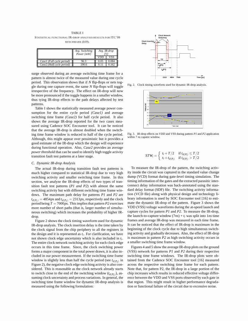
TABLE ISTATISTICAL FUNCTIONAL IR-DROP ANALYSIS RESULTS FORITC’99
BENCHMARK (b19).
Avg. Switching Avg. IR-dropPower [mW] [V]
VDD VSS
Case1 (Full cycle period) 96.3 0.05 0.084Case2 (Half cycle period) 190.6 0.11 0.162
surge observed during an average switching time frame for apattern is almost twice of the measured value during one cycleperiod. This observation shows that ifN flip-flops or nets tog-gle during one capture event, the sameN flip-flops will toggleirrespective of the frequency. The effect on IR-drop will nowbe more pronounced if the toggle happens in a smaller window,thus tying IR-drop effects to the path delays affected by testpatterns.
Table I shows the statistically measured average power con-sumption for the entire cycle period(Case1) and averageswitching time frame(Case2)for half cycle period. It alsoshows the average IR-drop reported for the two cases mea-sured using Cadence SOC Encounter tool. It can be noticedthat the average IR-drop is almost doubled when the switch-ing time frame window is reduced to half of the cycle period.Although, this might appear over pessimistic but it provides agood estimate of the IR-drop which the design will experienceduring functional operation. Also,Case2provides an averagepower thresholdthat can be used to identify high toggle activitytransition fault test patterns at a later stage.
C. Dynamic IR-drop Analysis
The actual IR-drop during transition fault test patterns ismuch higher compared to statistical IR-drop due to very highswitching activity and smaller switching time frame. In thissection, we analyze the IR-drop effects of two types of tran-sition fault test patterns (P1 and P2) with almost the sameswitching activity but with different switching time frame win-dows. The maximum path delay for patternsP1 and P2 aretd(P1) = 4854psandtd(P2) = 2313ps, respectively and the clockperiod beingT = 7000ps. This implies that patternP2exercisesmore number of short paths (that is, larger number of simulta-neous switching) which increases the probability of higher IR-drop.
Figure 2 shows the clock timing waveform used for dynamicIR-drop analysis. The clock insertion delay is the time taken bythe clock signal from the chip periphery to all the registers inthe design and it is represented asti . For clarification, we havenot shown clock edge uncertainty which is also included inti .The entire clock network switching activity for each clock edgeoccurs in this time frame. Since, the clock switching powerforms a major component in the total power drawn, it is also in-cluded in our power measurement. If the switching time framewindow is slightly less than half the cycle period (seetd(P2) inFigure 2), the negative clock edge switching activity is also con-sidered. This is reasonable as the clock network already startsto switch close to the end of the switching window (td(P2)), as-suming clock uncertainty and process variations. In general, theswitching time frame window for dynamic IR-drop analysis ismeasured using the following formulation:
Clock NetworkSwitching
Clock InsertionDelay
t (P2)d
t (P1)d
t i t i
T/2
2313 4854 7000 Time [ps]
Fig. 2. Clock timing waveform used for dynamic IR-drop analysis.
Fig. 3. IR-drop effects on VDD and VSS during patternP1andP2applicationwithin 7 nscaputre window.
STWi =
{
ti +T/2 if td(Pi) ≤ T/2ti + td(Pi) if td(Pi) > T/2
To measure the IR-drop of the pattern, the switching activ-ity inside the circuit was captured in the standard value changedump (VCD) format during gate-level timing simulation. Thetiming information of the gates and the extracted parasitic inter-connect delay information was back-annotated using the stan-dard delay format (SDF) file. The switching activity informa-tion (VCD file) along with physical design and technology li-brary information is used by SOC Encounter tool [16] to esti-mate the dynamic IR-drop of the pattern. Figure 3 shows theVDD (VSS) voltage waveforms during the at-speed launch andcapture cycles for patternP1 andP2. To measure the IR-drop,the launch-to-capture window (7ns) + ti was split into 1nstimeframes and average IR-drop was measured in each time frame.It can be noticed that the effect of IR-drop is maximum in thebeginning of the clock cycle due to high simultaneous switch-ing activity and gradually decreases. Also, the effect of IR-dropis maximum in patternP2 as high switching activity occurs ina smaller switching time frame window.
Figures 4 and 5 show the average IR-drop plots on the ground(VSS) network for patternsP1 andP2 during their respectiveswitching time frame windows. The IR-drop plots were ob-tained from the Cadence SOC Encounter tool [16] measuredacross the respective switching time frame for each pattern.Note that, for pattern P2, the IR-drop in a large portion of thechip increases which results in reduced effective voltage differ-ence between the VDD and VSS ports observed by each gate inthat region. This might result in higher performance degrada-tion or functional failure of the circuit due to excessive noise.

Fig. 4. IR-drop plot in VSS net for patternP1.
Fig. 5. IR-drop plot in VSS net for patternP2.
III. AVERAGE POWER MODEL
As we explained in the previous sections, the IR-drop de-pends on the total switching capacitance and the time framewindow during which it occurs. Since, dynamic IR-drop analy-sis for each delay test pattern is prohibitively expensive, we re-quire a model to identify test patterns which have a high prob-ability of failure due to IR-drop effects, during their applica-tion. Thecycle average power (CAP)[20] is defined as the av-erage power consumed during a single tester cycle. However, itdoes not factor in the varying time frame window of the entireswitching activity for each pattern. Therefore, a pattern withrelatively lesser switching activity but with a very short switch-ing time frame window will not be considered as a potentialpattern of IR-drop failure by the CAP power model. Therefore,we define a new term referred to asswitching cycle averagepower (SCAP)which is the average power consumed by thetest pattern during the time frame of the entire switching activ-ity (STW). CAP and SCAP are calculated by:
CAP= (ΣCi ×VDD2)/T
SCAP= (ΣCi ×VDD2)/STW
whereCi is the output gate capacitance of gateGi . Table IIshows the comparison of average power and IR-drop analysisof patternP2using the CAP and SCAP model. It can be noticedthat the power surge during the switching time frame window(SCAP) is 1.3X higher compared to the cycle average power.Also, the average IR-drop using CAP model (0.16V) reportedis within theVmin operating conditions for which the IR-dropeffect will not be of concern. In general, during sign-off, the
TABLE IIAVERAGE DYNAMIC POWER/IR-DROP ANALYSIS RESULTS OF A PATTERN
FOR CAP AND SCAPMODEL.
Avg. Switching Avg. IR-dropPower [mW] [V]
VDD VSS
CAP 163 0.120 0.161SCAP 211 0.136 0.216
TestPatterns
Design(.v)
PLIVCS STAR−RCXT
extractor
InstanceCapacitance
(DEF)Design
PowerProfile
Pattern (SPEF)Parasitics
SDF
iC
CalculatorSCAP
Fig. 6. SCAP calculator using Synopsys VCS simulator.
design is made sure to work underVmin andVmaxoperating con-ditions. However, with the SCAP model, the average IR-dropexperience by the design on VSS network (0.216V) during theswitching interval exceeds it by 34 %.
IV. PATTERN GENERATION FRAMEWORK
As explained in Section II, the switching cycle average powerprovides a more practical measure to identify patterns with veryhigh IR-drop effects bypassing the expensive dynamic IR-dropanalysis per pattern. Since, the transition fault pattern set hasvarying path delays and switching activity, the pattern genera-tion problem can be divided into two sub-problems:A) to mea-sure the switching cycle average power (SCAP) for each patternandB) to generate a new pattern set ensuring that the IR-dropwill remain under a pre-defined threshold. Both will be dis-cussed in the following sub-sections.
A. SCAP Calculator
To determine the SCAP of each pattern in the transition faultpattern set, we need the following information: 1) the gatesswitching inside the circuit, 2) output capacitance of each gateand 3) the switching time frame window. Simulation-basedtechniques can be used to capture the switching activity infor-mation in the standardvalue change dump (VCD)format. But,this technique is sufficient only to analyze a very small numberof patterns due to the extremely large size of VCD files for largedesigns.
To overcome this problem, we use programming languageinterface (PLI) routines during gate-level verilog simulation.The PLI provides a standard interface to the internal data rep-resentation of the design during simulation. Figure 6 shows theSCAP calculation flow. The capacitance per each gate instance

Fig. 7. Switching cycle average power (SCAP) measured for each transitionfault test pattern (a) VDD network and (b) VSS network.
is extracted from the RC parasitics file (Standard parasiticsexchange format (SPEF)) generated using Synopsys STAR-RCXT extraction tool. We have developed a PLI which canbe plugged into Synopsys VCS gate level simulator which actsas SCAP calculator during simulation. It reports the SCAPvalue for VDD and VSS power network for each pattern duringthe launch-to-capture window in the launch-off-capture transi-tion fault pattern set. The above procedure using PLI inter-face avoids the VCD file generation for estimation of switchingpower.
Figure 7 shows the SCAP value for VDD and VSS networkin each transition fault test pattern during the launch and cap-ture functional cycles of the launch-off-capture pattern. It canbe noticed that the initial patterns have higher switching cy-cle average power and then very gradually reduces. This isbecause the initial patterns detect most of the transition faults(exercise more paths) and the later patterns target the hard-to-detect faults.
B. Pattern Generation
In the first phase, the launch-off-capture transition fault pat-tern set (2630 patterns) were generated using Synopsys Tetra-Max [17] in the conventional manner with random fill of don’t-care bits during ATPG. Figure 8 shows the new pattern gener-ation framework which uses existing commercial ATPG tools.The generated patterns are simulated using a gate-level simu-lator and the SCAP value for each pattern is measured as ex-plained in Section IV-A. After obtaining the power pattern pro-file, it is important to set a threshold to shortlist the patterns withvery high SCAP value which relates to a lower tolerance to IR-drop effects. For this, we use the average functional switchingpower estimated using statistical-based approach as explainedin Section II-B for the SCAP threshold ans shown in Table I.A 20% toggle activity over an average switching time frame ofhalf the clock cycle period is assumed. This number is usu-ally defined by designer during power network synthesis. Theremaining patterns are calledIR-drop tolerant patterns.
No
Exit
PatternSet
FaultList
Yes
ATPG FS
Short−listedPatterns
SCAP Calculator
SCAP > ThrIf
?
CommercialATPG Tool
Fig. 8. New pattern generation framework.
Based on the functional operation SCAP threshold for boththe VDD and VSS network, the short-listed patterns are faultsimulated using the Synopsys TetraMax tool to obtain the listof extra faults detected on top of the remaining IR-drop tolerantpatterns. In the next phase of pattern generation, new patternsare generated for these set of faults withadjacent-fillor fill-X(X = 0 or 1) options. Adjacent fill causes don’t-care scan cellsto be filled with the value of the first downstream scan cell witha defined/care value (i.e. it creates runs of 0’s and 1’s in the testpattern). This option in the ATPG tool is useful to minimizepower usage as it significantly increases the correlation betweenthe initialization and launch patterns. Although, this reducedsignal switching comes at the expense of slightly higher patterncount.
V. EXPERIMENTAL RESULTS
We had generated launch-off-capture transition fault test pat-terns (2360 patterns) using conventional random fill method.As shown in Figure 7, the SCAP threshold was set to 190.6mWbased on the measured value in Table I for 20% toggle activityduring functional operation for a switching time frame windowof half the clock cycle. Based on this threshold, approximately860 patterns were short listed with high SCAP value comparedto the threshold. In the new ATPG, first the IR-drop tolerantpatterns are fault simulated. Then the short listed patterns arefault simulated and it was observed that they contribute almost10% of test coverage to the total coverage over the IR-drop tol-erant test patterns.
In the next step, we generated patterns using the don’t-carefill options built in Synopsys TetraMax for low power patterns.Note that other previously proposed low power pattern genera-tion techniques could also be used. We generated patterns withthree different fill options:Case1: fill-0, causes all don’t-carescan cells to be filled with 0’s,Case2: fill-1, causes all don’t-care scan cells to be filled with 1’s andCase3: fill-adjacent,causes don’t-care scan cells to be filled with the value of thefirst adjacent scan cell with a defined/care value.Case3ismostly useful to minimize power usage during scan shiftingby reducing signal switching at the expense of higher patterncount. However, in our experiments we are trying to reduce the

Fig. 9. Switching cycle average power (SCAP) in VDD network for the lowswitching activity test patterns generated in three cases: (a)fill-1, (b) fill-0 and(c) fill-adjacent
Fig. 10. Test coverage curves for conventional ATPG and our new supplyaware ATPG.
switching activity between the launch and capture window ofthe launch-off-capture patterns.
Figure 9 shows the switching cycle average power for theadditional patterns generated in the three different cases. Thenumber of patterns generated were 939, 957 and 900 inCase1,Case2andCase3, respectively. It can be noticed thatfill-0 pro-vided the best results with almost all the patterns below thethreshold. Figure 10 shows the test coverage curve for thetwo pattern generation methods. It can be seen that our tech-nique generates approximately 957 patterns (fill-0) for the 10%coverage of the short-listed patterns, which is a very slight in-crease in the number of patterns (approximately 97 additionalpatterns). Therefore, the increase in test time is not very signifi-cant with almost all of the patterns in the new pattern set withinthe threshold limit.
VI. CONCLUSION
We have presented a detailed analysis of at-speed tech-niques which illustrates that modeling IR-drop requires boththe switching activity and the switching time frame window,
i.e. the path delay distribution of the pattern. The switching cy-cle average power (SCAP) proposed captures both of these ef-fects and provides a good model to identify patterns with higherIR-drop effects. We have proposed a new framework for gener-ating transition fault test patterns which are tolerant to IR-dropeffects. This avoids the false classification of good die as faulty,where the fault effects are caused due to IR drop related reasons.The experimental results show approximately 4 % increase innumber of test patterns over the conventionally generated tran-sition fault pattern set.
ACKNOWLEDGEMENTS
We thank Ken Butler and Jayashree Saxena of Texas Instru-ments for useful discussions during the course of this work andfeedback on the initial draft of the paper.
REFERENCES
[1] J. Saxena, K. M. Butler, J. Gatt, R. Raghuraman, S. P. Kumar, S. Basu,D. J. Campbell, J. Berech, “Scan-Based Transition Fault Testing - Im-plementation and Low Cost Test Challenges,” in Proc.International TestConference (ITC’02), pp. 1120 - 1129, Oct. 2002.
[2] X. Lin, R. Press, J. Rajski, P. Reuter, T. Rinderknecht, B. Swanson and N.Tamarapalli, “High-Frequency, At-Speed Scan Testing,”IEEE Design &Test of Computers, pp. 17-25, Sep-Oct 2003.
[3] M. Nourani, M. tehranipoor and N. Ahmed, “Pattern Generation and Es-timation for Power Supply Noise Analysis,” in proc.VLSI Test Symo.(VTS’05), pp. 439-444, 2005.
[4] B. Kruseman, A. K. Majhi, G. Gronthoud and S. Eichenberger, “Onhazard-free patterns for fine-delay fault testing,” in Proc.Int. Test Conf.(ITC’04), pp. 213-222, 2004.
[5] N. Ahmed, M. Tehranipoor and V. Jayaram, “A Novel Framework forFaster-than-at-Speed Delay Test Considering IR-Drop Effects,” to appearin Int. Conf. on Computer-Aided Design (ICCAD’06), 2006.
[6] J. Savir, “Skewed-Load Transition Test: Part I, Calculus,” in Proc.Int.Test Conf. (ITC’92), pp. 705-713, 1992.
[7] J. Savir and S. Patil, “On Broad-Side Delay Test,” in Proc.VLSI TestSymp. (VTS’94), pp. 284-290, 1994.
[8] B. Dervisoglu and G. Stong, “Design for Testability: Using ScanpathTechniques for Path-Delay Test and Measurement,” in Proc.Int. TestConf. (ITC’91), pp. 365-374, 1991.
[9] N. Ahmed and M. Tehranipoor, “Improving Transition Delay Fault Cov-erage Using Hybrid Scan-Based Technique,” in Proc.Int. Symp. on Defectand Fault Tolerance in VLSI Systems (DFT’05), pp. 187-195 , 2005.
[10] X. Liu and M. Hsiao, “Constrained ATPG for Broadside Transition Test-ing,” in Proc. IEEE Int. Symp. on Defect and Fault Tolerance in VLSISystems (DFT’03), pp. 175-182, 2003.
[11] N. Ahmed, C.P. Ravikumar, M. Tehranipoor and J. Plusquellic, “At-SpeedTransition Fault Testing With Low Speed Scan Enable,” in proc.IEEEVLSI Test Symposium (VTS’05), pp. 42-47, 2005
[12] P. Gupta and M. S. Hsiao, “ALAPTF: A new transition fault model andthe ATPG algorithm,” in Proc.Int. Test Conf. (ITC’04), pp. 1053-1060,2004.
[13] J. Wang, Z. Yue, X. Lu, W. Qiu, W. Shi, D. M. H. Walker, “A Vector-based Approach for Power Supply Noise Analysis in Test Compaction,”in Proc.Int. Test Conf. (ITC’05), 2005.
[14] A. Kokrady and C.P. Ravikumar, “Static Verification of Test Vectors forIR-drop Failure,” in Proc.Int. Conf. on Computer-Aided Design (IC-CAD’03), pp. 760-764, 2003.
[15] A. Krstic, Y. Jiang and K. Cheng, “Pattern Generation for Delay Testingand Dynamic Timing Analysis Considering Power-Supply Noise Effects,”in IEEE Transactions on CAD, vol. 20, No. 3, pp. 416-425 March 2001.
[16] Cadence Inc., “User Manuals for Cadence Encounter Tool set Version2004.10,” Cadence, Inc., 2004.
[17] Synopsys Inc., “User Manuals for SYNOPSYS Toolset Version 2005.09,”Synopsys, Inc., 2005.
[18] http://crete.cadence.com, 0.18µm standard cell GSCLib library version2.0, Cadence, Inc., 2005.
[19] N. Ahmed, M. Tehranipoor and V. Jayaram, “Timing-Based Delay Testfor Screening Small Delay Defects,” in Proc.Design Automation Confer-ence (DAC’06), pp. 320-325 , 2006
[20] J. Saxena, K. M. Butler, V. Jayaram, S. Kundu, N. V. Arvind, P. Sreep-rakash and M. Hachinger, “A Case Study of IR-Drop in Structured At-Speed Testing,” in Proc.International Test Conference (ITC’03), pp. 1098- 1104, Oct. 2003.