sue-m-1331 REVIEW OF SUB-NANOSECOND T&E … · A review of time-interval measurements in the sub-...
17
REVIEW OF SUB-NANOSECOND T&E-INTERVAL MEASUREMENTS* Dan I. Porat Stanford Linear Accelerator Center Stanford University, Stanford, California 94305 sue-m-1331 (1) October 1973 ABSTRACT A review of time-interval measurements in the sub- nanosecond regime is presented and the various methods are compared as to their precision, stability, resolution, and other essential parameters. Calibration methods, stabili- zation, and correction for time walk are also discussed. 1. INTRODUCTION In many physics experiments a need arises to measure short time intervals with good resolution and accuracy. Such experiments are in the area of mean lifetime measure- ments of excited nuclear states, angular correlation func- tions, time-of-flight measurements, particle identification, and any nuclear physics experiments in which time informa- tion is either essential or auxiliary in reconstructing an event. Particles interacting with matter generate electrical pulses which have to be measured with the best accuracy, stability and resolution consistent with the experimental requirements. The time intervals to be discussed in this paper span six decades being in the range of lo-I2 to 10-6 s although some techniques can easily be adapted to extend the upper limit. Accuracies and resolutions are of the order of 1 percent in most circuits to be discussed; some techniques, however, are capable of higher accuracies and resolutions. At present the principal limitation in measurement accuracies lies in the transducers such as photomultipliers or semiconductor detectors. The electrical signals gener- ated by these transducers exhibit transition times that are much longer than the accuracies required in many time- interval measurements. The detector is commonly followed by a discriminator-shaper circuit which, ideally, delivers a pulse of standard amplitude, duration, or both once its threshold has been exceeded by the incoming signal. The time definition of the output of such a discriminator-shaper circuit is degraded due to the finite risetime of the incoming signal. and the large dynamic range typical in particle detecij:ln. Several schemes have been developed to mini- mize the timing errors from the above sources and these were tliscussed in this issue in A. Barna’s paper on “Nano- second Trigger Circuits” and F. Kirsten’s paper on “Nano- second Coincidence Measurements. I’ We can therefore mininliLc! in this paper all discussion pertaining to lack of time rc>solution resulting from the detector properties and concentrate the treatment on the types of circuits available for short time-interval measurements, their relative merits and linlitations and their typical applications. WC shall make a distinction between a systems resolu- tion and the intrinsic resolution of a measurement. The former takes into consideration the contribution to the reso- lution from all components of the system while the latter is restricted to the resolution of the time-interval measuring machine only. In the following we describe the principal methods of time-interval measurement: (a) Time-to-digital converters, TDC’s, using counter methods, (1,) vernier techniques, (c) pulse overlap techniques, (d) circuits utilizing the start-stop principle, and (e) picosecond measurements utilizing the RF structure uf accelerated particles. *Work supported by the U. S. Atomic Energy Commission. Time scale and time delay calibration are discussed in Section 7. Since many experiments involve accumulation of data over extended period we have included a section (Section 8) on stabilization of time-interval measurements. Finally, in Section 9 we discuss applications and some practical considerations. 2. TIME-TO-DIGITAL CONVERTERS, TDC’s, USING COUNTER METHODS The TDC principle utilizes a gated time-marker gener- ator of a well-defined and stable period T. The generator is gated on by the start pulse and gated off by the stop pulse. A counter records the number n of time markers wjthin the start-stop time interval as shown in Figure 1. The dynamic range of the instrument is large and depends only on the bit capacity of the counter; its integral linearity is ver)’ good. The accuracy is defined by the stability of the gener:LLor frequency. The time resolution is T and with modern counters having a 500 MHz toggling rate T is thus 2 ns. The resolution of such a TDC may be improved by use of two 500 MHz oscillators that are synchronized to start on oppo- site phases of the period as shown in Figure 2. A resolution of 1 ns is thus obtained at the expense of using an additional counter. Further improvements are possible through use of several phase controlled oscillators to obtain a sub&vision of the clock period. Thus De Lotto et al. using a 1.25 GHz oscillator achieved a 50 ps resolutioyza=O. 25% by sub- dividing the period into 16 intervals (Lo 64). These compli- cations in circuitry are justified when a large dynamic range is required. They have been successfully employed in TDCQ having a resolution of 1 ns in a range of 217 ns (Me 66). When the clock frequency is about 100 MHz one can utilize an interpolation circuit to obtain resolutions of about 1 ns. A simplified block diagram of a representative cir- cuit, is shown in Figure 3. Assume that the clock frequency is 125 MHz, i.e., a period of 8 ns. A delay line with taps at 1 ns intervals is inserted in the signal path; each delay tap is connected to a coincidence circuit having 1 ns reso- lution. Initially the counter starts accumulating counts after the oscillator has been gated by a start pulse. A stop puise is simultaneously applied to (a) the gated oscillator to stop further oscillations and to @) the second inputs of all coincidence units. The interpolated time interval thus obtained is e:lcoded and presented as the least significant three bits together with the counter bits. Interpolation schemes of this type suffer from differ- ential non-linearities which have a periodicity of the oscil- lator period. Such non-linearities may be minimized using an additional interpolation unit in the stop channel that is incremented modulo n by one unit delay at each measure- ment, where n is the number of subdivisions. The added delay value at each measurement is digitally subtracted from the number formed by the counter and interpolator outputs to yield the correct result. This statistical equali- zation of the interpolated time reduces the differential non- linearities to negligible values. 3. VERNIER PRINCIPLE The vernier principle is illustrated in Figure 4; two clocks of slightly different periods are employed and the (PrinTed in IEEE Trarx. on BL?cl. SC;. Vol. WT-2;, IJO. ;, p. y&j1 (1973))
Transcript of sue-m-1331 REVIEW OF SUB-NANOSECOND T&E … · A review of time-interval measurements in the sub-...

REVIEW OF SUB-NANOSECOND T&E-INTERVAL MEASUREMENTS*
Dan I. Porat Stanford Linear Accelerator Center
Stanford University, Stanford, California 94305
sue-m-1331 (1) October 1973
ABSTRACT
A review of time-interval measurements in the sub- nanosecond regime is presented and the various methods are compared as to their precision, stability, resolution, and other essential parameters. Calibration methods, stabili- zation, and correction for time walk are also discussed.
1. INTRODUCTION
In many physics experiments a need arises to measure short time intervals with good resolution and accuracy. Such experiments are in the area of mean lifetime measure- ments of excited nuclear states, angular correlation func- tions, time-of-flight measurements, particle identification, and any nuclear physics experiments in which time informa- tion is either essential or auxiliary in reconstructing an event. Particles interacting with matter generate electrical pulses which have to be measured with the best accuracy, stability and resolution consistent with the experimental requirements. The time intervals to be discussed in this paper span six decades being in the range of lo-I2 to 10-6 s although some techniques can easily be adapted to extend the upper limit. Accuracies and resolutions are of the order of 1 percent in most circuits to be discussed; some techniques, however, are capable of higher accuracies and resolutions.
At present the principal limitation in measurement accuracies lies in the transducers such as photomultipliers or semiconductor detectors. The electrical signals gener- ated by these transducers exhibit transition times that are much longer than the accuracies required in many time- interval measurements. The detector is commonly followed by a discriminator-shaper circuit which, ideally, delivers a pulse of standard amplitude, duration, or both once its threshold has been exceeded by the incoming signal. The time definition of the output of such a discriminator-shaper circuit is degraded due to the finite risetime of the incoming signal. and the large dynamic range typical in particle detecij:ln. Several schemes have been developed to mini- mize the timing errors from the above sources and these were tliscussed in this issue in A. Barna’s paper on “Nano- second Trigger Circuits” and F. Kirsten’s paper on “Nano- second Coincidence Measurements. I’ We can therefore mininliLc! in this paper all discussion pertaining to lack of time rc>solution resulting from the detector properties and concentrate the treatment on the types of circuits available for short time-interval measurements, their relative merits and linlitations and their typical applications.
WC shall make a distinction between a systems resolu- tion and the intrinsic resolution of a measurement. The former takes into consideration the contribution to the reso- lution from all components of the system while the latter is restricted to the resolution of the time-interval measuring machine only.
In the following we describe the principal methods of time-interval measurement:
(a) Time-to-digital converters, TDC’s, using counter methods,
(1,) vernier techniques, (c) pulse overlap techniques, (d) circuits utilizing the start-stop principle, and (e) picosecond measurements utilizing the RF
structure uf accelerated particles.
*Work supported by the U. S. Atomic Energy Commission.
Time scale and time delay calibration are discussed in Section 7. Since many experiments involve accumulation of data over extended period we have included a section (Section 8) on stabilization of time-interval measurements. Finally, in Section 9 we discuss applications and some practical considerations.
2. TIME-TO-DIGITAL CONVERTERS, TDC’s, USING COUNTER METHODS
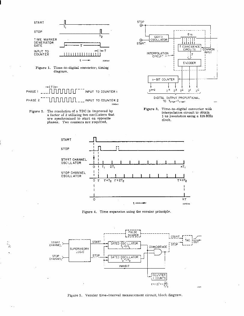
The TDC principle utilizes a gated time-marker gener- ator of a well-defined and stable period T. The generator is gated on by the start pulse and gated off by the stop pulse. A counter records the number n of time markers wjthin the start-stop time interval as shown in Figure 1. The dynamic range of the instrument is large and depends only on the bit capacity of the counter; its integral linearity is ver)’ good. The accuracy is defined by the stability of the gener:LLor frequency. The time resolution is T and with modern counters having a 500 MHz toggling rate T is thus 2 ns. The resolution of such a TDC may be improved by use of two 500 MHz oscillators that are synchronized to start on oppo- site phases of the period as shown in Figure 2. A resolution of 1 ns is thus obtained at the expense of using an additional counter.
Further improvements are possible through use of several phase controlled oscillators to obtain a sub&vision of the clock period. Thus De Lotto et al. using a 1.25 GHz oscillator achieved a 50 ps resolutioyza=O. 25% by sub- dividing the period into 16 intervals (Lo 64). These compli- cations in circuitry are justified when a large dynamic range is required. They have been successfully employed in TDCQ having a resolution of 1 ns in a range of 217 ns (Me 66).
When the clock frequency is about 100 MHz one can utilize an interpolation circuit to obtain resolutions of about 1 ns. A simplified block diagram of a representative cir- cuit, is shown in Figure 3. Assume that the clock frequency is 125 MHz, i.e., a period of 8 ns. A delay line with taps at 1 ns intervals is inserted in the signal path; each delay tap is connected to a coincidence circuit having 1 ns reso- lution. Initially the counter starts accumulating counts after the oscillator has been gated by a start pulse. A stop puise is simultaneously applied to (a) the gated oscillator to stop further oscillations and to @) the second inputs of all coincidence units. The interpolated time interval thus obtained is e:lcoded and presented as the least significant three bits together with the counter bits.
Interpolation schemes of this type suffer from differ- ential non-linearities which have a periodicity of the oscil- lator period. Such non-linearities may be minimized using an additional interpolation unit in the stop channel that is incremented modulo n by one unit delay at each measure- ment, where n is the number of subdivisions. The added delay value at each measurement is digitally subtracted from the number formed by the counter and interpolator outputs to yield the correct result. This statistical equali- zation of the interpolated time reduces the differential non- linearities to negligible values.
3. VERNIER PRINCIPLE
The vernier principle is illustrated in Figure 4; two clocks of slightly different periods are employed and the
(PrinTed in IEEE Trarx. on BL?cl. SC;. Vol. WT-2;, IJO. ;, p. y&j1 (1973))

time interval T to be measured is expanded by a factor k, under measurement,
=1 T1 f2 f2 k=T,-T,=x=--- f2-fI Af (1)
T = nlT1 - n2T2 = (“I-n2) TI + n2 AT
Note that for r < Tl, n1=n2 and Eq. (4) reduces to Eq. (2).
where
fI = + is the lower oscillation frequency 1
f2 = $- is the higher oscillation frequency 2
Equation (1) can be easily derived from Figure 4 and is valid for T < TJ . Accuracy and resolution of the instrument can be very high if (a) fI, f are stable and (b) Af can be made arbitrarilv small. T E e first condition is easilv achievable within the accuracies normally required for short time-interval measurements, However, operation of two frequency sources having a small Af is possible only with careful shielding, otherwise the oscillators lock into a con- stant relative phase and have identical periods. A Af of 1% is usually employed but this figure could be improved. A supervisory circuit is required to prevent inputs to the vernier time analyzer during conversion and for input pulses where r > TI.
The block diagram of a typical vernier time interval measurement circuit is shown in Figure 5. The oscillators are gated on by the start and stop pulses, respectively. Since T2 < Tl the number of accumulated periods in the stop channel gradually catches up with the start channel as shown in Figure 4; when both oscillators are in phase n1=n2 =n and the coincidence circuit delivers an output which gates off both frequency sources at a time k T
kr =nTl=r +nT2
thus
Af T = n(T2-T1) = nAT = n T2
As shown in Figure 5 the measurement employing a vernier type device may be carried out either by measuring the expanded time, k7, using a relatively slow, time-to- \ amplitude converter, TAC (see dashed lines) or by count- i ing the periods n until the phases of the two channels are in
. coincidence (see full lines). The latter method has the advan’:lge that the output is derived in digital form and is therefore compatible with modern data acquisition systems. In either case 7 is quantized to time intervals of AT duration.
The vernier method may also be used to measure in- tervals r > TI, in which case nIfn2 and the time expansion, k, derived from the time diagram of Figure 4 is
(3)
As in the case of T <Tl two gated oscillators of periods TI and T, (TI>T2) are required having slightly different periocrs.. The start and stop pulses determine the initial relative phases of the oscillators. If the later pulse (stop) is appIicd to the osciIlator having the shorter period the two oscillators will be in phase coincidence after some time during \\rhich the start oscillator has completed nl periods while !he stop oscillator has completed n2 periods. TWO countt,l‘s are now required to establish the time interval r
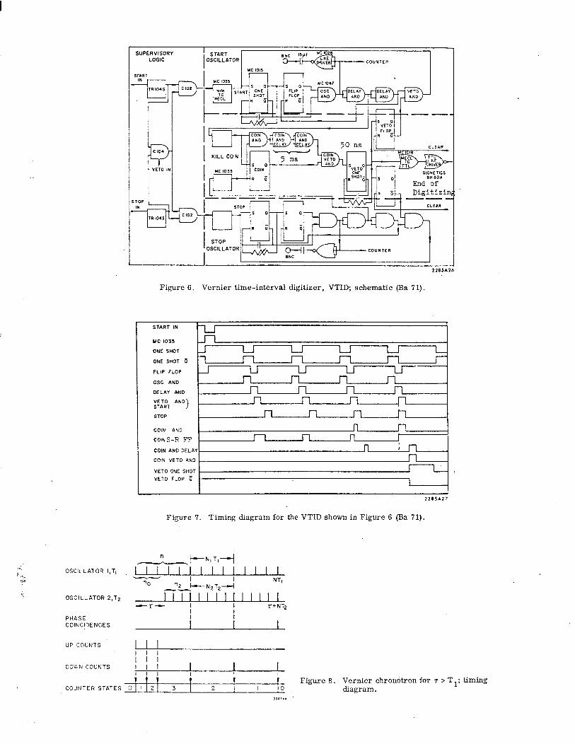
A vernier time-interval digitizer (VTID) utilizing two counters and hence capable of measuring r < TI as well as T >Tl is described by Barton and King (Ba 71). The diagram of the instrument that was constructed using MECL II logic is shown in Figure 6 and the timing wave forms in Figure 7. Referring to Figure 6 the circuit may be divided into (a) the supervisory logic (made up of EG&G logic modules) which allows the circuit to operate when the time interval is on scale and when necessary conditions obtain, e.g., computer ready to accept data, and (b) the VTID circuitry. The latter consists of start and stop circulating loops and an inhibit circuit. An initial start pulse sets the upper loop into oscil- lation with a period determined by gate delays and by the RC time constant of the flip-flop utilized as a one-shot. This loop establishes TI; the number of periods is recordctl by a counter. The stop channel is constructed in an identical manner. The inhibit, or I’ kill coincidence” circuit accepts pulses from both, the start and the stop channel. The COIN FF changes states with each application of a stirt or stop pulse. However, the VETO one-shot is not trigsc-red until the stop pulse has completely overlapped or is ahead of the start pulse, as shown in Figure 7. The duratiun of the veto pulses is longer than the period of either chnnnel and this pulse is utilized to inhibit the circulating 1001~s thus stopping the oscillators. The contents of two counters that record the number of recirculations are used to establish the time interval under measurement in accordance with Eq. (4).
This VTID has a variable resolution with a minimum of 16 ps/channel, and an integral linearity with a statistical confidence level of 27% to Sl%, depending on channel width. Differential linearity was established to be within the sm- tistical fluctuations of the measurement at 3500 counts/ channel (5 1.7%).
The intrinsic time resolution of this circuit (and of all VTID circuits), neglecting the problems associated with in- put pulse timing, may be expressed as $.,,,1= o+ ph. a! is the time jitter contributed by the input (start and stop) circuits and by the resolution of the inhibit circuit. The second term P.&n, arises, from the phase noise in each oscillator; therefore, the uncertainty of the occurrence of the nth pulse (at coincidence) should be proportional to .J!n. This has been verified experimentally for the circuit of Figure 6 yielding Q= 9.4 ps and p = 13.7 ps. In practice the limitation on resolution are predominantly determined by the detector rather than the measuring circuitry. It has been shown (Ba 71) that for an intrinsic resolution that is half the detector resolution the total system’s resolution is degraded by less than 12% due to circuitry.
The dynamic range of vernier measurements described earlier in this section cannot exceed the time expansion factor k. However, when 7 > T the time expansion factor may be increased considerably t t ough accumulation of several coincidences between the 2 clock phases. As shown in Figure 8 an up-down counter increments during the in- terval r to record an integer number of T periods. At t=r the stop channel oscillator is activate d . havmg a period T2<TI. Phase coincidences between the two oscillators are utilized to decrement the same counter. An output is obtained at time 1~~ when the counter has reached 0 state againas shoal in the last line of the figure.
Denoting by no the number of integer up counts such that nOTI < r and N the number of phase coincidences between fi two oscll ators, .E we deduce from Figure 8 the
-2-
total number of counts, N,
N=n1+NlNc=n2+N2Nc , (5)
where the symbols of Eq. (5) are defined in the figure. Further, since no = nI-n2 and NlT l = N2T2 it follows that
no = Nc(N2-N1) = N c ’ since N2-N1=l.
4. TIME OVERLAP PRINCIPLE
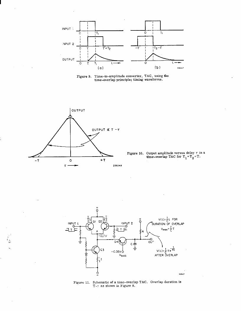
This time-to-amplitude converter evolved from coinci- dence circuits; its output amplitude is proportional to the time overlap of two pulses. As illustrated in Figure 9a input 1 precedes in time input 2 and the output amplitude is proportional to Tl-T; hence TI must be well defined. Similarly should input 2 arrive first the output amplitude will be proportional to T2-7 (see Figure 9b). This sequence- dependent function is shown in Figure 10 for T1=T2=T. The deviation from linearity around 7= iT and T= 0 as shown by the full line is due to finite transition times of the input pulses. A supervisory circuit commonly precedes the con- verter to ensure that only those events are accepted which have the required input sequence; otherwise random coin- cidences are obtained.
Most of the TAC’s designed around the time overlap principle yield an output only if the input pulses are separated by a time interval that is smaller than their duration. Unlike a start-stop TAC (see Section 5) no output is generated when only one input is applied to the circuit and the deadtime of the measurements is thus low.
One type of overlap TAC is shown in Figure 11. Initially Ql and Q2 share equally a constant current I. A single input cuts off the respective transistor and I is carried by the other transistor of the differential pair resulting in a small voltage change at the common emitter point A, insufficient to bring Q4 into conduction. During overlap of inputs 1 and 2 the voltage drop at A is sufficient to turn on Q4 while Ql and Q2 become back biased. C is thus charged via the con- stant current I and reaches a potential I/C (T-T), where T is the sc>paration in time between the two input pulses. When o:!c or both the input signals are removed, Q4 stops conducting and the output waveform is determined by the time constant RC. Resolution of the circuit is better than 100 IX :I@ the stability among other factors depends on the constnt!t current source I. The pulse width is too narrow to be :~ia!jlied directly to pulse-height analyzers or for analog- to-digital converters, and further integration and voltage amplil’ic:;ttion are required.
In tile circuit of Figure 11 Vout(T)=VOut(-T) causing ambiguous results nnd doubling of coincidence rates. The single-valued overlap TAC of Figure 12a (We 65) overcomes this problem. RL determines the operating points of the tunnel tiiode in the following four states as shown in Figure 12b: (;L) Quiescent, with IB (= bias current) determining point 1. (b) point 2 determined when a stop pulse only has been :lilplied, (c) point 3 resulting from the coincidence of the stop) and start pulses, and (d) point 4 when the start pulse 1::~s been removed. The circuit returns to its quies- cent state when both input pulses have been removed. Wave- forms are shown in Figure 12~. The output is derived at time ‘!?,-+td - (Tl+td) J= T2-~1 W,tiCh is the time interval under nicasuremenl. The mtrmslc resolution of the circuit is <-JO 1)s nith a ten!perature coefficit,nt of 20 ps/oC. * It
‘This ‘(,muerature coefficient effect which is rather large in con:l~ :,igon with the intrinsic resolution can be reduced consl(ji rably by use of stabilization techniques discussed in Sectioli Y.
exhibits a very good integral linearity and has a diffchrcntial linearity of 4% in its useful operating range of 10 ns. The circuit is, however, sensitive to high single rates since a single pulse moves the operating point from point 1 10 point 2 resulting in a small voltage output. This single oulpat is integrated and causes an offset error as shown in the lowest line of Figure 12~.
The integrator may include a bootstrap circuit to in- crease the open loop low frequency gain and thus generate a slow decav time constant that would allow sufficient time for digitizing. When an ADC is incorporated in the time measurement apparatus one should add a discharge circuit to reduce the integrator output to zero when the convc:rsion to digital form has been completed; a higher conversion rate (time-to-digital) is thus obtained.
5. START-STOP PRINCIPLE
There are more instruments designed around this principle than any other time-interval measurement method and several references may be found in the bibliogr;l-nphical section. In this type of time-interval measurement :1 capacitor commences charging linearly at the arrivnl of a start pulse at T1. The charging stops when a subsccjllent stop pulse is applied at T2. The output voltage is thus
linearly proportional to the time difference T2-Tl= -1’;‘. Depending on the subsequent circuitry the resultant signal may be shaped to match the input requirements of a ~~ulse- height analyzer. Alternatively, the capacitor may IX dis- charged linearly to its initial state while a gated oscillator is activated for the duration of the discharge allowin:: a counter to accumulate the number of counts recorded during the discharge period. Intrinsic time resolutions as low as 5 ps have been achieved (Br 65). Thus the contribution of this circuit to any degradation of the overall system ‘s resolution is usually negligible.
A start pulse unaccompanied by a subsequent stop) pulse produces an overflow charge on the capacitor (a vol~l~e greater than the instrument can process linearly) with an attendant loss of utilization of time for conversion of valid events. This deadtime may be easily removed by USC of a supervisory circuit that does not allow commencement of capacitor charging until the presence of a stop pulse within the time window, i. e., within the maximum time range has been ascertained. Such a system is then referred to as “start-ready-stop” (SRS). In SRS systems the duration of the start and stop pulses do not have to be well defined (unlike in time overlap circuits) and the time interval to be measured may thus exceed their duration.
Depending on the design details a circuit without super- visory logic may be symmetrical with respect to the start and stop pulses resulting in an even (symmetric) function V(t) = V(-t) as shown in Figure 13.
A time-to-amplitude converter, TAC, operating on the start-ready-stop principle is shown in the block diagram of Figure 14 (Ta 72). As can be seen in the accompanying time diagram of Figure 15 the start and stop pulses are first shaped and the start pulse is delayed a by a time interval not exceedinc the time window @ . Thus a start channel can be activaied only if the stop channel has gen- erated a time window to allow the start pulse progressing past the time coincidence circuit @. The start channel can, therefore, accept high data rates without causing any conversion deadtime losses for non-valid events in which no stop pulse has been applied to the system. This high data rate in one channel is t>llical ol many nuclear meas- urements including experiments with accelerators.
The output from the time coincidence circuit @ triggers a start single shot 0 which starts the linear charging of a range-selected capacitor shown in Figure 16. The same start single-shot pulse inhibits gate 6 to prevent further
stop pulses from reaching the stop channel circuitry. The trailing edge of the time window is differentiated and trig- gers the stop single-shot a provided the start channel has been previously activated.
The outputs from the start and stop single-shots are applied to the TAC of Figure 16 that operates as follows: in the quiescent state QI,,, Q12, QI5 and Q and the charging capacitor, selected by AC
are conducting 1 according to the
desired time-interval range to be measured, is discharged. &I4 and its associated components constitute a stabilized current source that in the quiescent state is steered via &I2 and Q17 to ground. When the start pulse turns off 617 the range-selected capacitor is charged linearly by the constant current source. On application of a stop pulse this charging current is steered to ground via QI3 and in this state the charged capacitor sees a high impedance composed of the open collectors of QI2 and QI7 and the high input impedance of the FET gate of &Is. The circuit remains in this state until the start pulse has been removed. The duration of the flat top of the output signal (see @) of Figure 15) is thus determined by the start single-shot and may be chosen to match the requirements of a PHA. Alternatively the termin- ation of the start gate may be initiated through a signal signifying that the analog-to-digital conversion has been completed.
The supervisory circuit of Figure 14 was constructed from MECL II logic that was preceded by discrete circuitry for pulse amplitude standardization and level shifting.
When a spectrum random in time is applied to a TAC the number of pulses recorded in each channel should be equal within the statistics of the events per channel. If such a flat distribution is not obtained differential non-linearities are indicated. The origin of these non-linearities is due to
fast switching transients and ground loops that couple the start and stop channels. Fast switching elements such as tunnel diodes, snap diodes, and grounded-base transistors are especially prone to.this noise and should be carcalully shielded and decoupled, In contrast, emitter-couplet1 non- saturated circuits are well suited for TAC design since little net effect is observed on the power supply and ground lines due to their current switching symmetry. DifIcrential non-linearities for various operating conditions of the> pre- viously described circuit are shown in Figures l’i’a, b, and c. These were obtained using a 6oCo source to generate random time events that were applied to the stop channel. A variable frequency pulser was utilized to generate pulses for the start channel in testing the rate dependence or the system.
Note that in Figure 17b only half the spectrum is avail- able when the input rate to the start channel corresponds to half the period of the time window. This phenomenon is caused by early triggering of the start single shot wliich inhibits gate 0 in Figure 14 and thus does not allow lor conditions in which T -T < 100 ns; i.e., sinc,c the start channel respond%% the%%t valid time coincidence @ a unity probability exists for the start channel to be 11,iggered in the first 100 ns resulting in the spectrum blanking :ls shown in Figure 17b for a 10 MHz rate and a time window of 200 ns. Figure 17d shows the time resolution of 105 ps/ channel, fwhm, for peaks A and B obtained with a pulser input to both channels with relative delay. A random time spectrum was also superposed to define the time range. Peak C was obtained after the amplifier gain was increased to obtain an expanded time spectrum. A resolution of < 60 ps/channel, fwhm, is indicated.
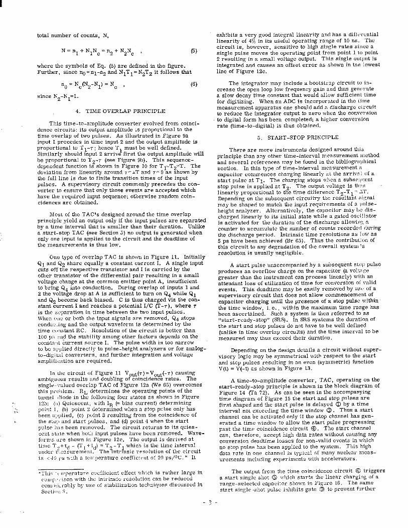
A summary of methods of time-interval measurements is shown in the table.
METHODS OF TIME-INTERVAL MEASUREMENTS IN THE SUBNANOSECOND REGION
1. Counter
2. Counter f Coincidence
3. Vernier with Single Coincidence,
T<T 1
4. Vernier with Multiple Coincidences,
r>T 1
5. Overlap Coincidence
G. start-stop
7. Microwave
Resolving Time Dynamic Range
2 500 ps
2 200 ps
2 15 ps
2 200 ps
2 5 Ps
2 5 Ps
< 1 ps (5)
No Limit in Principle
No Limit in Principle
-5 500(l)
103 - 104 (1)
500(I)
500(I)
100
(1) Practical limit. (2) Can he improved using auxiliary derandomizing circuit. (3) Can be i:nproved considerably by feedback stabilization. (4) Except at both ends of time range. (5) Depends on frequency used.
Long Term Stability .
Very Good
Very Good
Very Good to Good
Very Good
Poor(‘)
Line Integral
Very Good
Very Good
Very Good
Very Good
Very Good(4’
Very Goodt4)
Good
Poor(‘)
Poor to Good (5)
1285A23
sfferential
Very Good
Good(‘)
Good
Good
Goad(4)
Goad(4)
Poor to Good
- h -
6. PICOSECOND TIME-INTERVAL MEASUREMENTS USING MICROWAVE TECHNIQUES (Gu 73)
This method has the highest resolution, a moderate stability and its use is limited to situations in which the time-interval to be measured shows an intrinsic _ RF structure or where RF modulation may be imposed. Consider acceleration of charged particles such as protons, electrons, etc., by use of radio frequency fields; the phase of the RF field is matched to the velocity of the particles to ensure an accelerating field vector on their passage through the RF accelerating structures (cavities). The net effect results in “bunching” of the charged particles in a narrow phase’space. Thus, for example, in the Stanford 2-mile linear accelerator which operates at 2856 MHz the separa- tion between the bunches is 350 ps and each bunch occupies an RF phase of 5 degrees corresponding to a 5 ps time spread in every 350 ps interval. It follows that charged particles produced in interactions or decays originate with the same time structure. Since the time resolution of the best photomultipliers is about 2 orders of magnitude worse, some other technique has to be used to take full advantage of the narrow time spread of the originating particles. An RF separator operating at the same frequency as the accel- erator microwave structure has the requisite character- istics: a charged particle traversing such a separator will be deflected by a distance that is proportional to the relative RF phase angle that it experiences during its traversal. Time-interval measurements may be made with respect to reference particles that enter the scnarator at an RF chase corresponding to null deflection. Thus a time-interval measurement has now been changed to a position measure- ment which can be effected with verv hieh snatial resolution
I Y 1
using multiwire proportional chambers. A sub-picosecond time-interval resolution was reported using this method (c-u 73).
_ 7. TIME SCALE CALIBRATION
One method of time scale calibration mentioned earlier utilizes a radioactive (e.g. , 6oCo) source to produce pulses at random time intervals. These are applied to the stop channel of a time analyzer while the output of a pulse gener- ator of suitable frequency is applied to the start channel. The random time intervals thus generated are displayed on a pulse-height analyzer display and should produce the same number of counts in each time channel within the statistical fluctuations of the recorded counts per channel. The varia- tions of pulse amplitude generated by the radioactive source intr0cluc.e a limit to the accuracy of these measurements because, ofthe inherent time walk for pulses whose amplitude is in the vicinity of the threshold of the discriminator- shaper circuit that has to be used in the stop channel. The method may be improved through pulse amplitude selection utiliziii: a second discriminator which is set at a higher threshold than the stop channel discriminator to ensure via coincitknce gating that all pulses used for calibration are well above an amplitude where time walk is of no significance. The calibration yields information on differential linearity, from which integral linearity may be easily deduced by observing the slope of number of counts versus PHA channel.
An absolute calibration of channel width is obtained by superposing two peaks on the random time spectrum using a resistively split pulse from a fast pulse generator with a variable delay in one channel. A General Radio Trombone delay line type 874-LTL with a Bishop Instrument Trombone Setter model 011-001 yielded delay measurements to an accuracy of *5 ps in the range of 0 to 32 ns (Ta 69).
A resolution of < 40 ps/channel, fwhm, was obtained (We G.5) w!ien both channels in a start-stop TAC were driven from a .zingle photomultiplier using amplitude selected pulses. A variable delay was inserted in one channel with an adju:;tment resolution of 0.3 mm corresponding to 1 ps.
In a similar method (Ta 6s) a helical air insulntcbtl delay drum was used which was drivenby a small syn&ro- nous motor. Output pulses from a constant frequency pulse generator were fed into two transmission lines one of \rliich included the helical delay, Differential linearity was meas- ured by driving the delay drum over the desired delay region and accumulating the outcoming time spectrum. The delay factor of the drum used was 6.45 ps/s and a pulse frequency of 1 kHz. A differential linearity of 15% over a useful oper- ating region was found and an integral linearity of &O. 2% in the same region.
The inherent small time jitter of a sampling sweep in a sampIing type scope provided a simple method tar time calibration down to the ps region (Ch 70). The method used the delayed sampling pulses that were obtained with help of two auxiliary signal pickoff circuits that are attached to a commercially available sampling time base.
As seen in Figure 18 every input event starts a fast ramp, these ramps being triggered at successively higher thresholds. Timing pulses are generated at the instnnts of starting a ramp as well as at the threshold (sampling) levels. Thus each event produces a pulse pair with a delay equal to the integral multiple of a time T as shown in the last line of Figure 18. T is variable since it can be set by the scope time-scale setting. For example the minimum setting of a Tektronix 3T77 sampling sweep unit is 200 ps. Thus a minimum T of 2 ps may be obtained at a setting of 200 ps/ 100 sampling points. The pulse pairs thus generatctl nre applied as start and stop signals, respectively, to :i time- to-pulse-height converter as shown in Figure 19. A signal source is required to trigger the ramp but any signal source is suitable since the time interval between pulse pairs is relatively independent of the input pulse distribution (see interval 3T, third line of Figure 18). The problem of inherent integral non-linearily of the fast ramp may be over- come by use of only the linear portion of the ramp since the number of calibration peaks is much smaller than the number of pulse pairs generated at each sweep.
Calibration results are shown in Figure 20. The upper spectrum was obtained with random input pulses while the lower two spectra were obtained with periodic input pulses. The time scale change was effected by changing the setting of the scope. For example, with a Tektronix 3T77 sweep unit calibration peaks with intervals of up to 1 ps are achievable.
A random-time, random-amplitude generator is des- cribed by Dechamps et al. (De 70) where it is shown that with -- rather simple transfer functions such as RC integration or differentiation a transformation of a Poisson distribution into a uniform distribution may be achieved. To generate random-time pulses with a Poisson distribution the noise of an operation& amplifier, type PA 702 was used.
8. STABILIZATION OF TIME-INTERVAL MEASUREMENTS
In the previous sections we have discussed time-interval measurements with a resolution < 10 1~s. This quantity is about two orders of magnitude lower than the transition times of the semiconductors used in the measurements. Such measurements are quite often of long duration to ensure better statistical results especially when the cross sections of the events to be investigated are very small.
Time-interval measuring systems are subject to noise and to slow drifts of component values, propagation delay times, and temperature dependent parameters. The noise problem is usually reduced through careful shielding of those components exhibiting the fastest transistion times, to minimize their radiation effects. Also, these components are well decoupled irom common power supply lines and a low impedance ground bus is mandatory. Special care must
I
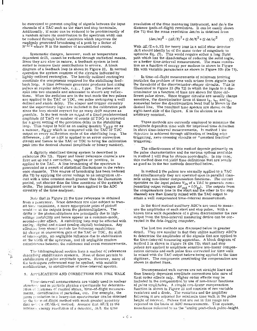
be exercised to prevent coupling of signals between the input channels of a TAC such as the start and stop terminals. Additionally, if noise can be reduced to be predominantly of a random nature its contribution to the spectrum width can be reduced through better statistics which improves the randomly generated broadening of a peak by a factor of N-Ii2 where N is the number of accumulated counts.
Systematic changes, however, such as temperature dependent drift, cannot be reduced through statistical means. Since they are slow in nature, a feedback system is best suited to remove their contributions to errors. A block diagram of a feedback loop is shown in Figure 21. In normal operation the system consists of the circuits indicated by lightly outlined rectangles. The heavily outlined rectangles constitute the components required for the stabilizing feed- back loop. A time reference generator produces fast rising pulses at regular intervals, e.g., 1 pps. The pulses are split into two channels and attenuated to absorb any reflec- tions. When the switches are in the test mode the two pulses are applied to the TAC or TDC, one pulse undergoing a well defined and stable delay. The shaper and trigger circuitry and the supervisory logic are included in the calibration path since the loop should correct for as many drift sources as possible. In the test mode an output of a fixed predetermined amplitude (if TAC) or number of counts (if TDC) is expected for a given setting of the precision delay in the stabilizing loop. This output is held as an analog quantity VREF or as a number, NREE which is compared with the TAC or TDC output on every calibration cycle of the stabilizing loop. The difference, f AV or *AN is applied to an error correction circuit and thence to the TAC or TDC to bring the calibration peak into the desired channel (amplitude or binary number).
A digitally stabilized timing system is described in reference (Ka 72). Upper and lower reference channels are first set up and a correction, negative or positive, is applied to the TAC. A line broadening of the spectrum is generated as a result of statistical fluctuations in the refer- ence channels. This source of broadening has been reduced (Ka 72) by applying the error voltage to an integration cir- cuit with a time constant much greater than the fluctuation period, yet shorter than the time constants of the system’s drifts. The integrated error is then applied to the ADC circuitry of the time analyzer.
Note that in Figure 21 the time reference is obtained from a scnerator. Since detectors are also subject to tran- sit time, variations, a more appropriate point of pickoff would I ‘I’ at the outputs from the photomultipliers. The drifts il. the photomultipliers are principally due to high- voltage instability and hence appear 3s a common-mode, second-order effect. A stabilizing loop may be effected with analog% tligital and mixed (analog-digital) techniques. Any effcctivL> loop shoulcl include the following capabilities: (a) change in conversion gain of the TAC or TDC, (IJ) shift of intcr(>cpt(s), (c) negligillle influence due to stabilization on the \;?dth of the spectrum, and (d) negligible random coincirlcnces between the reference and event measurements.
The> bibliographical section lists a number of references describing stabilization systems. Most of these pertain to stabilization of pulse amplitude spectra. However, many of the techniques referenced may be applied, with suitable mochfic:itions, to stabilization of time-interval spectra.
9. Al’l’LICATIONS AND CORRECTIONS FOR TIME WALK
Tillic-interval measurements are widely used in nuclear struci:~I.~~ and in particle physics experiments for determin- ation r)! Lifetimes of excited states, time-of-flight mensure- merits, Itientification of particles, etc. For example, the mass ri,solution in a heavy-ion spectrometer can be obtained by the !, Irtc-of-flight method with much greater accuracy than u~i~:~: a dE/dX-C method. Assume that m/E is the int~insi~~ energy resolution of a detector, At/t the time
resolution of the time measuring instrument, and As/s the distance (path-of-flight) resolution. It can be easily shown (Ge 71) that the mass resolution Am/m is obtained from
(Am/m)2 = (AE/E)2+ (2 At/t)2+ (2 A~/s)~ (7)
With AE/E N 0.5% for heavy ions in a solid state detector At/t should ideally be of the same order of magnitude to optimize Eq. (7). This would require either a long flight path which has the disadvantage of reducing the solid angle, or a better time-interval measurement. The mass resolu- tion as a function of energy per nucleon is shown in Figure 22a with variable parameters as shown in Figure 221~ (Ce 71).
In time-of-flight measurements of minimum ionizing particles the problem of time walk arises from signals near the threshold of the discriminator-shaper circuits. This is illustrated in Figure 23 (Ba 72) in which the inputs to a dis- criminator as a function of time are shown for three dif- ferent pulse sizes. Since trigger circuits are usually charge sensitive, the discriminator fires at times t somewhat below the discrimination level tha !‘.
t2, and t3, IS shown by the
dashed line. The resultant time spectra are shown on the right-hand side of the figure. K in the abcissa is an arbitrary constant.
Three methods are currently employed to minimize the amplitude dependent time walk for improved time dcfi nition in short time-interval measurements. In method 1 the objective is achieved through utilization of leading edge triggering, zero crossing circuits or “constant fraction” triggering.
The effectiveness of this method depends primarily on the pulse characteristics and the various options available in method 1 will thus be chosen accordingly. In any case, this method does not yield time definitions that are ncnrly as good as in the two methods described below.
In method 2 the pulses are normally applied to a TAC and simultaneously they are operated upon in parallel chan- nels using non-linear compensation functions. The circuit overates on the invut oulses V;,. of a TAC to seneratc com- pensating output voltages AV,i;= f Cvin). Th; outputs from the compensators (one in the start and the other in the stop channel) are then &early mixed with the TAC output to - attain a well compensated time-interval measurement.
In the third method auxiliary ADC’s are used to meas- ure the amplitudes of each start and stop pulse. With a known time walk dependence of a given discriminator the raw output from the time-interval measuring device can be cor- rected in the data-logging computer.
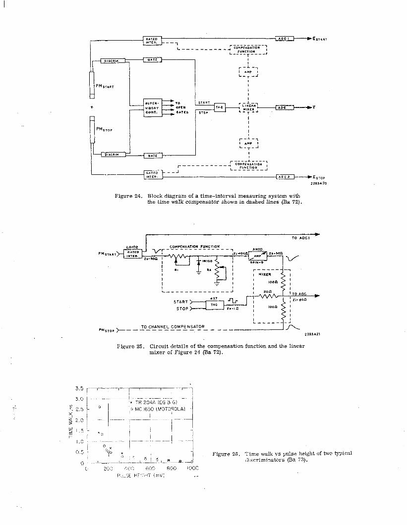
The last two methods are discussed below in greater detail. They are simiIar in that they utilize auxiliary ADC’s to determine the amplitudes of the signals that are applied to the time-interval measuring apparatus. A block diagram of method 2 is shown in Figure 24 (Ba 72); start and stop pulses are applied to amplitude sensitive non-linear compen- sation circuits and each pulse thus corrected for time walk is mixed with the TAC output before being applied to the time digitizer. The components constituting the compensation are shown in dashed lines.
Uncompensated walk curves are not straight lines and thus linearly dependent amplitude corrections take care of first order effects only. Higher order effects may be included in the compensation by use of non-linear functions of pulse amplitudes. A simple non-linear compensation function is shown in Figure 25 and consists of two variable resistors and a diode. The resistors and the amplifier following it are adjusted for minimum time walk in the pulse height of interest. Pulses that arc not in that range are rejected on the basis of ADC measurements. This system, sometimes referred to as the “analog post-clock pulse-height
compensator” is simple to implement and has improved the time walk by a factor of 20 (down to 3+3 ps) over a limited energy range (Ba 72).
Since the uncompensated time walk is very nearly a logarithmic function, compensation over a broad energy range should be possible using active circuits.
The third method in minimizing the time walk problem is of a more general nature. The typical response of two discriminator circuits is shown in Figure 26 (Ba 73). When the amplitude applied to the discriminator is known, correc- tions may be derived from the known or previously calibrated time-walk versus input-amplitude relationship. The tech- nique is especially adapted to computer controlled data- acquisition systems since errors due to time walk can be corrected by the data logging computer before the time spectrum is established, This technique, for example, has been extensively used in K” decay studies (En 71, Ak 72, Pi 72) utilizing a circuit that is capable of measuring ampli- tude as well as time intervals with a resolution < 100 ps in time and < 0.5% in amplitude (PO 69, PO 71).
ACKNOWLEDGEMENTS
Thanks are due to Ray Larsen, Arpad Barna, Bill Jackson, Fred Kirsten and Richard Spitzer for fruitful dis- cussions. I am indebted to Dave Hitlin and Steve Shapiro for reading the manuscript and for their constructive comments.
BIBLIOGRAPHY FOR SUB-NANOSECOND TIME-INTERVAL MEASUREMENTS
Reviews
130 62 M. Bonitz, NIM 22 (1963) 238. Me 68 W. Meiling and F. Story, Nanosecond Pulse Tech-
niques, Gordon and Breach Sci. Publ., 1968, Section 3.4.
oa 68 A. Ogata, S. J. Tao and J. H. Green. NIM 60 (1968).141.
SC 63 x Schwarzschild. NIM 21 (1963) 1. zu 71 R. Van Zurk, P&c. Int~~Symp: Nucl. Electronics,
Warsaw, September 1971.
Time-to-Digital Converters
Lo 64 I. De Lotto, E. Gatti and F. Vaghi in Proc. Conf. Automatic Acquisition and Reduction of Nuclear Data, EANDC, Karlsruhe, 1964, 291.
Me 66 H-Meyer, NIM 40 (1966) 149. PO 69 1:. Polar, NIM 74 (1969) 315. -
Vernier Principle
Av 70 J. Aveynier and R. Van Zurk, NIM 78 (1970) 161. Bn 57 R. G. Baron, Proc. IRE 45 (1957) 21. Ba 71 R. D. Barton and M. E. I&g, NIM 97 (1971) 359. Co 58 C. Cottini, E. Gatti and F. Vaghi. P%c. Conf.
Nucl. Electronics, Paris, 1958. Ki 66 I?. J. Kindlemann and J. Sunderland. Rev. Sci.
j. Instr. 37 (19GG) 445. ?> Le 59 II. W. zfevre and J. T. Russel, Rev. Sci. Instr.
30 (1959) 159. Y Th 66 y Thenard and G. Victor, NIM 40 (1966) 318.
Ve 66 W. H. Venable, Jr., Rev. Sci. f;;str. 37 (1966) - 1443.
Time Overlap and Start-Stop Principles
Bc G5 J. Bell, S. J. Tao and J. H. Green, NIM 35 (1965) - “13.
Be G33 J. Bell, S. J. Tao and J. H. Green, NIM 36 (1965) - :320.
Be 65b
Bi 72
Br 65 Da 67
Dr 70
Le 71 Og 69 Ta 65
Ta 68 Ta 72 We 65 Wi 63
R. E. Bell in Alpha-Beta-and-Gamma-Ray Spectroscopy, Ed. K. Siegbahn, North-Holland Publ. Co., Amsterdam, 1965. J. Bialkowski and M. Moszynski, NIM 105 (1972) - 51. H. Brafman, NIM 34 (1965) 239. C. Dardini, G. IacT M. Lo Savio and R. Visentin, NIM 47 (1967) 233. T. liege, IEEE Trans. Nucl. Sci. NS-17 (1970) 445. LeCroy Research Systems, LRS 2226A (1971). A. Ogata and S. J. Tao, NIM 69 (1969) 344. S. J. Tao, J. Bell and J. H. (&en, NIM 35 (1965) - 222. A. Tamminen and P. Jauho, NIM 65 (1968) 132. I. J. Taylor andT. H. Becker, N% 99 (1972) 387. H. Weisberg, NIM 32 (1965) 133. - D. L. Wieber, NIM?4 (1963) 269. -
Picosecond Time Intervals
Gu 73 Z. G. T. Guiragossian g &. , 1973 Particle Accel- erator Conf., San Francisco, California, 1973; Report No. HEPL 705, Stanford University (1973).
Delay and Time Scale Calibration
Ba 68 C. A. Baker, C. J. Batty and L. E. Williams, NIM 59 (1968) 125.
Be 69 M. Bertolaccini and S. Cova, Proc. Ispra Nucl. Electronics Symp., May 1969, 119.
Ch 67 Z. H. Cho, L. Giedefeldand L. Eriksson, NIM 52 - (1967) 120.
Ch 70 De 70
Z. H. Cho and C. Bohm, NIM E (1970) 327. J. Dechamps, A. Hrisoho and B. Soucek, NIM 84 (1970) 253.
Jo 68 F. A. Johnson, NIM 59 (1968) 237. La 68 A. Langsford and P. E Dolley, NIM 59 (1968) 125. Ta 69 - H. E. Taylor, MM 68 (1969) 160. -
Spectrum Stabilization Methods
Ge 66 E. A. Gere and G. L. Miller, IEEE Trans. Nucl. Sci. NS-13, No. 3 (1966) 508.
Gr 70 J. Grinberg, B. Sabbah and M. Shuster, NIM 82 (1970) 278.
Ka 71 Y. Kawarasaki and T. Shoji, MM 96 (1971) 347. Ka 72 L. Karlsson, NIM 105 (1972) 349. - Le 70 F. R. Lenkszus and J. Rudnick, IEEE Trans.
.Ma 69 Nucl. Sci. NS-17, No. 1 (1970) 285. M. Matoba and I. Kumabe. NIM 74 (1969) 70.
Na 65 M. Nakamura and L. La Pierre, NIM- 32’(1965) 277. Pa 66 A. Pakkanen and F. Stenman, NIM 44 m66) 321. Ro 69 L. B. Robinson and F. S. Goulding-M 75 (1969) -
117. Wi 66 D. Williams, G. F. Snelling and J. Pickup, NIM
39 (1966) 141. -
Applications and Corrections for Time Walk
Ak 72 G. Akavia g 2. , Report No. SLAC-145, Stanford Linear Accelerator Center (1972).
Ba 72 R. D. Barton and M. E. King, N!IM 100 (1972) 165. Ba 73 A. Barna, “High Speed Pulse InstrGtation
Techniques, I’ Stanford Linear Accelerator Center (March 31, 1973).
En 71 J. Enstrom et al., Phys. Rev. C 4 (1971) 2629. Fo 68 J. P. Fouan;niJ. P. Passerieux, NIM G (1963)
327. Ge 71 C. K. Gclblte. K. D. Hildebrand andR. Bock, NIM
Jx- (1971) 397: Pi 72 R. Piccioni etg., Phys. Rev. Lett. 29 (1972) 1412. PO 69 D. Porat and K. Hense, NIM 67 (1969) 229. PO 71 D. Porat and D. Ouimette, Report Nos. SLAC-TN-
71-13, SLAC-TN-71-14, Stanford Linear Acceler- ator Center (June 1971).
DAN I. PORAT obtained his M. SC. in Physics and Ph. D. in EE from the Manchester University, England. He was a Research Fellow at Harvard University (195942) and since 1962 has been on the staff of the Stanford Linear Accelerator Center, Stanford University. Dr. Porat specializes in nuclear instrumentation design including real time data- acquisition systems for scientific research. He is a Senior Member of the IEEE and has published 30 papers. He is co-author with Dr. A. Barna of Integrated Circuits in Digital Electronics (Wiley-Interscience, New York, 1973).
-3-
START
STOP
n
TI T9
L
TIME MARKER GENERATOR GATE T
INPUT TO --I b--T COUNTER 1111111111111111
Figure 1. Time-to-digital converter; timing diagram.
-IT+- PHASE I _--m--- INPUT TO COUNTER I
PHASE 2 ---~---INPUT TO COUNTER 2
Figure 2. The resolution of a TDC is improved by a factor of 2 utilizing two oscillators that are synchronized to start on opposite phases. Two counters are required.
STOP
@-T---- 1 I
r--------------~ (
GATED I
START
CIRCUIT ,
I
DIGITAL OUTPUT PROPORTIONAL TO TSTOP-TSTART ne.1
Figure 3. Time-to-digital converter with interpolation circuit to obtain 1 ns resolution using a 125 MHz clock.
START
STOP
START CHANNEL t I OSCILLATOR I I I I I I I I I
0 I T, 2Ti nTI
I ’ STOP CHANNEL , I OSCILLATOR I I I I I I I I I I
0 T T+T2 T+2T2 T+nT,
I 0
t-
I kT
11113.4
Figure 4. Time expansion using the vernier principle.
START CHANNEL +--
SUPERVISORY LOGIC
STOP CHANNEL>-
STOP
INHIBIT
Figure 5. Vernier time-interval measurement circuit; block diagram.
SUPERVISORY LOGIC
L4i
SIGNETICS 5 P 8” BOA End of
R 6 Digitizin --- CLEAR
Figure 6. Vernier time-interval digitizer, VTID; schematic (Ba 71).
START IN 1
MC 1035
ONE SHOT
ONE SHOT 0
FLIP FLOP
OSC AND
DELAY WD
VETO AND START
STOP
COIN AND
COINS-R FF COIN AND DELL
-1 I -J l-l l-l u l-l I- -l i-l n l-l l-l r- -l LJ l-l
l-l r-l r-l i-l l-l l-l r-l n rl l-l r-l p
n n f-l p I r-l n l-l r 1
COIN VETO AND ‘!+--I
VETO ONE SHOT I
VETO FLOP 5
Figure 7. Timing diagram for the VTID shown in Figure 6 (Ba 71).
OSCILLATOR I,T,
OSCILLATOR 2.T2 -,-’ / I ! 1 1 1 1 1 t 1 1 1 1
I T+NT2
, PHASE I I COINCIDENCES I I I
UP COUNTS
DDYi N COUNTS I I I I I I 1 I I 1 t t t t t
COUNTER STATES 0 1 I 12 1 3 1 2 I IO Fi,we 8. Vernier chronotron for T > Tl; timing
diagram.
INPUT I
0 1 !T,
I I
OUTPUT I 0 T T, t- 0 t-
(0) (b ) ,zs,~,
Figure 9. Time-to-amplitude converter, TAC, using the time-overlap principle; timing waveforms.
I OUTPUT
OUTPUT CL T -T
-T 0 +T
T- 1215A8
+
Figure 10. Output amplitude versus delay T in a time-overlap TAC for T1=T2=T.
I b P 1
“(t)+P “BIAS AFTER OVERLAP
f 7 I*
Figure 11. Schematic of a time-overlap TAC. Overlap duration is T-T as shown in Figure 9.

STOP -
V
(b)
1
TD
(a)
START
STOP
VOLTAGE ACROSS TD
SINGLE
T*
I T;! I T’z+td I
I TI +td /-- I
Figure 12. Time overlap TAC yielding a single-valued output (We 65): (a) Schematic (?J) Operating points of the tunnel diode, TD. I =bias current, II, I2 = currents from start and stop C%l nnels, respectively (c) Timing waveforms. The num- bering on the waveform corresponds to the stable operating points of Figure 12b.
START 1
Figure 13. An even function, V(t)=V(-t) is obtained in a start-stop TAC when its circuit is symmetrical with respect to its two inputs.
I IMt
SHAPER
SHAPER 8 LOGIC
Figure 14. Block diagram of a start-ready-stop TAC (Ta 72). Circled numbers refer to timing diagram of Figure 15.
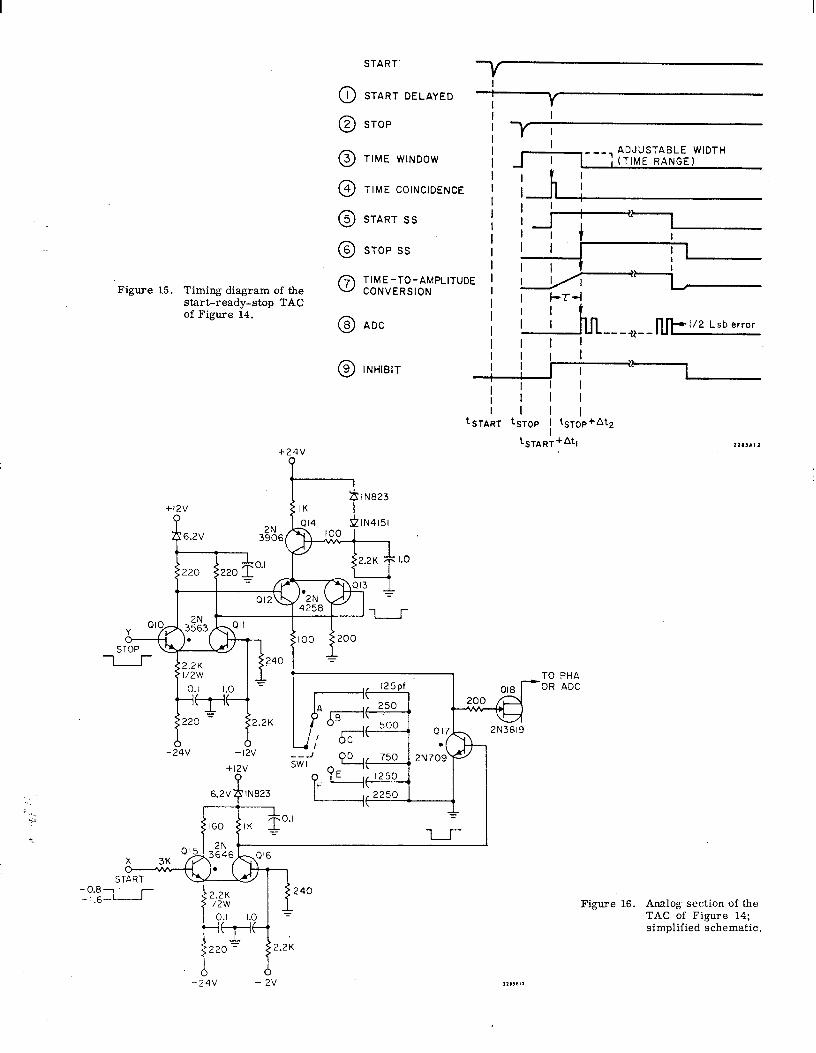
Figure 15. Timing diagram of the 0 start-ready-stop TAC of Figure 14.
@
+24V
P
START
START DELAYED
STOP
TIME WINDOW
TIME COINCIDENCE
START SS
STOP SS
TIME-TO-AMPLITUDE CONVERSION
ADC l/2 Lsb error
I I II INHIBIT I
z
I I I I
I I I
I I I I tSTART hTOP 1 tsToP+&
t.START+Atl 1115*11
l-7 IN823 +12v IK
P A., Ql4 IN4151 6.2V f----r 3%6(?&$f.+,
220 220 T”” ,I, , TO PHA
‘OR ADC
6 b I *I l-l-7 -24V -12
+12v
4
Figure 16. Analog section of the TAC of Figure 14; simplified schematic.
b d -24V -12v

I-
, 0
START
---+-=- I , TIME WINDOW [I ;I
TIME-TO-AMPLIT. ------ CONVERSION
(0) 50 ns range stor1 rote IO MHz 100 ps/chonnel
(c) 1 us range start rote 0.7 MHZ 2 ns/channel
-..-.A-- .- .L 100 200 303 - 403
I I
I. (b) ZOO ns ronge 400 psichonnel
at 4 MHz
I , I EXPANDED SCALE
CtIAPINEL NUMBER
(d) 60 I F
A
.: 5bc I---. G--
,S
B 4
2
-----J
=Lzzzz- 100 5
8 x IO’
6
8 x IO’
6
Figure 17. A series of random time spectra for some of the time ranges of the TAC of Figures 14 and 16. The pulse pair resolution is shown in Figure 17d and was obtained at E 2 pps. The in- trinsic resolution of 60 ps, see peak C, was obtained with an expanded scale.
Figure 18. Principles of sampling scope operation. Upper line shows an input signal with a period 7. The middle line shows the fast ramps generated from the triggers at each positive transition of the input. The horizontal bars show the sam- pling points that are delayed by a time interval T for each successive input. The lower line shows time intervals T,
I 2T . . . nT obtained via pickoff circuits. The dashed wave- form demonstrates that the pulse pair interval is relatively independent of the input pulse distribution.
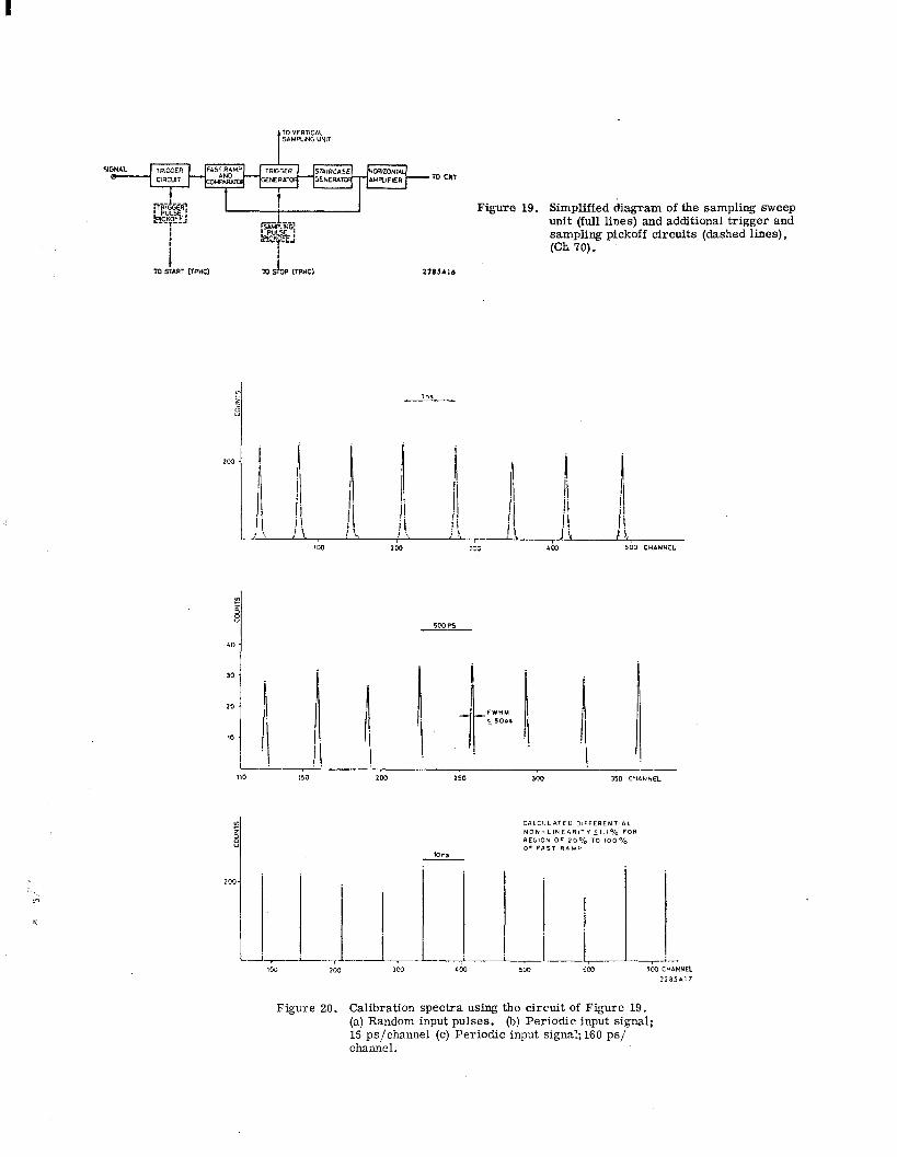
Figure 19. Simplified diagram of the sampling sweep unit (full lines) and additional trigger and sampling pickoff circuits (dashed lines), (Ch 70).
I Figure 20. Calibration spectra using the circuit of Figure 19.
(a) Random input pulses. (b) Periodic input signal; 15 ps/channel (c) Periodic input signal; 160 ps/ channel.

I ANDi3;OGLOR
SUPERVISORY LOGIC
SHAPER Bi TRIGGER
Figure 21. Block diagram of a stabiliziug feedback loop for time-interval measurements.
(a)
Curve 5 Lit number (cm) (Id
I loo 500 2 100 400 3 IW 300 4 loo 200 5 150 500 6 I50 400 7 150 300
Figure 22. (a) Mass resolution of a time-of-flight spectrometer (Ge 71). Abcissa: Energy/atomic mass units
(MeV/amu) Ordinate: Mass resolution Am/m, %. (b) Parameters s and At for the curves of Figure 22a.
(a)
<T> - K-t2 K-tr
(b) ?2teAlP
Figure 23. Time-walk due to three different input pulses applied to a ‘discriminator with a fixed threshold. (a) t the times at which the discriminator fires spectra. IC is an arbitrary constant.
2285A20
Figure 24. Block diagram of a time-interval measuring system with the time walk compensator shown in dashed lines (Ba 72).
I + TO ADCI
TO CHANNEL COMPENSATOR PMSTop)------------------
228SA21
Figure 25. Circuit details of the compensation function and the linear mixer of Figure 24 (Ba 72).
Figure 26. Time walk vs pulse height of two typicnl bcriminators (Ba 73).
230 Si)Q 609 800 1000
P&SE HL’WT ( mV) ,.-,