SubCompact Board GENE-HD05 - EMAC Inc. | Single ... excellent choice for your vital applications....
116
SubCompact Board GENE-HD05 GENE-HD05 AMD ® G-series T56N/T40E/T40R Processor Onboard DDR3 1066/1333 SODIMM 18/24-bit Single/Dual-channel LVDS LCD 8 USB 2.0, 4 COM, 2 SATA, 1 CFast 2 GbE, Mini Card GENE-HD05 Manual Rev. A 2 nd Ed. January 2013
Transcript of SubCompact Board GENE-HD05 - EMAC Inc. | Single ... excellent choice for your vital applications....

SubCompact Board G E N E - H D 0 5
GENE-HD05 AMD® G-series T56N/T40E/T40R
Processor
Onboard DDR3 1066/1333 SODIMM
18/24-bit Single/Dual-channel LVDS LCD
8 USB 2.0, 4 COM, 2 SATA, 1 CFast�
2 GbE, Mini Card
GENE-HD05 Manual Rev. A 2nd Ed. January 2013

SubCompact Board G E N E - H D 0 5
i
Copyright Notice This document is copyrighted, 2013. All rights are reserved. The original manufacturer reserves the right to make improvements to the products described in this manual at any time without notice.
No part of this manual may be reproduced, copied, translated, or transmitted in any form or by any means without the prior written permission of the original manufacturer. Information provided in this manual is intended to be accurate and reliable. However, the original manufacturer assumes no responsibility for its use, or for any in-fringements upon the rights of third parties that may result from its use.
The material in this document is for product information only and is subject to change without notice. While reasonable efforts have been made in the preparation of this document to assure its accuracy, AAEON assumes no liabilities resulting from errors or omissions in this document, or from the use of the information contained herein.
AAEON reserves the right to make changes in the product design without notice to its users.

SubCompact Board G E N E - H D 0 5
ii
Acknowledgments All other products’ name or trademarks are properties of their respective owners.
AMD® is trademark of Advanced Micro Devices.
Microsoft Windows® is a registered trademark of Microsoft Corp.
ITE is a trademark of Integrated Technology Express, Inc.
IBM, PC/AT, PS/2, and VGA are trademarks of International Business Machines Corporation.
All other product names or trademarks are properties of their respective owners.

SubCompact Board G E N E - H D 0 5
iii
Packing List Before you begin installing your card, please make sure that the following materials have been shipped:
Product DVD
GENE-HD05
If any of these items are missing or damaged, please contact your distributor or sales representative immediately.
SubCompact Board G E N E - H D 0 5
iv
Contents
Chapter 1 General Information
1.1 Introduction................................................................... 1-2
1.2 Features ....................................................................... 1-3
1.3 Specifications ............................................................... 1-4
Chapter 2 Quick Installation Guide
2.1 Safety Precautions ....................................................... 2-2
2.2 Location of Connectors and Jumpers .......................... 2-3
2.3 Mechanical Drawing..................................................... 2-5
2.4 List of Jumpers ............................................................. 2-7
2.5 List of Connectors ........................................................ 2-8
2.6 Setting Jumpers ......................................................... 2-10
2.7 Touch Screen 4/5/8-Wire Selection (JP1).................. 2-11
2.8 AT/ATX Power Supply Mode Selection-1 (JP2)......... 2-11
2.9 COM2 Pin8 Function Selection (JP3) ........................ 2-11
2.10 Clear CMOS Selection (JP4) ................................... 2-12
2.11 LVDS Backlight Lightness Up/down Selection (JP5)2-12
2.12 LVDS Operating VDD Selection (JP6) ..................... 2-12
2.13 LVDS Backlight Lightness Control Mode Selection (JP7)
.......................................................................................... 2-13
2.14 LVDS Backlight Inverter VCC Selection (JP8)......... 2-13
2.15 AT/ATX Power Supply Mode Selection-2 (JP9)....... 2-13
2.16 LPC Port (CN1) ........................................................ 2-14

SubCompact Board G E N E - H D 0 5
v
2.17 Touch Screen Connector (CN2)............................... 2-15
2.18 CPU FAN Connector (CN3) ..................................... 2-17
2.19 External +5VSB Input Connector (CN4) .................. 2-18
2.20 External +12V Input Connector (CN5) ..................... 2-18
2.21 Front Panel Connector (CN6) .................................. 2-18
2.22 Digital IO Port Connector (CN7)............................... 2-19
2.23 LPT Port Connector (CN8)....................................... 2-20
2.24 COM Port 2 Connector (CN9) .................................. 2-21
2.25 COM Port 3 Connector (CN10) ................................ 2-23
2.26 COM Port 4 Connector (CN11) ................................ 2-24
2.27 USB 2.0 Ports 7 Connector (CN12) ......................... 2-25
2.28 USB 2.0 Ports 8 Connector (CN13) ......................... 2-25
2.29 USB 2.0 Ports 5 Connector (CN14) ......................... 2-26
2.30 USB 2.0 Ports 6 Connector (CN15) ......................... 2-26
2.31 USB 2.0 Ports 3 Connector (CN16) ......................... 2-27
2.32 USB 2.0 Ports 4 Connector (CN17) ......................... 2-27
2.33 Audio I/O Port Connector (CN18).......................... 2-28
2.34 SATA Port1 Connector (CN19) ................................ 2-28
2.35 SATA Port2 Connector (CN20) ................................ 2-29
2.36 +5V Output for SATA HDD Connector (CN21) ........ 2-30
2.37 LVDS Inverter / Backlight Connector (CN22)........... 2-30
2.38 LVDS Port Connector (CN23) .................................. 2-31
2.39 COM Port 1 (D-SUB 9) Connector (CN24) .............. 2-32
2.40 Realtek LAN (RJ-45) Port2 Connector (CN25) ........ 2-33
2.41 Realtek LAN (RJ-45) Port1 Connector (CN26) ........ 2-34
SubCompact Board G E N E - H D 0 5
vi
2.42 USB Port 1 and 2 Connector (CN27) ....................... 2-34
2.43 HDMI Port Connector (CN28) .................................. 2-35
2.44 PS/2 Keyboard/Mouse Combo Port Connector (CN29)
.......................................................................................... 2-36
2.45 VGA Port Connector (CN30).................................... 2-37
2.46 UIM Card Module Connector (CN32)....................... 2-38
2.47 DDR3 SODIMM Slot (SO-DIMM1) ........................... 2-38
2.48 CFast Slot (CFDA1) ................................................. 2-38
2.49 Mini-Card Slot (PCIEA1) .......................................... 2-39
Chapter 3 AMI BIOS Setup
3.1 System Test and Initialization. ..................................... 3-2
3.2 AMI BIOS Setup ........................................................... 3-3
Chapter 4 Driver Installation
4.1 Installation .................................................................... 4-3
Appendix A Programming The Watchdog Timer
A.1 Programming ............................................................A-2
A.2 F81866 Watchdog Timer Initial Program……………A-5
Appendix B I/O Information
B.1 I/O Address Map.......................................................B-2
B.2 1st MB Memory Address Map ...................................B-4
B.3 IRQ Mapping Chart ...................................................B-5
B.4 DMA Channel Assignments......................................B-7
SubCompact Board G E N E - H D 0 5
vii
Appendix C Mating Connector
C.1 List of Mating Connectors and Cables......................C-2
Appendix D AHCI Setting
D.1 Setting AHCI .............................................................D-2
Appendix E Electrical Specifications for I/O Ports
E.1 Electrical Specifications for I/O Ports........................E-2
SubCompact Board G E N E - H D 0 5
Chapter 1 General Information 1- 1
General
Chapter
1Information

SubCompact Board G E N E - H D 0 5
Chapter 1 General Information 1- 2
1.1 Introduction
AAEON announces a brand new 3.5” SubCompcat Board
GENE-HD05, designed to fit in diverse applications that demand for
fitting in different space limitations and high performance.
GENE-HD05 accommodates onboard AMD® G-series™
T56N/T40E/T40R Processor and features DDR3 SODIMM
1066/1333 system memory up to 4GB. Moreover, GENE-HD05
adopts AMD® A50M chipset to achieve an excellent performance.
In addition, GENE-HD05 deploys Realtek® 8111E Ethernet chip to
feature two RJ-45 ports onboard to display the transcendent
performance of network connections. The display chipset of
GENE-HD05 supports 18/24-bit dual/single channel LVDS LCD and
HDMI function.
In addition to the Mini Card expansion, this model equips two SATA
and one CFast™ for the storage and eight USB 2.0 ports, four COM
ports, 8-bit Digital I/O for flexible I/O expansion. The GENE-HD05 is
an excellent choice for your vital applications.

SubCompact Board G E N E - H D 0 5
Chapter 1 General Information 1- 3
1.2 Features
Onboard AMD® G-series™ T56N/T40E/T40R
Processor, Up to 1.65 GHz
AMD® A50M
DDR3 SODIMM 1066/1333 (T56N) Memory Up to 4 GB
Gigabit Ethernet x 2
18/24-bit Dual/Single Channel LVDS LCD, CRT, HDMI
2CH AC97 2.3 Codec Audio
CFast� x 1, mSATA x 1 (Configured by BIOS), SATA
x 2
USB 2.0 x 8, COM x 4, 8-bit Digital I/O
Mini Card Expansion Interfaces Co-lay mSATA
Function
Supports TPM Module (Optional)
Single DC 12V Input For Easy Power Integration
SubCompact Board G E N E - H D 0 5
Chapter 1 General Information 1- 4
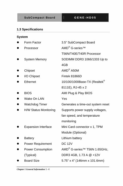
1.3 Specifications
System
Form Factor 3.5” SubCompact Board
Processor AMD® G-series™
T56N/T40E/T40R Processor
System Memory SODIMM DDR3 1066/1333 Up to
4GB
Chipset AMD® A50M
I/O Chipset Fintek 81866D
Ethernet 10/100/1000Base-TX (Realtek®
8111E), RJ-45 x 2
BIOS AMI Plug & Play BIOS
Wake On LAN Yes
Watchdog Timer Generates a time-out system reset
H/W Status Monitoring Supports power supply voltages,
fan speed, and temperature
monitoring
Expansion Interface Mini Card connector x 1, TPM
Module (Optional)
Battery Lithium battery
Power Requirement DC 12V
Power Consumption AMD® G-series™ T56N 1.65GHz,
(Typical) DDR3 4GB, 1.73 A @ +12V
Board Size 5.75” x 4” (146mm x 101.6mm)
SubCompact Board G E N E - H D 0 5
Chapter 1 General Information 1- 5
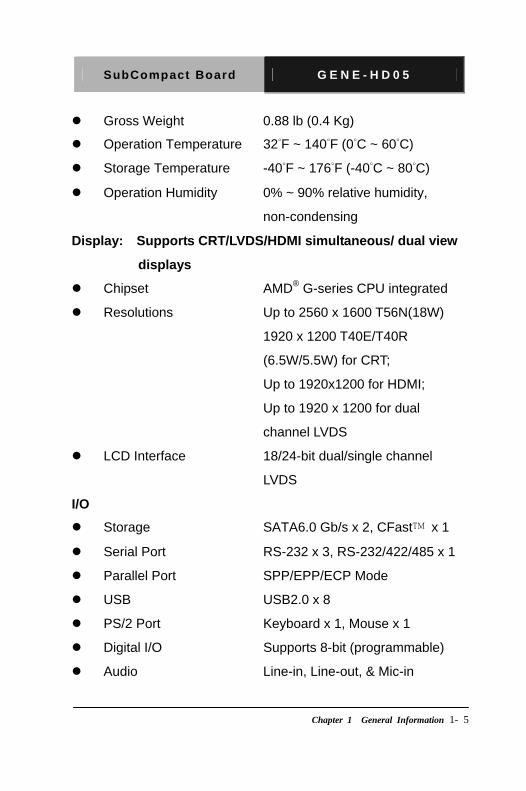
Gross Weight 0.88 lb (0.4 Kg)
Operation Temperature 32°F ~ 140°F (0°C ~ 60°C)
Storage Temperature -40°F ~ 176°F (-40°C ~ 80°C)
Operation Humidity 0% ~ 90% relative humidity,
non-condensing
Display: Supports CRT/LVDS/HDMI simultaneous/ dual view
displays
Chipset AMD® G-series CPU integrated
Resolutions Up to 2560 x 1600 T56N(18W)
1920 x 1200 T40E/T40R
(6.5W/5.5W) for CRT;
Up to 1920x1200 for HDMI;
Up to 1920 x 1200 for dual
channel LVDS
LCD Interface 18/24-bit dual/single channel
LVDS
I/O
Storage SATA6.0 Gb/s x 2, CFast� x 1
Serial Port RS-232 x 3, RS-232/422/485 x 1
Parallel Port SPP/EPP/ECP Mode
USB USB2.0 x 8
PS/2 Port Keyboard x 1, Mouse x 1
Digital I/O Supports 8-bit (programmable)
Audio Line-in, Line-out, & Mic-in
SubCompact Board G E N E - H D 0 5
Chapter 2 Quick Installation Guide 2-1
Quick Installation
Guide
Chapter
2
SubCompact Board G E N E - H D 0 5
Chapter 2 Quick Installation Guide 2-2
2.1 Safety Precautions
Always completely disconnect the power cord from your board whenever you are working on it. Do not make connections while the power is on, because a sudden rush of power can damage sensitive electronic components. Always ground yourself to remove any static charge before touching the board. Modern electronic devices are very sensitive to static electric charges. Use a grounding wrist strap at all times. Place all electronic components on a static-dissipative surface or in a static-shielded bag when they are not in the chassis
SubCompact Board G E N E - H D 0 5
Chapter 2 Quick Installation Guide 2-3
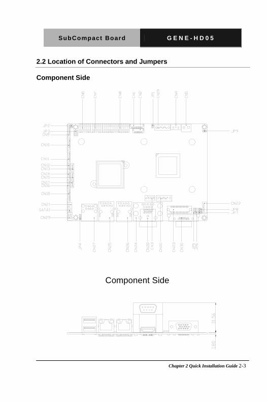
2.2 Location of Connectors and Jumpers
Component Side
Component Side
SubCompact Board G E N E - H D 0 5
Chapter 2 Quick Installation Guide 2-4
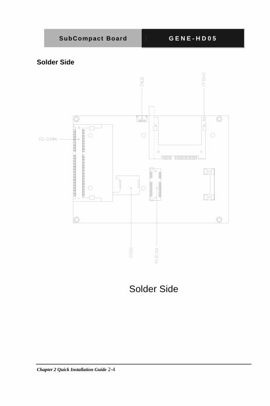
Solder Side
Solder Side

SubCompact Board G E N E - H D 0 5
Chapter 2 Quick Installation Guide 2-5
2.3 Mechanical Drawing
Component Side
Component Side

SubCompact Board G E N E - H D 0 5
Chapter 2 Quick Installation Guide 2-6
Solder Side
Solder Side
SubCompact Board G E N E - H D 0 5
Chapter 2 Quick Installation Guide 2-7
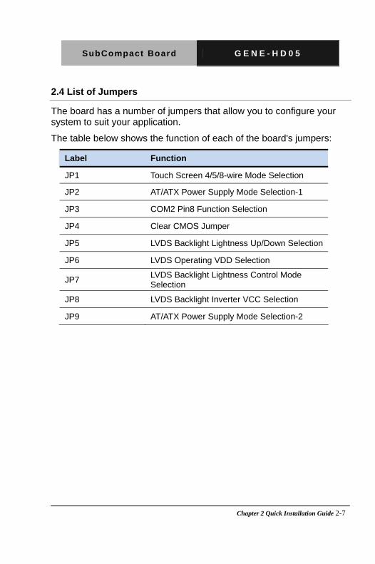
2.4 List of Jumpers
The board has a number of jumpers that allow you to configure your system to suit your application.
The table below shows the function of each of the board's jumpers:
Label Function
JP1 Touch Screen 4/5/8-wire Mode Selection
JP2 AT/ATX Power Supply Mode Selection-1
JP3 COM2 Pin8 Function Selection
JP4 Clear CMOS Jumper
JP5 LVDS Backlight Lightness Up/Down Selection
JP6 LVDS Operating VDD Selection
JP7 LVDS Backlight Lightness Control Mode Selection
JP8 LVDS Backlight Inverter VCC Selection
JP9 AT/ATX Power Supply Mode Selection-2

SubCompact Board G E N E - H D 0 5
Chapter 2 Quick Installation Guide 2-8
2.5 List of Connectors
The board has a number of connectors that allow you to configure your system to suit your application. The table below shows the function of each board's connectors:
Label 0BFunction
CN1 LPC Port
CN2 Touch Screen Connector
CN3 CPU FAN
CN4 External +5VSB Input
CN5 External +12V Input
CN6 Front Panel Connector
CN7 Digital IO Port
CN8 LPT Port
CN9 COM Port 2
CN10 COM Port 3
CN11 COM Port 4
CN12 USB 2.0 Ports 7
CN13 USB 2.0 Ports 8
CN14 USB 2.0 Ports 5
CN15 USB 2.0 Ports 6
CN16 USB 2.0 Ports 3
CN17 USB 2.0 Ports 4
CN18 Audio I/O Port
CN19 SATA Port1 Connector
CN20 SATA Port 2 Connector

SubCompact Board G E N E - H D 0 5
Chapter 2 Quick Installation Guide 2-9
CN21 +5V Output for SATA HDD
CN22 LVDS Inverter / Backlight Connector
CN23 LVDS Port
CN24 COM Port 1 (D-SUB 9)
CN25 Realtek LAN (RJ-45) Port 2
CN26 Realtek LAN (RJ-45) Port 1
CN27 USB Ports 1 and 2
CN28 HDMI Port
CN29 PS/2 Keyboard/Mouse Combo Port
CN30 VGA Port
CN31 SPI Flash JTAG
CN32 UIM Card Module
SO-DIMM1 DDR3 SODIMM Slot
CFDA1 CFast Slot
PCIEA1 Mini-Card Slot

SubCompact Board G E N E - H D 0 5
Chapter 2 Quick Installation Guide 2-10
2.6 Setting Jumpers
You configure your card to match the needs of your application by
setting jumpers. A jumper is the simplest kind of electric switch. It
consists of two metal pins and a small metal clip (often protected by a
plastic cover) that slides over the pins to connect them. To “close” a
jumper you connect the pins with the clip.
To “open” a jumper you remove the clip. Sometimes a jumper will have
three pins, labeled 1, 2 and 3. In this case you would connect either
pins 1 and 2 or 2 and 3.
1 2 3
Open Closed Closed 2-3
A pair of needle-nose pliers may be helpful when working with jumpers.
If you have any doubts about the best hardware configuration for your
application, contact your local distributor or sales representative before
you make any change.
Generally, you simply need a standard cable to make most
connections.
SubCompact Board G E N E - H D 0 5
Chapter 2 Quick Installation Guide 2-11
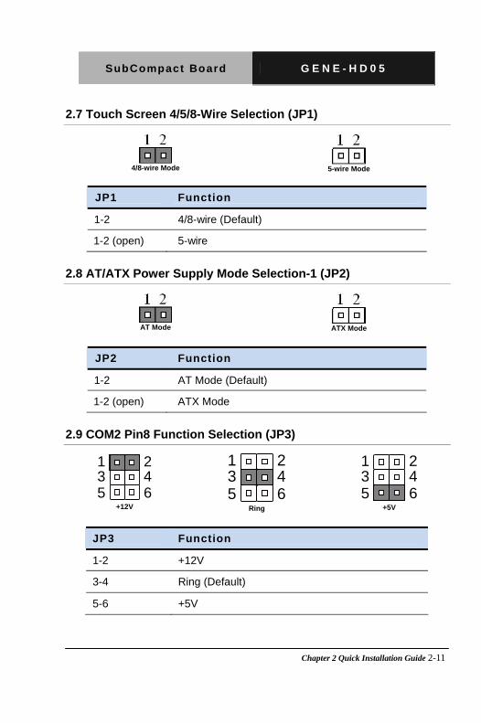
2.7 Touch Screen 4/5/8-Wire Selection (JP1)
4/8-wire Mode
5-wire Mode
JP1 2BFunction
1-2 4/8-wire (Default)
1-2 (open) 5-wire
2.8 AT/ATX Power Supply Mode Selection-1 (JP2)
AT Mode
ATX Mode
JP2 3BFunction
1-2 AT Mode (Default)
1-2 (open) ATX Mode
2.9 COM2 Pin8 Function Selection (JP3)
1 23 45 6
+12V
1 23 45 6
Ring
1 23 45 6
+5V
JP3 1BFunction
1-2 +12V
3-4 Ring (Default)
5-6 +5V
SubCompact Board G E N E - H D 0 5
Chapter 2 Quick Installation Guide 2-12
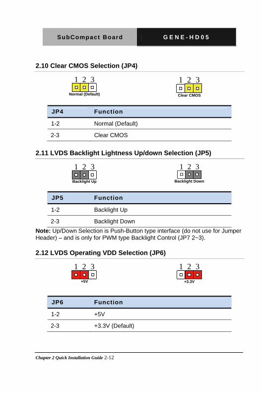
2.10 Clear CMOS Selection (JP4)
1 2 3
Normal (Default)
1 2 3
Clear CMOS
JP4 4BFunction
1-2 Normal (Default)
2-3 Clear CMOS
2.11 LVDS Backlight Lightness Up/down Selection (JP5)
1 2 3
Backlight Up
1 2 3
Backlight Down
JP5 5BFunction
1-2 Backlight Up
2-3 Backlight Down
Note: Up/Down Selection is Push-Button type interface (do not use for Jumper Header) – and is only for PWM type Backlight Control (JP7 2~3).
2.12 LVDS Operating VDD Selection (JP6)
1 2 3
+5V
1 2 3
+3.3V
JP6 6BFunction
1-2 +5V
2-3 +3.3V (Default)
SubCompact Board G E N E - H D 0 5
Chapter 2 Quick Installation Guide 2-13
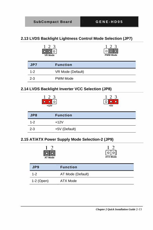
2.13 LVDS Backlight Lightness Control Mode Selection (JP7)
1 2 3
VR Mode
1 2 3
PWM Mode
JP7 7BFunction
1-2 VR Mode (Default)
2-3 PWM Mode
2.14 LVDS Backlight Inverter VCC Selection (JP8)
1 2 3
+12V
1 2 3
+5V
JP8 8BFunction
1-2 +12V
2-3 +5V (Default)
2.15 AT/ATX Power Supply Mode Selection-2 (JP9)
AT Mode
ATX Mode
JP9 9BFunction
1-2 AT Mode (Default)
1-2 (Open) ATX Mode

SubCompact Board G E N E - H D 0 5
Chapter 2 Quick Installation Guide 2-14
LAD0 1
12
LAD1LAD2LAD3
LFRAME#LRESET#
LDRQ0LDRQ1
SERIRQ
GNDLCLK
+3.3V
2.16 LPC Port (CN1)
Pin Pin Name Signal Type Signal Level
1 LAD0 I/O +3.3V
2 LAD1 I/O +3.3V
3 LAD2 I/O +3.3V
4 LAD3 I/O +3.3V
5 +3.3V PWR +3.3V
6 LFRAME# IN
7 LRESET# OUT +3.3V
8 GND GND
9 LCLK OUT
10 LDRQ0 IN
11 LDRQ1 IN
12 SERIRQ I/O +3.3V

SubCompact Board G E N E - H D 0 5
Chapter 2 Quick Installation Guide 2-15
GND 1
9
TOP EXCITE
BOTTOM EXCITE
LEFT EXCITE
RIGHT EXCITE
TOP SENSE
BOTTOM SENSE
LEFT SENSE
RIGHT SENSE
8 Wires
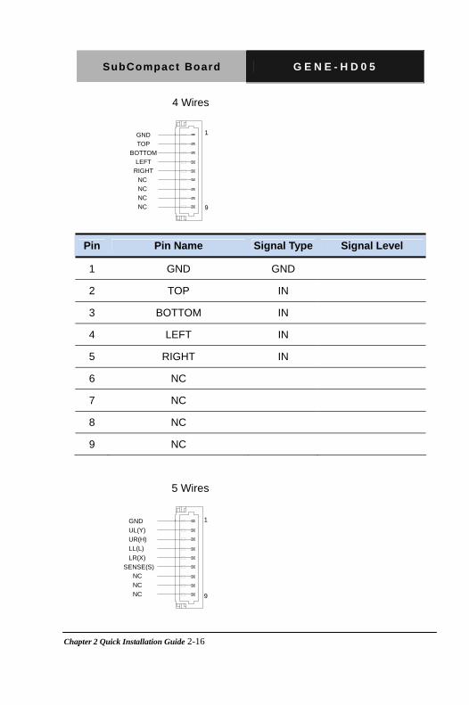
2.17 Touch Screen Connector (CN2)
Pin Pin Name Signal Type Signal Level
1 GND GND
2 TOP EXCITE IN
3 BOTTOM EXCITE IN
4 LEFT EXCITE IN
5 RIGHT EXCITE IN
6 TOP SENSE IN
7 BOTTOM SENSE IN
8 LEFT SENSE IN
9 RIGHT SENSE IN
SubCompact Board G E N E - H D 0 5
Chapter 2 Quick Installation Guide 2-16
1
9
GND
TOP
BOTTOM
LEFT
RIGHT
NC
NC
NC
NC
4 Wires
1
9
GND
UL(Y)
UR(H)
LL(L)
LR(X)
SENSE(S)NC
NC
NC
5 Wires
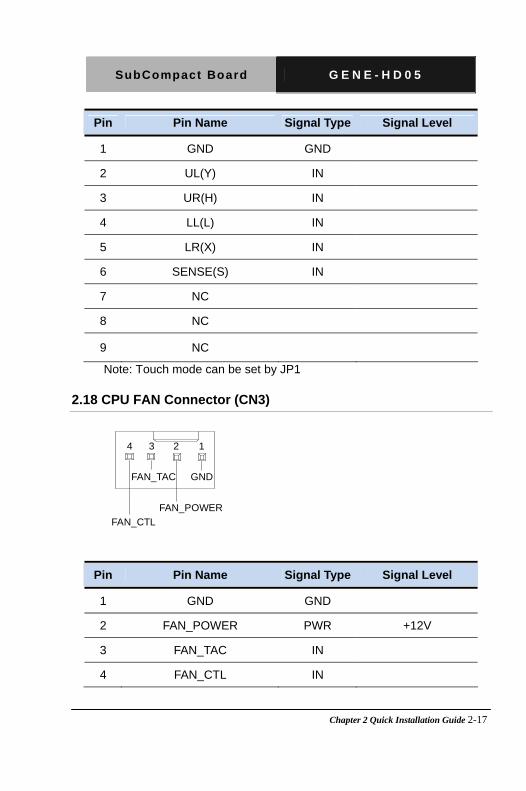
Pin Pin Name Signal Type Signal Level
1 GND GND
2 TOP IN
3 BOTTOM IN
4 LEFT IN
5 RIGHT IN
6 NC
7 NC
8 NC
9 NC
SubCompact Board G E N E - H D 0 5
Chapter 2 Quick Installation Guide 2-17
Pin Pin Name Signal Type Signal Level
1 GND GND
2 UL(Y) IN
3 UR(H) IN
4 LL(L) IN
5 LR(X) IN
6 SENSE(S) IN
7 NC
8 NC
9 NC
Note: Touch mode can be set by JP1
2.18 CPU FAN Connector (CN3)
GND
123
FAN_POWER
FAN_TAC
4
FAN_CTL
Pin Pin Name Signal Type Signal Level
1 GND GND
2 FAN_POWER PWR +12V
3 FAN_TAC IN
4 FAN_CTL IN
SubCompact Board G E N E - H D 0 5
Chapter 2 Quick Installation Guide 2-18
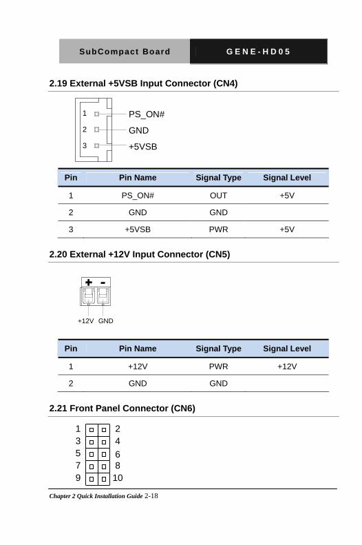
2.19 External +5VSB Input Connector (CN4)
+5VSB
GND
PS_ON#1
2
3
Pin Pin Name Signal Type Signal Level
1 PS_ON# OUT +5V
2 GND GND
3 +5VSB PWR +5V
2.20 External +12V Input Connector (CN5)
+12V GND
Pin Pin Name Signal Type Signal Level
1 +12V PWR +12V
2 GND GND
2.21 Front Panel Connector (CN6)
1 23 45 67 89 10

SubCompact Board G E N E - H D 0 5
Chapter 2 Quick Installation Guide 2-19
Pin Pin Name Signal Type Signal Level
1 PWR_BTN-
2 PWR_BTN+
3 HDD_LED-
4 HDD_LED+
5 SPEAKER-
6 SPEAKER+
7 PWR_LED-
8 PWR_LED+
9 H/W RESET-
10 H/W RESET+
2.22 Digital IO Port Connector (CN7)
1 23 45 67 89 10
Pin Pin Name Signal type Signal Level
1 DIO0 I/O +3.3V
2 DIO1 I/O +3.3V
3 DIO2 I/O +3.3V
4 DIO3 I/O +3.3V
5 DIO4 I/O +3.3V
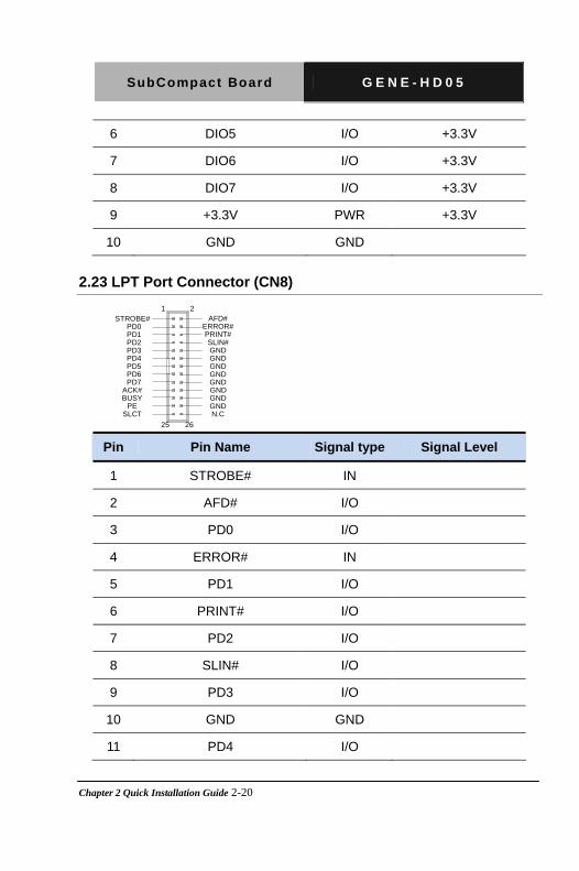
SubCompact Board G E N E - H D 0 5
Chapter 2 Quick Installation Guide 2-20
6 DIO5 I/O +3.3V
7 DIO6 I/O +3.3V
8 DIO7 I/O +3.3V
9 +3.3V PWR +3.3V
10 GND GND
2.23 LPT Port Connector (CN8)
STROBE#1 2
25 26
AFD#ERROR#PRINT#SLIN#GNDGNDGNDGNDGNDGNDGNDGNDN.C
PD0PD1PD2PD3PD4PD5PD6PD7
ACK#BUSY
PESLCT
Pin Pin Name Signal type Signal Level
1 STROBE# IN
2 AFD# I/O
3 PD0 I/O
4 ERROR# IN
5 PD1 I/O
6 PRINT# I/O
7 PD2 I/O
8 SLIN# I/O
9 PD3 I/O
10 GND GND
11 PD4 I/O
SubCompact Board G E N E - H D 0 5
Chapter 2 Quick Installation Guide 2-21
1
2
3
4
5
6
7
8
9
12 GND GND
13 PD5 I/O
14 GND GND
15 PD6 I/O
16 GND GND
17 PD7 I/O
18 GND GND
19 ACK# IN
20 GND GND
21 BUSY IN
22 GND GND
23 PE IN
24 GND GND
25 SLCT IN
26 NC
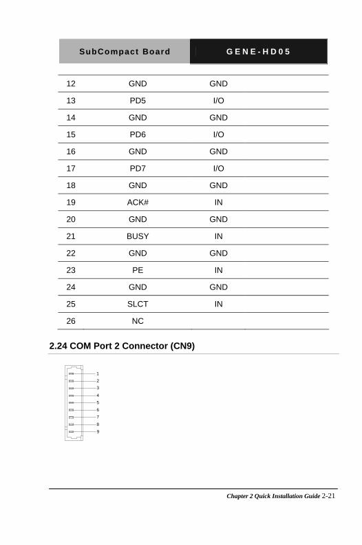
2.24 COM Port 2 Connector (CN9)
SubCompact Board G E N E - H D 0 5
Chapter 2 Quick Installation Guide 2-22
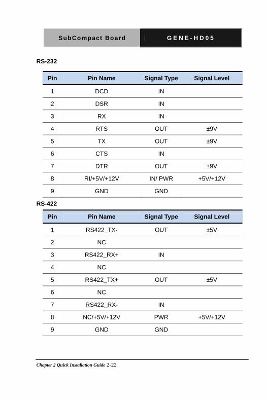
RS-232
Pin Pin Name Signal Type Signal Level
1 DCD IN
2 DSR IN
3 RX IN
4 RTS OUT ±9V
5 TX OUT ±9V
6 CTS IN
7 DTR OUT ±9V
8 RI/+5V/+12V IN/ PWR +5V/+12V
9 GND GND
RS-422
Pin Pin Name Signal Type Signal Level
1 RS422_TX- OUT ±5V
2 NC
3 RS422_RX+ IN
4 NC
5 RS422_TX+ OUT ±5V
6 NC
7 RS422_RX- IN
8 NC/+5V/+12V PWR +5V/+12V
9 GND GND
SubCompact Board G E N E - H D 0 5
Chapter 2 Quick Installation Guide 2-23
RS-485
Pin Pin Name Signal Type Signal Level
1 RS485_D- I/O ±5V
2 NC
3 NC
4 NC
5 RS485_D+ I/O ±5V
6 NC
7 NC
8 NC/+5V/+12V PWR +5V/+12V
9 GND GND
Note: COM2 RS-232/422/485 can be set by BIOS setting. Default is
RS-232. Pin 8 function can be set by Jumper.
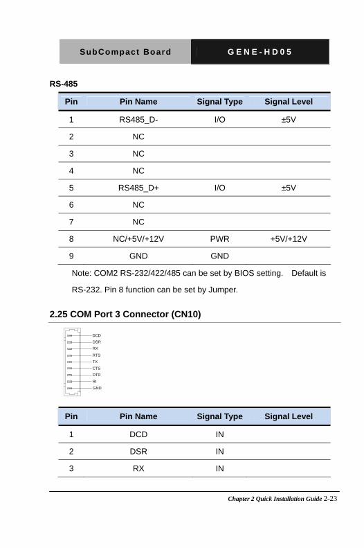
2.25 COM Port 3 Connector (CN10)
Pin Pin Name Signal Type Signal Level
1 DCD IN
2 DSR IN
3 RX IN
DCD
DSR
RX
RTS
TX
CTS
DTR
RI
GND
SubCompact Board G E N E - H D 0 5
Chapter 2 Quick Installation Guide 2-24
4 RTS OUT ±9V
5 TX OUT ±9V
6 CTS IN
7 DTR OUT ±9V
8 RI IN
9 GND GND
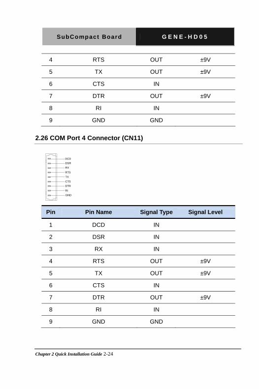
2.26 COM Port 4 Connector (CN11)
Pin Pin Name Signal Type Signal Level
1 DCD IN
2 DSR IN
3 RX IN
4 RTS OUT ±9V
5 TX OUT ±9V
6 CTS IN
7 DTR OUT ±9V
8 RI IN
9 GND GND
DCD
DSR
RX
RTS
TX
CTS
DTR
RI
GND
SubCompact Board G E N E - H D 0 5
Chapter 2 Quick Installation Guide 2-25
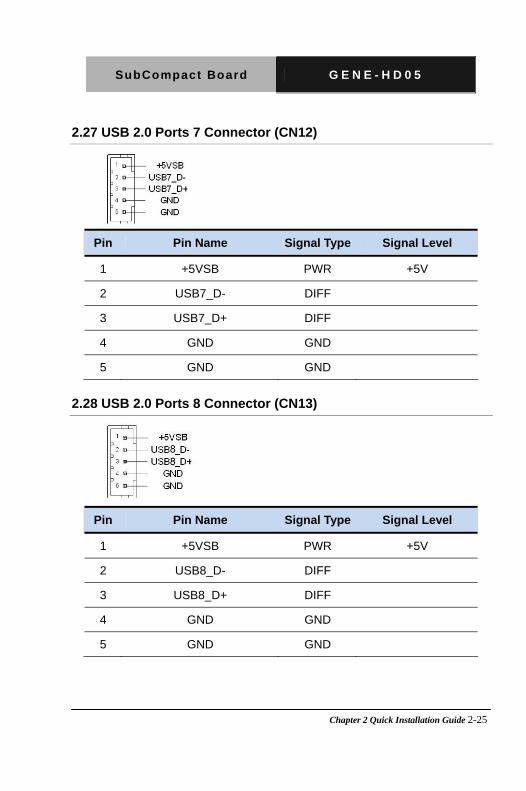
2.27 USB 2.0 Ports 7 Connector (CN12)
Pin Pin Name Signal Type Signal Level
1 +5VSB PWR +5V
2 USB7_D- DIFF
3 USB7_D+ DIFF
4 GND GND
5 GND GND
2.28 USB 2.0 Ports 8 Connector (CN13)
Pin Pin Name Signal Type Signal Level
1 +5VSB PWR +5V
2 USB8_D- DIFF
3 USB8_D+ DIFF
4 GND GND
5 GND GND

SubCompact Board G E N E - H D 0 5
Chapter 2 Quick Installation Guide 2-26
2.29 USB 2.0 Ports 5 Connector (CN14)
Pin Pin Name Signal Type Signal Level
1 +5VSB PWR +5V
2 USB5_D- DIFF
3 USB5_D+ DIFF
4 GND GND
5 GND GND
2.30 USB 2.0 Ports 6 Connector (CN15)
Pin Pin Name Signal Type Signal Level
1 +5VSB PWR +5V
2 USB6_D- DIFF
3 USB6_D+ DIFF
4 GND GND
5 GND GND

SubCompact Board G E N E - H D 0 5
Chapter 2 Quick Installation Guide 2-27
2.31 USB 2.0 Ports 3 Connector (CN16)
Pin Pin Name Signal Type Signal Level
1 +5VSB PWR +5V
2 USB3_D- DIFF
3 USB3_D+ DIFF
4 GND GND
5 GND GND
2.32 USB 2.0 Ports 4 Connector (CN17)
Pin Pin Name Signal Type Signal Level
1 +5VSB PWR +5V
2 USB4_D- DIFF
3 USB4_D+ DIFF
4 GND GND
5 GND GND

SubCompact Board G E N E - H D 0 5
Chapter 2 Quick Installation Guide 2-28
2.33 Audio I/O Port Connector (CN18)
MIC_L1
10
MIC_R
LINE_L_INLINE_R_IN
LEFT_OUT
RIGHT_OUT+5V_AUDIO
GND_AUDIO
GND_AUDIO
GND_AUDIO
Pin Pin Name Signal Type Signal Level
1 MIC_L IN
2 MIC_R IN
3 GND_AUDIO GND
4 LINE_L_IN IN
5 LINE_R_IN IN
6 GND_AUDIO GND
7 LEFT_OUT OUT
8 GND_AUDIO GND
9 RIGHT_OUT OUT
10 +5V_AUDIO PWR +5V
2.34 SATA Port1 Connector (CN19)
Pin 1 Pin 7

SubCompact Board G E N E - H D 0 5
Chapter 2 Quick Installation Guide 2-29
Pin Pin Name Signal Type Signal Level
1 GND GND
2 SATA_TX+ DIFF
3 SATA_TX- DIFF
4 GND GND
5 SATA_RX- DIFF
6 SATA_RX+ DIFF
7 GND GND
2.35 SATA Port2 Connector (CN20)
Pin 1 Pin 7
Pin Pin Name Signal Type Signal Level
1 GND GND
2 SATA_TX+ DIFF
3 SATA_TX- DIFF
4 GND GND
5 SATA_RX- DIFF
6 SATA_RX+ DIFF
7 GND GND
SubCompact Board G E N E - H D 0 5
Chapter 2 Quick Installation Guide 2-30
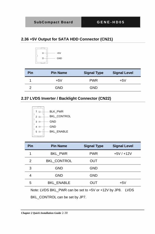
2.36 +5V Output for SATA HDD Connector (CN21)
+5V
GND
Pin Pin Name Signal Type Signal Level
1 +5V PWR +5V
2 GND GND
2.37 LVDS Inverter / Backlight Connector (CN22)
BLK_PWR
2
3
4
5
1
BKL_CONTROL
GND
GND
BKL_ENABLE
Pin Pin Name Signal Type Signal Level
1 BKL_PWR PWR +5V / +12V
2 BKL_CONTROL OUT
3 GND GND
4 GND GND
5 BKL_ENABLE OUT +5V
Note: LVDS BKL_PWR can be set to +5V or +12V by JP8. LVDS
BKL_CONTROL can be set by JP7.

SubCompact Board G E N E - H D 0 5
Chapter 2 Quick Installation Guide 2-31
2.38 LVDS Port Connector (CN23)
PIN 1 PIN 2
PIN 30PIN 29
Pin Pin Name Signal Type Signal Level
1 BKL_ENABLE OUT
2 BKL_CONTROL OUT
3 LCD_PWR PWR +3.3V/+5V
4 GND GND
5 LVDS_A_CLK- DIFF
6 LVDS_A_CLK+ DIFF
7 LCD_PWR PWR +3.3V/+5V
8 GND GND
9 LVDS_DA0- DIFF
10 LVDS_DA0+ DIFF
11 LVDS_DA1- DIFF
12 LVDS_DA1+ DIFF
13 LVDS_DA2- DIFF

SubCompact Board G E N E - H D 0 5
Chapter 2 Quick Installation Guide 2-32
14 LVDS_DA2+ DIFF
15 LVDS_DA3- DIFF
16 LVDS_DA3+ DIFF
17 DDC_DATA I/O +3.3V
18 DDC_CLK I/O +3.3V
19 LVDS_DB0- DIFF
20 LVDS_DB0+ DIFF
21 LVDS_DB1- DIFF
22 LVDS_DB1+ DIFF
23 LVDS_DB2- DIFF
24 LVDS_DB2+ DIFF
25 LVDS_DB3- DIFF
26 LVDS_DB3+ DIFF
27 LCD_PWR PWR +3.3V/+5V
28 GND GND
29 LVDS_B_CLK- DIFF
30 LVDS_B_CLK+ DIFF
Note: LVDS LCD_PWR can be set to +3.3V or +5V by JP6.
2.39 COM Port 1 (D-SUB 9) Connector (CN24)
1 5
6 9

SubCompact Board G E N E - H D 0 5
Chapter 2 Quick Installation Guide 2-33
Pin Pin Name Signal Type Signal Level
1 DCD IN
2 RX IN
3 TX OUT ±9V
4 DTR OUT ±9V
5 GND GND
6 DSR IN
7 RTS OUT ±9V
8 CTS IN
9 RI IN
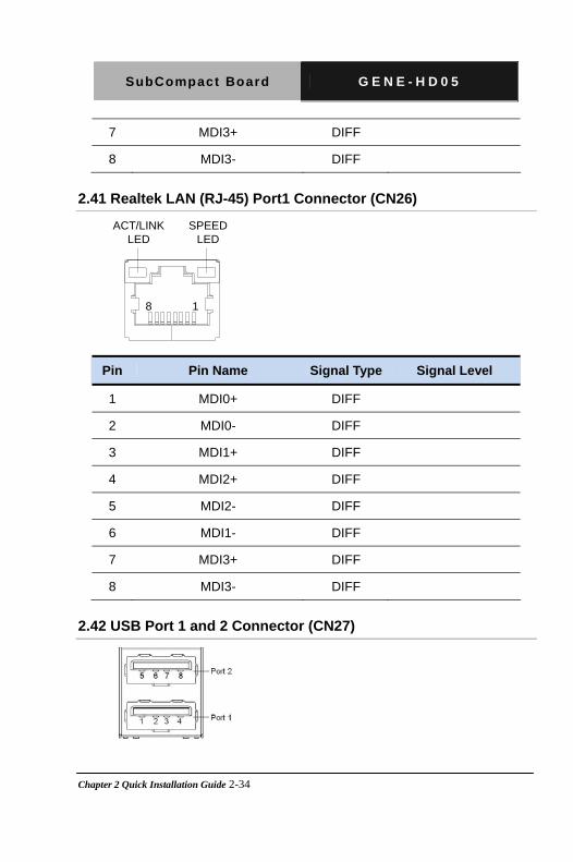
2.40 Realtek LAN (RJ-45) Port2 Connector (CN25)
1
ACT/LINKLED
SPEEDLED
8
Pin Pin Name Signal Type Signal Level
1 MDI0+ DIFF
2 MDI0- DIFF
3 MDI1+ DIFF
4 MDI2+ DIFF
5 MDI2- DIFF
6 MDI1- DIFF
SubCompact Board G E N E - H D 0 5
Chapter 2 Quick Installation Guide 2-34
7 MDI3+ DIFF
8 MDI3- DIFF
2.41 Realtek LAN (RJ-45) Port1 Connector (CN26)
1
ACT/LINKLED
SPEEDLED
8
Pin Pin Name Signal Type Signal Level
1 MDI0+ DIFF
2 MDI0- DIFF
3 MDI1+ DIFF
4 MDI2+ DIFF
5 MDI2- DIFF
6 MDI1- DIFF
7 MDI3+ DIFF
8 MDI3- DIFF
2.42 USB Port 1 and 2 Connector (CN27)

SubCompact Board G E N E - H D 0 5
Chapter 2 Quick Installation Guide 2-35
Pin Pin Name Signal Type Signal Level
1 +5VSB PWR +5V
2 USB1_D- DIFF
3 USB1_D+ DIFF
4 GND GND
5 +5VSB PWR +5V
6 USB2_D- DIFF
7 USB2_D+ DIFF
8 GND GND
2.43 HDMI Port Connector (CN28)
Pin Pin Name Signal Type Signal Level
1 TMDS_Data2+ DIFF
2 GND GND
3 TMDS_ Data2- DIFF
4 TMDS_ Data1+ DIFF
5 GND GND
6 TMDS_ Data1- DIFF
7 TMDS_ Data0+ DIFF
8 GND GND
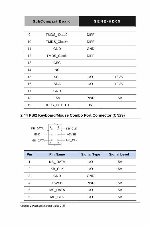
SubCompact Board G E N E - H D 0 5
Chapter 2 Quick Installation Guide 2-36
9 TMDS_ Data0- DIFF
10 TMDS_Clock+ DIFF
11 GND GND
12 TMDS_Clock- DIFF
13 CEC
14 NC
15 SCL I/O +3.3V
16 SDA I/O +3.3V
17 GND
18 +5V PWR +5V
19 HPLG_DETECT IN
2.44 PS/2 Keyboard/Mouse Combo Port Connector (CN29)
KB_CLKKB_DATA1
4 6
2
MS_DATA
+5VSBGND
MS_CLK
Pin Pin Name Signal Type Signal Level
1 KB_ DATA I/O +5V
2 KB_CLK I/O +5V
3 GND GND
4 +5VSB PWR +5V
5 MS_DATA I/O +5V
6 MS_CLK I/O +5V

SubCompact Board G E N E - H D 0 5
Chapter 2 Quick Installation Guide 2-37
2.45 VGA Port Connector (CN30)
Pin Pin Name Signal Type Signal Level
1 RED OUT
2 GREEN OUT
3 BLUE OUT
4 NC
5 GND GND
6 RED_GND_RTN GND
7 GREEN_GND_RTN GND
8 BLUE_GND_RTN GND
9 +5V PWR +5V
10 GND GND
11 NC
12 DDC_DATA I/O +5V
13 HSYNC OUT
14 VSYNC OUT
15 DDC_CLK I/O +5V

SubCompact Board G E N E - H D 0 5
Chapter 2 Quick Installation Guide 2-38
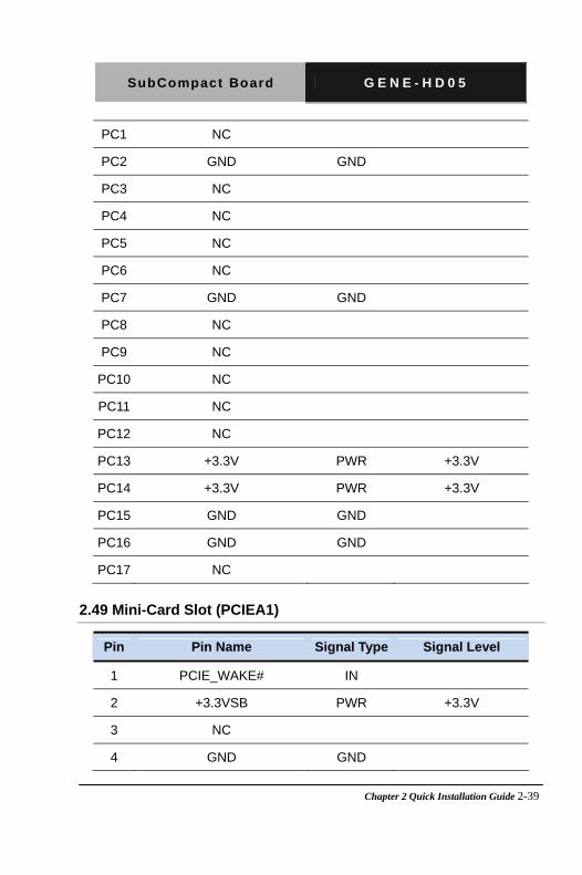
2.46 UIM Card Module Connector (CN32)
Pin Pin Name Signal Type Signal Level
1 UIM_PWR PWR
2 UIM_RST IN
3 UIM_CLK IN
4 GND GND
5 UIM_VPP PWR
6 UIM_DATA I/O
2.47 DDR3 SODIMM Slot (SO-DIMM1)
Standard specification
2.48 CFast Slot (CFDA1)
Pin Pin Name Signal Type Signal Level
S1 GND GND
S2 SATA_TX+ DIFF
S3 SATA_TX- DIFF
S4 GND GND
S5 SATA_RX- DIFF
S6 SATA_RX+ DIFF
S7 GND GND
SubCompact Board G E N E - H D 0 5
Chapter 2 Quick Installation Guide 2-39
PC1 NC
PC2 GND GND
PC3 NC
PC4 NC
PC5 NC
PC6 NC
PC7 GND GND
PC8 NC
PC9 NC
PC10 NC
PC11 NC
PC12 NC
PC13 +3.3V PWR +3.3V
PC14 +3.3V PWR +3.3V
PC15 GND GND
PC16 GND GND
PC17 NC
2.49 Mini-Card Slot (PCIEA1)
Pin Pin Name Signal Type Signal Level
1 PCIE_WAKE# IN
2 +3.3VSB PWR +3.3V
3 NC
4 GND GND
SubCompact Board G E N E - H D 0 5
Chapter 2 Quick Installation Guide 2-40
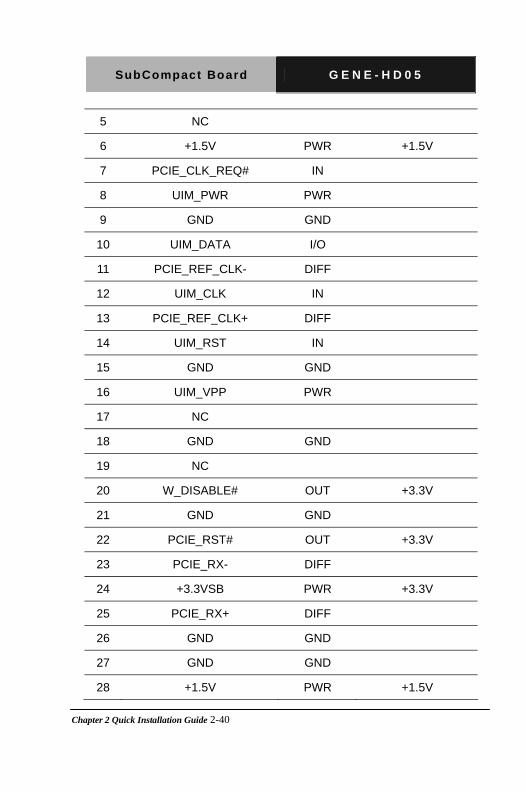
5 NC
6 +1.5V PWR +1.5V
7 PCIE_CLK_REQ# IN
8 UIM_PWR PWR
9 GND GND
10 UIM_DATA I/O
11 PCIE_REF_CLK- DIFF
12 UIM_CLK IN
13 PCIE_REF_CLK+ DIFF
14 UIM_RST IN
15 GND GND
16 UIM_VPP PWR
17 NC
18 GND GND
19 NC
20 W_DISABLE# OUT +3.3V
21 GND GND
22 PCIE_RST# OUT +3.3V
23 PCIE_RX- DIFF
24 +3.3VSB PWR +3.3V
25 PCIE_RX+ DIFF
26 GND GND
27 GND GND
28 +1.5V PWR +1.5V
SubCompact Board G E N E - H D 0 5
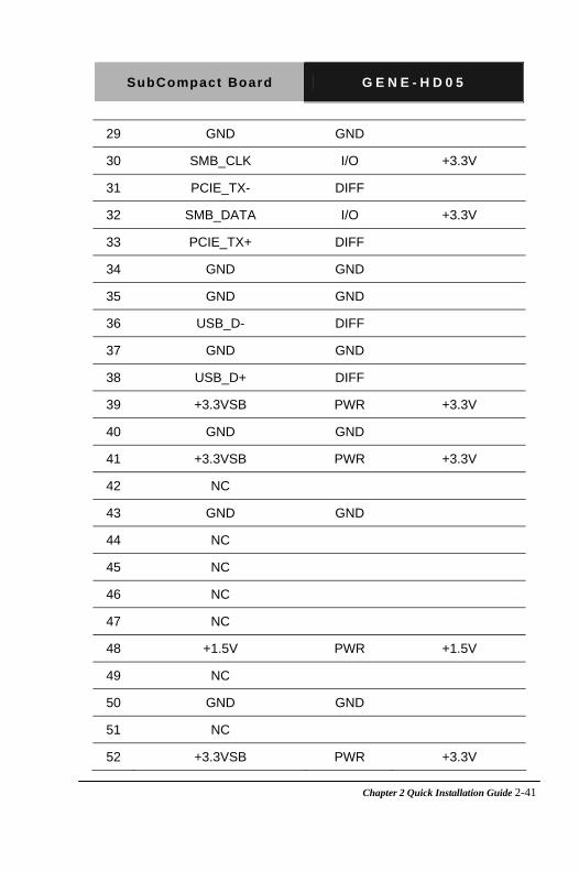
Chapter 2 Quick Installation Guide 2-41
29 GND GND
30 SMB_CLK I/O +3.3V
31 PCIE_TX- DIFF
32 SMB_DATA I/O +3.3V
33 PCIE_TX+ DIFF
34 GND GND
35 GND GND
36 USB_D- DIFF
37 GND GND
38 USB_D+ DIFF
39 +3.3VSB PWR +3.3V
40 GND GND
41 +3.3VSB PWR +3.3V
42 NC
43 GND GND
44 NC
45 NC
46 NC
47 NC
48 +1.5V PWR +1.5V
49 NC
50 GND GND
51 NC
52 +3.3VSB PWR +3.3V

SubCompact Board G E N E - H D 0 5
Chapter 2 Quick Installation Guide 2-42
Below Table for China RoHS Requirements 产品中有毒有害物质或元素名称及含量
AAEON Main Board/ Daughter Board/ Backplane
有毒有害物质或元素
部件名称 铅
(Pb)
汞
(Hg)
镉
(Cd)
六价铬
(Cr(VI))
多溴联苯
(PBB)
多溴二苯醚
(PBDE)
印刷电路板
及其电子组件× ○ ○ ○ ○ ○
外部信号
连接器及线材× ○ ○ ○ ○ ○
O:表示该有毒有害物质在该部件所有均质材料中的含量均在 SJ/T 11363-2006 标准规定的限量要求以下。
X:表示该有毒有害物质至少在该部件的某一均质材料中的含量超出
SJ/T 11363-2006 标准规定的限量要求。 备注:此产品所标示之环保使用期限,系指在一般正常使用状况下。
SubCompact Board G E N E - H D 0 5
Chapter 3 AMI BIOS Setup 3-1
AMI
Chapter
3BIOS Setup
SubCompact Board G E N E - H D 0 5
3.1 System Test and Initialization
These routines test and initialize board hardware. If the routines
encounter an error during the tests, you will either hear a few short
beeps or see an error message on the screen. There are two kinds
of errors: fatal and non-fatal. The system can usually continue the
boot up sequence with non-fatal errors.
System configuration verification
These routines check the current system configuration against the
values stored in the CMOS memory. If they do not match, the
program outputs an error message. You will then need to run the
BIOS setup program to set the configuration information in memory.
There are three situations in which you will need to change the
CMOS settings:
1. You are starting your system for the first time
2. You have changed the hardware attached to your system
3. The CMOS memory has lost power and the configuration
information has been erased.
The GENE-HD05 CMOS memory has an integral lithium battery
backup for data retention. However, you will need to replace the
complete unit when it finally runs down.
Chapter 3 AMI BIOS Setup 3-2

SubCompact Board G E N E - H D 0 5
3.2 AMI BIOS Setup
AMI BIOS ROM has a built-in Setup program that allows users to
modify the basic system configuration. This type of information is
stored in battery-backed CMOS RAM so that it retains the Setup
information when the power is turned off.
Entering Setup
Power on the computer and press <Del> or <F2> immediately. This
will allow you to enter Setup.
Main
Set the date, use tab to switch between date elements.
Advanced Advanced BIOS Features Setup including TPM, ACPI, etc. Chipset Host bridge parameters. Boot Enables/disable quiet boot option. Security Set setup administrator password.
Save&Exit
Exit system setup after saving the changes.
Chapter 3 AMI BIOS Setup 3-3
SubCompact Board G E N E - H D 0 5
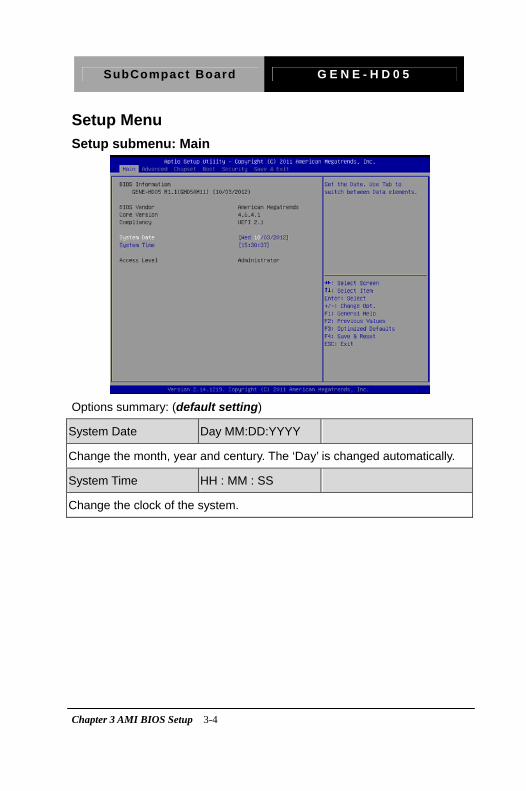
Setup Menu
Setup submenu: Main
Options summary: (default setting)
System Date Day MM:DD:YYYY
Change the month, year and century. The ‘Day’ is changed automatically.
System Time HH : MM : SS
Change the clock of the system.
Chapter 3 AMI BIOS Setup 3-4
SubCompact Board G E N E - H D 0 5
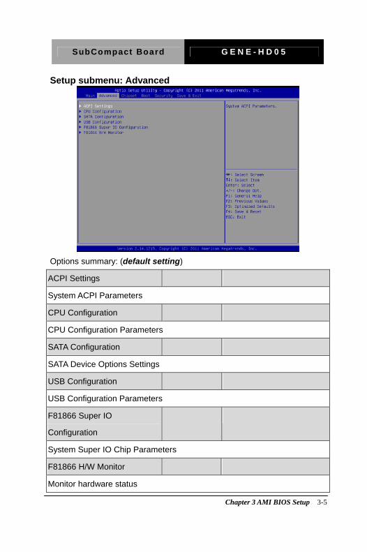
Setup submenu: Advanced
Options summary: (default setting)
ACPI Settings
System ACPI Parameters
CPU Configuration
CPU Configuration Parameters
SATA Configuration
SATA Device Options Settings
USB Configuration
USB Configuration Parameters
F81866 Super IO
Configuration
System Super IO Chip Parameters
F81866 H/W Monitor
Monitor hardware status
Chapter 3 AMI BIOS Setup 3-5
SubCompact Board G E N E - H D 0 5
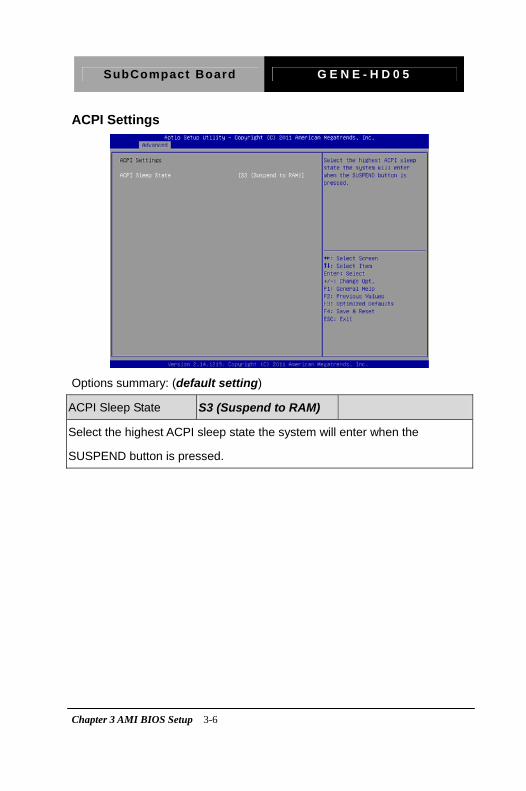
ACPI Settings
Options summary: (default setting)
ACPI Sleep State S3 (Suspend to RAM)
Select the highest ACPI sleep state the system will enter when the
SUSPEND button is pressed.
Chapter 3 AMI BIOS Setup 3-6

SubCompact Board G E N E - H D 0 5
CPU Configuration
Chapter 3 AMI BIOS Setup 3-7

SubCompact Board G E N E - H D 0 5
SATA Configuration
Options summary: (default setting)
Disabled OnChip SATA Channel
Enabled
En/Disable Serial ATA
ACHI OnChip SATA Type
Legacy IDE
Configure SATA controller operating as Legacy IDE/AHCI mode.
Chapter 3 AMI BIOS Setup 3-8
SubCompact Board G E N E - H D 0 5
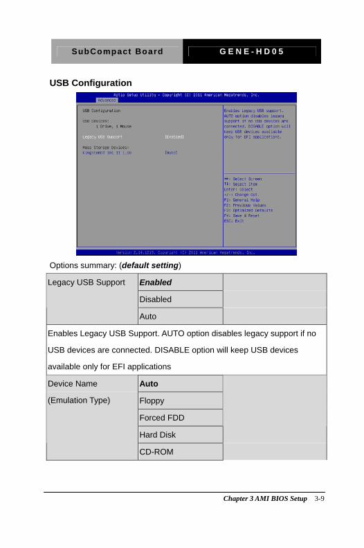
USB Configuration
Options summary: (default setting)
Enabled
Disabled
Legacy USB Support
Auto
Enables Legacy USB Support. AUTO option disables legacy support if no
USB devices are connected. DISABLE option will keep USB devices
available only for EFI applications
Auto
Floppy
Forced FDD
Hard Disk
Device Name
(Emulation Type)
CD-ROM
Chapter 3 AMI BIOS Setup 3-9
SubCompact Board G E N E - H D 0 5
If Auto. USB devices less than 530MB will be emulated as Floppy and
remaining as Floppy and remaining as hard drive. Forced FDD option can
be used to force a HDD formatted drive to boot as FDD(Ex. ZIP drive)
Chapter 3 AMI BIOS Setup 3-10
SubCompact Board G E N E - H D 0 5
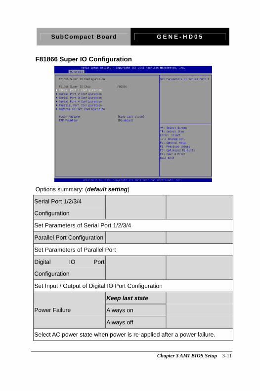
F81866 Super IO Configuration
Options summary: (default setting)
Serial Port 1/2/3/4
Configuration
Set Parameters of Serial Port 1/2/3/4
Parallel Port Configuration
Set Parameters of Parallel Port
Digital IO Port
Configuration
Set Input / Output of Digital IO Port Configuration
Keep last state
Always on Power Failure
Always off
Select AC power state when power is re-applied after a power failure.
Chapter 3 AMI BIOS Setup 3-11

SubCompact Board G E N E - H D 0 5
Disabled ERP Function
Enabled
ERP Function En/Disable
Chapter 3 AMI BIOS Setup 3-12
SubCompact Board G E N E - H D 0 5
Serial Port 1 Configuration
Options summary: (default setting)
Disabled Serial Port
Enabled
En/Disable specified serial port.
Auto
IO=3F8h; IRQ=4;
IO=3F8h; IRQ=3,4;
Change Settings
IO=2F8h; IRQ=3,4;
Select an optimal setting for Super IO device.
Chapter 3 AMI BIOS Setup 3-13
SubCompact Board G E N E - H D 0 5
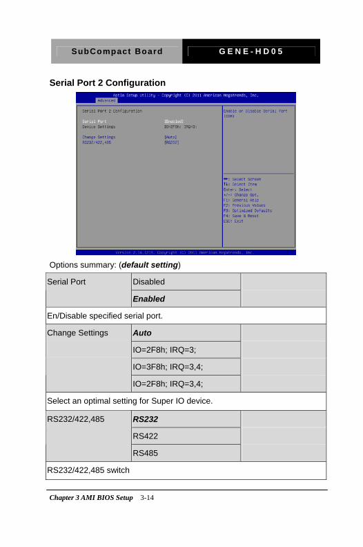
Serial Port 2 Configuration
Options summary: (default setting)
Disabled Serial Port
Enabled
En/Disable specified serial port.
Auto
IO=2F8h; IRQ=3;
IO=3F8h; IRQ=3,4;
Change Settings
IO=2F8h; IRQ=3,4;
Select an optimal setting for Super IO device.
RS232
RS422
RS232/422,485
RS485
RS232/422,485 switch
Chapter 3 AMI BIOS Setup 3-14

SubCompact Board G E N E - H D 0 5
Serial Port 3 Configuration
Options summary: (default setting)
Disabled Serial Port
Enabled
En/Disable specified serial port.
Auto
IO=3E8h; IRQ=11;
IO=3E8h; IRQ=11;
Change Settings
IO=2E8h; IRQ=11;
Select an optimal setting for Super IO device.
Chapter 3 AMI BIOS Setup 3-15
SubCompact Board G E N E - H D 0 5
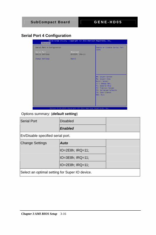
Serial Port 4 Configuration
Options summary: (default setting)
Disabled Serial Port
Enabled
En/Disable specified serial port.
Auto
IO=2E8h; IRQ=11;
IO=3E8h; IRQ=11;
Change Settings
IO=2E8h; IRQ=11;
Select an optimal setting for Super IO device.
Chapter 3 AMI BIOS Setup 3-16

SubCompact Board G E N E - H D 0 5
Parallel Port Configuration
Options summary: (default setting)
Disabled Parallel Port
Enabled
En/Disable specified parallel port.
Auto
IO=378h; IRQ=5;
IO=378h;
IRQ=5,6,7,10,11,12;
IO=278h;
IRQ=5,6,7,10,11,12;
Change Settings
IO=3BCh;
IRQ=5,6,7,10,11,12;
Select an optimal setting for Super IO device.
Chapter 3 AMI BIOS Setup 3-17

SubCompact Board G E N E - H D 0 5
STD Printer Mode
SPP Mode
EPP-1.9 and SPP Mode
EPP-1.7 and SPP Mode
ECP Mode
ECP and EPP 1.9 Mode
Device Mode
ECP and EPP 1.7 Mode
Change the Printer Port mode
Chapter 3 AMI BIOS Setup 3-18
SubCompact Board G E N E - H D 0 5
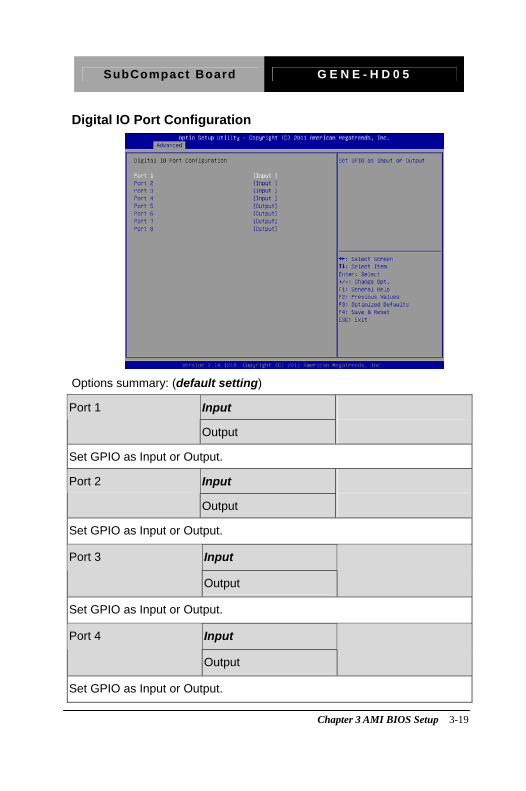
Digital IO Port Configuration
Options summary: (default setting)
Input Port 1
Output
Set GPIO as Input or Output.
Input Port 2
Output
Set GPIO as Input or Output.
Input Port 3
Output
Set GPIO as Input or Output.
Input Port 4
Output
Set GPIO as Input or Output.
Chapter 3 AMI BIOS Setup 3-19

SubCompact Board G E N E - H D 0 5
Input Port 5
Output
Set GPIO as Input or Output.
Input Port 6
Output
Set GPIO as Input or Output.
Input Port 7
Output
Set GPIO as Input or Output.
Input Port 8
Output
Set GPIO as Input or Output.
Keep last state
Always on
Power Failure
Always off
F81866 Power Failure
Disabled ERP Function
Enabled
ERP Function Enable / Disable
Chapter 3 AMI BIOS Setup 3-20
SubCompact Board G E N E - H D 0 5
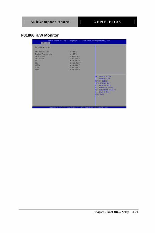
F81866 H/W Monitor
Chapter 3 AMI BIOS Setup 3-21

SubCompact Board G E N E - H D 0 5
Setup submenu: Chipset
Options summary: (default setting)
North Bridge
South Bridge Parameters
South Bridge
South Bridge Parameters
Chapter 3 AMI BIOS Setup 3-22

SubCompact Board G E N E - H D 0 5
North Bridge
Options summary: (default setting)
Graphics Configuration
Configure Graphics Settings.
Chapter 3 AMI BIOS Setup 3-23

SubCompact Board G E N E - H D 0 5
Graphics Configuration
Options summary: (default setting)
HDMI DP0 Output
Disabled
NB PCIE Connect Type (Display device)
LVDS DP1 Output
Disabled
NB PCIE Connect Type (Display device)
Chapter 3 AMI BIOS Setup 3-24
SubCompact Board G E N E - H D 0 5
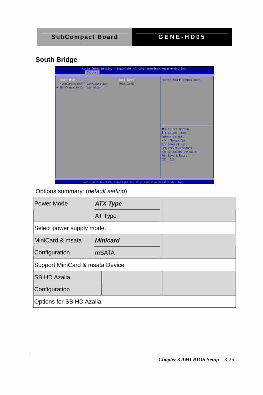
South Bridge
Options summary: (default setting)
ATX Type Power Mode
AT Type
Select power supply mode.
Minicard MiniCard & msata
Configuration mSATA
Support MiniCard & msata Device
SB HD Azalia
Configuration
Options for SB HD Azalia.
Chapter 3 AMI BIOS Setup 3-25
SubCompact Board G E N E - H D 0 5
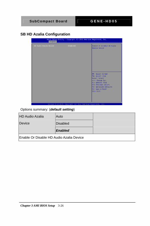
SB HD Azalia Configuration
Options summary: (default setting)
Auto
Disabled
HD Audio Azalia
Device
Enabled
Enable Or Disable HD Audio Azalia Device
Chapter 3 AMI BIOS Setup 3-26
SubCompact Board G E N E - H D 0 5
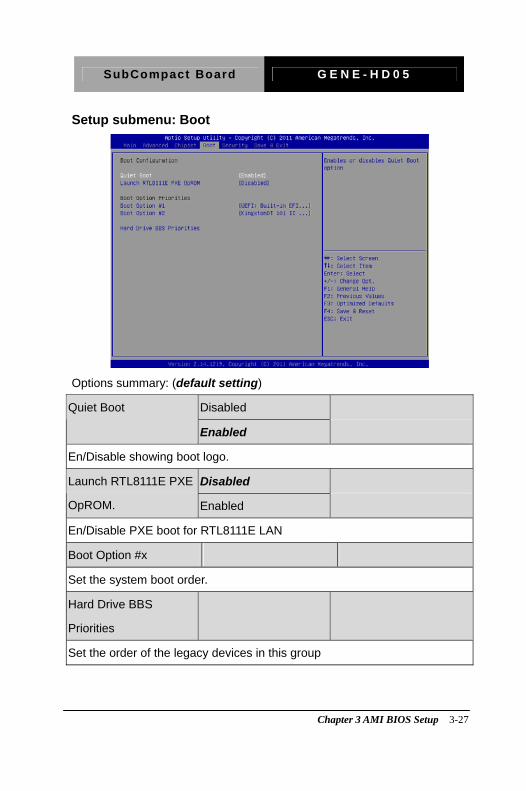
Setup submenu: Boot
Options summary: (default setting)
Disabled Quiet Boot
Enabled
En/Disable showing boot logo.
Disabled Launch RTL8111E PXE
OpROM. Enabled
En/Disable PXE boot for RTL8111E LAN
Boot Option #x
Set the system boot order.
Hard Drive BBS
Priorities
Set the order of the legacy devices in this group
Chapter 3 AMI BIOS Setup 3-27

SubCompact Board G E N E - H D 0 5
Setup submenu: Security
Options summary: (default setting)
Not set Administrator
Password/
User Password
You can install a Supervisor password, and if you install a supervisor password, you can then install a user password. A user password does not provide access to many of the features in the Setup utility.
Install the Password:
Press Enter on this item, a dialog box appears which lets you enter a password. You can enter no more than six letters or numbers. Press Enter after you have typed in the password. A second dialog box asks you to retype the password for confirmation. Press Enter after you have retyped it correctly. The password is required at boot time, or when the user enters the Setup utility.
Removing the Password:
Highlight this item and type in the current password. At the next dialog box press Enter to disable password protection.
Chapter 3 AMI BIOS Setup 3-28
SubCompact Board G E N E - H D 0 5
Chapter 3 AMI BIOS Setup 3-29
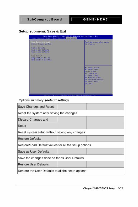
Setup submenu: Save & Exit
Options summary: (default setting)
Save Changes and Reset
Reset the system after saving the changes
Discard Changes and
Reset
Reset system setup without saving any changes
Restore Defaults
Restore/Load Default values for all the setup options.
Save as User Defaults
Save the changes done so far as User Defaults
Restore User Defaults
Restore the User Defaults to all the setup options
SubCompact Board G E N E - H D 0 5
Chapter 4 Driver Installation 4 - 1
Driver
Chapter
4Installation
SubCompact Board G E N E - H D 0 5
Chapter 4 Driver Installation 4 - 2
The GENE-HD05 comes with a DVD-ROM that contains all drivers and utilities that meet your needs.
Follow the sequence below to install the drivers:
Step 1 – Install Chipset Driver
Step 2 – Install LAN Driver
Step 3 – Install Audio Driver
Step 4 – Install AHCI Driver
Step 5 – Install Touch Driver
Step 6 – Install TPM Driver
Please read instructions below for further detailed installations.

SubCompact Board G E N E - H D 0 5
Chapter 4 Driver Installation 4 - 3
4.1 Installation:
Insert the GENE-HD05 DVD-ROM into the DVD-ROM Drive. And install the drivers from Step 1 to Step 6 in order.
Step 1 – Install Chipset Driver
1. Click on the STEP1-CHIPSET folder and select the OS folder your system is
2. Double click on the Setup.exe located in each OS folder
3. Follow the instructions that the window shows
4. The system will help you install the driver automatically
Step 2 – Install LAN Driver
1. Click on the STEP2-LAN folder and select the OS folder your system is
2. Double click on the setup.exe located in each OS folder
3. Follow the instructions that the window shows
4. The system will help you install the driver automatically
Step 3 – Install Audio Driver
1. Click on the STEP3-AUDIO folder and select the OS folder your system is
2. Double click on the Setup.exe located in each OS folder
3. Follow the instructions that the window shows
4. The system will help you install the driver automatically
SubCompact Board G E N E - H D 0 5
Chapter 4 Driver Installation 4 - 4
Step 4 – Install AHCI Driver
Please refer to the Appendix D AHCI Setting
Step 5 – Install Touch Driver
1. Click on the STEP5-TOUCH folder and double click on the Setup.exe
2. Follow the instructions that the window shows
3. The system will help you install the driver automatically
Step 6 – Install TPM Driver
1. Click on the STEP6-TPM folder and select the OS folder your system is
2. Double click on the Setup.exe file located in each OS folder
3. Follow the instructions that the window shows
4. The system will help you install the driver automatically

SubCompact Board G E N E - H D 0 5
Appendix A Programming the Watchdog Timer A-1
Programming the
Appendix
AWatchdog Timer
SubCompact Board G E N E - H D 0 5
Appendix A Programming the Watchdog Timer A-2
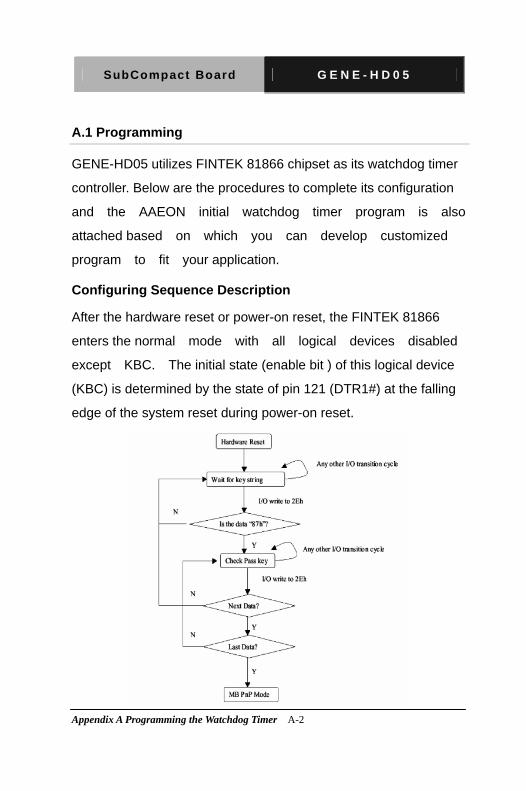
A.1 Programming
GENE-HD05 utilizes FINTEK 81866 chipset as its watchdog timer
controller. Below are the procedures to complete its configuration
and the AAEON initial watchdog timer program is also
attached based on which you can develop customized
program to fit your application.
Configuring Sequence Description
After the hardware reset or power-on reset, the FINTEK 81866
enters the normal mode with all logical devices disabled
except KBC. The initial state (enable bit ) of this logical device
(KBC) is determined by the state of pin 121 (DTR1#) at the falling
edge of the system reset during power-on reset.

SubCompact Board G E N E - H D 0 5
Appendix A Programming the Watchdog Timer A-3
There are three steps to complete the configuration setup: (1) Enter
the MB PnP Mode; (2) Modify the data of configuration registers; (3)
Exit the MB PnP Mode. Undesired result may occur if the MB PnP
Mode is not exited normally.
(1) Enter the MB PnP Mode
To enter the MB PnP Mode, four special I/O write operations are to
be performed during Wait for Key state. To ensure the initial state of
the key-check logic, it is necessary to perform four write opera-tions
to the Special Address port (2EH). Two different enter keys are
provided to select configuration ports (2Eh/2Fh) of the next step.
(2) Modify the Data of the Registers
All configuration registers can be accessed after entering the MB
PnP Mode. Before accessing a selected register, the content of
Index 07h must be changed to the LDN to which the register
belongs, except some Global registers.
(3) Exit the MB PnP Mode
Write exit key 0xAA to the index port.

SubCompact Board G E N E - H D 0 5
Appendix A Programming the Watchdog Timer A-4
Watch Dog Timer 1, 2, 3 Control Register (Index=F5h,F6h,FAh
Default=00h)

SubCompact Board G E N E - H D 0 5
Appendix A Programming the Watchdog Timer A-5
A.2 F81866 Watchdog Timer Initial Program
Main(){
aaeonSuperIOOpen();
aaeonWdtSetCountMode(BOOL bMinute); // Set wdt count mode
aaeonWdtSetTimeoutCount(BYTE tTimeout); // Set wdt timer
aaeonWdtSetEnable(BOOL bEnable); // Enable wdt
aaeonSuperIOClose();
}
Void aaeonSuperIOOpen(){ // Config F81866 Entry key
aaeonioWritePortByte(F81866_INDEX, 0x87);
aaeonioWritePortByte(F81866_INDEX, 0x87);
}
Void aaeonWdtSetCountMode(BOOL bMinute){
BYTE WDT_CONTROL = f81866ReadByte(F81866_WDT_CONTROL_REG);
if(bMinute)
f81866WriteByte(F81866_WDT_CONTROL_REG, WDT_CONTROL | 0x08);
else
f81866WriteByte(F81866_WDT_CONTROL_REG, WDT_CONTROL & 0xF7);
}

SubCompact Board G E N E - H D 0 5
Appendix A Programming the Watchdog Timer A-6
Void aaeonWdtSetTimeoutCount(BYTE tTimeout){
f81866SetLdn(0x07);
f81866WriteByte(F81866_WDT_TIME_REG, tTimeout);
}
Void aaeonWdtSetEnable(BOOL bEnable){
f81866SetLdn(0x07);
if(bEnable){
f81866WriteByte(0x30, 0x01);
WDT_BASE_ADDR =
(f81866ReadByte(F81866_WDT_BASEADDR_REG_MSB) << 8)
| f81866ReadByte(F81866_WDT_BASEADDR_REG_LSB);
WDT_STATUS = f81866ReadByte(F81866_WDT_CONTROL_REG);
f81866WriteByte(F81866_WDT_CONTROL_REG, WDT_STATUS | 0x20);
WDT_STATUS = f81866ReadByte(F81866_WDT_PME_REG);
f81866WriteByte(F81866_WDT_PME_REG, WDT_STATUS | 0x01);
}else{
f81866WriteByte(0x30, 0x00);
WDT_BASE_ADDR = 0;
WDT_STATUS = f81866ReadByte(F81866_WDT_CONTROL_REG);
f81866WriteByte(F81866_WDT_CONTROL_REG, WDT_STATUS & 0xDF);
WDT_STATUS = f81866ReadByte(F81866_WDT_PME_REG);
f81866WriteByte(F81866_WDT_PME_REG, WDT_STATUS & 0xFE);
}
}

SubCompact Board G E N E - H D 0 5
Appendix A Programming the Watchdog Timer A-7
Void aaeonSuperIOClose(){
aaeonioWritePortByte(F81866_INDEX, 0xaa);
}
SubCompact Board G E N E - H D 0 5
Appendix B I/O Information B-1
I/O Information
Appendix
B
SubCompact Board G E N E - H D 0 5
Appendix B I/O Information B-2
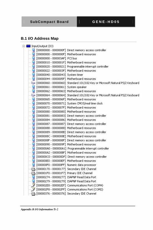
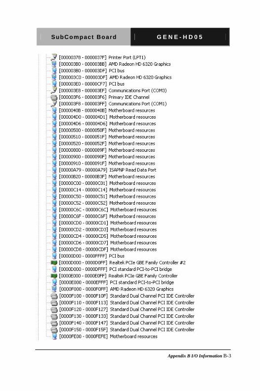
B.1 I/O Address Map
SubCompact Board G E N E - H D 0 5
Appendix B I/O Information B-3
SubCompact Board G E N E - H D 0 5
Appendix B I/O Information B-4
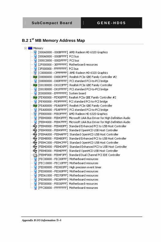
B.2 1st MB Memory Address Map
SubCompact Board G E N E - H D 0 5
Appendix B I/O Information B-5
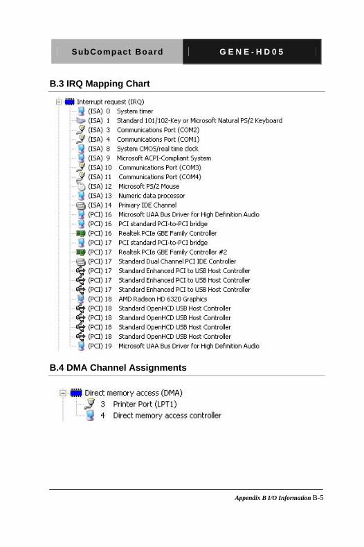
B.3 IRQ Mapping Chart
B.4 DMA Channel Assignments

SubCompact Board G E N E - H D 0 5
Appendix C Mating Connector C - 1
Mating Connector
Appendix
C
SubCompact Board G E N E - H D 0 5
Appendix C Mating Connector C - 2
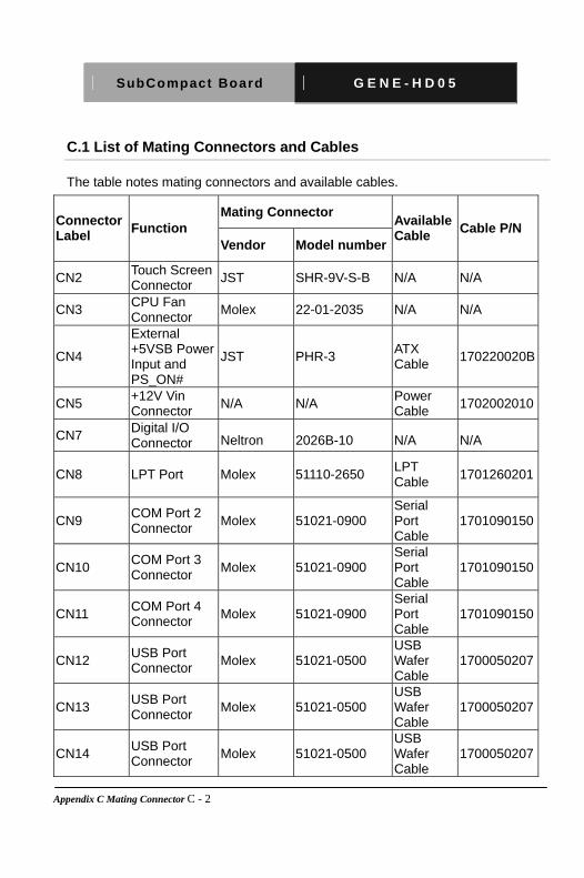
C.1 List of Mating Connectors and Cables
The table notes mating connectors and available cables.
Mating Connector Connector Label
Function Vendor Model number
Available Cable
Cable P/N
CN2 Touch Screen Connector
JST SHR-9V-S-B N/A N/A
CN3 CPU Fan Connector
Molex 22-01-2035 N/A N/A
CN4
External +5VSB Power Input and PS_ON#
JST PHR-3 ATX Cable
170220020B
CN5 +12V Vin Connector
N/A N/A Power Cable
1702002010
CN7 Digital I/O Connector Neltron
2026B-10
N/A N/A
CN8 LPT Port Molex 51110-2650 LPT Cable
1701260201
CN9 COM Port 2 Connector
Molex 51021-0900 Serial Port Cable
1701090150
CN10 COM Port 3 Connector
Molex 51021-0900 Serial Port Cable
1701090150
CN11 COM Port 4 Connector
Molex 51021-0900 Serial Port Cable
1701090150
CN12 USB Port Connector
Molex 51021-0500 USB Wafer Cable
1700050207
CN13 USB Port Connector
Molex 51021-0500 USB Wafer Cable
1700050207
CN14 USB Port Connector
Molex 51021-0500 USB Wafer Cable
1700050207

SubCompact Board G E N E - H D 0 5
Appendix C Mating Connector C - 3
CN15 USB Port Connector
Molex 51021-0500 USB Wafer Cable
1700050207
CN16 USB Port Connector
Molex 51021-0500 USB Wafer Cable
1700050207
CN17 USB Port Connector
Molex 51021-0500 USB Wafer Cable
1700050207
CN18 Audio Connector
Molex 51021-1000 Audio Cable
1709100254
CN21 +5Vout Connector
JST PHR-2 2 Pins For HDD Power
1702150155
CN22 LVDS Inverter Connector
JST PHR-5 N/A N/A
CN23 LVDS Connector
HIROSE DF13-30DS-1.25C
N/A N/A
CN29 P/S2 KB/MS Connector
JST PHDR-06VS P/S2 KB/MS Cable
1700060152
BATA1 External RTC Connector
Molex 51021-0200 Battery Cable
175011901C
SubCompact Board G E N E - H D 0 5
Appendix D AHCI Setting D-1
AHCI Setting
A ppendix
D

SubCompact Board G E N E - H D 0 5
Appendix D AHCI Setting D-2
D.1 Setting AHCI
OS installation to setup AHCI Mode.
Step 1: Copy the files below from “Driver DVD -> STEP4 -
AHCI\WinXP\SB8xx_RAID_XP_3.2.1540.92” to Disk
Step 2: Connect the USB Floppy to the board (The board on the photo is
just for reference)
SubCompact Board G E N E - H D 0 5
Appendix D AHCI Setting D-3
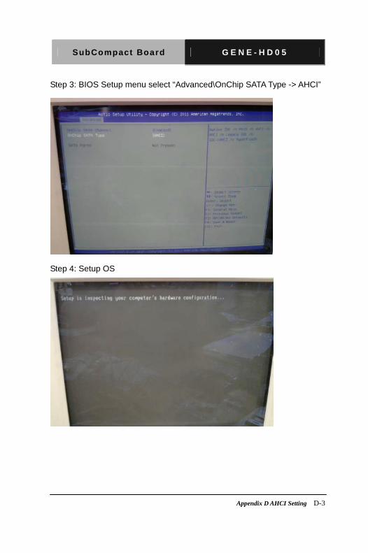
Step 3: BIOS Setup menu select “Advanced\OnChip SATA Type -> AHCI”
Step 4: Setup OS

SubCompact Board G E N E - H D 0 5
Appendix D AHCI Setting D-4
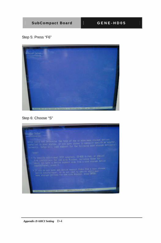
Step 5: Press “F6”
Step 6: Choose “S”

SubCompact Board G E N E - H D 0 5
Appendix D AHCI Setting D-5
Step 7: Choose “AMD® A50M”
Step 8: It will show the model number you select and then press “ENTER”
Step 9: Setup is loading files

SubCompact Board G E N E - H D 0 5
Appendix D AHCI Setting D-1
AHCI Setting
A ppendix
D

SubCompact Board G E N E - H D 0 5
Appendix D AHCI Setting D-2
D.1 Setting AHCI
OS installation to setup AHCI Mode.
Step 1: Copy the files below from “Driver DVD -> STEP4 -
AHCI\WinXP\SB8xx_RAID_XP_3.2.1540.92” to Disk
Step 2: Connect the USB Floppy to the board (The board on the photo is
just for reference)

SubCompact Board G E N E - H D 0 5
Appendix D AHCI Setting D-3
Step 3: BIOS Setup menu select “Advanced\OnChip SATA Type -> AHCI”
Step 4: Setup OS
SubCompact Board G E N E - H D 0 5
Appendix D AHCI Setting D-4
Step 5: Press “F6”
Step 6: Choose “S”

SubCompact Board G E N E - H D 0 5
Appendix D AHCI Setting D-5
Step 7: Choose “AMD® A50M”
Step 8: It will show the model number you select and then press “ENTER”
Step 9: Setup is loading files

SubCompact Board G E N E - H D 0 5
Appendix E Electrical Specifications for I/O Ports E-1
Electrical Specifications
Appendix
Efor I/O Ports

SubCompact Board G E N E - H D 0 5
Appendix E Electrical Specifications for I/O Ports E-2
E.1 Electrical Specifications for I/O Ports
I/O Reference Signal Name Rate Output
LVDS Inverter / Backlight Connector
CN22 VDD +5V/2A or +12V/2A
LPC Port CN1 +3.3VCC +3.3V/0.5A
CPU FAN CN3 VDD +12V/0.5A
Digital IO Port CN7 D0~D7 +3.3V/(Open drain)
COM Port 2 CN9 +5V/+12V +5V/1A or +12V/0.5A
USB 2.0 Ports 7 CN12 +5V
USB 2.0 Ports 8 CN13 +5V +5V/0.5A (per channel)
USB 2.0 Ports 5 CN14 +5V
USB 2.0 Ports 6 CN15 +5V
USB 2.0 Ports 3 CN16 +5V
USB 2.0 Ports 4 CN17 +5V
Audio I/O Port CN18 +5V +5V/1A
+5V Output for SATA HDD
CN21 +5V +5V/1A
LVDS Port CN23 VCC +3.3V/1A or +5V/1A
USB Ports 1 and 2
CN27 VCC +5V/1A (per channel)
PS/2 Keyboard/Mouse Combo Port
CN29 +5V +5V/1A
VGA Port CN30 +5V +5V/1A (reserved) +5V/0.5A
CFast Slot CFDA1 +3.3V +3.3V/0.5A
SubCompact Board G E N E - H D 0 5
Appendix E Electrical Specifications for I/O Ports E-3
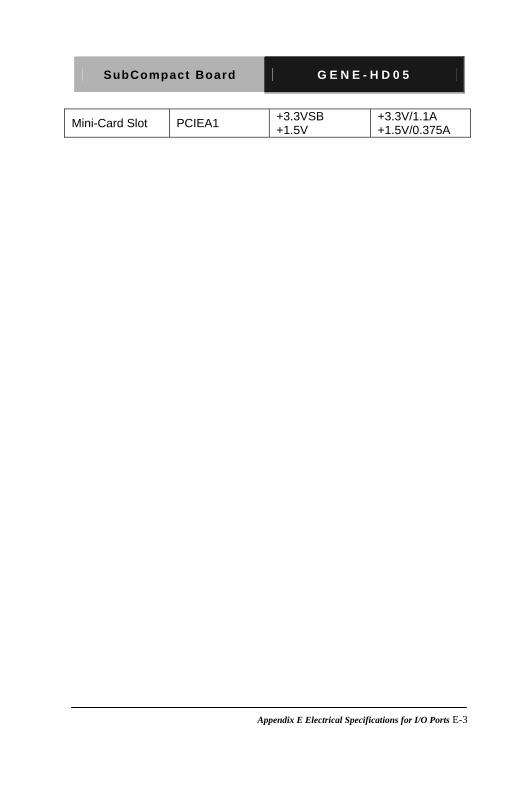
Mini-Card Slot PCIEA1 +3.3VSB +1.5V
+3.3V/1.1A +1.5V/0.375A