SU PPLEMENTAR Y INFORMATION - Nature. SUPPLEMENTARY DISCUSSION 1. Fabrication of Probes The steps...
27
A. SUPPLEMENTARY FIGURES AND LEGENDS Figure S1. Schematics of the modulation scheme used in this work. (a) The modulated periodic voltage signal V M (t) applied to AMJs. (b) The resulting modulated current I M (t). (c) The modulated voltage output ΔV M, TC (t) from the integrated thermocouple, which is related to the time-averaged temperature rise ΔT TC, Avg by the relationship shown at the bottom of the figure. Figure S2. The conductance traces (inset) of Au-Au atomic junctions are shown along with a histogram obtained from 500 such traces. The histogram features a prominent peak at G 0 showing the most probable conductance of Au-Au atomic junctions. V M (t) Time I M (t) ΔV M,TC (t) Δt T Time Time ΔT TC, Avg (+V M )=3[AR-AG]/[2TxSTC], ΔT TC, Avg (-V M )=3[AB-AG]/[2TxSTC] AR, AG, AB are the sum of the areas of red, green, and blue rectangles respectively -T V M I M ~ ~ T P =(1/12.25Hz) ~ ~ a b c Counts (arb.) Conductance (G 0 ) 1 2 3 4 Displacement (nm) 0 0.4 0.8 1.2 1.6 0 1 2 3 4 Conductance (G 0 ) SUPPLEMENTARY INFORMATION doi:10.1038/nature12183 WWW.NATURE.COM/NATURE | 1
-
Upload
trinhxuyen -
Category
Documents
-
view
216 -
download
0
Transcript of SU PPLEMENTAR Y INFORMATION - Nature. SUPPLEMENTARY DISCUSSION 1. Fabrication of Probes The steps...

A. SUPPLEMENTARY FIGURES AND LEGENDS
Figure S1. Schematics of the modulation scheme used in this work. (a) The modulated periodic voltage signal VM(t) applied to AMJs. (b) The resulting modulated current IM(t). (c) The modulated voltage output ΔVM, TC(t) from the integrated thermocouple, which is related to the time-averaged temperature rise ΔTTC, Avg by the relationship shown at the bottom of the figure.
Figure S2. The conductance traces (inset) of Au-Au atomic junctions are shown along with a histogram obtained from 500 such traces. The histogram features a prominent peak at G0 showing the most probable conductance of Au-Au atomic junctions.
VM(t)Time
IM(t)
!VM,TC(t)
!t
T
Time
Time
!TTC, Avg(+VM)=3[AR-AG]/[2TxSTC], !TTC, Avg(-VM)=3[AB-AG]/[2TxSTC]AR, AG, AB are the sum of the areas of red, green, and blue rectangles respectively
-T
VM
IM
~~
TP =(1/12.25Hz)
~ ~
a
b
c
Coun
ts (a
rb.)
Conductance (G0)1 2 3 4
Displacement (nm)0 0.4 0.8 1.2 1.6
0
1
2
3
4
Cond
ucta
nce
(G0)
SUPPLEMENTARY INFORMATIONdoi:10.1038/nature12183
WWW.NATURE.COM/NATURE | 1

B. SUPPLEMENTARY DISCUSSION
1. Fabrication of Probes
The steps involved in the fabrication of the custom-fabricated NTISTPs are shown in Fig. S3 and are described next. (Step 1) fabrication begins by depositing a ~500 nm thick low-stress low-pressure chemical vapor deposition (LPCVD) SiNx on both sides of a silicon wafer. (Step 2) An 8 µm thick layer of low temperature silicon oxide (LTO) is deposited on both sides of the wafer and is annealed at 1000°C for 1 hour to reduce the residual stress of SiNx and LTO layers (this LTO layer is eventually patterned to create the probe tip). Subsequently, a 100 nm thick chromium (Cr) cap is lithographically patterned by Cr etching: this Cr cap facilitates the creation of the probe tip from the LTO layer by etching. (Step 3) The LTO probe tip is fabricated by etching in buffered HF (HF : NH4F = 1:5), which takes ~100 minutes. In order to obtain a sharp tip the etching status of the tip is monitored, at 10 minute intervals, by using an optical microscope. (Step 4) After fabrication of a sharp LTO tip, a gold (Au) line (Cr/Au: 5/90 nm) is lithographically defined by sputtering and Au etching. This Au line is the first metal layer of the NTISTP.
Figure S3. Fabrication of the NTISTPs. (a) The fabrication steps involved in the creation of NTISTPs are shown. (b & c) Scanning electron microscope (SEM) images of fabricated probes. The false coloring identifies the metal layers (Au, Cr) that comprise the thermocouple (TC) and the outermost Au metal layer that is used to create atomic-scale junctions. (d) SEM image of the tip of a fabricated NTISTP.
Subsequently, a 70 nm thick layer of plasma enhanced chemical vapor deposition (PECVD) SiNx is deposited to insulate the two metal layers (Au which is deposited in step 4 and Cr that is deposited in step 6) everywhere except at the tip of the probe: these metal layers comprise of the
Step 1
Step 2
Step 3
Step 4
Step 5
Step 6
SiLPCVD SiNxLTO
CrAu
PECVD SiNx1827 PR
Step 7
Step 8
a b
c
d
500 µm
Cr (TC)
Au (TC)
Au
Au (TC)
Cr (TC)
Au
30 µm
Tip
Thick Si cantilever
Probe body
Outer Au + Au-Cr TC
2 µm
SUPPLEMENTARY INFORMATIONRESEARCHdoi:10.1038/nature12183
WWW.NATURE.COM/NATURE | 2

nanoscale thermocouple. (Step 5) In order to create a nanoscale thermocouple junction on the apex of the probe tip, a 6 µm thick Shipley Microposit S1827 photoresist is deposited on the probe. The photoresist and PECVD SiNx is slowly plasma etched until a very small portion of the Au layer is exposed. (Step 6) A Cr line (~90 nm thick) is deposited by sputtering and is etched after lithography. This Cr line is the second metal layer of the NTISTP and contacts the Au layer only at the apex of the tip. (Step 7) 70 nm thick PECVD SiNx is deposited to insulate the Cr-Au thermocouple junction from the third metal layer. Finally, a Au layer (Cr/Au: 5/90 nm) is lithographically defined by sputtering and Au etching. This Au layer represents the outermost electrode of the probe and is critical for creating Au-Au atomic junctions and Au-single molecule-Au junctions. (Step 8) In the last step, the NTISTPs are released by deep reactive ion etching (DRIE). Figs. S3b, c, and d show scanning electron micrograph images of a fabricated NTISTP. We note that the fabricated probes are designed to be much stiffer than traditional scanning thermal microscopy probes31 so as to enable stable trapping of AMJs. 2. Landauer Approach: General Considerations As explained in the main text, within the Landauer approach to coherent transport, the power dissipation (heat dissipation per unit time) in the electrodes of atomic-scale junctions is given by eq. (1). From those expressions, it is straightforward to draw some general conclusions about the symmetry of the dissipated heat (with respect to both the electrodes and the bias polarity). The first question that we want to address concerns the conditions under which the power is equally dissipated in both electrodes [QP (V ) =QS (V )]. To answer this question, we assume (without loss of generality) that all the energies are measured with respect to the equilibrium chemical potential, which we set to zero ( µ = 0). Moreover, we assume a symmetric biasing scheme: µP = eV / 2 and µS = −eV / 2 . Obviously, the conclusions drawn below are independent of this choice since the measurable quantities must be gauge-invariant, i.e. independent of the biasing scheme. With this choice, the power dissipated in the probe electrode is given by:
QP (V ) =2h
(eV / 2 − E)τ (E,V )[ f (E − eV / 2)− f (E + eV / 2)]dE.−∞
∞
∫ (S1)
Making use of the change of variable E→−E, the previous expression becomes:
QP (V ) =2h
(E + eV / 2)τ (−E,V )[ f (E − eV / 2)− f (E + eV / 2)]dE.−∞
∞
∫ (S2)
Here, we have used the relation f (−x) = 1− f (x). Equation (S2) has to be compared with the corresponding expression for the power dissipated in the substrate,
QS (V ) =2h
(E + eV / 2)τ (E,V )[ f (E − eV / 2)− f (E + eV / 2)]dE.−∞
∞
∫ (S3)
Thus, we conclude that QP (V ) =QS (V ) if τ (E,V ) = τ (−E,V ), i.e. if the transmission function has inversion symmetry with respect to the chemical potential, or in other words, if the transport
SUPPLEMENTARY INFORMATIONRESEARCHdoi:10.1038/nature12183
WWW.NATURE.COM/NATURE | 3

is electron-hole symmetric. This in turn implies a trivial linear relation between QP (V ) and the total power dissipated in the junction QTotal (V ) = I ×V , namely QP (V ) =QTotal (V ) / 2 . Notice that this relation is independent of the bias dependence of these two powers. Obviously, if the transmission is energy-independent in the transport window, then the power dissipation is the same in both electrodes. This explains the observed heat dissipation properties of Au junctions. Another central question in our work is related to the asymmetry of the power dissipated in an electrode with respect to the bias polarity. Following a similar line of reasoning as above, one can show that QP (V ) =QP (−V ) if τ (E,V ) = τ (−E,−V ) is satisfied. This means, in particular, that if the transmission does not depend significantly on the bias voltage, the power dissipated in an electrode is symmetric with respect to the inversion of the bias as long as there is electron-hole symmetry. Obviously, if the transmission is independent of both the energy and the bias, then the heating is symmetric. This is what occurs in the Au atomic junctions for not too high voltages. Finally, let us say that, analogously, one can show that the relation QP (V ) =QS (−V ) is satisfied if τ (E,V ) = τ (E,−V ). Furthermore, this relation leads naturally to the following one: QP (V )+QP (−V ) =QP (V )+QS (V ) =QTotal = I ×V . This means that if the transmission is symmetric with respect to the inversion of the bias voltage, then the average dissipated heat in an electrode (for positive and negative bias) is equal to half of the total power dissipated in the junction. This is in fact the relation that we have found experimentally in all the AMJs analyzed in this work. This is indeed reasonable since all our AMJs are approximately left-right symmetric and therefore, the voltage profile is expected to be symmetric with respect to the center of the junction. This implies, in turn, that the relation τ (E,V ) = τ (E,−V )will hold in all our AMJs32. From the general considerations above, it is clear that in order to have a heating asymmetry of the type QP (V ) ≠QP (−V ), one needs a certain degree of the electron-hole asymmetry. This can be seen explicitly by expanding QP (V ) in eq. (S1) to first order in the bias voltage, which gives:
QP (V ) =2eVh
Eτ (E,V = 0) ∂ f (E,T )∂E
dE−∞
∞
∫ = GTSV . (S4)
Here, G is the low bias electrical conductance of the junction, T is absolute temperature, and S is the thermopower or Seebeck coefficient of the junction. In the same way, one can show thatQS (V ) = −GTSV . These expressions lead immediately to the first order terms in eq. (2) in the main text. Moreover, we can perform a Taylor’s expansion in the previous equation to obtain the leading contribution at low temperatures, which reads:
QP (V ) = − 2eh
⎛⎝⎜
⎞⎠⎟π 2
3(kBT )
2 ′τ (EF ,V = 0)V , (S5)
where ′τ (EF ,V = 0) is the energy derivative of the zero-bias transmission at the Fermi energy. Thus, we see that the slope of the transmission function determines, to first order in the bias voltage, both the magnitude and the sign of the heating asymmetry.
SUPPLEMENTARY INFORMATIONRESEARCHdoi:10.1038/nature12183
WWW.NATURE.COM/NATURE | 4
Our experimental results show that the temperature rise in the probe, and in turn the power dissipated there, is roughly proportional to the total power dissipated in the junction QTotal = I ×V . This can be understood by expanding QP (V ) in eq. (S1) up to second order in the bias voltage. Ignoring the bias dependence of the transmission function, the second-order term is given by (1 / 2)GV 2, which is equal to half of the total power in the linear regime. We note that this is also the second order term for QS (V ) , which implies that there is no quadratic term in the bias in eq. (2). This second-order term dominates over the linear one as long as V > 2T S . Thus for instance, if we assume room temperature (T = 300 K) and a typical value of |S| = 10 µV/K, then the second-order term dominates the contribution to the heating for voltages |V| > 6 mV. This explains why the local heating is roughly proportional to the total power dissipated in the junction, at least in a certain voltage range. Of course, at sufficiently high bias, higher order terms in the voltage expansion (beyond the quadratic one) may give a significant contribution to the local heating. In particular, odd terms, like the cubic one, can then play an important role in the heating asymmetry. We can estimate the voltage at which these higher order terms become relevant by expanding QP to third order in the bias. Ignoring the voltage dependence of the transmission, one can show that the cubic term is given by −(1 /12)eG0 ′τ (EF ,V = 0)V 3. Notice first that this term is also determined by the energy derivative of the transmission at the Fermi energy, in the spirit of eq. (S5). Comparing this contribution with the linear one of eq. (S5), we see that the third order term would dominate the contribution to the heating asymmetry at room temperature for biases above approximately 0.2 V. Thus, contributions of non-linear terms to the heating asymmetry of our molecular junctions are indeed expected to show up in the voltage range explored in our experiments, as it indeed occurs (see insets of Fig. 2b and 3b). We note that all these contributions are completely taken into account by the exact expressions for the power dissipated in the electrodes (eq. 1 in the manuscript), as we have done in all the calculations presented in the manuscript and in the next section. 3. Ab Initio Calculations: Atomic and Molecular Junctions The goal of this section is to describe the procedure that we have followed in the ab initio calculations of the transmission curves of the different systems discussed in the main text: gold atomic junctions and single-molecule junctions. We have employed our transport method based on density functional theory (DFT), which has been described in great detail24. This method is built upon the quantum-chemistry code TURBOMOLE33. The first step in this method is the description of the electronic structure of the junctions within DFT. In all the calculations described here we have used the BP86 exchange-correlation functional34 and the Gaussian basis set def-SVP35. The total energies were converged to a precision of better than 10-6 atomic units, and structure optimizations were carried out until the maximum norm of the Cartesian gradient fell below 10-4 atomic units. The final step in our method is the transformation of the information on the electronic structure of the junctions obtained with DFT into the elastic transmission of the junctions. This is done with the help of non-equilibrium Green’s function techniques, as explained in detail in our past work24. In what follows, we shall separately address the analysis of gold atomic junctions and single-molecule junctions.
SUPPLEMENTARY INFORMATIONRESEARCHdoi:10.1038/nature12183
WWW.NATURE.COM/NATURE | 5
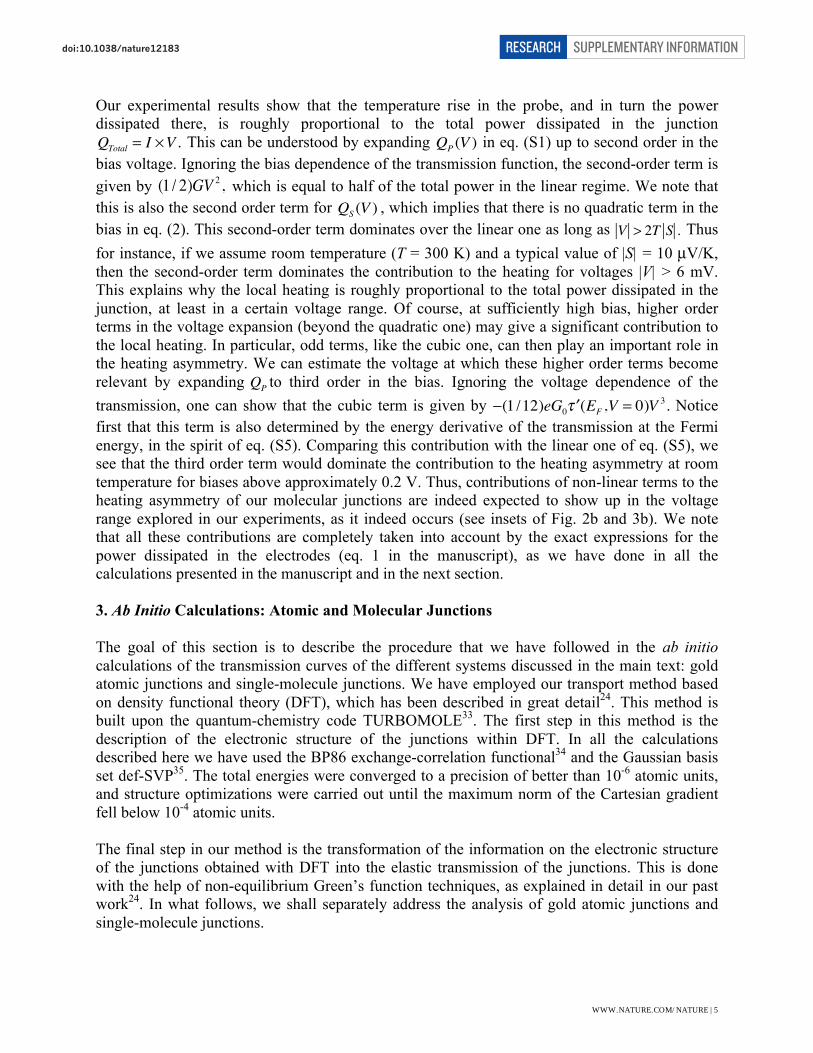
3.1 Gold Atomic Junctions The analysis of the transmission curves of gold atomic junctions was already reported by some of us36. Thus, we just present a brief description of the transmission calculations and focus on the consequences for the local heating in these junctions. To study a Au atomic junction we first define an ideal geometry like the example shown in Fig. S4a, which corresponds to the junction shown in the inset-i of Fig. 4b in the main text. It consists of two pyramids grown along the 100 direction of an fcc lattice and facing each other such that they form an atom dimer in the
narrowest part of the junction. We relax the positions of the atoms located both in the dimer and in the two neighboring layers (consisting of four atoms each). The other atoms in the junction are kept fixed, and the lattice constant is set to 0.408 nm, the experimental value for gold. We present in Fig. S4b the zero-bias transmission as a function of the energy for the junction shown in panel a. The corresponding results for the heating in the probe electrode as a function of the total power dissipated in the junction are shown in Fig. S4c (for positive and negative bias). The heating has been calculated using eq. (S1) and the zero-bias transmission function, i.e. we have assumed that the transmission is independent of the bias, which is justified in view of the linearity of the experimental I-V curves (see inset-ii of Fig. 4b). This assumption has also been used, together with the Landauer formula, to compute the total power. As one can see, the power dissipated in the probe electrode is symmetric with respect to the inversion of the bias, which is in perfect agreement with our experimental results (see Fig. 4a). This is a consequence of the weak energy dependence of the transmission in the transport window and of the negligible slope at the Fermi energy (i.e. the thermopower vanishes).
Figure S4. Ab initio calculations of the transmission and heat dissipation in gold atomic junctions. (a) The model of a Au atomic junction with a conductance close to 1G0. (b) The transmission (as computed from our DFT approach) as a function of the energy for the atomic junction. (c) The computed results for the heating in the probe electrode for positive and negative bias voltages as a function of the total power dissipated in the junction. 3.2 Single-Molecule Junctions We now describe our DFT-based calculations of the transmission and heating in Au-1,4-benzenediisonitrile-Au (Au-BDNC-Au) and Au-1,4-benzenediamine-Au (Au-BDA-Au) junctions. In this case, we first relax the isolated molecules. Then, we construct the single-
E-EF (eV)0
0.5
1
1.5
2
Tran
smis
sion
0
0.2
0.4
0.6
negative biaspositive biasAu-Au atomic junction
a
-2 -1 0 1 2QTotal (µW)
QP
(µW
)
0.6 10.80 0.2 0.4
b c
SUPPLEMENTARY INFORMATIONRESEARCHdoi:10.1038/nature12183
WWW.NATURE.COM/NATURE | 6

molecule junctions by placing the relaxed molecules in between two gold clusters with 20 (or 19) atoms. Subsequently, we perform a new geometry optimization by relaxing the positions of all the atoms in the molecule as well as the four (or three) outermost gold atoms on each side, while the other gold atoms are kept frozen. Afterwards, the size of the gold cluster is increased to about 63 atoms on each side in order to describe correctly both the metal-molecule charge transfer and the energy level alignment. Finally, the central region, consisting of the molecule and one or two Au layers is coupled to ideal gold surfaces, which serve as infinite electrodes and are treated consistently with the same functional and basis set within DFT24. Figure S5. Ab initio results for the transmission and local heat dissipation in Au-BDNC-Au junctions. (a-b) The two atop Au-BDNC-Au junction geometries investigated here. (c-d) The computed zero-bias transmission as a function of the energy for the two geometries. For clarity, the position of the Fermi level has been indicated with vertical lines. (e-f) The corresponding results for the heating in the probe electrode, for positive and negative biases, as a function of the total power dissipated in the Au-BDNC-Au junction. 3.2.1 Au-BDNC-Au Junctions: First of all, we have studied the most probable geometries of the Au-BDNC-Au junctions and we have found that the isonitrile group binds preferentially to low-coordinated gold atoms in atop positions. This is in agreement with previous studies of adsorption of isocyanides on gold surfaces37. Two representative examples of the atop geometries found in our analysis are shown in the Figs. S5a and b. Notice that in both cases the C atom is directly bound to a single Au atom and the main difference between the two geometries lies in the shape of the electrodes. The results for the zero-bias transmission as a function of energy for these two junctions are shown in Figs. S5c and d. In both cases the conductance, determined by the transmission at the Fermi energy, is dominated by the LUMO.
-3 -2 -1 0 1 2 30.001
0.01
0.1
1
Tran
smis
sion
-3 -2 -1 0 1 2 30.001
0.01
0.1
1
Tran
smis
sion
0 0.1 0.2 0.3 0.40
0.05
0.1
0.15
0.2negative biaspositive bias
0 0.1 0.2 0.3 0.40
0.05
0.1
0.15
0.2negative biaspositive bias
E-EF (eV)E-EF (eV)
QP
(µW
)
QP
(µW
)
QTotal (µW) QTotal (µW)
a b
c d
e f
SUPPLEMENTARY INFORMATIONRESEARCHdoi:10.1038/nature12183
WWW.NATURE.COM/NATURE | 7

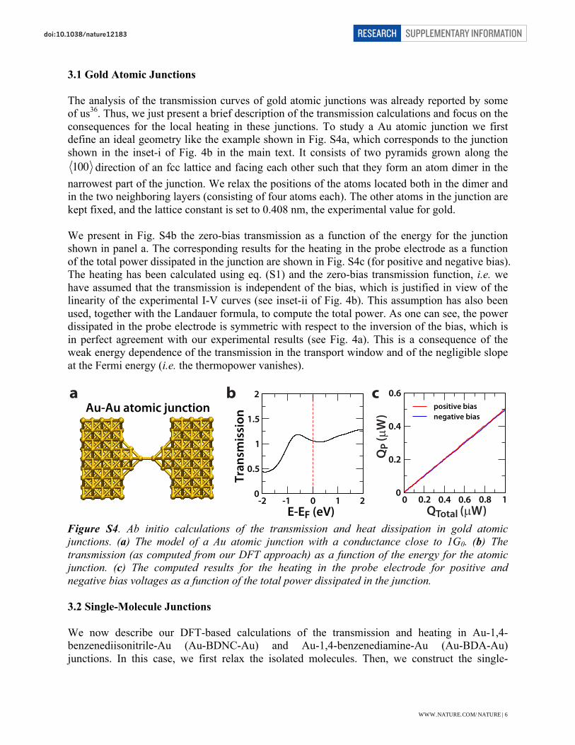
This is in qualitative agreement with previous results25,38. The conductance values in these two examples are 0.048G0 (left junction) and 0.14G0 (right junction). These values are clearly higher than the value of 0.002G0 found in our experiments. We attribute this discrepancy to the intrinsic deficiencies of the existent DFT functionals that tend to underestimate the HOMO-LUMO gap. On the other hand, making use of eq. (S1), we have also computed the power dissipated in the probe electrode for these two junctions as a function of the total power dissipated in the junction and the results for positive and negative bias are shown in Figs. S5e and f. In these calculations we have approximated the transmission curves by the zero-bias functions shown in Fig. S5c and d. This approximation is justified by the fact that the highest bias explored in our experiments is still quite low as compared to the HOMO-LUMO of the molecules. Moreover, in our relatively weakly-coupled and symmetric molecular junctions the voltage is expected to drop mainly at the metal-molecule interfaces. This means that the relevant orbitals in the molecule are not significantly shifted by the bias and thus, the transmission is expected not to vary appreciably with the voltage, see for instance Ref. 32. As one can see in Figs. S5e and f, the heating in the probe is clearly asymmetric and is larger for negative voltages as a result of the positive slope of the transmission functions at the Fermi energy, which gives rise to a negative Seebeck coefficient. We note that although the DFT calculations overestimate the linear conductance, they correctly reproduce the observed relation between the power dissipated in the probe and the total power (see Fig. 2b). In particular, the heating asymmetry is well described because it is determined by the slope of the transmission at the Fermi energy which is less prone to details such as the junction geometry23. Indeed, it is important to note that the relationship between QP and QTotal is very similar for both geometries illustrating the insensitivity of this relation to junction details. In order to understand this insensitivity to contact details in simple terms, we have performed additional numerical and analytical calculations using the so-called single-level model, also referred to as resonant tunneling model19. In this model one assumes that the transport is dominated by a single molecular orbital, which is basically what occurs in our molecular junctions. The corresponding transmission is a Lorentzian function with two parameters: the level position and the strength of the metal-molecule coupling (or level broadening). Our calculations show that in off-resonant situations (as is the case in our molecular junctions) the relation between QP and QTotal does not depend significantly on the exact level position, but only on the level broadening. This broadening, on the other hand, is robust since it depends solely on the symmetry of the dominant molecular transport state that couples to a rather energy-independent density of states of the gold electrodes. Thus, these toy-model calculations (not shown here to avoid redundancy) suggest that DFT-based approaches should be able to correctly predict the relationship between QP and QTotal. Indeed, this is precisely what we find in for the molecular junctions studied in this work. 3.2.2 Au-BDA-Au Junctions: We have explored different binding geometries for the benzenediamine molecule between gold electrodes and found that the amine group only binds to undercoordinated Au sites, as it has been reported in the literature27,39,40. We show two examples of atop geometries for the Au-BDA-Au junctions in the Figs. S6a and b. The corresponding results for the zero-bias transmission as a function of energy are shown in Figs. S6c and d. These two junctions have conductance values equal to 0.020G0 (left junction) and 0.011G0 (right
SUPPLEMENTARY INFORMATIONRESEARCHdoi:10.1038/nature12183
WWW.NATURE.COM/NATURE | 8
junction), which are slightly higher than the preferential value of 0.005G0 found experimentally. Again, this overestimation of the conductance can be attributed to the correlations effects that are not properly described within the DFT framework with conventional exchange-correlation functionals. Such functionals tend to underestimate the HOMO-LUMO gap and therefore they overestimate the conductance39,41. On the other hand, the transmission curves indicate that the HOMO of the molecule dominates charge transport in these junctions, which results in a negative slope at the Fermi energy. This slope is reflected (see Fig. S6e and f) in the form of a larger heat dissipation for positive bias in the probe electrode, contrary to the case of Au-BDNC-Au junctions. Notice that in this case the magnitude of the heating asymmetry is smaller than in Au-BDNC-Au junctions due to the smaller slope of the transmission at the Fermi energy and, in general, to the smaller electron-hole asymmetry around the Fermi energy. Finally, we emphasize that the magnitude of the computed heating asymmetry is very similar for both geometries and is in good agreement with the experimental findings (see Fig. 3b).
Figure S6. Ab initio results for the transmission and heat dissipation in Au-BDA-Au junctions. (a-b) The two atop Au-BDA-Au junction geometries investigated here. (c-d) The computed zero-bias transmission as a function of the energy for the two geometries. For clarity, the position of the Fermi level has been indicated with vertical lines. (e-f) The corresponding results for the heating in the probe electrode, for positive and negative biases, as a function of the total power dissipated in the Au-BDA-Au junction.
4. Characterization of Thermal Resistance, Thermal Time Constant, and Seebeck Coefficients of the NTISTP
In this section we provide a description of our measurements of the thermal resistance and thermal time constant of the NTISTP along with a description of the characterization of the Seebeck coefficient of the integrated nanoscale thermocouple.
-3 -2 -1 0 1 2 30.01
0.1
1
Tran
smis
sion
-3 -2 -1 0 1 2 3
0.01
0.1
1
Tran
smis
sion
0 0.1 0.2 0.3 0.40
0.05
0.1
0.15
0.2
negative biaspositive bias
0 0.1 0.2 0.3 0.40
0.05
0.1
0.15
0.2
negative biaspositive bias
a b
c d
e fE-EF (eV)E-EF (eV)
QTotal (µW) QTotal (µW)
QP
(µW
)
QP
(µW
)
SUPPLEMENTARY INFORMATIONRESEARCHdoi:10.1038/nature12183
WWW.NATURE.COM/NATURE | 9

4.1 Thermal Resistance of the NTISTP
The thermal resistance of the probe can be experimentally obtained from the data shown in Fig. 4a. This is possible due to the fact that for Au-Au atomic junctions the heat dissipation in the NTISTP and in the substrate is identical (see section 2 for details). This in turn implies thatQP, Avg (V )+QS , Avg (V ) = 2QP, Avg (V ) =QTotal , Avg (V ) . Since QP, Avg (V ) = ΔTTC , Avg (V ) / RP one can directly estimate RP by using the data shown in Fig. 4a in conjunction with the above equations. By performing this analysis, we determined RP to be 72800 ± 500 K/W. The uncertainty in RP is related to the uncertainty in the measured temperature rise of the thermocouple (~0.1 mK for each of the data points shown in Fig. 4a, more details in section 6).
4.2 Time Constant of the NTISTP
To measure the thermal time constant of the NTISTP we followed an approach developed in the past42. In this approach, a sinusoidal current at a frequency f was passed through the integrated thermocouple, while the NTISTP was not in contact with the substrate (Fig. S7a). This resulted in Joule heating in the thermocouple junction at a frequency 2f, which in turn resulted in temperature oscillations of the integrated thermocouple at 2f that were recorded by monitoring the voltage output of the thermocouple using a lock-in amplifier. The amplitudes of the normalized temperature oscillations are shown in Fig. S7b as a function of the heating frequency (2f). The cut-off frequency (fc), defined as the frequency at which the amplitude is attenuated to 1/ 2 , is found to be ~20 kHz clearly showing that the integrated thermocouple has a very fast response time. Specifically, the thermal time constant (τ = 1/2πfc) was estimated to be ~10 µs.
Figure S7. Experimentally estimating the thermal time of the NTISTP. (a) Schematic diagram of a setup where a sinusoidal electrical current at a frequency f is supplied through the TC of the NTISTP (when it is not in contact with a substrate). (b) The normalized temperature (amplitude of temperature oscillation divided by the amplitude at the lowest frequency), obtained from the measured thermoelectric voltage at 2f across the TC, is shown as a function of the heating frequency indicating a cut-off frequency of ~20 kHz.
SiO 2
tipAu SiN x
AuSiN xCr
Lock-inAmp.~
Current!ow
1! CurrentSource
2! Temperature
(TC junction) 2! Joule heating +2! Thermoelectric voltage generation
a
1/ 2
fc
Heating frequency (Hz)100 101 102 103 1040.2
0.4
0.6
0.8
Nor
mal
ized
Tem
pera
ture 1
b
SUPPLEMENTARY INFORMATIONRESEARCHdoi:10.1038/nature12183
WWW.NATURE.COM/NATURE | 10

4.3 Seebeck Coefficient of the NTISTP
The approach taken by us to measure the Seebeck coefficient of the nanoscale thermocouples was described in our past work31. Briefly, the NTISTP was placed in mechanical contact with a heated substrate. Excellent thermal contact was achieved between the substrate and the tip of the NTISTP by using a thermally conducting epoxy. Further, two thermocouples were attached to the thick Si cantilever of NTISTP and the substrate to monitor the temperature of the cantilever (TC) and the substrate (TS). In order to quantify the Seebeck coefficient (STC) of the Au-Cr thermocouple the temperature of the substrate was increased in known steps while measuring the temperature of the cantilever. The thermoelectric voltage across the Au-Cr junctions (VTE) was simultaneously recorded. Given the excellent thermal contact between the tip and the substrate the tip temperature (Ttip) can be assumed to be the same as the substrate temperature (TS = Ttip). Therefore, the measured thermoelectric voltage (VTE) can be directly related to the Seebeck coefficient of the junction by VTE = STC × (TS −TC ) . From these measurements the STC was estimated to be 16.3 ± 0.2 µV/K.
5. Estimation of a Lower Bound for the Thermal Resistance (RJ) of Atomic and Molecular Junctions
In the manuscript, we noted that the thermal resistance at the tip-substrate junction is at least 107 K/W for all the AMJs studied in this work. Here, we provide a detailed justification for this assertion. The thermal resistance of atomic and molecular junctions has not been experimentally studied. However, computational studies of heat transport in single molecule junctions43, and experimental studies of thermal transport in monolayers44,45 indicate that the thermal resistance of molecular junctions is indeed very large. Specifically, Segal et al.43 reported that the thermal resistance of Au-alkanedithiol-Au junctions is in the range of 1010 - 1011 K/W for alkane chain lengths ranging from 4-20 carbon atoms. Further, recent experimental studies44 on monolayers of alkane chains trapped between a Au thin film and a quartz substrate suggest that the thermal resistance per molecule is indeed in the range predicted by Segal et al. In addition to this, computations by Sergueev et al.46 on Al-biphenylydithiol-Al junctions also suggests that the thermal resistance is ~5 × 10¹¹ K/W at room temperature. This suggests that the phononic contribution to the thermal resistance of all single molecule junctions and (by extension) atomic chains is indeed much larger than 107 K/W (the lower bound assumed in the manuscript for the thermal resistance of atomic and molecular junctions). One can also estimate the electronic contribution to the thermal resistance of Au atomic junctions which have an electrical conductance of ~1G0 by using the Wiedemann-Franz law47. Such a calculation suggests that the electronic contribution to thermal resistance is ~2 × 10⁹ K/W at room temperature—a value much larger than 107 K/W. We also note that recent measurements of thermal resistance of a nanoscale point contact between solids48 suggests that the point contact thermal resistance between an InAs nanowire and a SiNx membrane is ~6 × 10⁸ K/W, showing that the phonon thermal resistance of point contacts is indeed much larger than 107 K/W. Recent studies of near-field radiative heat transport between Au coated surfaces suggest a possible approach for estimating a lower limit on the thermal resistance due to near-field radiative phenomena. Specifically, Shen et al.49 studied thermal transport between a micro-scale (~50 µm diameter) Au coated silica sphere and a Au substrate and found that the thermal resistance is ~109 K/W for gap sizes of ~10 nm. Since the diameter of the NTISTPs used in this
SUPPLEMENTARY INFORMATIONRESEARCHdoi:10.1038/nature12183
WWW.NATURE.COM/NATURE | 11

study is much smaller (~100 nm), the effective area for near field heat transfer is much smaller. Therefore, a simple proximity theorem49 based estimation would suggest that the expected thermal resistance to heat flow due to near-field radiation between the NTISTP and substrate is at least 109 K/W. Taken together, all the estimates presented above suggest that our assumption that RJ is at least 107 K/W is very conservative and well justified for all the AMJs studied in this work. 6. Analysis of the Modulation Scheme and Quantification of the Uncertainty in the Measurements
In order to study local heating in molecular junctions one can in principle apply a DC voltage bias and measure the resultant temperature change as reported by the thermoelectric voltage across the thermocouple (ΔVTC (t) ) of the NTISTP. However, such a direct implementation has a poor temperature resolution as the thermoelectric voltage signal of interest is contaminated by electronic noise VN (t) , which can be stochastic or periodic (e.g. 60 Hz noise). In order to improve the temperature resolution it is necessary to effectively reject the electric noise by reducing the bandwidth of the measurement. One potential approach to reducing the bandwidth of a measurement is to apply a sinusoidal voltage (offset by an appropriate DC value) across the molecular junction and employ a regular lock-in amplifier for detecting thermoelectric voltage oscillations from the thermocouple at the second harmonic. However, implementation of such a scheme is rendered difficult by the inherently non-linear I-V characteristics of molecular junctions: such non-linearities result in temperature oscillations at both the second harmonic as well as higher harmonics.
A second approach is to apply a DC voltage bias and measure the thermoelectric voltage across the junction for a sufficiently long time to enable time-averaging. However, such an approach requires measurements for very long times to eliminate the effect of the low frequency noise (described in more detail below). In order to successfully improve the resolution of our measurements we employed a modulation scheme where a three level voltage bias was applied across the junctions (Fig. S1), while monitoring the thermoelectric voltage signal from the nanoscale thermocouple integrated into the probe. The recorded thermoelectric voltage is subsequently analyzed to extract the temperature rise in the thermocouple corresponding to a positive and negative bias (explained in detail below). In order to highlight the utility of the modulation scheme, below we analyze the noise reduction achieved in both the modulation scheme and the simple time-averaging scheme described above.
6.1 Noise Reduction due to Time-Averaging
When a DC voltage bias is applied across an atomic-scale junction, the measured voltage across the thermocouple integrated into the probe is given by:
V (t) =VTC +VN (t) , (S6)
where VTC is the thermoelectric voltage resulting from the DC bias applied across the junction, whereas VN (t) is the voltage noise superimposed on the signal. The signal to noise ratio can be improved by obtaining a signal for an extended time
− T , T⎡⎣ ⎤⎦ and performing a time-average to
obtain the time-averaged signal V :
SUPPLEMENTARY INFORMATIONRESEARCHdoi:10.1038/nature12183
WWW.NATURE.COM/NATURE | 12

V = 12 T
VTC +VN (t)[ ]dt− T
T
∫ = VTCSignal + 1
2 TVN (t)dt
− T
T
∫Noise
. (S7)
The time averaged noise signal Vnoise is given by:
Vnoise=
12 T
VN (t)dt− T
T
∫ , (S8)
and tends to zero as T →∞ . It is insightful to rewrite eq. (S8) as follows:
Vnoise =
12 T
VN ( f )ei2π ft df
−∞
∞
∫⎡
⎣⎢
⎤
⎦⎥
− T
T
∫ dt =
12 T
VN ( f ) ei2π ft− T
T
∫ dt⎡
⎣⎢⎢
⎤
⎦⎥⎥−∞
∞
∫ df , (S9)
where we have performed a Fourier transformation of VN (t) . This implies that
Vnoise =
VN ( f ) Sin(2π f T )(2π f T )Sinc function
df−∞
∞
∫ . (S10)
Further, it can be shown that the root mean square (RMS) value of the noise voltage ( V 2noise
1/2 ) is given by:
V 2noise
1/2~
GN ( f )Sin(2π f T )(2π f T )
⎡
⎣⎢
⎤
⎦⎥
2
df−∞
∞
∫⎡
⎣⎢⎢
⎤
⎦⎥⎥
1/2
= GN ( f )Sin(2π f T )(2π f T )
⎡
⎣⎢
⎤
⎦⎥
2
df0
∞
∫⎡
⎣⎢⎢
⎤
⎦⎥⎥
1/2
, (S11)
where GN ( f )and GN ( f ) are the two-sided and one sided power spectral densities, respectively, of VN (t) . Since the Sinc function in eq. (S11) has an appreciable magnitude only in a narrow
band of frequencies, ~ − 1
2 T, 12 T
⎡⎣⎢
⎤⎦⎥
, it is clear that time averaging is equivalent to reducing the
bandwidth to a narrow band of frequencies centered at 0 Hz. In general, 1/f noise has large contributions at low frequencies, therefore, it is desirable to develop a scheme where further attenuation is achieved at low frequencies enabling additional attenuation in V 2
noise
1/2 . Next, we describe how the three level modulation scheme described above accomplishes this goal.
6.2 Noise Reduction in the Modulation Scheme
A three level modulation signal VM(t), shown in Fig. S1a, which features a periodic series of voltages at +VM, 0 V, and –VM is applied across the AMJs for an extended period of time ( 2 T ). The applied voltage results in a modulated electrical current IM(t) (Fig. S1b) as well as a modulated temperature rise in the thermocouple ΔTM , TC (t) , which in turn results in a
SUPPLEMENTARY INFORMATIONRESEARCHdoi:10.1038/nature12183
WWW.NATURE.COM/NATURE | 13
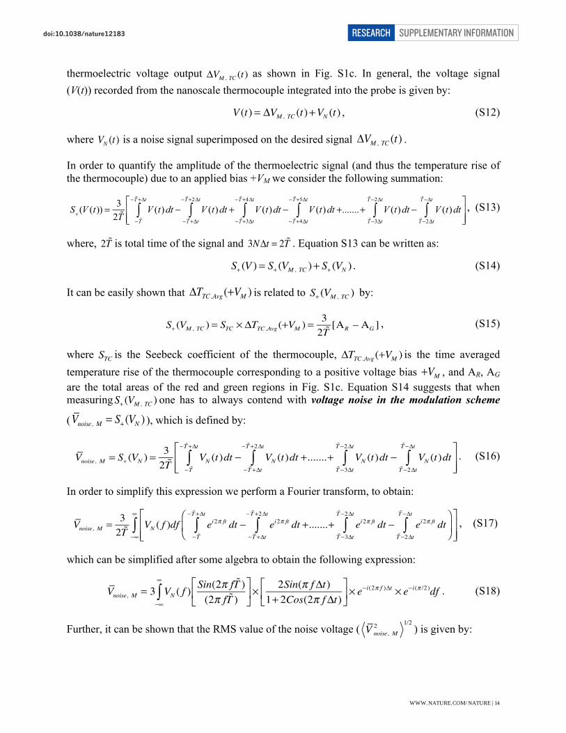
thermoelectric voltage output ΔVM , TC (t) as shown in Fig. S1c. In general, the voltage signal (V(t)) recorded from the nanoscale thermocouple integrated into the probe is given by:
V (t) = ΔVM , TC (t)+VN (t) , (S12)
where VN (t) is a noise signal superimposed on the desired signal ΔVM , TC (t) .
In order to quantify the amplitude of the thermoelectric signal (and thus the temperature rise of the thermocouple) due to an applied bias +VM we consider the following summation:
S+ (V (t)) = 3
2 TV (t)dt −
− T
− T+Δt
∫ V (t)dt +− T+Δt
− T+2Δt
∫ V (t)dt −− T+3Δt
− T+4Δt
∫ V (t)dt +− T+4Δt
− T+5Δt
∫ .......+ V (t)dtT−3Δt
T−2Δt
∫ − V (t)dtT−2Δt
T−Δt
∫⎡
⎣⎢⎢
⎤
⎦⎥⎥, (S13)
where, 2 T is total time of the signal and 3NΔt = 2 T . Equation S13 can be written as:
S+ (V ) = S+ (VM , TC )+ S+ (VN ) . (S14)
It can be easily shown that ΔTTC ,Avg (+VM ) is related to S+ (VM , TC ) by:
S+ (VM , TC ) = STC × ΔTTC ,Avg (+VM ) = 3
2 T[AR – AG ] , (S15)
where STC is the Seebeck coefficient of the thermocouple, ΔTTC ,Avg (+VM ) is the time averaged temperature rise of the thermocouple corresponding to a positive voltage bias +VM , and AR, AG are the total areas of the red and green regions in Fig. S1c. Equation S14 suggests that when measuringS+ (VM , TC ) one has to always contend with voltage noise in the modulation scheme
(Vnoise, M = S+ (VN ) ), which is defined by:
Vnoise, M = S+ (VN ) =
32 T
VN (t)dt −− T
− T +Δt
∫ VN (t)dt +− T +Δt
− T +2Δt
∫ .......+ VN (t)dtT −3Δt
T −2Δt
∫ − VN (t)dtT −2Δt
T −Δt
∫⎡
⎣⎢⎢
⎤
⎦⎥⎥
. (S16)
In order to simplify this expression we perform a Fourier transform, to obtain:
Vnoise, M = 3
2 TVN ( f )df ei2π ft dt −
− T
− T +Δt
∫ ei2π ft dt +− T +Δt
− T +2Δt
∫ .......+ ei2π ft dtT −3Δt
T −2Δt
∫ − ei2π ft dtT −2Δt
T −Δt
∫⎛
⎝⎜
⎞
⎠⎟
⎡
⎣⎢⎢
⎤
⎦⎥⎥−∞
∞
∫ , (S17)
which can be simplified after some algebra to obtain the following expression:
Vnoise, M = 3 VN ( f )
Sin(2π f T )(2π f T )
⎡
⎣⎢
⎤
⎦⎥
−∞
∞
∫ × 2Sin(π fΔt)1+ 2Cos(2π fΔt)⎡⎣⎢
⎤⎦⎥× e− i(2π f )Δt × e− i(π /2)df . (S18)
Further, it can be shown that the RMS value of the noise voltage ( V 2noise, M
1/2) is given by:
SUPPLEMENTARY INFORMATIONRESEARCHdoi:10.1038/nature12183
WWW.NATURE.COM/NATURE | 14
V 2
noise, M
1/2= STC × ΔTNoise, RMS (+VM ) ~ GN ( f )
Sin(2π f T )(2π f T )
⎡
⎣⎢
⎤
⎦⎥
−∞
∞
∫2
× 6Sin(π fΔt)1+ 2Cos(2π fΔt)⎡⎣⎢
⎤⎦⎥
2
df⎡
⎣⎢⎢
⎤
⎦⎥⎥
1/2
= GN ( f )
Sin(2π f T )(2π f T )
⎡
⎣⎢
⎤
⎦⎥
0
∞
∫2
× 6Sin(π fΔt)1+ 2Cos(2π fΔt)⎡⎣⎢
⎤⎦⎥
2
df⎡
⎣⎢⎢
⎤
⎦⎥⎥
1/2
, (S19)
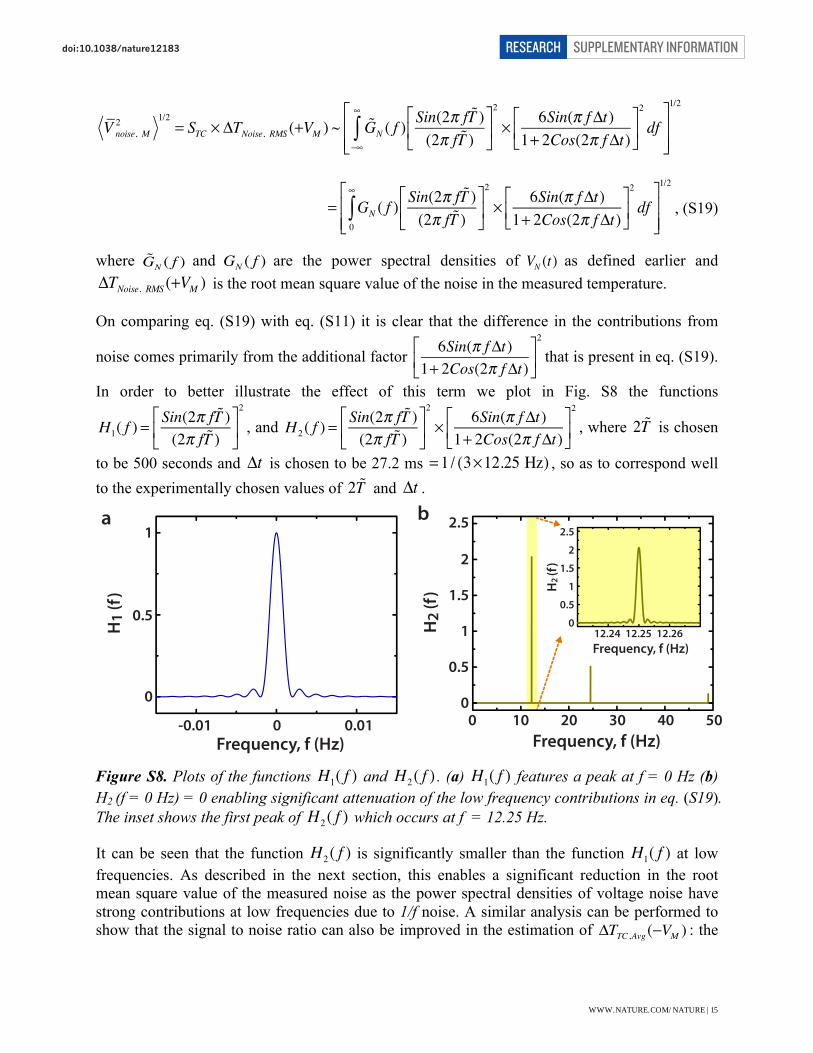
where GN ( f ) and GN ( f ) are the power spectral densities of VN (t) as defined earlier and ΔTNoise, RMS (+VM ) is the root mean square value of the noise in the measured temperature.
On comparing eq. (S19) with eq. (S11) it is clear that the difference in the contributions from
noise comes primarily from the additional factor 6Sin(π fΔt)1+ 2Cos(2π fΔt)⎡⎣⎢
⎤⎦⎥
2
that is present in eq. (S19).
In order to better illustrate the effect of this term we plot in Fig. S8 the functions
H1( f ) =
Sin(2π f T )(2π f T )
⎡
⎣⎢
⎤
⎦⎥
2
, and H2 ( f ) =
Sin(2π f T )(2π f T )
⎡
⎣⎢
⎤
⎦⎥
2
× 6Sin(π fΔt)1+ 2Cos(2π fΔt)⎡⎣⎢
⎤⎦⎥
2
, where 2 T is chosen
to be 500 seconds and Δt is chosen to be 27.2 ms = 1/ (3×12.25 Hz) , so as to correspond well to the experimentally chosen values of 2 T and Δt .
Figure S8. Plots of the functions H1( f ) and H2 ( f ) . (a) H1( f ) features a peak at f = 0 Hz (b) H2 (f = 0 Hz) = 0 enabling significant attenuation of the low frequency contributions in eq. (S19). The inset shows the first peak of H2 ( f ) which occurs at f = 12.25 Hz.
It can be seen that the function H2 ( f ) is significantly smaller than the function H1( f ) at low frequencies. As described in the next section, this enables a significant reduction in the root mean square value of the measured noise as the power spectral densities of voltage noise have strong contributions at low frequencies due to 1/f noise. A similar analysis can be performed to show that the signal to noise ratio can also be improved in the estimation of ΔTTC ,Avg (−VM ) : the
2.5
Frequency, f (Hz)0.01-0.01 0
0
0.5
1
Frequency, f (Hz)0 10 20 30 40 50
H2
(f)
0
0.5
1
1.5
2
Frequency, f (Hz)12.25 12.2612.24
H2
(f)
0
1
0.5
1.5
2
2.5a b
H1
(f)
SUPPLEMENTARY INFORMATIONRESEARCHdoi:10.1038/nature12183
WWW.NATURE.COM/NATURE | 15

time averaged temperature rise of the thermocouple corresponding to a negative voltage bias −VM . Finally, we note that ΔTTC ,Avg (−VM ) can be obtained from the following expression:
STC × ΔTTC ,Avg (−VM ) = 3
2 T[AB – AG ] , (S20)
where AB and AG are the total areas of the blue and green regions in Fig. S1c.
6.3 Unprocessed and Processed Data Obtained in the Experiments
The above discussion provides simple expressions (eq. S15 and eq. S20) for estimating the time averaged temperature rise of the thermocouple from the measured data. However, such an approach does not enable easy visualization of the temperature asymmetry. In this section we address the following question: can the asymmetric temperature response of the thermocouple be visually accessed from the raw data, at least for high power dissipations, where the temperature rises corresponding to positive and negative biases ΔTTC ,Avg (+VM ) and ΔTTC ,Avg (−VM ) respectively, as well as their differences are relatively large?
In order to answer this question, we begin by noting that the largest temperature rise (corresponding to molecular junctions) reported in the manuscript is ~15 mK. This implies that the corresponding modulated thermoelectric voltage output is STC × 15 mK = 245 nV, where STC = 16.3 ± 0.2 µV/K. Given the power spectral density of the electronic noise from the thermocouple (Fig. S12, see section 6.4 for details) the RMS value of noise in a 1 kHz bandwidth can be estimated to be a few microvolts (i.e. the RMS value of temperature noise is a few hundred millikelvin). We note that all the thermoelectric voltage measurements were performed at a sampling rate of 2 kHz after low pass filtering the signal at a cut-off frequency of 1 kHz to prevent aliasing of higher frequency noise into the signal (hence the choice of the 1 kHz bandwidth above). Given that the RMS value of temperature noise is an order of magnitude larger than the temperature signal it is to be expected that it would not be possible to visually see the modulated temperature signal from a time trace of the thermoelectric voltage obtained in one period of the measurement (1/12.25 s).
In order to demonstrate the assertions made above we show one-period of a three-level voltage signal corresponding to a modulation amplitude of 1.27 V in Fig. S9a. This represents the voltage bias applied across Au-BDNC-Au junctions in measurements with the highest power dissipation (QTotal, Avg = 0.35 µW). A representative electrical current measured in such an experiments is shown in Fig. S9b. In Fig. S9c, we show a measured thermoelectric voltage signal (converted to temperature from the known STC), which was offset to ensure that the mean value of the voltage corresponding to the region where no bias is applied (region shaded in green) is zero: this offset arises from the small temperature difference that exists between the NTISTP and the ambient. As expected, it is not possible to visually delineate the temperature signal corresponding to the applied biases from the data shown in Fig. S9c. However, it is clear that if the noise is random it would be possible to dramatically increase the signal to noise ratio by averaging all the temperature signals obtained in individual experiments such as those shown in Fig. S9c. In order to demonstrate this, we show in Fig. S9d an averaged temperature signal obtained from 122 individual experiments (~10 seconds of data). The averaging is performed by first superimposing the measured temperature signals from a series of experiments such that the
SUPPLEMENTARY INFORMATIONRESEARCHdoi:10.1038/nature12183
WWW.NATURE.COM/NATURE | 16

start and end points align. Subsequently, the voltages corresponding to each point on the x-axis are averaged to obtain the desired curve. It can be clearly seen that the noise on the temperature signal decreases upon averaging.
In Fig. S9e we present the averaged temperature data obtained from 100 seconds of data (1225 individual experiments). It can be clearly seen that the noise is significantly attenuated and the temperature signal corresponding to positive and negative biases is different. Finally, in Fig. S9f we present the temperature data obtained from 500 seconds of data (6125 individual experiments). From this data, it can be clearly seen that the temperature rise corresponding to positive and negative biases is different and is ~15 mK for a positive bias and ~10 mK corresponding to a negative bias. More accurate numbers can be obtained by averaging the temperature rise corresponding to positive and negative biases (see discussion in the last paragraph below). Such an analysis suggests that the average temperature rise corresponding to a positive bias is 10.3 mK (represented by a blue long-dashed line in Fig. S9f) and that corresponding to a negative bias is 15.2 mK (represented by a green short-dashed line in Fig. S9f). Further, the standard deviations corresponding to these averages are 0.6 mK for both positive and negative biases. These values are in excellent agreement with those reported in Fig. 2b of the manuscript.
In Fig. S10 and Fig. S11, we present otherwise identical data, corresponding to the highest average power dissipation (0.35 µW), obtained in the case of Au-BDA-Au and Au-Au junctions, respectively. In Fig. S10 it can be immediately seen that the temperature rise corresponding to a positive bias (+0.82 V) is larger than the temperature rise corresponding to a negative bias (-0.82 V). In contrast, for the Au-Au data shown in Fig. S11, the temperature rise corresponding to both positive (+0.067 V) and negative (-0.067 V) biases is identical within experimental uncertainty. Further, the temperature rise corresponding to positive and negative biases obtained by averaging the data shown in Figs. S10 & S11 as well as the standard deviations corresponding to the averages are in excellent agreement with those reported in Figs. 3b & 4a of the manuscript.
Before we conclude, we would like to emphasize an important point. It can be seen from the data shown in Figs. S9f, S10f, & S11f that the temperature change corresponding to the positive and the negative biases is relatively constant at all periods of time—this is a reflection of the extremely fast thermal time constant of the NTISTP (estimated to be ~10 µs in sec. 4.2). This suggests that further averaging can be performed on the data to accomplish greater noise reduction. For example, it is possible to average the 22 data points from the 2 ms – 24 ms (two data points at the beginning and at the end of the data can be excluded to roll-off effects from the low pass filter) to obtain a more accurate estimate of the temperature response corresponding to a positive bias. Similarly, it is possible to average 22 data points from 46 ms – 78 ms to get a more accurate estimate of the temperature response due to a negative bias. This is very similar to what is accomplished by eq. S15 and eq. S20, enabling us to determine the temperature changes in the thermocouple with excellent resolution (<0.3 mK)—this is key to extracting the temperature change of the thermocouple in measurements at the lowest power dissipation (0.07 µW). In the next sections, we describe a series of measurements that were performed to unambiguously determine the noise floor of our measurement scheme.
SUPPLEMENTARY INFORMATIONRESEARCHdoi:10.1038/nature12183
WWW.NATURE.COM/NATURE | 17

Figure S9. Raw and averaged data obtained in heat dissipation studies of Au-BDNC-Au junctions corresponding to a QTotal, Avg of 0.35 µW. (a) The three level voltage signal with an amplitude of 1.27 V. (b) The resultant current and (c) The temperature signal from the thermocouple (voltage output of the thermocouple divided by STC) in one period. The temperature signal obtained by averaging 10 s of data (~122 periods), 100 s of data (1225 periods), and 500 s of data (6125 periods) are shown in (d), (e), and (f), respectively. It can be seen that the average temperature rise is larger for a negative bias than a positive bias. From (f) the average temperature rise corresponding to a positive bias (blue long-dashed line) is estimated to be 10.3 mK and that corresponding to a negative bias (green short-dashed line) is estimated to be 15.2 mK. Further, the standard deviations corresponding to these averages are 0.6 mK for both positive and negative biases. These values are in excellent agreement with those reported in Fig. 2b of the manuscript.
0 20 40 60 80Time (milliseconds)
0
15
0
15
0
25
0300
-300
!TTC (mK)
!TTC (mK)
!TTC (mK)
!TTC (mK)
I (µA)
V (V)a
b
c
d
e
f
1.27
-1.270
0.30
-0.3
6125 periods
1225 periods
122 periods
1 period
SUPPLEMENTARY INFORMATIONRESEARCHdoi:10.1038/nature12183
WWW.NATURE.COM/NATURE | 18

Figure S10. Same as Fig. S9 but for Au-BDA-Au junctions. From (f) the average temperature rise corresponding to a positive bias is 13.9 mK (blue long-dashed line) and that corresponding to a negative bias is 11.6 mK (green short-dashed line). Further, the standard deviations corresponding to these averages are 0.6 mK for both positive and negative biases. These values are in excellent agreement with those reported in Fig. 3b of the manuscript.
6125 periods
0 20 40 60 80Time (milliseconds)
1225 periods
122 periods
0
15
0
15
0
25
1 period
0300
-300
!TTC (mK)
!TTC (mK)
!TTC (mK)
!TTC (mK)
I (µA)
V (V)a
b
c
d
e
f
0.82
-0.82
0
0.40
-0.4
SUPPLEMENTARY INFORMATIONRESEARCHdoi:10.1038/nature12183
WWW.NATURE.COM/NATURE | 19

Figure S11. Same as Fig. S9 but for Au-Au atomic junctions. From (f) the average temperature rise corresponding to both positive and negative biases is 12.7 mK (the blue and green dashed lines representing the means overlap). Further, the standard deviations corresponding to these averages are 0.4 mK for both positive and negative biases. These values are identical to that reported in Fig. 4a of the manuscript.
0 20 40 60 80Time (milliseconds)
0
15
0
15
0
25
0300
-300
!TTC (mK)
!TTC (mK)
!TTC (mK)
!TTC (mK)
I (µA)
V (V)a
b
c
d
e
f
0.067
-0.0670
50
-5
6125 periods
1225 periods
122 periods
1 period
SUPPLEMENTARY INFORMATIONRESEARCHdoi:10.1038/nature12183
WWW.NATURE.COM/NATURE | 20

6.4 Experimentally Measured Power Spectral Density of Voltage Noise of the Thermocouple and Estimate of ΔTNoise, RMS
In order to estimate the temperature noise using eq. (S19) it is necessary to measure the power spectral density (PSD) of the thermoelectric voltage noise of the integrated thermocouple. Figure S12 shows the measured PSD of the thermocouple, obtained using a commercially available spectrum analyzer (SR760, Stanford Research System). The measured PSD is found to be large at low frequencies, showing a 1/f behavior. Using eq. (S19) in conjunction with the measured PSD we estimate that ΔTNoise, RMS associated with the nanoscale thermocouple is ~50 µK. In performing these estimates, the values of 2 T and Δt were chosen to be 500 seconds and 27.2 ms = 1/(3×12.25 Hz), respectively, so as to correspond well to the values of 2 T and Δt used in the experiments.
Figure S12. The measured one-sided power spectral density (PSD) of the thermocouple voltage noise (0 – 50 Hz). The inset shows the measured PSD in a larger range frequencies (0 – 1 kHz).
In order to check the accuracy of the estimate we analyzed the RMS value of the measured noise using a second approach. Specifically, we recorded the noise voltage from the thermocouple for a period of 500 seconds, in a bandwidth of 1 kHz, and computed Vnoise, M (the voltage noise in the
modulation scheme) using eq. (S16). This was repeated ten times to obtain Vnoise, M (i), i = 1:10
to compute the RMS values of the voltage noise V 2noise, M
1/2= V noise, M (i)( )
i=1
10
∑2
10⎡
⎣⎢⎢
⎤
⎦⎥⎥
12
and the
corresponding temperature noise which were found to be 0.5 nV and ~30 µK respectively. This value is in reasonable agreement with the estimated RMS temperature resolution from the
Frequency, f (Hz)0 10 20 30 40 50Po
wer
spec
tral
den
sity
, GN
(f)
(n
V2 /Hz)
100
1000
Frequency, f (kHz)Pow
er sp
ectr
al d
ensi
ty
GN
(f) (
nV2 /H
z)
0 0.2 0.4 0.6 0.8 110
100
1000
SUPPLEMENTARY INFORMATIONRESEARCHdoi:10.1038/nature12183
WWW.NATURE.COM/NATURE | 21

frequency domain analysis and confirms the validity of eq. (S19). Taken together, these estimates suggest that the uncertainty in the measured temperature due to electronic noise is ~50 µK. 6.5 Quantification of the Effect of Capacitive Coupling
In addition to the electronic noise described above the capacitive coupling between the thermocouple leads and the substrate also results in a spurious signal. The effect of capacitive coupling is to generate a noise signal that is indistinguishable from the thermoelectric voltage signal of the thermocouple. Fig. S13a schematically shows a circuit diagram that represents the capacitive coupling between the substrate and the NTISTP by three capacitors: the capacitor C1 represents the capacitive coupling between the substrate and the outer Au electrode, C2 represents the capacitive coupling between the outer Au electrode and the Cr electrode of the thermocouple, and C3 represents the capacitive coupling between the Cr and inner Au electrode. The resistors R1, R2, R3 shown in Fig. S13a represent the electrical resistances in the leads of the NTISTP. The data provided below are well accounted for by this simple model.
In order to quantify the effect of capacitive coupling, we performed a series of experiments in which the tip of the NTISTP was placed in close proximity of the substrate (~5 nm), while a modulated sinusoidal signal was supplied to the substrate as shown in Fig. S13b. Here, a sinusoidal signal is chosen instead of the three level modulation scheme due to the simplicity of analyzing sinusoidal signals. In the first set of experiments the frequency of modulation was chosen to be 12.25 Hz and the sinusoidal voltage output from the thermocouple was monitored using a lock-in amplifier (SR 830) as the amplitude of the input sinusoidal signal was systematically varied (0 V – 7.5 V). Figure S13c shows the results obtained in these experiments where the voltage output is seen to increase proportionally with the voltage input. We note that in these experiments the resistance between the tip and the substrate is very large (>1 GΩ), therefore, the electrical current through the tip-substrate junction is negligible resulting in insignificant amount of Joule heating. Hence, the measured voltage output is primarily due to capacitive coupling and electronic noise.
In addition to these experiments, we studied the frequency dependence of capacitive coupling. Specifically, we performed an experiment where the amplitude of the sinusoidal signal supplied to the substrate was held constant at 1.5 V while the frequency of the sinusoidal signal was systematically varied. The voltage output measured across the thermocouple junction in these experiments is shown in Fig. S13d. It can be seen that the voltage output increases quadratically with frequency. This result may seem surprising at first sight as one would naively expect a linear dependence on frequency when the coupling is capacitive50. The quadratic dependence can be understood by noting that in our set up there are multiple levels of capacitive coupling: first the substrate is coupled to the outer electrode of the NTISTP (via C1, see Fig. S13a) and the outer electrode is subsequently capacitively coupled to the inner Cr electrode via capacitor C2 and finally there is resistive (through the contact at the apex) and capacitive coupling between the Cr and inner Au electrode. A detailed analysis of this circuit configuration shows that the voltage output across the thermocouple should indeed be quadratically dependent on the frequency.
Finally, we performed experiments on ~5 nm NTISTP-substrate gaps using a three level modulation scheme (Fig. S13e). These experiments aim to quantify the dependence of measured (capacitively coupled) voltage noise on both the voltage bias and the time period of
SUPPLEMENTARY INFORMATIONRESEARCHdoi:10.1038/nature12183
WWW.NATURE.COM/NATURE | 22

measurements. First, to understand the effect of the total time of measurement 2 T (see Fig. S1a) on the voltage noise due to capacitive coupling we applied a three-level modulation signal with VM = 1.5 V for 500 seconds. This was repeated 10 times while recording the voltage output from the thermocouple. The data obtained in each of these experiments was analyzed to compute Vnoise, M (+VM / −VM ) and V 2
noise, M (+VM / −VM )1/2
from which the apparent RMS temperature due to capacitive coupling (ΔTApp, Capacitive, RMS (+VM / −VM )) was obtained using
V 2
noise, M (+VM / −VM )1/2
= STC × ΔTApp, Capacitive, RMS (+VM / −VM ) . This was repeated for a range of
modulation voltages and time periods to obtain the data shown in Fig. S13f where ΔTApp, Capacitive, RMS (+VM ) is shown for various time periods of measurements and bias voltages. We note that the RMS values for negative biases are identical and not shown. It can be seen that the RMS values decrease as the total time of the measurement increases but eventually becomes constant for measurements longer than ~200 seconds (as expected from eq. (S19)). It can be seen that the largest RMS value occurs for an amplitude of 1.5 V and is ~0.3 mK.
In the inset of Fig. S13f we plot ΔTApp, Capacitive, RMS obtained from experiments where the modulation voltages were systematically varied while keeping the frequency of modulation and the total time of measurement fixed at 12.25 Hz and 500 seconds respectively. It can be seen from the figure that the RMS noise voltages increase linearly as the applied bias voltage is increased. Further, it can be seen that for a modulation voltage of ~1.5 V (the largest bias applied in the experiments) the RMS temperature noise is ~0.3 mK. Therefore, it is clear that the largest uncertainty introduced by capacitive coupling is ~0.3 mK and occurs at the largest applied bias. We also note that when VM = 0 V the measured RMS noise in the temperature is ~30 µK and is consistent with the analysis provided in the earlier section. Taken together these experiments suggest that capacitive coupling does not contribute significantly if a sufficiently low modulation frequency is employed. However, if a higher modulation frequency is selected the effect of capacitive coupling can become substantial.
The data shown in the inset of Fig. S13f along with the discussion provided in section 6.4 unambiguously proves that the noise equivalent temperature for the chosen modulation scheme is ~0.3 mK at the highest voltage bias (1.5 V), ~0.1 mK at the lowest bias (0.45 V) employed in studying heat dissipation in molecular junctions, and ~50 - 100 µK at the lowest biases (30 mV) employed for probing heat dissipation in Au-Au junctions.
SUPPLEMENTARY INFORMATIONRESEARCHdoi:10.1038/nature12183
WWW.NATURE.COM/NATURE | 23

Figure S13. Quantification of the effect of capacitive coupling. (a) Schematic of a simplified circuit diagram describing the origin of capacitive coupling. (b) Experimental setup to quantify the capacitive coupling: A sinusoidal voltage is applied across the junction. (c) Measured amplitude of the voltage output across the thermocouple as the amplitude of the sinusoidal signal (12.25 Hz) is increased. (d) Measured amplitude of the voltage output across the thermocouple as the frequency of the sinusoidal signal is increased while keeping the amplitude fixed at 1.5 V. (e) Experimental setup to quantify the capacitive coupling when a three level modulation scheme is used. (f) Measured RMS temperature noise as a function of the total time of the measurement for various voltage biases (0 V – 1.5 V). The inset shows the measured RMS temperature noise as a function of the amplitude of modulation voltages for 500 seconds long measurements.
a b
c d
SiO 2
tip
Au substrate
~5 nm
Au SiN x
AuSiN x
Cr
Bias
!VNoise
e f
!VNoise
Au substrate
Bias
Cr
Au
Au
C2
C1
C3
R1
R2
R3
SiO 2
tip
Au substrate
~5 nm
Au SiN x
AuSiN x
Cr
Bias
!VNoise
Amplitude (V)
!Tno
ise (
mK)
0 1.5 3 4.5 6 7.5
0.8
0.6
0.4
0.2
0
Frequency = 12.25 Hz
Frequency (Hz)
!Tno
ise (
mK)
0 49 98 147
2
1
0
Time (sec)0 100 200 300 400 500
0 V0.3 V0.6 V0.9 V1.2 V1.5 V
!TAp
p, C
apac
itive
, RM
S (m
K)
0
0.5
1
1.5
2
Bias (V)0 0.3 0.6 0.9 1.51.2
00.05
0.3
0.15
0.250.2
0.1
!TAp
p, C
apac
itive
, RM
S (m
K)
Amplitude = 1.5 V
SUPPLEMENTARY INFORMATIONRESEARCHdoi:10.1038/nature12183
WWW.NATURE.COM/NATURE | 24

6.6 Quantification of the Statistical Variations in ΔTTC ,Avg (+VM ) and ΔTTC ,Avg (−VM ) due to Fluctuations in the Microscopic Characteristics of Atomic-scale Junctions
The overall uncertainty in the reported temperature rise shown in Figures 2, 3, 4 of the main manuscript arises from electronic noise, capacitive coupling and stochastic fluctuations in the transmission characteristics of atomic and molecular junctions. The contributions of the electronic noise and capacitive coupling have been quantified above. Here, we discuss the variations introduced by stochastic fluctuations on the measured ΔTTC ,Avg (+VM ) and ΔTTC ,Avg (−VM ) . As described in the manuscript the heat dissipation per unit time in the left electrode of the junction (QL (V ) ) is given by:
QL (V ) =2h
(µL − E)τ (E,V )[ f (E,µL )− f (E,µR )]−∞
∞
∫ dE . (S21)
Further, a similar expression can be obtained for the power dissipation in the right electrode (QR(V )) . However, in the experiments the power dissipated in each of the electrodes fluctuates due to the microscopic variations in the junctions. Specifically, since the transmission function τ (E,V ,t) is time dependent (due to variations in junction geometry) the instantaneous power dissipation given by:
QL (V ,t) =2h
(µL − E)τ (E,V ,t)[ f (E,µL )− f (E,µR )]−∞
∞
∫ dE . (S22)
The effect of stochastic fluctuations can be quantified by considering a series of experiments where the heat dissipation in molecular junctions is studied using a modulation scheme for a time period of 2 T seconds in each of the experiments. Even if the amplitude of the modulation scheme (VM ) is kept constant to ensure that the averaged total power dissipation is the same in each experiment the averaged power dissipation in any given electrode can vary from one experiment to another due to fluctuations in the transmission characteristics. This, in turn, results in fluctuations in the measured ΔTTC ,Avg (+VM ) and ΔTTC ,Avg (−VM ) from one experiment to another. In order to quantify these fluctuations, we reanalyzed the data obtained in the measurements of heat dissipation in AMJs. The 500 s long data corresponding to each of the data points in Figs. 2b, 3b, and 4a of the main manuscript was split into five equal parts (each 100 s long). Subsequently, we analyzed each of the five sets of data using Eqs. (S15) & (S20) to obtain five different values of ΔTTC, Avg. From these data, we computed the mean and standard deviation of ΔTTC, Avg for positive and negative biases. We note that the mean values obtained in this analysis are identical to the values obtained by analyzing the ~500 s long data as reported in Figs. 2b, 3b, and 4a. The results of this analysis for Au atomic junctions are shown in Fig. S14a. As can be seen from the data, the standard deviations are imperceptible and are <0.1 mK for Au atomic junctions. The
SUPPLEMENTARY INFORMATIONRESEARCHdoi:10.1038/nature12183
WWW.NATURE.COM/NATURE | 25
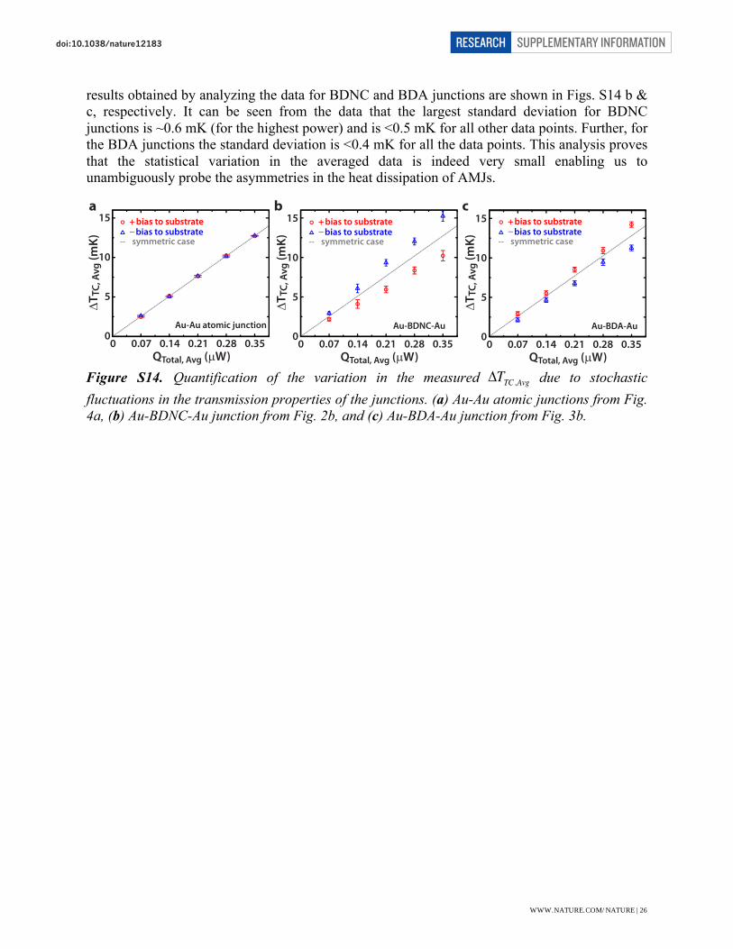
results obtained by analyzing the data for BDNC and BDA junctions are shown in Figs. S14 b & c, respectively. It can be seen from the data that the largest standard deviation for BDNC junctions is ~0.6 mK (for the highest power) and is <0.5 mK for all other data points. Further, for the BDA junctions the standard deviation is <0.4 mK for all the data points. This analysis proves that the statistical variation in the averaged data is indeed very small enabling us to unambiguously probe the asymmetries in the heat dissipation of AMJs.
Figure S14. Quantification of the variation in the measured ΔTTC ,Avg due to stochastic fluctuations in the transmission properties of the junctions. (a) Au-Au atomic junctions from Fig. 4a, (b) Au-BDNC-Au junction from Fig. 2b, and (c) Au-BDA-Au junction from Fig. 3b.
a b c
QTotal, Avg (µW)0 0.07 0.14 0.28 0.35
5
15
0
10
0.21
!TTC
, Avg
(mK)
bias to substratebias to substrate
symmetric case_+
Au-BDNC-Au
bias to substratebias to substrate
symmetric case_+
QTotal, Avg (µW)0 0.07 0.14 0.28 0.35
5
15
0
10
0.21
!TTC
, Avg
(mK)
Au-BDA-Au
15
QTotal, Avg (µW)0 0.07 0.14 0.28 0.35
5
0
10
0.21
!TTC
, Avg
(mK)
Au-Au atomic junction
bias to substratebias to substrate
symmetric case_+
SUPPLEMENTARY INFORMATIONRESEARCHdoi:10.1038/nature12183
WWW.NATURE.COM/NATURE | 26

Reference and Notes: 31 Kim, K., Jeong, W. H., Lee, W. C. & Reddy, P. Ultra-high vacuum scanning thermal
microscopy for nanometer resolution quantitative thermometry. ACS Nano 6, 4248-4257 (2012).
32 Taylor, J., Brandbyge, M. & Stokbro, K. Theory of rectification in tour wires: The role of electrode coupling. Phys. Rev. Lett. 89, 138301 (2002).
33 Ahlrichs, R., Bär, M., Häser, M., Horn, H. & Kölmel, C. Electronic-structure calculations on workstation computers - the program system turbomole. Chem. Phys. Lett. 162, 165-169 (1989).
34 Perdew, J. P. Density-functional approximation for the correlation-energy of the inhomogeneous electron-gas. Phys. Rev. B 33, 8822-8824 (1986).
35 Schäfer, A., Horn, H. & Ahlrichs, R. Fully optimized contracted Gaussian basis sets for atoms Li to Kr. J. Chem. Phys. 97, 2571-2577 (1992).
36 Ward, D. R., Hüser, F., Pauly, F., Cuevas, J. C. & Natelson, D. Optical rectification and field enhancement in a plasmonic nanogap. Nature Nanotech. 5, 732-736 (2010).
37 Gilman, Y., Allen, P. B. & Hybertsen, M. S. Density-functional study of adsorption of isocyanides on a gold(111) surface. J. Phys. Chem. C 112, 3314-3320 (2008).
38 Dahlke, R. & Schollwöck, U. Electronic transport calculations for self-assembled monolayers of 1,4-phenylene diisocyanide on Au(111) contacts. Phys. Rev. B 69, 085324 (2004).
39 Quek, S. Y. et al. Amine-gold linked single-molecule circuits: Experiment and theory. Nano Lett. 7, 3477-3482 (2007).
40 Li, Z. & Kosov, D. S. Nature of well-defined conductance of amine-anchored molecular junctions: Density functional calculations. Phys. Rev. B 76, 035415 (2007).
41 Strange, M., Rostgaard, C., Häkkinen, H. & Thygesen, K. S. Self-consistent GW calculations of electronic transport in thiol- and amine-linked molecular junctions. Phys. Rev. B 83, 115108 (2011).
42 Roh, H. H. et al. Novel nanoscale thermal property imaging technique: The 2 omega method. I. Principle and the 2 omega signal measurement. J. Vac. Sci. Tech. B 24, 2398-2404 (2006).
43 Segal, D., Nitzan, A. & Hänggi, P. Thermal conductance through molecular wires. J. Chem. Phys. 119, 6840-6855 (2003).
44 Losego, M. D., Grady, M. E., Sottos, N. R., Cahill, D. G. & Braun, P. V. Effects of chemical bonding on heat transport across interfaces. Nature Mater. 11, 502-506 (2012).
45 Wang, R. Y., Segalman, R. A. & Majumdar, A. Room temperature thermal conductance of alkanedithiol self-assembled monolayers. Appl. Phys. Lett. 89, 173113 (2006).
46 Sergueev, N., Shin, S., Kaviany, M. & Dunietz, B. Efficiency of thermoelectric energy conversion in biphenyl-dithiol junctions: Effect of electron-phonon interactions. Phys. Rev. B 83, 195415 (2011).
47 Ziman, J. M. Principles of the theory of solids. 2d edn, (University Press, 1972). 48 Zhou, F., Persson, A., Samuelson, L., Linke, H. & Shi, L. Thermal resistance of a
nanoscale point contact to an indium arsenide nanowire. Appl. Phys. Lett. 99, 063110 (2011).
49 Shen, S., Mavrokefalos, A., Sambegoro, P. & Chen, G. Nanoscale thermal radiation between two gold surfaces. Appl. Phys. Lett. 100, 233114 (2012).
50 Ott, H. W. Noise reduction techniques in electronic systems. (Wiley, 1988).
SUPPLEMENTARY INFORMATIONRESEARCHdoi:10.1038/nature12183
WWW.NATURE.COM/NATURE | 27