
STUDY,FABRICATIONANDCHARACTERIZATION ... · general features of these structures will be introduced...
148
Transcript of STUDY,FABRICATIONANDCHARACTERIZATION ... · general features of these structures will be introduced...

Dipartimento di Elettronica, Laboratoire de Physique de laInformatica e Sistemistica Matière CondenséeUniversità di Bologna Université de Nice-Sophia Antipolis
Dottorato di Ricerca in Ingegneria Pour obtenir le grade deElettronica, Informatica Docteur dans lae delle Telecomunicazioni Spécialité PhysiqueING-INF/02 - XIX Ciclo
STUDY, FABRICATION AND CHARACTERIZATIONOF SEGMENTED WAVEGUIDES FOR ADVANCEDPHOTONIC COMPONENTS ON LITHIUM NIOBATE
Davide Castaldini
Relatore: Directeur de thèse:Prof. Paolo Bassi Prof. Pascal Baldi
Co-relatore: Co-directeur de thèse:Prof. Pascal Baldi Prof. Paolo Bassi
Rapporteurs:Dr Serge Valette
Dr Alain Barthelemy
Coordinatore Examinateurs:Prof. Paolo Bassi Prof. Fabrizio Frezza
Dott. Gian Giuseppe Bentini
Membrès invitésDr Marc de MicheliDr Pierre Aschieri
A.A. 2005/2006


Alla mia famiglia


Contents
Introduction 1
1 Segmented structures 51.1 Introduction . . . . . . . . . . . . . . . . . . . . . . . . . . . . . . . . 51.2 Propagation in periodic media . . . . . . . . . . . . . . . . . . . . . . 51.3 Equivalence theorem for periodic media . . . . . . . . . . . . . . . . . 71.4 Periodically segmented waveguides . . . . . . . . . . . . . . . . . . . 101.5 Propagation losses in periodically segmented waveguides . . . . . . . 111.6 Cutoff properties of periodically segmented waveguides . . . . . . . . 121.7 Segmented waveguides . . . . . . . . . . . . . . . . . . . . . . . . . . 15
1.7.1 Mode transformers: Taper . . . . . . . . . . . . . . . . . . . . 161.7.2 Mode filters . . . . . . . . . . . . . . . . . . . . . . . . . . . . 19
2 Numerical methods 232.1 Introduction . . . . . . . . . . . . . . . . . . . . . . . . . . . . . . . . 232.2 3D fully vectorial Beam Propagation Method . . . . . . . . . . . . . . 24
2.2.1 Finite difference schematization . . . . . . . . . . . . . . . . . 292.2.2 Crank-Nicholson method . . . . . . . . . . . . . . . . . . . . . 302.2.3 Perfect Matched Layer . . . . . . . . . . . . . . . . . . . . . . 312.2.4 BPM validation . . . . . . . . . . . . . . . . . . . . . . . . . . 342.2.5 Consideration on the non-unitarity of BPM operators . . . . . 38
2.3 Finite difference mode solver . . . . . . . . . . . . . . . . . . . . . . . 382.3.1 Mode solver validation . . . . . . . . . . . . . . . . . . . . . . 42
3 Device fabrication techniques 453.1 Introduction . . . . . . . . . . . . . . . . . . . . . . . . . . . . . . . . 453.2 Properties of Lithium Niobate . . . . . . . . . . . . . . . . . . . . . . 453.3 Waveguide fabrication . . . . . . . . . . . . . . . . . . . . . . . . . . 47
3.3.1 Soft Proton Exchange . . . . . . . . . . . . . . . . . . . . . . 483.4 Photolithography . . . . . . . . . . . . . . . . . . . . . . . . . . . . . 50
3.4.1 Photomask design . . . . . . . . . . . . . . . . . . . . . . . . . 533.5 Fabrication results . . . . . . . . . . . . . . . . . . . . . . . . . . . . 56

ii Contents
3.5.1 M-lines characterization . . . . . . . . . . . . . . . . . . . . . 583.6 Polishing . . . . . . . . . . . . . . . . . . . . . . . . . . . . . . . . . . 61
4 Characterization techniques 654.1 Introduction . . . . . . . . . . . . . . . . . . . . . . . . . . . . . . . . 654.2 Measuring attenuation, effective group index and mode size . . . . . . 654.3 Experimental setup . . . . . . . . . . . . . . . . . . . . . . . . . . . . 67
4.3.1 Loss measurements . . . . . . . . . . . . . . . . . . . . . . . . 684.3.2 Group index and dispersion measurements . . . . . . . . . . . 714.3.3 Mode size measurements . . . . . . . . . . . . . . . . . . . . . 75
4.4 Results . . . . . . . . . . . . . . . . . . . . . . . . . . . . . . . . . . . 77
5 Segmented Waveguide Taper 835.1 Introduction . . . . . . . . . . . . . . . . . . . . . . . . . . . . . . . . 835.2 Numerical design of the taper . . . . . . . . . . . . . . . . . . . . . . 84
5.2.1 Numerical modelling of Lithium Niobate waveguides . . . . . 855.2.2 Segmented waveguide design . . . . . . . . . . . . . . . . . . . 895.2.3 Taper design . . . . . . . . . . . . . . . . . . . . . . . . . . . 93
5.3 Device Fabrication . . . . . . . . . . . . . . . . . . . . . . . . . . . . 975.4 Experimental setup . . . . . . . . . . . . . . . . . . . . . . . . . . . . 975.5 Results . . . . . . . . . . . . . . . . . . . . . . . . . . . . . . . . . . . 985.6 Tapers in quantum relay . . . . . . . . . . . . . . . . . . . . . . . . . 101
6 Segmented waveguide mode filter 1056.1 Introduction . . . . . . . . . . . . . . . . . . . . . . . . . . . . . . . . 1056.2 Mode filter operation . . . . . . . . . . . . . . . . . . . . . . . . . . . 1056.3 Coupled Mode Theory for segmented waveguide mode filters . . . . . 1076.4 Experimental results . . . . . . . . . . . . . . . . . . . . . . . . . . . 112
Conclusions 120
Author’s references 124
Bibliography 126

Foreword
Before starting my thesis report, I would like to gratefully acknowledge theFrench-Italian University (http://www.universita-italo-francese.org/) for pro-viding a Vinci Program fellowship which allowed this work in the framework of aco-tutored PhD activity developed at DEIS (Dipartimento di Elettronica Informat-ica e Sistemistica) of the University of Bologna, Italy, and at LPMC (Laboratoirede Physique de la Matiere Condensee) of the University of Nice-Sophia Antipolis,France.
Davide Castaldini

Introduction
After their first demonstration, occurred in the first seventies, optical telecom-munications experienced a very rapid evolution, which has allowed dramatic changesnot only in the telecommunication networks [1], but also in the services which theyallow to provide to the final users.
The effort which has generated so rapid improvements has been twofold and doesnot seem concluded yet. From one side, new and then expensive technologies havebeen developed. Such technologies made available, for example, sources and detec-tors operating at always longer wavelengths, to take advantage of lower absorptionlosses of silica fibers, optical amplifiers, to allow transoceanic links with less re-peaters, high speed modulators, to modulate directly the optical signal, WavelengthDivision Multiplexing (WDM) systems [2], to transmit many independent channelson the same fiber and then increase the overall bandwidth. Research is not con-cluded, anyway, as there are still some bottlenecks which should be eliminated. Forexample, a cost effective way to perform all optical wavelength conversion or switch-ing and routing operations without high-speed electronic data processing which re-quires opto-electrical and electro-optical conversions has not yet been found. Tothis purpose new components, for example based on non linear effects [3], are underinvestigation.
But it must also be acknowledged that the attempts to advance technology be-yond its present limits are not the only challenge researchers have to face. Thewidespread application of optical technologies, in fact, has made cost reduction andease of operation an equally important issue. In view of a general system opti-mization, also the design of basic elements should then be reconsidered. A typicalexample is device pigtailing. Low loss connection of an optical fiber to an integratedoptical waveguide is a critical operation which requires time consuming alignmentprocedures and expensive micropositioning systems. However, for mass production,an easy operation with low positioning tolerances should be done to reduce cost andtime.
Coupling does not only introduce loss problems. In non linear optics and namelyin frequency conversion experiments, for example, waveguides which are monomodeat longer wavelengths are generally multimode at shorter ones [4]. The presence ofhigher order modes reduces the process efficiency. In these cases, it would then beimportant that the field coming from a shorter wavelength device could be trans-
2 Introduction
formed into the field of the long wavelength waveguide filtering higher order modesto avoid the drawbacks caused by their presence.
It is also worth to be noticed that the set up of new kind of transmission systemsand the efficient solution of basic problems may not be independent. For example,in transmission systems exploiting quantum properties of photons [5], allowing anew kind of information cryptography [6] and then attracting as they seem a goodsolution to the privacy problems, loss reductions can be obtained only by optimizingall the component as bits are associated to single photons (Qbit), which then cannotbe amplified with classical amplifiers as, in this case, all the information would belost.
The simple examples mentioned before show how the quest for new and simpleoptical devices has not yet reached its end. Instead of using time consuming oper-ations or huge technological efforts, a careful rethinking of the devices, exploitingnew structures or physical principles seems then the way to follow.
This thesis tackles the problem of conceiving, designing and realizing new devicesto solve the basic problem of obtaining low loss and efficient device coupling. Tothis purpose we considered the so called segmented waveguides . They are waveguideswith longitudinal variations of their refractive index. These variations can be notonly periodic, as it happens in gratings, or, more generally, in the so called PhotonicCrystals [7], but can also be suitably tailored. The versatility provided by theirmany degrees of freedom has suggested us to investigate if they could be a way tofabricate low loss couplers and mode filters.
This study has been carried out in all the steps necessary to demonstrate de-vices operation, starting from their design, exploiting theoretical features of thesecomponents also using suitable numerical techniques, through their fabrication andperforming also their characterization. The material chosen for the realization isLithium Niobate (LiNbO3), which is interesting for its low losses at the standardtelecommunications wavelengths and its good non linear as well as good electro-optics properties. We have then realized a setup suitable to evaluate the perfor-mances of the realized devices and compare them with the numerical predictions.Coupling losses reduction and mode filtering will be the particular examples in whichthe use of segmented waveguides will be proposed as a technologically simple andefficient solution to obtain the desired result to improve performances.
In chapter 1, the properties of the segmented waveguides will be studied first,introducing general principles with simple 1D models, and extending them to themore interesting cases of slab and channel waveguides. In chapter 2, numerical toolsdeveloped to model segmented waveguides in their 3D general structure will be in-troduced. After their design, segmented waveguide based devices have been realizedstarting from mask preparation up to device fabrication and characterization. Fabri-cation techniques will be described in chapter 3, while in chapter 4 the experimentalset up used for device characterization will be described. The measurement appa-ratus is an all-in-one set up conceived to evaluate not only propagation losses or

3
guided mode size but also effective group index and dispersion for both integratedoptical waveguides and optical fibers. In chapter 5 the results obtained for taperscharacterization will be described showing that segmented waveguides allow realiza-tion of couplers with coupling losses reduced by up to 0.78 dB. These devices havealso been successfully introduced, with similar performances, in a complex device forquantum communication like a quantum relay. In chapter 6 we will report resultsconcerning a modal filter designed to operate at the wavelength λ = 840 nm. Inparticular it will be described the design of the two tapers present in this componentin order to provide a fundamental mode transformation without the introduction ofhigher order modes. Finally conclusions will be drawn.

4 Introduction

1
Segmented structures
1.1 Introduction
In this chapter, the characteristics of electromagnetic field propagation in wave-guides with longitudinal changes of the refractive index will be described. Thegeneral features of these structures will be introduced starting from the case of peri-odically segmented waveguides , i.e. structures in which such changes are longitudi-nally periodic. The very simple case of 1D periodic structures will be preliminarilyused to determine analytically their dispersion curves and different possible opera-tion regimes. It will also be shown that many properties of these structures can bedetermined also studying an equivalent continuous structure. The obtained resultswill then be extended to 2D and 3D structures such as integrated optical slab orchannel waveguides. In the last part of the chapter we will relax the constraint ofregular periodicity and introduce the more general concept of segmented waveguidewhere period and other device parameters can be varied longitudinally. In thiscase the properties of periodic waveguides will be considered valid locally with thesame idea leading to define local normal modes in longitudinally varying continuousstructures. After reminding some well known applications of these structures, thepossible uses of segmented waveguides studied in this thesis will be introduced.
1.2 Propagation in periodic media
In order to show the properties of an electromagnetic field propagating througha periodic medium, a simple 1D model can be used [8, 9, 10, 11]. The structureis constituted by the regular repetition, with period P of layers alternatively withhigh (width equal to a) and low (width equal to b) refractive indices, with infinitedimensions in the two x and y directions orthogonal to z, as schematically illustratedin 1.1.
One of the most important parameters for the characterization of any optical
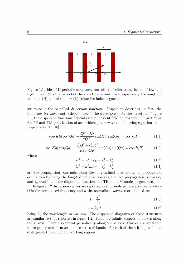
6 1. Segmented structures
P
H H HH L L L
Kz
Kx
x
z−a b
Figure 1.1: Ideal 1D periodic structure, consisting of alternating layers of low andhigh index. P is the period of the structure, a and b are respectively the length ofthe high (H) and of the low (L) refractive index segments.
structure is the so called dispersion function. Dispersion describes, in fact, thefrequency (or wavelength) dependence of the wave speed. For the structure of figure1.1, the dispersion functions depend on the incident field polarization. In particularfor TE and TM polarization of an incident plane wave the following equations holdrespectively [11, 10]:
cos(Kb) cos(Qa)− Q2 + K2
2QKsin(Kb) sin(Qa) = cos(kzP ) (1.1)
cos(Kb) cos(Qa)− ε2LQ2 + ε2
HK2
2εLεHQKsin(Kb) sin(Qa) = cos(kzP ) (1.2)
whereK2 = ω2µ0εL − k2
x − k2y (1.3)
Q2 = ω2µ0εH − k2x − k2
y (1.4)
are the propagation constants along the longitudinal direction z. If propagationoccurs exactly along the longitudinal direction (z), the two propagation vectors kx
and ky vanish and the dispersion functions for TE and TM modes degenerate.In figure 1.2 dispersion curves are reported in a normalized reference plane where
Ω is the normalized frequency and κ the normalized wavevector, defined as:
Ω =P
λ0
(1.5)
κ = kzP. (1.6)
being λ0 the wavelength in vacuum. The dispersion diagrams of these structuresare similar to that reported in figure 1.2. There are infinite dispersion curves alongthe Ω axis. They also repeat periodically along the κ axis. Curves are separatedin frequency and form an infinite series of bands. For each of them it is possible todistinguish three different working regions:

1.3 Equivalence theorem for periodic media 7
0 2 4 6 8 100
0.1
0.2
0.3
0.4
0.5
0.6
0.7
0.8
0.9
1
Normalized wave number k
Norm
aliz
ed fre
quency
W
Figure 1.2: Disperson curves for εL = 5ε0, εH = 10ε0, a = 1.5µm and b = 5µm fordegenerate TE and TM polarizations.
• Band Edge: for values of the normalized wavevector κ corresponding toπ+mπ (where m is an integer constant) the dispersion function exhibits the socalled band edge. The gap between two band edges of different adjacent bandsis the so called band gap. Exciting the structure with a field at a normalizedfrequency inside a band gap the propagation vector kz becomes imaginary[9]. This means that the field can not propagate trough the structure but isreflected. Bragg gratings work in this region.
• Slow light region: close to the band gap, the dispersion curves are stronglynon linear. In this region, the propagating plane waves are characterized byslow group velocity (vg) because of the small slope of the dispersion curves(vg =∂ω∂kz
).
• Linear region: this third zone is the linear one. In such regime the struc-ture behaves like an homogeneous medium from a dispersive point of view.In the rest of the thesis we will be mainly interested in this region. In thenext paragraph this idea will be developed with more mathematical detail todemonstrate the very important theorem of the equivalent waveguide.
1.3 Equivalence theorem for periodic media
As said before, for frequencies far away from the band gap, the dispersion curveof a periodic structure is almost linear, as it happens for an homogeneous mediumin the limit of neglecting material dispersion. In this section we then evaluate theterms of this equivalence. We consider (Ωn, κn), the mid point of the linear part of

8 1. Segmented structures
the dispersion curve, as working point. With reference to figure 1.2 the normalizedwavevector κn is:
κn =π
2+ nπ, n = 0, 1, 2, ... (1.7)
Replacing 1.7 in equation 1.1 or in 1.2 and noting that:
cos(kzP ) = cos(κn) = cos[(n + 1/2)π] = 0 (1.8)
the dispersion relationship 1.1 or 1.2 with kx = ky = 0 reduces to:
tan(Kb) tan(Qa) =2QK
Q2 + K2. (1.9)
This is a transcendental equation and an analytical solution can be obtained onlyafter some approximations. First of all, observing equations 1.3 and 1.4 we canwrite:
Q = K + ∆ (1.10)
where ∆ is related to the difference between εL and εH . Replacing 1.10 in the rightpart of equation 1.9 and assuming that ∆/K ¿ 1, it holds:
2QK
Q2 + K2≈ 1− ∆2
2K2(1.11)
Neglecting second order infinitesimal terms in ∆/K, equation 1.9 can be approxi-mated by:
tan(Kb) tan(Qa) ≈ 1. (1.12)
The solution of equation 1.12 can be obtained using the identity:
tan[(m± 1/4)π − ξ] tan[(m± 1/4)π + ξ] = 1 (1.13)
where m is an integer and ξ is arbitrary. Comparing equation 1.12 with the previousidentity, one finds that:
Kb = (m± 1/4)π − ξ
Qa = (m± 1/4)π + ξ. (1.14)
Adding Kb to Qa we get:
Kb + Qa = (m± 1/4)π − ξ + (m± 1/4)π + ξ =
= 2(m± 1/4)π. (1.15)
Replacing the definitions of K and Q (1.3, 1.4) in 1.15 we obtain:
ω√
µ0 (b√
εL + a√
εH) = 2(m± 1/4)π. (1.16)
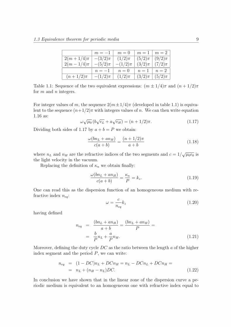
1.3 Equivalence theorem for periodic media 9
m = −1 m = 0 m = 1 m = 22(m + 1/4)π −(3/2)π (1/2)π (5/2)π (9/2)π2(m− 1/4)π −(5/2)π −(1/2)π (3/2)π (7/2)π
n = −1 n = 0 n = 1 n = 2(n + 1/2)π −(1/2)π (1/2)π (3/2)π (5/2)π
Table 1.1: Sequence of the two equivalent expressions: (m± 1/4)π and (n + 1/2)πfor m and n integers.
For integer values of m, the sequence 2(m±1/4)π (developed in table 1.1) is equiva-lent to the sequence (n+1/2)π with integers values of n. We can then write equation1.16 as:
ω√
µ0 (b√
εL + a√
εH) = (n + 1/2)π. (1.17)
Dividing both sides of 1.17 by a + b = P we obtain:
ω(bnL + anH)
c(a + b)=
(n + 1/2)π
a + b(1.18)
where nL and nH are the refractive indices of the two segments and c = 1/√
µ0ε0 isthe light velocity in the vacuum.
Replacing the definition of κn we obtain finally:
ω(bnL + anH)
c(a + b)=
κn
P= kz. (1.19)
One can read this as the dispersion function of an homogeneous medium with re-fractive index neq:
ω =c
neq
kz (1.20)
having defined
neq =(bnL + anH)
a + b=
(bnL + anH)
P=
=b
PnL +
a
PnH . (1.21)
Moreover, defining the duty cycle DC as the ratio between the length a of the higherindex segment and the period P , we can write:
neq = (1−DC)nL + DCnH = nL −DCnL + DCnH =
= nL + (nH − nL)DC. (1.22)
In conclusion we have shown that in the linear zone of the dispersion curve a pe-riodic medium is equivalent to an homogeneous one with refractive index equal to

10 1. Segmented structures
the average of the two refractive indexes nL and nH weighed by the DC. This de-pendency of the equivalent index with a parameter like the DC is very interestingfrom the technological point of view. The refractive index is, in general, a parameterfixed by the technology and is then very hard to change. The DC, on the contrary,is a parameter fixed by the design of the structure and is then relatively simpleto modify. This then allows to modify easily the equivalent index of the structurewithout changing the fabrication technology.
1.4 Periodically segmented waveguides
Up to now, the considered structure is infinite in the transversal directions xand y. This type of structure has a limited range of applications (lens antireflectioncoatings, for example) but has no interest for integrated optics as the field is notconfined. We will then consider now structures that arrange the periodicity of therefractive index, in the propagation direction, and also allow transversal confine-ment of the field. Two examples of these structures are respectively the periodicallysegmented slab (in the following also denoted as periodic slab) and the periodicallysegmented waveguide (in the following also denoted as periodic waveguide) whosestructures are sketched in figure 1.3. For the periodic slab, the confinement of the
n
LD
sn
P
maxW
LD
sn
P
maxn
Figure 1.3: Representation of a periodic slab (left part of the figure) and of a periodicwaveguide (right part).
field is only in one direction and is guaranteed by the total reflection at the film-substrate interface, while, for the periodic waveguide, confinement occurs in bothtransversal directions.
The electromagnetic field propagating through a periodic slab or waveguide stillobeys the equivalent waveguide theorem. Validity of equation 1.22 also for confinedperiod structures has been confirmed by many publications [12, 13, 14, 15]. Theseresults confirm that for wavelengths far away from a band gap, a periodic waveguideis equivalent to a continuous one with the same width and depth but with refractiveindex equal to:
neq = ns + DC∆nmax (1.23)
1.5 Propagation losses in periodically segmented waveguides 11
where ∆nmax and ns are respectively the maximum and the substrate refractiveindex of the periodic waveguide. The use of periodic waveguides allows then toartificially tune the refractive index of the waveguide without changing dopants ortechnology.
The presence of longitudinal discontinuities in the waveguides, however, alsointroduces propagation losses as the guided mode couples to radiation modes. Thispoint is important and merits to be investigated with some more detail.
1.5 Propagation losses in periodically segmented
waveguides
As just said, it is reasonable to expect that, passing from a continuous waveguideto a periodic one, losses appear and increase for decreasing duty cycle as the fractionof high index material in the period, which allows field confinement, is reduced. Inthe low index zone, the field is not confined and is then coupled to radiation modes.The field then spreads and when it reaches the next higher index piece of waveguideit can not be totally coupled back to the guided mode. The smaller is the guidingsegment with respect to the period, the larger will be then the expected losses.
Amazingly, this explanation turns out to be valid only for duty cycles from 0.5to 1. Further reduction of the duty cycle, in fact, leads to a maximum but thenlosses are again reduced approaching DC = 0. This loss reduction is limited by thepresence of the cutoff wavelength, which limits the possible DC reduction.
This behavior has been confirmed both numerically [16, 14] and experimentally[17, 18]. An explanation of the phenomenon is developed in the following. Theelectromagnetic field in the periodic core can be expressed as a combination of theso called spatial harmonics, i.e. solutions with longitudinal propagation constantgiven by:
β + nG, n = ±0, 1, 2...; G =2π
P. (1.24)
In cover and substrate, only the plane waves with the same longitudinal propagationconstant can contribute to the field structure and only some of them significantlycontribute to the overall field. If the transversal propagation constant of theseplanes waves has a small propagation factor in the transversal direction, the modeis still practically confined. More details on this can be found, for example, in [14].Computational result of propagating losses as a function of DC is shown in figure1.4 for a slab waveguide. The attenuation peak at DC slightly larger than 0.9 is dueto Bragg reflection in the structure. The possibility of having small radiation lossesallows then the use of segmented waveguide as standard component in integratedoptics.

12 1. Segmented structures
Figure 1.4: Field attenuation versus DC in periodic waveguide, from Fogli et al.[14].
1.6 Cutoff properties of periodically segmented
waveguides
A further interesting properties of periodic waveguides concerns the dependenceof the cutoff wavelength on the DC [19]. Cutoff is the condition for which the ef-fective index of the propagating mode becomes equal to the substrate index. Suchcondition implies that the mode is no longer confined but is spread out in the sub-strate. Fixing the transversal index distribution in a continuous waveguide (CWG)the cutoff condition depends only on wavelength.
In order to understand how the characteristics of a periodic waveguide can controlthe cutoff wavelength, we consider the easier case of a periodic slab and then weextend the result in the case of a periodic waveguide.
For a slab waveguide the normalized frequency [20] is defined as:
V = LD2π
λ0
√(n2
max − n2s) (1.25)
where nmax is the maximum refractive index of the slab waveguide, ns is the substraterefractive index and LD is the depth of the waveguide. The expression 1.25 can beused for both the step index [21, 22] and the graded index slab [20]. For the diffusedslab waveguide the only assumption is that the index profile decreases monotonicallyfrom the maximum surface value to the substrate one. At cutoff, the normalizedfrequency V depends only on the asymmetry parameter a [22] defined as:
a =n2
s − n2c
n2max − n2
s
(1.26)
where nc is the cladding refractive index. Assuming nmax > ns > nc, the parametera can vary between 0, for the perfect symmetric structures (ns = nc) and infinity,

1.6 Cutoff properties of periodically segmented waveguides 13
for structures with strong asymmetries (ns 6= nc and ns → nmax). In the case ofintegrated optical devices the cladding is generally air and the structures presentstrong asymmetries. This means that a is almost infinity and for all the devicesof this type the value of V is the same. In particular it is possible to say that thenormalized frequency, at cutoff, is the same for a slab waveguide (CWG, continuouswaveguide) and for a periodic slab (PWG, periodic waveguide):
V cutoffPWG = V cutoff
CWG (1.27)
As a consequence, changing the DC of a periodic waveguide, the cutoff wavelengthis modified too. This is a consequence of the equivalence theorem and of equation1.27. Writing nmax as:
nmax = ns + ∆n (1.28)
and assuming a small index change:
∆n2 ¿ 2ns∆n (1.29)
we obtain: (n2
max − n2s
) ≈ 2ns∆n. (1.30)
Replacing approximation 1.30 in the definition of the normalized frequency 1.25, weobtain the following expression for V 2:
V 2 = L2D
(2π
λ0
)2
(n2max − n2
s) ≈ L2D
(2π
λ0
)2
(2ns∆n). (1.31)
Equation 1.31 can be evaluated in the case of a continuous slab and a periodicslab, taking into account the dispersive behavior in frequency of ns and δn. For thecontinuous slab it holds:
(V cutoffCWG )2 = L2
D
(2π
λCWG
)2
2ns(λCWG)∆n(λCWG) (1.32)
where λCWG is the cutoff wavelength of the continuous slab. For the periodic slabit holds:
(V cutoffPWG )2 = L2
D
(2π
λPWG
)2
2ns(λPWG)∆neq(λPWG) (1.33)
where λPWG is the cutoff wavelength of the periodic slab and ∆neq(λPWG) can beexpressed using the relation of the equivalent waveguide 1.23 as:
∆neq(λPWG) = DC∆n(λPWG). (1.34)
Using 1.34, 1.27, 1.32 and 1.33 we can write:
λ2PWGns(λCWG)∆n(λCWG)
λ2CWGns(λPWG)∆n(λPWG)
= DC. (1.35)
14 1. Segmented structures
The terms ns(λCWG)/ns(λPWG) and ∆n(λCWG)/∆n(λPWG) on the left side of equa-tion 1.35 are related to the dispersive behavior of the materials. Neglecting materialdispersion, equation 1.35 can be simplified to:
DC =λ2
PWG
λ2CWG
. (1.36)
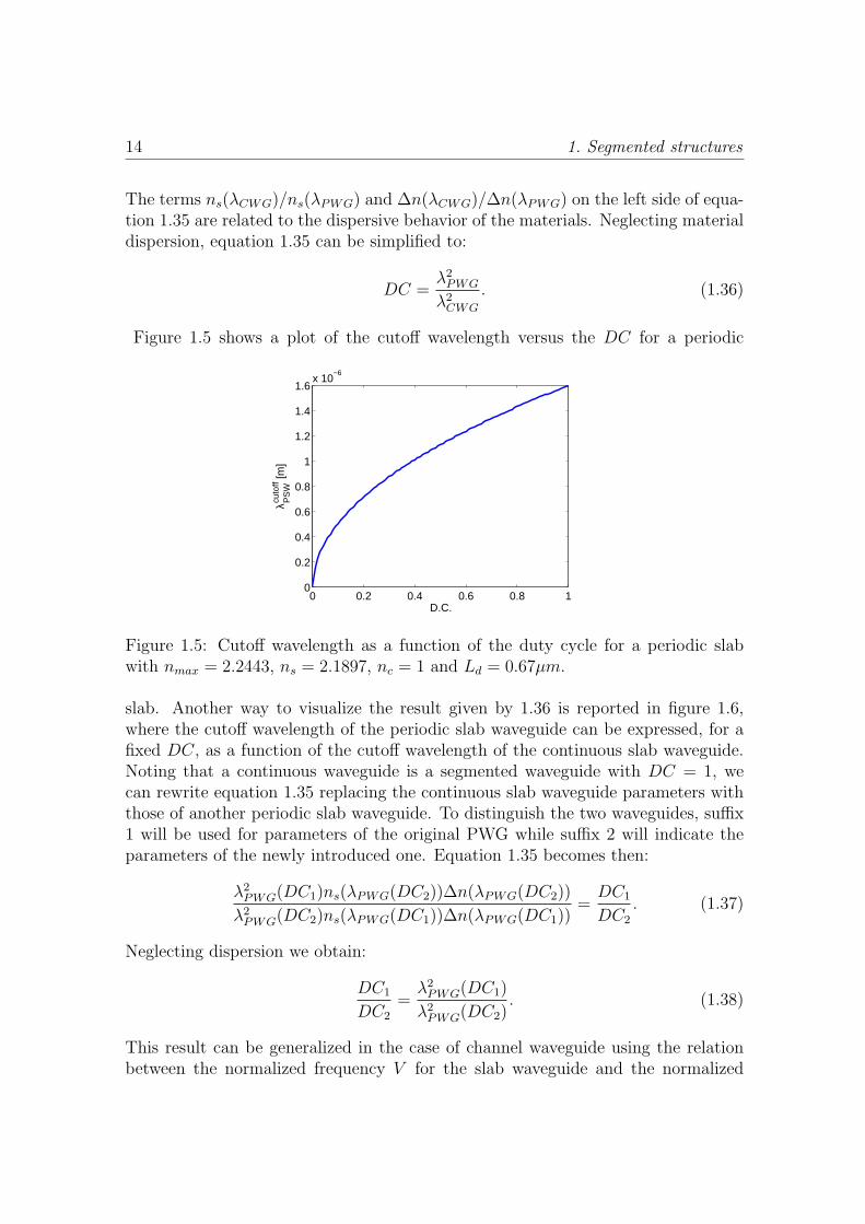
Figure 1.5 shows a plot of the cutoff wavelength versus the DC for a periodic
0 0.2 0.4 0.6 0.8 10
0.2
0.4
0.6
0.8
1
1.2
1.4
1.6x 10
−6
D.C.
λ PS
Wcu
toff [m
]
Figure 1.5: Cutoff wavelength as a function of the duty cycle for a periodic slabwith nmax = 2.2443, ns = 2.1897, nc = 1 and Ld = 0.67µm.
slab. Another way to visualize the result given by 1.36 is reported in figure 1.6,where the cutoff wavelength of the periodic slab waveguide can be expressed, for afixed DC, as a function of the cutoff wavelength of the continuous slab waveguide.Noting that a continuous waveguide is a segmented waveguide with DC = 1, wecan rewrite equation 1.35 replacing the continuous slab waveguide parameters withthose of another periodic slab waveguide. To distinguish the two waveguides, suffix1 will be used for parameters of the original PWG while suffix 2 will indicate theparameters of the newly introduced one. Equation 1.35 becomes then:
λ2PWG(DC1)ns(λPWG(DC2))∆n(λPWG(DC2))
λ2PWG(DC2)ns(λPWG(DC1))∆n(λPWG(DC1))
=DC1
DC2
. (1.37)
Neglecting dispersion we obtain:
DC1
DC2
=λ2
PWG(DC1)
λ2PWG(DC2)
. (1.38)
This result can be generalized in the case of channel waveguide using the relationbetween the normalized frequency V for the slab waveguide and the normalized

1.7 Segmented waveguides 15
0.8 0.9 1 1.1 1.2 1.3 1.4 1.5 1.6
x 10−6
5
6
7
8
9
10
11
12x 10
−7
λcontcutoff
λ PS
Wcu
toff
Figure 1.6: Periodic waveguide cutoff wavelength versus the cutoff wavelength of acontinuous waveguide for a fixed DC equal to 0.55.
frequency V c for a channel waveguide [23].
V c = V bW
LD
(1.39)
where W is the width of the channel waveguide and b is the normalized propagationconstant [23]. Equation 1.39 suggests that for a channel waveguide with fixed widthand depth, the parameter V c is a function of only V and b. Being b a function of Vit is then possible to deduce that V c is directly related to V . At cutoff, V c is thenthe same for a periodic and a continuous waveguide. All the results obtained forslab waveguides can then be extended to channel waveguides.
1.7 Segmented waveguides
Up to now, we have discussed the properties of periodically segmented wave-guides. It is anyway possible to imagine to vary longitudinally any of the parametersdescribing one of the features of the periodic waveguide: the period P , the duty cycleDC and also the lateral width of the pieces of waveguides forming the structure. Inthis case only numerical approaches can be used to determine the electromagneticbehavior of these structures as the propagation constant β is no longer constant, butvaries with z and the ansatz E(x, y, z) = E(x, y) e−jβz cannot be set to determinethe modes of the structure.
It is anyway possible to assume that, locally, the guided field is the same for botha structure with longitudinal features equal anywhere and those of the consideredsection. This is not rigorous, but it is anyway useful, mainly when longitudinal

16 1. Segmented structures
changes are “slow” with respect to the wavelength, so that one can suppose thatthere are no significant changes in the propagation constant or important reflections[24]. We will refer to this structures simply denoting them as segmented .
This conceptually simple extension opens a lot of possibilities to imagine newtypes of structures, but also sets the huge problem of designing a structure optimiz-ing many parameters at the same time. This task can in effect be tackled only ina two step process: the former conceiving the structure with the desired propertiesusing simple, also analytical, approaches; the latter refining the design using 2Dor 3D numerical methods, and, in case, iterating the process until the desired de-vice performances are envisaged. This allows to minimize the number of prototypeswhich must be fabricated. This was in effect the way of working used in this work.
Before entering into detailed descriptions of the realized devices, it is anywayworthwhile provide a brief summary of the most important applications of (peri-odically) segmented structures in optical transmission systems and then provide ageneral description of the problems to be solved by this kind of devices.
Segmented waveguides have been widely used both for linear and non linearapplications such as Bragg reflectors, dispersion compensators, sensors, wavelengthconverters, frequency generation, etc. More details and references can anyway befound in many text books or papers, such as, for example [25, 26, 27, 28, 29, 30, 31].
We now focus our attention to the two particular examples which will have beendeeply investigated in this thesis work. They operate in the almost linear part of thedispersion characteristic (figure 1.2) and then do not present any Bragg reflectioneffect. This way, the use of the local mode approximation will be allowed.
1.7.1 Mode transformers: Taper
The mode transformers or tapers are devices able to couple two different opticalwaveguides allowing maximum energy transfer. Coupling two different waveguides,in fact, induces losses which can be very important. The first cause of loss is relatedto Fresnel reflections, due to the refractive index mismatch of the two waveguides.The second contribution to the coupling losses is related to the different mode shapein the two structures. If the two modes are different, continuity conditions at theinterface induce coupling also to the radiating modes or to higher order modes, ifthey exist. This introduces losses as well.
Fresnel losses can be reduced using proper index matching materials.To minimize shape mismatch losses, a mode transformer should be placed (as
schematically shown in figure 1.7) between the two structures to be coupled, A and B.The three goals of a taper are: reduction of the interface reflections, improvement ofthe mode overlap at the interfaces and reduction of the mode transformation losses.The most interesting application of the taper is coupling optimization between anintegrated optical waveguide and an external optical fiber as these two guides havelarge structural differences. In these cases the presence of a taper between waveguide

1.7 Segmented waveguides 17
?A B
Taper
Figure 1.7: Schematic of the taper insertion between two different optical structures.
and fiber turns out favorable.In order to realize a taper, different solutions can be envisaged, depending on
the specific requirements and the available technology. The first idea that can beproposed in order to increase the propagating mode size in a waveguide is based ona gradual increase of the waveguide size. An example of this type of structure isshown in figure 1.8. The advantage of this kind of taper is the fabrication simplicity.
Core of the fibreWaveguide
Figure 1.8: Schematic representation of a taper obtained by increasing the width ofthe waveguide in the propagation direction.
But a taper of this type it affected by some problems. First of all it is not alwaystrue that increasing the size of an optical waveguide also induces an increase of theguided mode size. Two phenomena exist, in fact, when the dimension of a waveguideis increased. The first phenomenon is the increase of the mode size related to thefact that the guiding structure is larger, the second is the increase of the effectiveindex of the mode, that induces, on the contrary, a better confinement of the field.
The presence of these two effects has the consequence that the mode size cannot change monotonically with the waveguide dimension, but shows a minimumas sketched in figure 1.9. For a fixed fabrication technology an optical waveguidecan be on the left or on the right of the characteristic curve minimum. Increasingthe waveguide section when the initial operating condition is on the right of theminimum means in effect an increase of the mode size. But, if the initial operating

18 1. Segmented structures
condition belongs to the left part of the curve, the increase of the waveguide sizecauses an unwanted reduction of the mode size.
0 2 4 6 8 100
2
4
6
8
10
12
Waveguide width [µm]
Mod
e w
idth
[µm
]
Cut
−of
f
Figure 1.9: Representation of the fundamental mode width in a generic opticalwaveguide as a function of the waveguide width (continuous line) resulting on thecontribution of the effective index (dashed line) and waveguide size (dotted line).
Another problem that occurs in this type of taper is that often, it is not techno-logically easy or even possible to modify the waveguide depth. This causes a strongellipticity of the waveguide mode resulting completely unsatisfactory from the pointof view of the overlap with the fundamental mode of a circular fiber. The last draw-back of this solution is that increasing the waveguide size at a fixed wavelength thestructure can become multimode, which is a condition obviously to be avoided.
A second kind of taper is shown in figure 1.10. A reduction of the waveguidesize can in fact induce a mode size increase as suggested in figure 1.9.
Core of the fibreWaveguide
Figure 1.10: Schematic representation of a taper obtained reducing the width ofthe waveguide in the propagation direction. The mode size widens approaching thecutoff condition.
Reducing the size of the waveguide, in fact, induces a reduction of the effectiveindex and, as a consequence, the mode turns out to be less confined. The advantages

1.7 Segmented waveguides 19
of this type of taper are due to the fact that an increase of both the lateral andvertical mode size can be obtained and that the structure can not become multimode.The drawback are related to technological problems. The only parameter which canbe easily controlled during fabrication is the width of the waveguide and this is theonly parameter which can be used to modify the mode size in both directions. Thismakes the design of this taper critical. Moreover curves at the left of the minimumof figure 1.9 are usually very steep as operating conditions approach cutoff. Thismeans that a small imprecision on the determination of the width of the taper cancause large changes of the mode size.
In this work we have investigated the possibility to use segmented waveguides[32] to provide a third way to fabricate tapers. Expected advantages are fabricationsimplicity and the possibility to eliminate the problems evidenced for the previouslydescribed structures [33].
Core of the fibreWaveguide
Figure 1.11: Schematic representation of a segmented waveguide taper obtainedwith a graded variation of the DC in the propagation direction.
The structure of this segmented waveguide taper is shown in figure 1.11. Thecontinuous waveguide becomes segmented with variable duty cycle along the prop-agation direction. Once reached the desired duty cycle the mode can be stabilizedwith a periodically segmented waveguide. From the equivalent waveguide theoremthis structure can be analyzed as a continuous waveguide with refractive index grad-ually reduced along the longitudinal direction. As a result the mode size is thereforeincreased both in width and depth. The final mode shape depends on the combina-tion of the final duty cycle and the waveguide width. The possibility of controllingthe mode size through two independents parameters is an important features whichprovide less critical design of the structures, with respect to the previously presentedsolutions. Moreover, no unwanted higher order modes appear as segmentation re-duces the effective index with respect to that of the continuous waveguide.
1.7.2 Mode filters
A mode filter is a device able to eliminate one or more higher order modespropagating in a multimode waveguide. Such operation turns out to be particularlyimportant in non linear applications, for example in wavelength conversion. In

20 1. Segmented structures
the case of a difference-frequency mixer, for example, a pump at frequency ωp ismixed with a signal with frequency ωs in order to generate an idler frequency ωi =ωp−ωs. This type of interaction is used in many applications, from the generation ofparticular radiation in the near infrared, to wavelength conversion for WDM systemsor for single photon generation in quantum communication applications. Usuallyidler or signal radiations have wavelength significantly larger with respect to thatof the pump. Even if the guide is monomode at the idler and signal wavelengths,it is multimode at the pump frequency. Therefore, it turns out difficult to couplein efficient way the laser radiation of the pump to the fundamental mode of thewaveguide. Moreover, the unavoidable excitation of higher order modes generatesundesired peaks in the fluorescence output spectrum.
Using segmented waveguides it is possible to solve also this problem. Higherorder modes at the pump wavelength can in fact be filtered by simply reducing thevalue of the duty cycle DC of a segmented waveguide thus leading those modes tocutoff. This is shown in figure 1.12 where the effective indices of the propagatingmodes in the segmented waveguide are reported as a function of DC.
0.2 0.4 0.6 0.8 1
2.179
2.181
2.183
2.185
2.187
2.189
DC
neff
Figure 1.12: Effective index values of guided modes as a function of the DC. Thesubstrate refractive index is ns = 2.1788 (dashed line), for effective index neff
smaller than ns the corresponding mode is at cutoff.
The waveguide considered in this example guides five modes at λp = 775 nm.Reducing DC, the value of their effective indices is reduced. For values of the DCbetween 0.2 and 0.4 just one mode results in propagation (neff > ns). Takingadvantage of this property, a segmented waveguide structure acting as mode filterhas been proposed [34]. A schematization of this solution is shown in figure 1.13.
The input section is a segmented waveguide with constant DC determined to
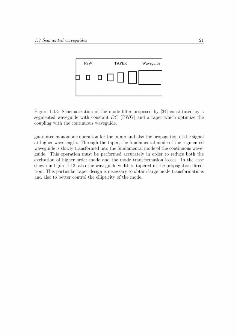
1.7 Segmented waveguides 21
TAPER WaveguidePSW
Figure 1.13: Schematization of the mode filter proposed by [34] constituted by asegmented waveguide with constant DC (PWG) and a taper which optimize thecoupling with the continuous waveguide.
guarantee monomode operation for the pump and also the propagation of the signalat higher wavelength. Through the taper, the fundamental mode of the segmentedwaveguide is slowly transformed into the fundamental mode of the continuous wave-guide. This operation must be performed accurately in order to reduce both theexcitation of higher order mode and the mode transformation losses. In the caseshown in figure 1.13, also the waveguide width is tapered in the propagation direc-tion. This particular taper design is necessary to obtain large mode transformationsand also to better control the ellipticity of the mode.

22 1. Segmented structures

2
Numerical methods
2.1 Introduction
In this chapter the main features of two numerical tools used both to design thecomponents and analyze the experimental results comparing them with theoreticalpredictions will be discussed. The two algorithms solve the fundamental problemsone faces when designing a component: computing both the field evolution along alongitudinally varying guide and the field which can be guided by a longitudinallyinvariant structure. From the mathematical point of view, the former is an initialvalue problem, while the latter is a boundary value problem.
The development of the source code allows to control in detail all the modellingparameters for the different devices. The choice to develop original versions of thecodes instead of buying commercial ones is due to the fact that in this way we havethe full control of all the introduced assumptions and a precise knowledge of thetheoretical and numerical limitations.
The first technique is the so called full vectorial Finite Difference 3D BeamPropagation Method (FD-BPM)[35]. It uses a finite difference scheme to solve theHelmholtz equations in the case of unidirectional propagation of the electromagneticfield trough the optical structure. The formulation originally adopted and extendedfor this work is based on the Helmholtz equations written for the electric field.However, numerical instability problems affecting this kind of solver have been found.To eliminate them, a 3D BPM based on the so called magnetic formulation was thendeveloped. It solves the Helmholtz equation written for the magnetic field. In orderto improve the result accuracy and to allow the study of wide-angle propagations,the paraxial approximation has been replaced by the Pade approximants in bothcodes. The anisotropic Perfectly Matched Layer (PML) boundary condition [36]essential to absorb outgoing radiation was also introduced.
The second numerical technique developed and discussed in this chapter allowsto calculate the mode properties (shape, effective index) of z-invariant structures. Itis a Mode Solver and solves the Maxwell equations by a Finite Difference technique

24 2. Numerical methods
in the Frequency Domain (FD-FD). This tool is also used to calculate the initialconditions (input field) of the 3D BPM if a mode of the structure is to be considered.
2.2 3D fully vectorial Beam Propagation Method
The time domain electromagnetic field behavior in a photonic devices is describedby the Maxwell equations and by the costitutive relations of the material. In aCartesian orthogonal reference frame they can be written as:
∇× E(x, y, z, t) = −∂B(x, y, z, t)
∂t(2.1)
∇×H(x, y, z, t) =∂D(x, y, z, t)
∂t+ J(x, y, z, t) (2.2)
∇ ·D(x, y, z, t) = ρ(x, y, z, t) (2.3)
∇ · B(x, y, z, t) = 0 (2.4)
where
• E and H are the electric and magnetic field vectors
• D and B are the electromagnetic and magnetic induction vectors
• J is the source current vector
• ρ is the electric charge density
• ε and µ are the tensors of dielectric permittivity and magnetic permeability.
Electric and magnetic induction vectors can be expressed as:
D(x, y, z, t) = ε(x, y, z, ω,∣∣E∣∣) · E(x, y, z, t) (2.5)
B(x, y, z, t) = µ(x, y, z, ω,∣∣H
∣∣) ·H(x, y, z, t) (2.6)
which set the relations between electromagnetic fields and material properties. Per-mittivity and permeability are represented by tensorial quantities in order to takeinto account anisotropic materials. They depend on the considered point (x, y, z),the frequency (ω) and on the electric and magnetic field intensity. In this way wecan consider non homogeneous materials with both frequency dispersion and nonlinearity. The solution of this completely general problem is not always necessaryand we can then simplify the model according to the characteristics of the consideredstructures.
We can first assume that the tensor µ is a scalar constant:
µ = µ0 = 4π10−7H/m (2.7)
2.2 3D fully vectorial Beam Propagation Method 25
while for the dielectric properties we consider a linear, non dispersive and isotropicmaterial. In this case ε(x, y, z, ω,
∣∣E∣∣) reduces to a scalar function of the point:
ε(x, y, z). We can finally assume also that no charges (ρ = 0) and no sources (J = 0)are present in the computational domain.
For the linearity of Maxwell equations we can consider also a stationary harmonicregime. This allows to introduce complex vectors [37]:
E(x, y, z, t) = <E(x, y, z) ejωt
H(x, y, z, t) = <H(x, y, z) ejωt
where <· denotes the real part of the argument.Introducing all these hypotheses in the Maxwell equations, after some simple
algebra, we get:
∇2E(x, y, z) + k20n
2(x, y, z) E(x, y, z) = ∇ (∇ · E(x, y, z))
(2.8)
where k0 = 2π/λ0 is the wavenumber in vacuum and n(x, y, z) =√
ε(x,y,z)ε0
is the
local refractive index.Being ρ = 0, equation 2.3 reduces to ∇ ·D(x, y, z, t) = 0 and we can write:
∇ ·D(x, y, z) = ∇ · ε(x, y, z)E(x, y, z) =
= ε(x, y, z)∇ · E(x, y, z) +∇ε(x, y, z) · E(x, y, z) =
= 0. (2.9)
From this, it follows immediately that ∇ · E(x, y, z) can be expressed as:
∇ · E(x, y, z) = −∇ε(x, y, z)
ε(x, y, z)· E(x, y, z) =
= −∇n2(x, y, z)
n2(x, y, z)· E(x, y, z). (2.10)
Inserting 2.10 in 2.8 we obtain:
∇2E(x, y, z) + k20n
2(x, y, z)E(x, y, z) = ∇ (∇ (ln n2(x, y, z)
) · E(x, y, z)). (2.11)
This is the Helmholtz vectorial equation. In the adopted Cartesian reference frame,this equation can be separated in tree equations of the type:
∂2Ei(x, y, z)
∂x2+
∂2Ei(x, y, z)
∂y2+
∂2Ei(x, y, z)
∂z2+
+k20n
2(x, y, z)Ei(x, y, z) = − ∂
∂i
[Ex(x, y, z)
∂ ln n2(x, y, z)
∂x+
Ey(x, y, z)∂ ln n2(x, y, z)
∂y+ Ez(x, y, z)
∂ ln n2(x, y, z)
∂z
](2.12)
26 2. Numerical methods
where i can be x, y or z and Ex(x, y, z), Ey(x, y, z), Ez(x, y, z) are the cartesiancomponents of the electric field:
E(x, y, z) = Ex(x, y, z)x + Ey(x, y, z)y + Ez(x, y, z)z. (2.13)
If z is associated to the propagation direction, one can write any component as theproduct of a rapidly varying propagation term (e−jk0n0z) and a slowly varying oneFi(x, y, z), the so called pulse envelope:
Ei(x, y, z) = Fi(x, y, z) e−jk0n0z (2.14)
where n0 is a properly chosen reference refractive index.Replacing 2.14 in 2.12 for i = x we obtain:
∂2Fx(x, y, z)e−jβz
∂x2+
∂2Fx(x, y, z)e−jβz
∂y2+
∂2Fx(x, y, z)e−jβz
∂z2+
+k20n
2(x, y, z)Fx(x, y, z)e−jβz = − ∂
∂x
[Fx(x, y, z)e−jβz ∂ ln n2(x, y, z)
∂x+
Fy(x, y, z)e−jβz ∂ ln n2(x, y, z)
∂y+ Fz(x, y, z)e−jβz ∂ ln n2(x, y, z)
∂z
]
where β = k0n0 is the reference propagation constant. Developing separately thethree derivatives:
∂2Fx(x, y, z)e−jβz
∂x2= e−jβz ∂2Fx(x, y, z)
∂x2
∂2Fx(x, y, z)e−jβz
∂y2= e−jβz ∂2Fx(x, y, z)
∂y2
∂2Fx(x, y, z)e−jβz
∂z2=
∂
∂z
(e−jβz ∂Fx(x, y, z)
∂z− jβFx(x, y, z)e−jβz
)
we obtain:
e−jβz ∂2Fx(x, y, z)
∂x2+ e−jβz ∂2Fx(x, y, z)
∂y2− jβe−jβz ∂Fx(x, y, z)
∂z+
+e−jβz ∂2Fx(x, y, z)
∂z2− jβe−jβz ∂Fx(x, y, z)
∂z+ (−jβ) (−jβ) e−jβzFx(x, y, z) +
+k20n
2(x, y, z)Fx(x, y, z)e−jβz = − ∂
∂x
[Fx(x, y, z)e−jβz ∂ ln n2(x, y, z)
∂x+
+Fy(x, y, z)e−jβz ∂ ln n2(x, y, z)
∂y+ Fz(x, y, z)e−jβz ∂ ln n2(x, y, z)
∂z
].
This equation can be rearranged as:
−∂2Fx(x, y, z)
∂z2+ j2β
∂Fx(x, y, z)
∂z=
∂2Fx(x, y, z)
∂x2+
∂2Fx(x, y, z)
∂y2+

2.2 3D fully vectorial Beam Propagation Method 27
+(k2
0n2 − β2
)Fx(x, y, z) +
∂
∂x
[Fx(x, y, z)
∂ ln n2(x, y, z)
∂x+
+Fy(x, y, z)∂ ln n2(x, y, z)
∂y+ Fz(x, y, z)
∂ ln n2(x, y, z)
∂z
]. (2.15)
If one can assume that the so called Slowly Varying Envelope Approximation(SVEA) ∣∣∣∣
∂2Fx(x, y, z)
∂z2
∣∣∣∣ ¿ 2k0n0
∣∣∣∣∂Fx(x, y, z)
∂z
∣∣∣∣ (2.16)
holds, the contribution of ∂2Fx(x,y,z)∂z2 is negligible in 2.15. This approximation, also
known as paraxial approximation [38], fixes a limit on the variation of field envelopeduring the propagation. If SVEA is a too much restrictive condition, it is possibleto introduce the Pade approximate operators. They allow to better describe wideangle propagation [39, 40, 41]. The code previously developed was then extended toinclude the Pade operators. To do so, we first move all the derivatives of Fx(x, y, z)to the left side of 2.15 in order to leave on the right side only terms which dependon Fy and Fz:
∂2Fx(x, y, z)
∂z2− 2jβ
∂Fx(x, y, z)
∂z+
+∂2Fx(x, y, z)
∂x2+
∂2Fx(x, y, z)
∂y2+
∂
∂x
(Fx(x, y, z)
∂lnn(x, y, z)2
∂x
)+
+(k2
0n2(x, y, z)− β2
)Fx(x, y, z) =
= − ∂
∂x
[Fy(x, y, z)
∂lnn2(x, y, z)
∂y+ Fz(x, y, z)
∂lnn2(x, y, z)
∂z
].
︸ ︷︷ ︸Q
We can then write:
− ∂
∂z
(∂
∂z− 2jβ
)Fx(x, y, z) = PFx(x, y, z) + Q
= P
(1 +
Q
PFx(x, y, z)
)Fx(x, y, z)
which allows to obtain the z-derivative of Fx(x, y, z):
∂Fx(x, y, z)
∂z= −
P(1 + Q
PFx(x,y,z)
)
∂∂z− 2jβ
Fx(x, y, z) =− [P(1+ Q
PFx(x,y,z))]2jβ
12jβ
∂∂z− 1
Fx(x, y, z)
=
−j[P(1+ QPFx(x,y,z))]2β
1 + j2β
∂∂z
Fx(x, y, z). (2.17)

28 2. Numerical methods
From 2.17 we can find the iterative expression of ∂∂z
by using the Pade approximants:
∂
∂z
∣∣∣∣p
=
−j[P(1+ QPFx(x,y,z))]2β
1 + j2β
∂∂z
∣∣p−1
. (2.18)
We have obtained a recursive relation for the operator ∂·∂z
whose precision dependson the value of p. Increasing p we obtain a better approximation. For example, ifp = 1 we can write:
∂
∂z
∣∣∣∣1
=−jP
(1 + Q
PFx(x,y,z)
)
2β(2.19)
while for p = 2 we find:
∂
∂z
∣∣∣∣2
=
−j[P(1+ QPFx(x,y,z))]2β
1 + j2β
∂∂z
∣∣1
=
−j[P(1+ QPFx(x,y,z))]2β
1 + j2β
−jP(1+ QPFx(x,y,z))2β
=
−j[P(1+ QPFx(x,y,z))]2β
1 +P(1+ Q
PFx(x,y,z))4β2
. (2.20)
Usually, we refer to these two examples as Pade approximants of order (1, 0) and(1, 1) respectively. The first number is the degree of the numerator polynomial,while the second one is the degree of the denominator polynomial. Note that forthe approximant (1, 0) we obtain the paraxial approximation obtained eliminatingthe second order derivative term of the field in the propagation direction. We canfinally write equation 2.17 using Pade approximant (1, 1):
∂Fx(x, y, z)
∂z=
−jP(1+ Q
Fx(x,y,z))2β
1 + j2β
−jP(1+ QPFx(x,y,z))2β
= −jN
DFx(x, y, z) (2.21)
where N and D are respectively:
N =P
(1 + Q
PFx(x,y,z)
)
2β
D = 1 +P
(1 + Q
PFx(x,y,z)
)
4β2.
From 2.21 one then gets:
D∂Fx(x, y, z)
∂z= −jNFx(x, y, z).

2.2 3D fully vectorial Beam Propagation Method 29
Repeating the same procedure for Fy and Fz and separating the contribution ofthe different terms, it is possible to rewrite the vectorial equations in the followingcompact formulation:
−∂Fx(x, y, z)
∂z= GxxFx(x, y, z) + GxyFy(x, y, z) + GxzFz(x, y, z)
−∂Fy(x, y, z)
∂z= GyxFx(x, y, z) + GyyFy(x, y, z) + GyzFz(x, y, z) (2.22)
−∂Fz(x, y, z)
∂z= GzxFx(x, y, z) + GzyFy(x, y, z) + GzzFz(x, y, z)
From this system of equations it is quite easy to understand how to move from avectorial to a scalar formulation of the BPM. First of all, just one equation is neededand then all the coupling terms must vanish. In many case a scalar formulation canbe used to find preliminary results in structures where the polarization state ispreserved during the propagation. The main advantage is the reduced memory andtime consuming with respect to a full vectorial formulation.
2.2.1 Finite difference schematization
To solve numerically these equations, a finite difference approach has been adopted:the continuous space is sampled on a lattice structure defined in the computationalregion using a ∆x, ∆y, ∆z mesh and all the differential operators are replaced bytheir corresponding finite-difference ones. This can be done observing that a com-plex function f(x) of a real variable x, which can be derived at x = a, has derivativesin this point equal to:
f ′(a) = limh→0
f(a + h)− f(a)
h. (2.23)
This derivative can be approximated by a central difference scheme as:
f ′(a) ∼= f(a + h)− f(a− h)
2h. (2.24)
The same procedure can be applied to the second order derivative:
f ′′(a) ∼= f(a + h)− 2f(a) + f(a− h)
h2=
f ′(a + h)− f ′(a− h)
2h. (2.25)
Applying this rules to equations 2.22 the differential problem becomes the followingalgebraic one:
[A] · x = b (2.26)
where [A] is the coefficient matrix, b is the known terms vector and x is the unknownvector.

30 2. Numerical methods
2.2.2 Crank-Nicholson method
As said before, BPM is an initial value problem. Once the initial conditions areset, the evolution of the propagating field can be calculated. In particular, from theknowledge of the field envelope Fi in a section l (in the following F l
i ) the algorithmcalculates Fi in the following section l + 1 (in the following F l+1
i ). The choice ofthe differential scheme is important because it affects both the stability and theperformance of the algorithm. Considering, for example, the equation at the partialderivatives:
∂f(x, y, z)
∂z= a1
∂g(x, y, z)
∂x+ a2
∂g(x, y, z)
∂y(2.27)
we can adopt two different methodologies to obtain a numerical solution:
• explicit scheme: the solution is obtained approximating 2.27 with:
f l+1(x,y,z) − f l
(x,y,z)
∆z= a1
gl(x+∆x,y,z) − gl
(x,y,z)
∆x+ a2
gl(x,y+∆y,z) − gl
(x,y,z)
∆y. (2.28)
In this case f l+1(x,y,z) can be directly calculated knowing the complete distribu-
tion of the two functions f(x, y, z) and g(x, y, z) at the previous step l. Theapproach is very simple to implement, but there are some constraint whichmust be satisfied to guarantee that the algorithm is stable [42].
• implicit scheme:
f l+1(x,y,z) − f l
(x,y,z)
∆z=
1
2
a1
gl+1(x+∆x,y,z) − gl+1
(x,y,z)
∆x+ a2
gl+1(x,y+∆y,z) − gl+1
(x,y,z)
∆y+
+a3gl(x+∆x,y,z) − gl
(x,y,z)
∆x+ a4
gl(x,y+∆y,z) − gl
(x,y,z)
∆y
.
(2.29)
In this case, the solution is more complicated because there are more unknownsat the l +1 step which are related each other. The advantage of this approachis that this solution is always stable for all the values of ∆z [43, 44, 42].
Our BPM solves the equivalent problem 2.27 modifying the Crank-Nicholson method[45], which is one of the most popular implicit finite difference numerical schemes.This method allows to write equation 2.29 in this way:
f l+1(x,y,z) − f l
(x,y,z)
∆z= α
a1
gl+1(x+∆x,y,z) − gl+1
(x,y,z)
∆x+ a2
gl+1(x,y+∆y,z) − gl+1
(x,y,z)
∆y+
l+1
+(1− α)
a3
gl(x+∆x,y,z) − gl
(x,y,z)
∆x+ a4
gl(x,y+∆y,z) − gl
(x,y,z)
∆y
l

2.2 3D fully vectorial Beam Propagation Method 31
where α is a weighting factor necessary to stabilize the whole system. From thenumerical point of view, the possible values of α can change from 0.5, which allowsvery precise solution but causes instability in some cases, to 1 where a numericalattenuation is introduced perturbing the result but assuring algorithm stability [46].
We followed a mixed approach, in which the explicit scheme was used to evaluatethe coupling terms of 2.22 and the implicit scheme was used for the other terms. Atthe point x = h, y = p one can then write:
(−∂Fx(x, y, z)
∂z
)
h,p
∼= F l+1x
(h, p)− F lx(h, p)
∆z. (2.30)
The coupling terms GxyFy and GxzFz are developed at l step with the explicit schemewhile the term GxxFx is written using the implicit one. The stability is provided bythe α parameter. After some algebra, the final system turns out to be:
A1(h, p)F l+1x
(h + 1, p) + A2(h, p)F l+1x
(h− 1, p)+
A3(h, p)F l+1x
(h, p + 1) + A4(h, p)F l+1x
(h, p− 1)+
A5(h, p)F l+1x
(h, p) = Nx(h, p)
(2.31)
C1(h, p)F l+1y
(h + 1, p) + C2(h, p)F l+1y
(h− 1, p)+
C3(h, p)F l+1y
(h, p + 1) + C4(h, p)F l+1y (h, p− 1)+
C5(h, p)F l+1y
(h, p) = Ny(h, p)
(2.32)
G1(h, p)F l+1z
(h + 1, p) + G2(h, p)F l+1z (h− 1, p)+
G3(h, p)F l+1z
(h, p + 1) + G4(h, p)F l+1z (h, p− 1)+
G5(h, p)F l+1z
(h, p) = Nz(h, p)
(2.33)
The solution of this system can be obtained using iterative methods [47], in partic-ular for our BPM we have adopted a GMRES solver.
2.2.3 Perfect Matched Layer
The equations described so far hold in an infinite domain, corresponding to thetransversal section. Their numerical implementation requires that they are limitedto the finite computational domain. Proper boundary conditions must then be set inorder to simulate in the mathematical model the infinite physical domain. Differentapproaches have been proposed so far. Absorbing Boundary Conditions (ABC)[46], which use an artificial layer on the boundary to absorb the incident field, andTransparent Boundary Conditions (TBC) [48], which simulate the infinite domainmaking some assumption on the characteristics of the incident field, have been used
32 2. Numerical methods
to reduce field refections but with non satisfactory results. The introduction ofanisotropic absorbing layers called Perfectly Matched Layers (PML) [49, 36] hasefficiently eliminated the field reflection at computational windows. The idea ofBerenger, who first proposed the PML to absorb outgoing radiation [49], was todivide the magnetic field component Hz into two subcomponents Hzx and Hzy andto operate on them so that the interface between PML and free space could resultrefectionless for all wavelengths, polarizations and incident angles.
Later on, Sacks [50] used the anisotropic material properties (ε, µ, σE, σH) todescribe the absorbing PML layer, where σE and σH are the electric and magneticconductibility, respectively. Let us then consider a material with complex diagonalrelative permittivity and permeability tensors given by
εr =
εxr +
σxE
jω0 0
0 εyr +
σyE
jω0
0 0 εyr +
σyE
jω
µr =
µxr +
σxH
jω0 0
0 µyr +
σyH
jω0
0 0 µyr +
σyH
jω
.
(2.34)
In order to match the intrinsic impedance of the free space, the condition
ε0εr
ε0
=µ0µr
µ0
(2.35)
must be satisfied. Therefore it must be:
εr = µr =
a 0 00 b 00 0 c
= Λ (2.36)
where
a = εxr +
σxE
jω= µx
r +σx
H
jω
b = εyr +
σyE
jω= µy
r +σy
H
jω
c = εzr +
σzE
jω= µz
r +σz
H
jω.
By studying the reflection coefficients at the interfaces between the PML region andfree space, we find that in certain circumstances reflection can be zero. For the PML
region with an interface where x = const and y = const, Λ is required to be [51]:
Λx =
a 0 00 1
a0
0 0 1a
(2.37)

2.2 3D fully vectorial Beam Propagation Method 33
for x = const, and
Λy =
1b
0 00 b 00 0 1
b
(2.38)
for y = const. Fhe PML tensor is obtained multiplying the previous two tensors forthe PML regions at the four corners of the computational window:
Λxy = Λx · Λy =
ab
0 00 b
a0
0 0 1ab
. (2.39)
For the full-vectorial formulation we then modify the permittivity and perme-ability tensors ε and µ to
ε = ε · S−1
µ = µ · S (2.40)
where
S =
SySz
Sx0 0
0 SzSx
Sy0
0 0 SxSy
Sz
. (2.41)
The PML parameters (Sx, Sy, Sz) are assigned to each PML region as shown in figure
2.1: for the non-PML regions, the PML tensor S is an identity matrix, while in thePML regions the parameters are given by:
Si = 1− jσMAX
E
ωε0εPMLr
(ρ
di
)m
, i = 1, 2, 3, 4 (2.42)
where ρ is the distance from the PML boundary, d is the thickness of the PML layerand m controls the profile of the conductivity. Generally, linear (m = 1), parabolic(m = 2) and cubic (m = 3) conductivity profiles are assumed. The maximumelectric conductivity σMAX
E and the permittivity of the PML layers are determinedfrom the required reflection coefficient [52] according to [53]:
Ri = exp
(− 2σmax
E di
3ε0c√
εPMLr
)(2.43)
where Ri is the reflection coefficient of the ith PML region and c is the light velocityin vacuum. Typically Ri is chosen to be about 10e− 4 [53] and σMAX
E to be about0.01Ω−1(µm)−1 when the permittivity is chosen as 1. The parameters (Sx, Sy, Sz)are still all equal to 1 for non-PML regions and assigned according to figure 2.1 for

34 2. Numerical methods
1 2
3
4
5 6
7 8
(s1,s3,1) (s2,s3,1)
(s2,s4,1)
(s2,1,1)
(s1,s4,1)
(s1,1,1)
(1,s4,1)
(1,s3,1)
(1,1,1)
d1 d2
d3
d4
Figure 2.1: Computational domain surrounded by perfectly matched layer (PML).
PML regions. Note that the transformations set by equation 2.40 are intrinsicallyequivalent to modify the ∇ operator of 2.11 into
∇ = x Sx∂
∂x+ y Sy
∂
∂y+ z Sz
∂
∂z. (2.44)
However, this does not introduce extra programming complexity, since all the pro-cedures related to the iterative solver and propagation technique remain unchanged.
2.2.4 BPM validation
Two kinds of validation for the 3D BPM algorithm will be discussed: the effectof PML and the effect of Pade approximants.
To test the efficiency of the PML absorber, we calculate first Gaussian beampropagation in the free space with and without absorbing layers. Then we comparethese two results with the correct field obtained adopting a larger computationalwindow, chosen to avoid interactions between field and domain boundary. Figure2.2 shows Gaussian beam propagation in the free-space when boundary conditionare absent. The input beam is launched on the (x, y)-plane. As expected, the beamis reflected when approaching the computational boundary and after some distancethe reflection strongly interferes with the original propagating beam. The totalpower within the computational window is conserved. Errors are large, as it can beobserved in the last figure of the sequence.
These results can be compared with those obtained when the free space is sur-rounded by the anisotropic PML absorber. At the interface between PML and freespace, reflection is completely eliminated, as clearly shown in figure 2.3. In this cal-culation, the transversal mesh size is given by ∆x = ∆y = 0.2 µm, the propagation

2.2 3D fully vectorial Beam Propagation Method 35
Figure 2.2: From upper left to lower right: gaussian beam intensity at z = 0,z = 4 µm, z = 8 µm, z = 12 µm, z = 16 µm, z = 20 µm (Without PML).
step is ∆z = 0.1 µm, and the conductivity distribution inside the PML region has aparabolic profile.
Figure 2.3: From upper left to lower right: gaussian beam intensity at z = 0,z = 4 µm, z = 8 µm, z = 12 µm, z = 16 µm, z = 20 µm (With PML).
36 2. Numerical methods
Looking at the figures, the field does not seem perturbed by the presence ofthe PML layers. To check quantitatively this qualitative result, a simulation with abigger computational windows has been made. In the left part of figure 2.4, a sectionof the four field profiles (y = 35 µm) calculated at the same plane of z = 20 µm isplotted. The dashed line refers to the field computed in a 70 µm× 70 µm window;the black line refers to the field computed in a 40 µm×40 µm window with 20 PMLlayers; the red line refers to the field computed in a 40 µm×40 µm window withoutPML. The oscillations due to reflections when PML are not used appear clearly,while the field distribution obtained using PML practically superimpose to the fieldcomputed in the larger domain, thus proving the ability of PML to simulate aninfinite computational domain. The right part of figure 2.4 shows differences amongthe results in terms of relative error between the results obtained in the smallercomputational window and those obtained in the larger one. In the PML case theerror is of the order of 10−4 and in the figure it almost coincides with the x-axis.
0 1 2 3 4 5 6 7
x 10−5
0
1
2
3
4
5
6
7x 10
6
x [m]
Inte
nsity
[a.u
.]
Big domainPMLno−PML
Free space PML
0 1 2 3 4 5 6 7
x 10−5
0
0.2
0.4
0.6
0.8
1
x [m]
Rel
ativ
e er
ror
PMLno−PML
Free space PML
Figure 2.4: In the left part we show the field section at z = 20 µm calculated withPML (black line) and without PML (red line) compared with the numerical resultobtained for a large computational window (dashed line). In the right part we showthe relative error for the PML and non-PML solution respect the case of big domain.
To confirm absorption in the PML layers, figure 2.5 shows the evolution of thetotal power in the computational domain during propagation. Power reductioncaused during the propagation by the artificial loss of the PML is evident. Fromthe physical point of view this power reduction corresponds to the power radiatedoutside the computational window.
The second kind of test we have done concern the effect of the Pade approxi-mant introduction. To do that we consider a tilted gaussian beam propagation infree space and we compare the two solutions obtained with the paraxial approxi-mation and with Pade (1,1) with respect to the theoretical field obtained Fouriertransforming the initial beam. The calculation domain is the same adopted for thePML validation.
2.2 3D fully vectorial Beam Propagation Method 37
0 0.5 1 1.5 2 2.5
x 10−5
7
7.5
8
8.5
9
9.5
10
z [m]
Pow
er [W
]
PMLno−PML
Figure 2.5: Power in the computational window at different propagation steps: con-stant when PML are not used, decreasing when PML are used.
−2 −1 0 1 2
x 10−5
0
0.2
0.4
0.6
0.8
1
X [m]
Nor
mal
ized
inte
nsity
z = 4 µm, θ=10o
Exciting fieldTheoretical solutionBPM:PadéBPM:Paraxial app.
Figure 2.6: Comparison between the solutions obtained with the paraxial approxi-mation and with Pade (1,1) with respect to the theoretical field for a tilted gaussianpropagation in free space at 10.
Figure 2.6 shows the results for a propagation angle of 10. As one can see onlyresults obtained using the Pade approximants agree quite well with the expectedfield shape, while this does not happen when the paraxial approximation is used.For larger angles, an higher approximation order with respect to (1,1) is howevernecessary.

38 2. Numerical methods
2.2.5 Consideration on the non-unitarity of BPM operators
While numerous numerical simulations of optical devices have been performedwith explicitly stable one-way scalar finite-difference electrical field propagationmethods, electric field polarization evolution in complex waveguiding geometriesmust be described using the full vectorial finite-element procedures. However, thesealgorithms intrinsically violate power-conservation [54]. This is due to numericalproblems induced in difference calculations by the discontinuities of some of theelectric field components at the interfaces between different dielectric materials. Tosolve this problem we have implemented also a formulation of the fully vectorialBPM with PML and Pade (1,1) based on the vector Helmholtz equations writtenfor the magnetic field instead of the electric field:
∇2H + n20k
20H +
1
n20
∇n20 ×
(∇×H)
= 0 (2.45)
using the condition:
∇ ·H = 0. (2.46)
The magnetic field distribution does not present any discontinuity at dielectric in-terfaces. With this approach stable solutions has been obtained even in cases wherethe E formulation fails. The formal steps necessary to develop the equation to besolved, formally similar to 2.31, 2.32, 2.33, starting from the Helmholtz equation arepractically the same used for the E field formulation developed in the last section,and will then not reported, for the sake of brevity.
Figure 2.7 shows the computed fields propagating in a square waveguide (n = 1.1)surrounded by air using both the E and H formulation. Note that for the electric fieldcomponents Ex and Ey discontinuities appear at the interfaces between waveguideand air in x and y direction, respectively, while the magnetic field is not affected bythese discontinuities.
2.3 Finite difference mode solver
A further code developed and used during this thesis allows to calculate themodes propagating in a z-invariant structure. In this case just one section of thestructure must be studied, as the ansatz of separation of variables can be doneand the field propagating along z is assume to depend on such a coordinate by thetranslation factor (exp (−jβz)).
To implement our mode solver we have adopted the formulation proposed by [55].The structure is superimposed to a cartesian mesh with not necessarily constantsteps. The general case, for an arbitrary point P inside the mesh with neighboringpoints N,W,S,E is shown in figure 2.8. The used Helmholtz equations follows the H

2.3 Finite difference mode solver 39
Figure 2.7: Six components of the fundamental mode of a square waveguide withrefractive index 1.1 surrounded by air calculated with both the E (left) and H (right)BPM formulations.
scheme for the four subregions (ν = 1, 2, 3, 4):
∂2Hx
∂x2+
∂2Hx
∂y2+
(ενk
2 − β2)Hx = 0 (2.47)
∂2Hy
∂x2+
∂2Hy
∂y2+
(ενk
2 − β2)Hy = 0 (2.48)

40 2. Numerical methods
N
PW
S
Ee2
e3 e4
e1
Dx+Dx
-
Dy+
Dy-
Figure 2.8: Point P and neighboring points in a cartesian mesh with uniform dielec-tric constant ε1, ε2, ε3, ε4 of the subregion 1-4.
To obtain the discrete formulation, the differential operators can be developed usinga second order Taylor expansion:
HW = HP −∆x−∂H
∂x
∣∣∣∣W
+(∆x−)
2
2
∂2H
∂x2
∣∣∣∣W
+ O[(
∆x−)3
](2.49)
HE = HP + ∆x+ ∂H
∂x
∣∣∣∣E
+(∆x+)
2
2
∂2H
∂x2
∣∣∣∣E
+ O[(
∆x+)3
](2.50)
HS = HP −∆y−∂H
∂y
∣∣∣∣W
+(∆y−)
2
2
∂2H
∂y2
∣∣∣∣W
+ O[(
∆y−)3
](2.51)
HN = HP + ∆y+ ∂H
∂y
∣∣∣∣N
+(∆y+)
2
2
∂2H
∂y2
∣∣∣∣N
+ O[(
∆y+)3
](2.52)
The possibility of choosing different values for ∆x± and ∆y± allows to reduce themesh step where the field is expected to concentrate, but should be done with care,as it also influences precision, which decreases for increasing mesh size differences.
The approximated expression for the second order derivative operators can beobtained adding the equation 2.49 to 2.52, 2.49 to 2.51, 2.50 to 2.51 and 2.50 to 2.52respectively. Replacing the operators in the Helmholtz equations we obtain:
2HW
(∆x−)2 −2HP
(∆x−)2 +2
∆x−∂H
∂x
∣∣∣∣W
+
+2HN
(∆y+)2 −2HP
(∆y+)2 −2
∆y+
∂H
∂y
∣∣∣∣N
+
+(ε2k
2 − β2)HP = 0 (2.53)
2HW
(∆x−)2 −2HP
(∆x−)2 +2
∆x−∂H
∂x
∣∣∣∣W
+
2.3 Finite difference mode solver 41
+2HS
(∆y−)2 −2HP
(∆y−)2 +2
∆y−∂H
∂y
∣∣∣∣S
+
+(ε3k
2 − β2)HP = 0 (2.54)
2HE
(∆x+)2 −2HP
(∆x+)2 −2
∆x+
∂H
∂x
∣∣∣∣E
+
+2HS
(∆y−)2 −2HP
(∆y−)2 +2
∆y−∂H
∂y
∣∣∣∣S
+
+(ε4k
2 − β2)HP = 0 (2.55)
2HE
(∆x+)2 −2HP
(∆x+)2 −2
∆x+
∂H
∂x
∣∣∣∣E
+
+2HN
(∆y+)2 −2HP
(∆y+)2 −2
∆y+
∂H
∂y
∣∣∣∣N
+
+(ε1k
2 − β2)HP = 0 (2.56)
where H stands for Hx or Hy. Applying continuity condition at the boundaries ofneighboring cells we can eliminate the first order derivative component of H. Thiscan be done with the relation ∇ ·H = 0 obtaining:
Hz =1
jβ
(∂Hx
∂x+
∂Hy
∂y
)(2.57)
Ez =1
jεk
õ0
ε0
(∂Hy
∂x+
∂Hx
∂y
). (2.58)
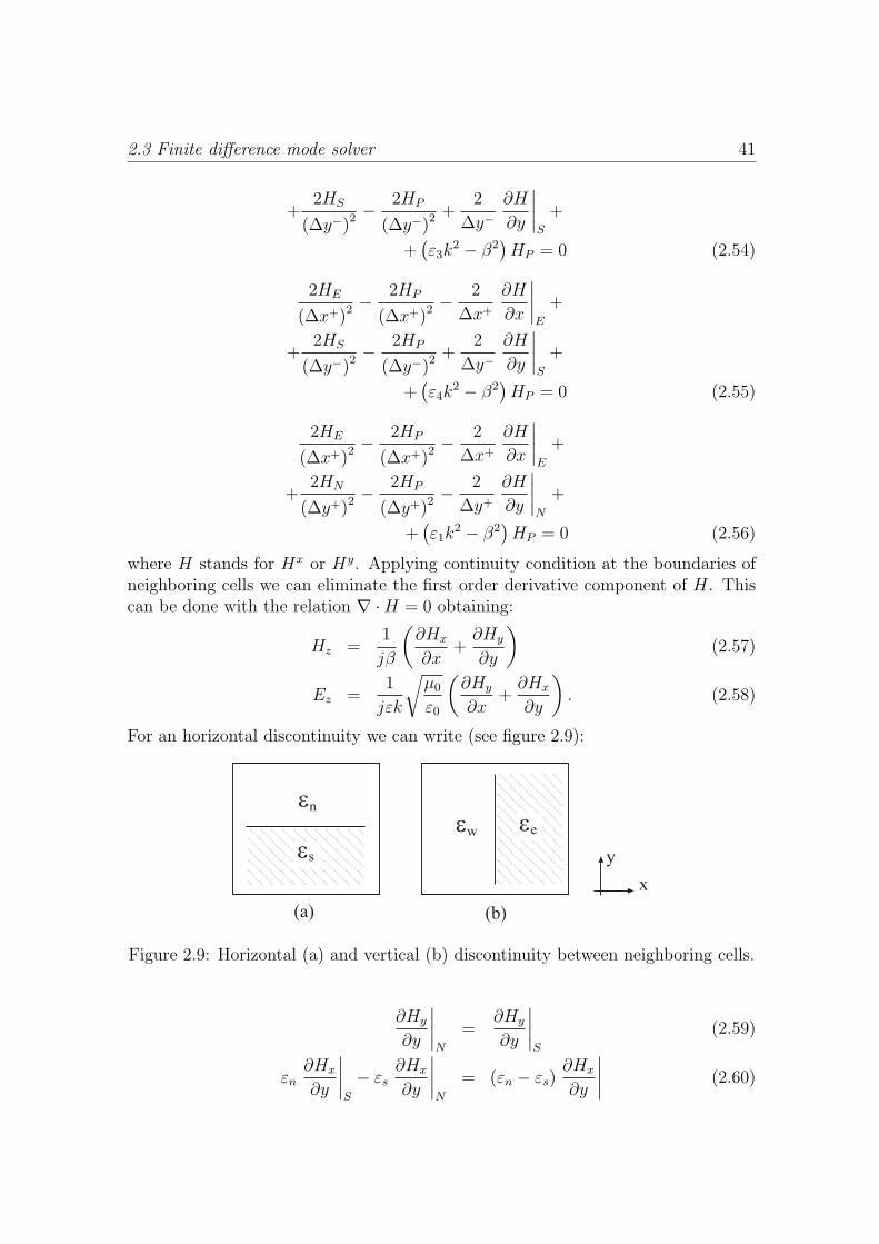
For an horizontal discontinuity we can write (see figure 2.9):
e
es
n
eeew
x
y
(a) (b)
Figure 2.9: Horizontal (a) and vertical (b) discontinuity between neighboring cells.
∂Hy
∂y
∣∣∣∣N
=∂Hy
∂y
∣∣∣∣S
(2.59)
εn∂Hx
∂y
∣∣∣∣S
− εs∂Hx
∂y
∣∣∣∣N
= (εn − εs)∂Hx
∂y
∣∣∣∣ (2.60)

42 2. Numerical methods
while for a vertical one:
∂Hx
∂x
∣∣∣∣W
=∂Hx
∂x
∣∣∣∣E
(2.61)
εn∂Hy
∂x
∣∣∣∣W
− εs∂Hy
∂x
∣∣∣∣E
= (εe − εw)∂Hx
∂y
∣∣∣∣ (2.62)
These conditions allow to eliminate spurious results which do not correspond tophysical solutions. After some simple algebra, it is possible to obtain a linear eigen-value problem described by the following matrix formulation:
A ·H ≡[
Axx Axy
Ayx Ayy
]·[
Hx
Hy
]= β2
[Hx
Hy
]≡ β2H (2.63)
where A is a matrix of elements which depend on the dielectric constant of thestructure, Hx and Hy are the eigenvector and β2 is the eigenvalue.
This problem is solved by an iterative algorithm [47]. After computing thetransverse components Hx and Hy the longitudinal components Hz and Ez can becomputed by 2.57 and 2.58, respectively. The transverse electric field componentsEx and Ey can be determined with (∇×H = jωεoεE):
Ex =β
εk
õ0
ε0
Hy − 1
εkβ
õ0
ε0
(∂2Hx
∂x∂y+
∂2Hy
∂y2
)(2.64)
Ey = − β
εk
õ0
ε0
Hx +1
εkβ
õ0
ε0
(∂2Hx
∂x2+
∂2Hy
∂x∂y
)(2.65)
In conclusion we have obtained the all six components of the electromagnetic field.
2.3.1 Mode solver validation
In order to validate the implementation of the mode solver we have calculatedthe field components and the effective index of the propagating mode of the ribwaveguide shown in figure 2.10. The wavelength of the propagating field is λ =1.55 µm and the mesh is constituted by 160 × 320 points. Figure 2.11 shows thecalculated transversal field components. The value of the obtained effective indexhas been compared with those obtained using other techniques and the results arecompared in table 2.1 where the mesh size ∆x = ∆y used for the calculations i salsospecified. Results agree quite well. Slight differences can be explained consideringthat some approximations have been made. First of all, the differential equations2.47 and 2.48 are replaced by difference equations, and the mesh size influences theresult precision. Then, even iterative techniques used to solve the eigenvalue problemare different and cause cause additional errors. Note finally also that, in the evenmore general case of graded index structures or structures with contours not parallelto lines of the grid, to be able to solve the problem with the used rectangular mesh,the index profile have to be approximated by stair cases.

2.3 Finite difference mode solver 43
m
y
x
ns =3.34
n
n
=3.44
=1
f
c0.2
1.3
2.0
µm
µm
µ
Figure 2.10: Rib waveguide with large refractive index step.
Figure 2.11: Transversal electromagnetic field components of the fundamental modeof the rib waveguide.
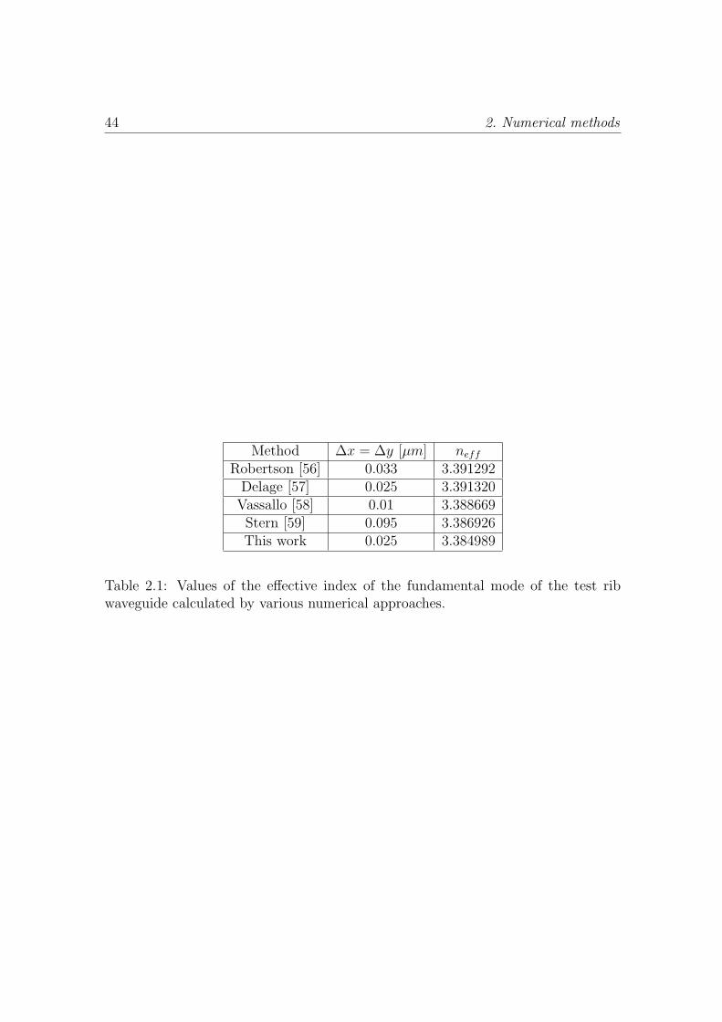
44 2. Numerical methods
Method ∆x = ∆y [µm] neff
Robertson [56] 0.033 3.391292Delage [57] 0.025 3.391320Vassallo [58] 0.01 3.388669Stern [59] 0.095 3.386926This work 0.025 3.384989
Table 2.1: Values of the effective index of the fundamental mode of the test ribwaveguide calculated by various numerical approaches.

3
Device fabrication techniques
3.1 Introduction
In the two previous chapters we have described the theoretical properties ofsegmented waveguides and the tools for their numerical modelling. In this chapter,we will describe the techniques used for their fabrication. In particular we willconcentrate on device realized in Lithium Niobate, which is one of the most popularmaterials used for integrated optical waveguides because of its many properties.It exhibits in fact low propagation losses at the telecommunication wavelengthsof interest, good non linear properties, which allow efficient frequency conversionoperations, and high electro-optical coefficients allowing fabrication of Mach-Zendermodulators and other electronically driven optical circuits.
After recalling the main physical features of Lithium Niobate, we will illustratethe various fabrication steps, the photolitography operations and the photomaskdesign of the devices. The samples obtained with this fabrication procedure presentgood quality shape of the exchanged zone, but require improvements in terms ofsurface roughness and scattering losses for the segmented waveguides.
3.2 Properties of Lithium Niobate
Lithium Niobate, whose chemical formula is LiNbO3, is an anisotropic material.This means that its optical characteristics depend on the propagation of the elec-tromagnetic field direction. Anisotropy is one peculiar characteristic of the crystalsand it is directly related to the particular atom arrangements.
The Lithium Niobate elementary cell belongs to the hexagonal crystallographicsystem. We indicate the crystal axes as X, Y , Z, while a, b, c are the size of thecrystallographic cell and α, β, γ are the angles formed between these three axes, asshown in figure 3.1.
From the optical point of view, Lithium Niobate is an uniaxial crystal. This

46 3. Device fabrication techniques
z
x
y
b
a
c
x
y
g
a b
Figure 3.1: Elementary cell of the Lithium Niobate crystal lattice.
means that the permittivity dielectric tensor ε written with respect to a Cartesianframe presents non zero terms only on the main diagonal and two of them are equal.
εr =
n21(x, y) 0 0
0 n21(x, y) 0
0 0 n23(x, y)
. (3.1)
In this way the secular equation, which describes the plane wave propagation in thelattice, becomes [38]:
[k2 − k2
on21
] · [k2(s21 + s2
2
)n2
1 + k2s23n
23 − k2
on21n
23
]= 0 (3.2)
where k is the wavenumber, while si are the cosine directors of the wavevectorand n1 = n2, n3 are the refractive indices in the x, z directions in the consideredreference system. The solution of equation 3.2 can be obtained solving a system intwo equations:
k2 − k2on
21 = 0
k2s21
n23
+k2s2
2
n23
+k2s2
3
n21
= 0. (3.3)
The first equation does not depend on the considered propagation direction: thecorresponding normal surface is then described by a sphere. This means that forany direction, the propagation constant does not change. This kind of wave iscommonly named ordinary , because everything works like in the isotropic case.
The second equation describes an ellipsoid generated around the rotational zaxis. As a consequence, modifying the propagation direction, the wavenumber kchanges accordingly. This solution is known as the extraordinary wave.
The extraordinary and ordinary refractive indices of the Lithium Niobate mas-sive crystals are well approximated, in their wavelength (chromatic dispersion) and

3.3 Waveguide fabrication 47
temperature dependencies, by the Sellmeier relations 3.4 [60]:
n2o = 4.9048 +
0.11775 + 2.2314 · 10−8(T − 24.5)(T + 24.5 + 546)
λ2 − [0.21802− 2.9671 · 10−8(T − 24.5)(T + 24.5 + 546)]2+
+ 2.1429 · 10−8(T − 24.5)(T + 24.5 + 546)− 0.027153 · λ2
n2e = 4.5820 +
0.09921 + 5.2716 · 10−8(T − 24.5)(T + 24.5 + 546)
λ2 − [0.21090− 4.9143 · 10−8(T − 24.5)(T + 24.5 + 546)]2+
+ 2.2971 · 10−7(T − 24.5)(T + 24.5 + 546)− 0.021940 · λ2 (3.4)
where the wavelength λ is expressed in µm and the temperature T in C. In figure3.2 the extraordinary and ordinary indices are plotted as a function of the wavelengthfor T = 25C in the interval of interest. Lithium Niobate is a non centrosymmetric
0.2 0.4 0.6 0.8 1 1.2 1.4 1.62
2.2
2.4
2.6
2.8
λ [µ m]
Ref
ract
ive
inde
x
Ordinary indexExtraordinary index
Figure 3.2: Extraordinary and ordinary refractive index of the Lithium Niobatecrystal as a function of the wavelength for T = 25C.
crystal and then can exhibit also second order non linear effects. We will not usethis properties and for this reason we refer to specialized books [9] for a completedescription of non linearity effects.
3.3 Waveguide fabrication
In order to realize optical waveguides in a Lithium Niobate substrate, manytechniques have been proposed in the past: out-diffusion [61], titanium indiffusion[62], ion implantation [63], proton exchange [64] and its different implementations(simple Proton Exchange [64], Annealed Proton Exchange, APE [65], Soft Proton
48 3. Device fabrication techniques
Exchange, SPE [66]). Among the PE techniques, we have chosen the SPE processas it does not perturb the crystalline structure of LiNbO3 while other ones do [67,68]. In particular, the ferroelectric domain inversion of Periodically Poled LithiumNiobate (PPLN) devices remains intact after SPE [69].
3.3.1 Soft Proton Exchange
The Soft Proton Exchange process (SPE) in Lithium Niobate substrate is aninteresting and important technique for the fabrication of integrated optical devices.The most important advantage of this technique is the easier way with which thedevices can be realized. The technique is based on the diffusion of hydrogen ions(H+) that penetrate the Lithium Niobate wafer going to tie with oxygen creating athin layer that represents the transmission channel. At the same time, lithium ions(Li+) escape from the substrate in the opposite direction leaving the space for thehydrogen ions. The diffusion process can be written using the following equation:
LiNbO3 + xH+ → Li1−xHxNbO3 + Li+ (3.5)
where x represents the normalized proton concentration.The proton source used with Lithium Niobate is the Benzoic acid (C6H5COOH)with a fraction of Lithium Benzoate (LB). In order to obtain a waveguide, it isnecessary to dispose of a Lithium Niobate substrate cut along one of the threepossible plans, we indicate with X-cut, Y -cut and Z-cut (in our case, crystals wereZ-cut LiNbO3 substrates with diffusion plane orthogonal to the Z axis). The mostimportant parameters for this process are the percentage of LB in the mixture, theTspe (time interval in which the substrate remains in contact with the acid) andthe temperature at which the process happens. Varying %LB between 0 and 5, thenature of the exchanged layer is strongly modified. It is possible to identify threedifferent regimes, as shown in figure 3.3, corresponding to three different ranges of%LB: Proton Exchange (PE), Multiphase Proton Exchange (MPE) and Soft ProtonExchange (SPE). In the left part of figure 3.3 a low value of %LB is considered(0 < %LB < 1%): in this regime the index profile is step with maximum value∆ne between 0.08 and 0.12 at λ = 632.8nm. If %LB is greater than 2.8% theSPE regime is obtained and the shape of the extraordinary index is graded with amaximum ∆ne = 0.03 at λ = 632.8nm. The region named MPE is a combinationof the other two regimes and shows an index shape intermediate between the stepand the graded index.
The PE waveguide allows to obtain strong field confinement improving in thisway the non linear and electro-optic effect efficiency, which depends on the localintensity. Unfortunately, these advantages are canceled by the reduction of the nonlinear and electro-optic coefficients. Contrary to what happens for SPE waveguides,even if the mode is weakly confined, the optical quality provides low propagationlosses and preserves the non linear and electro-optic properties of the substrate. The
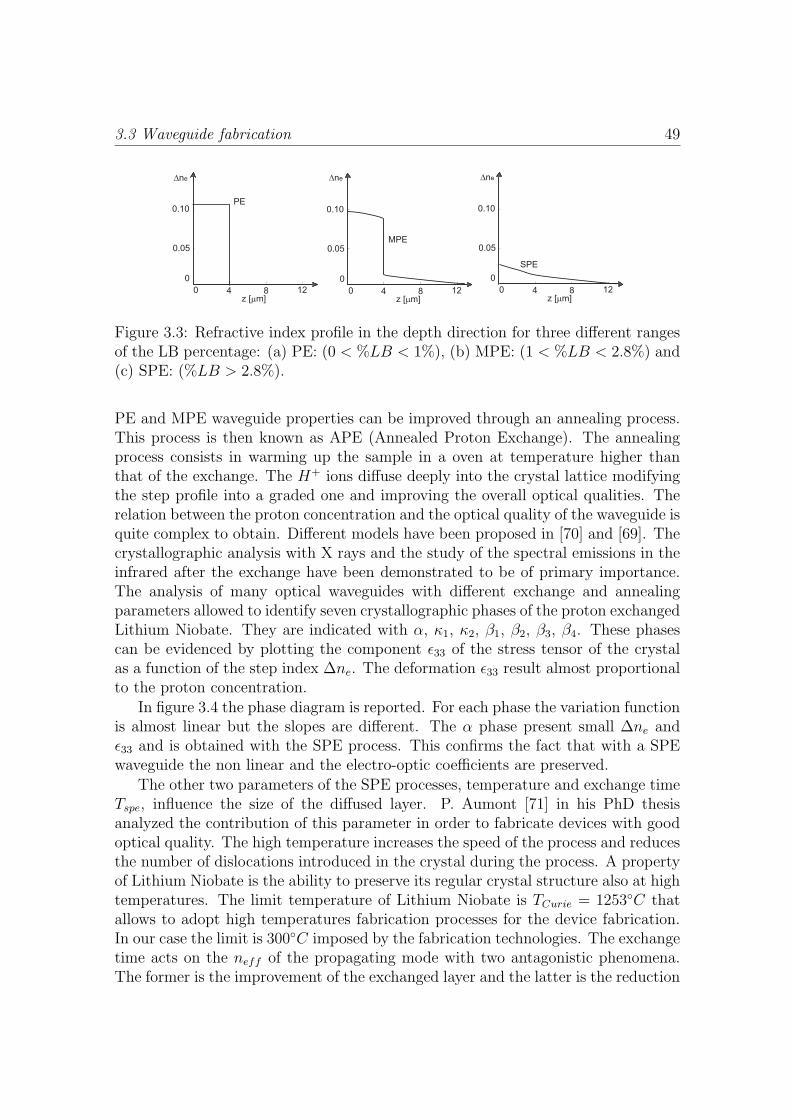
3.3 Waveguide fabrication 49
4 8 12
0.05
0.10
Dne
z [mm]4 8 12
0.05
0.10
z [mm]
0
0 4 8 12
0.05
0.10
z [mm]
0
0
0
0
PE
SPE
MPE
Dne Dne
Figure 3.3: Refractive index profile in the depth direction for three different rangesof the LB percentage: (a) PE: (0 < %LB < 1%), (b) MPE: (1 < %LB < 2.8%) and(c) SPE: (%LB > 2.8%).
PE and MPE waveguide properties can be improved through an annealing process.This process is then known as APE (Annealed Proton Exchange). The annealingprocess consists in warming up the sample in a oven at temperature higher thanthat of the exchange. The H+ ions diffuse deeply into the crystal lattice modifyingthe step profile into a graded one and improving the overall optical qualities. Therelation between the proton concentration and the optical quality of the waveguide isquite complex to obtain. Different models have been proposed in [70] and [69]. Thecrystallographic analysis with X rays and the study of the spectral emissions in theinfrared after the exchange have been demonstrated to be of primary importance.The analysis of many optical waveguides with different exchange and annealingparameters allowed to identify seven crystallographic phases of the proton exchangedLithium Niobate. They are indicated with α, κ1, κ2, β1, β2, β3, β4. These phasescan be evidenced by plotting the component ε33 of the stress tensor of the crystalas a function of the step index ∆ne. The deformation ε33 result almost proportionalto the proton concentration.
In figure 3.4 the phase diagram is reported. For each phase the variation functionis almost linear but the slopes are different. The α phase present small ∆ne andε33 and is obtained with the SPE process. This confirms the fact that with a SPEwaveguide the non linear and the electro-optic coefficients are preserved.
The other two parameters of the SPE processes, temperature and exchange timeTspe, influence the size of the diffused layer. P. Aumont [71] in his PhD thesisanalyzed the contribution of this parameter in order to fabricate devices with goodoptical quality. The high temperature increases the speed of the process and reducesthe number of dislocations introduced in the crystal during the process. A propertyof Lithium Niobate is the ability to preserve its regular crystal structure also at hightemperatures. The limit temperature of Lithium Niobate is TCurie = 1253C thatallows to adopt high temperatures fabrication processes for the device fabrication.In our case the limit is 300C imposed by the fabrication technologies. The exchangetime acts on the neff of the propagating mode with two antagonistic phenomena.The former is the improvement of the exchanged layer and the latter is the reduction

50 3. Device fabrication techniques
e
k
k
a
b b
b
b
.10 2 3 4 5 6
0.05
0.1
0.15
1
2 12
3
4
eDn
3310
-3
Figure 3.4: Phase diagram for the proton exchanged Lithium Niobate crystal.
of the ∆ne. The higher neff can be obtained with exchange time of three days (72hours).
In order to fabricate the SPE waveguide, we have used the immersion techniquethat consists in using an ampoule with a throttling in the center. The proton sourceis placed in the lower part of the ampoule while the masked Lithium Niobate crystalin the upper part (throttling prevents the contact between the two components).The ampoule is then connected to a vacuum pump that can create the desireddepressurization. After that the ampoule is closed with a flame. The ampoule isthen placed into an iron pipe which protect the environment in the case of explosionand provide an important thermic inertia. The pipe is then placed in the oven atthe temperature of 300C. The fusion temperature of the Benzoic acid is 160Cwhile for the Lithium Benzoate LB it is much more higher than 300C. Fortunately,LB is soluble in the liquid Benzoic acid and in this way we obtain a liquid mixture.When the temperature is stabilized we can just turn the pipe in order to put thesample and the proton source in contact. From this moment the exchange begins.After 72 hours we turn off the oven and the pipe is turned once again. When it iscold the sample can be taken out.
3.4 Photolithography
In order to fabricate segmented waveguide devices it is necessary to control thediffusion process. This can be done by masking the surface of the Lithium Niobateusing photolithography. This word, which in Greek means “writing on a stone with

3.4 Photolithography 51
light”, is used to describe the process by which patterns on a LiNbO3 substrate canbe defined using light. The absence of dust is an essential condition to obtain goodresults from this technique and for this reason all the step we are going to illustrateare made in the clean room of the Centre de Recherche sur l’Hetero-Epitaxie etses Applicationsas (CRHEA) of Valbonne-Sophia-Antipolis with the collaborationof Sorin Tascu (post doctorate at the LPMC of the university of Nice Sophia An-tipolis). A schematization of the different steps is shown in figure 3.5. Before the
LiNbO3
U.V.
LiNbO3
Photoresist
Chrome
Quartz
LiNbO3
SiO2
LiNbO3
200nm
LiNbO3
200nm
LiNbO3
Photoresist
700nm
Photoresist
700nm
(a) (b)
(c) (d)
(e) (f)
SiO2
Photoresist
Figure 3.5: Schematization of the photolitography process.
photoresist is applied to the substrate, the surface is cleaned to remove any traces ofcontamination from the surface of the wafer such as dust, organic, ionic and metal-

52 3. Device fabrication techniques
lic compounds. The cleaned wafer is subject to priming, to aid the adhesion of thephotoresist to the surface of the substrate material.
A 700 nm thick layer of photoresist is applied to the surface using a spin-coatingmachine (figure 3.6). This device holds the wafer of semiconductor, using a vacuumpump, and spins the photoresist at high-speed for a period of 15-30 seconds. A smallquantity of photoresist is put on the center of the spinning wafer. The rotation causesthe photoresist to be spread across the surface of the wafer with excess being thrownoff. Preparation of the photoresist is concluded by a bake, where the wafer is heatedin a oven to partially solidify the photoresist.
Figure 3.6: Picture of the spin coating machine used for the photoresist depositionon the wafer.
The photomask with the shape of our optical devices is created by a photographicprocess and developed onto a quartz substrate for its mechanical and optical prop-erties.
Alignment between photomask and wafer is critical and must be achieved inx and y directions as well as rotationally. Photolithography machines use patternrecognition to achieve a so presise alignment (figure 3.7).
During the exposure process, the photoresist undergoes a chemical reaction. De-pending on the chemical composition of photoresist, it can react in two ways whenthe light strikes the surface. The action of light on a positive photoresist causes it tobecome polymerized where it has been exposed to the light. A negative photoresisthas the reverse property. Exposure to UV-light cause the photoresist to decom-pose. Preliminary experiments have shown that using a negative photoresist all thedimensions of our structures are reduced by about 1µm respect to the photomaskreference. This is the reason for which we have fabricated our device using a positivephotoresist.
After the develop process the sample is ready for the deposition of 200nm thickSiO2 layer over all the surface of the wafer. The final SiO2 mask is obtained witha lift-off process which removes the resit through chemical reaction.

3.4 Photolithography 53
Figure 3.7: Picture of the photolithography machines used for the UV exposition.
3.4.1 Photomask design
To draw the photomask we have used Wavemaker [72]. This commercial CADprovides a graphical interface to realize the schematic of optical components, allow-ing to save the final draft in the standard format (.gds) used by the facilities whichproduce photomasks. In our case the photomask has been fabricated by Photronics(UK) [73].
Segmented waveguides and tapers are structures constituted by hundreds of seg-ments, each one with different size depending on the device parameters (taper length,width, DC etc.). It is, therefore, impossible to draw this kind of photomask for athree inches wafer adopting the standard “cut and paste” procedure or similar com-mands available in the CAD. We have then used the scripting language availablein Wavemaker in order to automatize the photomask preparation. In this way, allthe “draw” command can be given through an external file instead of the standardgraphic interface. We have developed a Fortran program that acquires the descrip-tions of all the devices we want to put in the photomask from an input file (.txt).This input file follows rules fixed by us, without entering in the details of the singlesegments. After the execution of our program we obtain a command file (.cmd)compatible with the scripting language of Wavemaker and a control file (.log) whichsummarizes all the parameters of the plotted devices. A flow chart of this processis shown in figure 3.8
This tool has been very useful during the photomask preparation allowing toobtain very fastly the desired results correctly.
A very important parameter to take into account during the photomask design isthe distance to maintain between two neighbouring devices, fabricated on the samesubstrate, in order to avoid unwanted interferences but at the same time preserving

54 3. Device fabrication techniques
Figure 3.8: Schematization of the photomask preparation using the numerical toolsimplemented to interface with the CAD Wavemaker.
space. The problem can be resolved by making a study on the coupling interactionoccurring between integrated optical waveguides with the complication that in ourcase the coupled waveguides are segmented.
The coupling phenomena is strongly related to the evanescent tails of the twoelectromagnetic modes that propagate in the waveguides and must be accuratelyevaluated. For this reason, we have adopted the 3D BPM for the numerical analysisof this problem. In this case, we can not apply the equivalent waveguide theoremand adopt the mode solver to obtain a precise evaluation of the coupling. The reasonis that during the propagation the mode is modulated by the periodic structure [74].This modulation is not present when modelling the segmented waveguide with anequivalent continuous waveguide: as a consequence, the coupling effect would beperturbed.
The analysis we have made consists in evaluating the coupling effect simplychanging the distance between two parallel segmented waveguides. The worst casehappens when the field is less confined and the overlap between the two modes isthen more important. As a consequence, for the segmented waveguide parameters,we have considered the less confined structure with period P = 25 µm, duty cycleDC = 0.4 and waveguide width W = 5µm and working wavelength equal to 1.55 µm.Using the BPM it is possible to evaluate the power evolution in the two waveguidein the propagation direction z 1 and then obtain the coupling length Lc. Figure 3.9shows the power distribution for two segmented waveguides placed at the center tocenter distance d = 10 µm.
For the same structure in figure 3.10 the field distributions in horizontal andvertical sections are shown. Note that the energy can completely be transfered fromone guide to the other one as the two segmented waveguide are identical.
Repeating the simulation for different distances d between the two segmented
1Note that in the following, z will refer to the propagation direction, which is different to thecrystal axis Z of the Lithium Niobate substrate
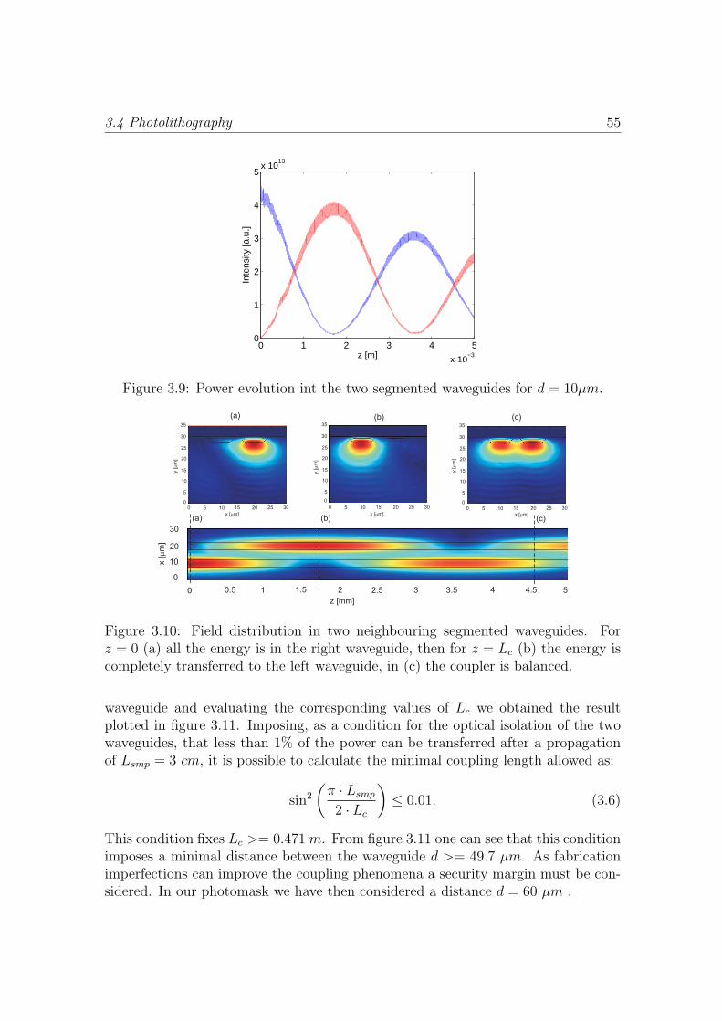
3.4 Photolithography 55
0 1 2 3 4 5
x 10−3
0
1
2
3
4
5x 10
13
z [m]
Inte
nsity
[a.u
.]
Figure 3.9: Power evolution int the two segmented waveguides for d = 10µm.
0 0.5 1 1.5 2 2.5 3 3.5 4 4.5 5
0
10
20
30
z [mm]
x [m
m]
5 10 15 20 25 300
5
10
15
20
25
30
35
05 10 15 20 25 300
5
10
15
20
25
30
35
0
5 10 15 20 25 300
5
10
15
20
25
30
35
0
(a) (b) (c)
y [m
m]
y [m
m]
y [m
m]
x [mm] x [mm] x [mm](a) (b) (c)
Figure 3.10: Field distribution in two neighbouring segmented waveguides. Forz = 0 (a) all the energy is in the right waveguide, then for z = Lc (b) the energy iscompletely transferred to the left waveguide, in (c) the coupler is balanced.
waveguide and evaluating the corresponding values of Lc we obtained the resultplotted in figure 3.11. Imposing, as a condition for the optical isolation of the twowaveguides, that less than 1% of the power can be transferred after a propagationof Lsmp = 3 cm, it is possible to calculate the minimal coupling length allowed as:
sin2
(π · Lsmp
2 · Lc
)≤ 0.01. (3.6)
This condition fixes Lc >= 0.471 m. From figure 3.11 one can see that this conditionimposes a minimal distance between the waveguide d >= 49.7 µm. As fabricationimperfections can improve the coupling phenomena a security margin must be con-sidered. In our photomask we have then considered a distance d = 60 µm .
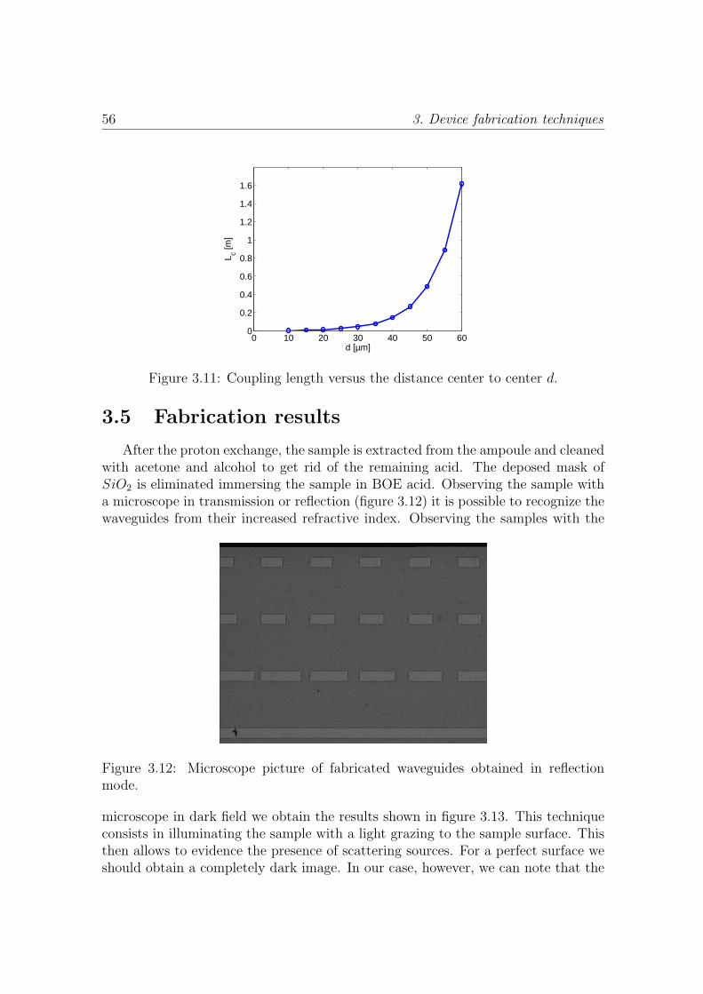
56 3. Device fabrication techniques
0 10 20 30 40 50 600
0.2
0.4
0.6
0.8
1
1.2
1.4
1.6
d [µm]
L c [m]
Figure 3.11: Coupling length versus the distance center to center d.
3.5 Fabrication results
After the proton exchange, the sample is extracted from the ampoule and cleanedwith acetone and alcohol to get rid of the remaining acid. The deposed mask ofSiO2 is eliminated immersing the sample in BOE acid. Observing the sample witha microscope in transmission or reflection (figure 3.12) it is possible to recognize thewaveguides from their increased refractive index. Observing the samples with the
Figure 3.12: Microscope picture of fabricated waveguides obtained in reflectionmode.
microscope in dark field we obtain the results shown in figure 3.13. This techniqueconsists in illuminating the sample with a light grazing to the sample surface. Thisthen allows to evidence the presence of scattering sources. For a perfect surface weshould obtain a completely dark image. In our case, however, we can note that the

3.5 Fabrication results 57
Figure 3.13: Dark field image of two fabricated segmented waveguide.
edges of our waveguides are visible. This result shows the presence of bulges or sinksin the contour of the exchanged zones. This problem has required a more advancedanalysis. Using a AFM (Atomic Force Microscope) Sorin Tascu (post doctorate atthe LPMC of the university of Nice Sophia Antipolis) confirmed the presence ofsinks of about 50 nm of depth. This phenomenon clearly increases the propagationlosses of continuous and segmented waveguides. We report in the following tablethe propagation losses of our fabricated waveguides. The measurement techniqueadopted for this characterization will be described with more details in the nextchapter.
P = 15µm P = 25µmDC W = 5µm W = 7µm W = 5µm W = 7µm0.5 2 dB/cm 2.34 dB/cm 4 dB/cm 2.99 dB/cm0.6 1.71 dB/cm 2.02 dB/cm 2.92 dB/cm 2.02 dB/cm0.7 1.74 dB/cm 2.16 dB/cm 2.40 dB/cm 2.04 dB/cm1 1.13 dB/cm 1.34 dB/cm 1.13 dB/cm 1.34 dB/cm
The possible causes to explain this roughness phenomena and the consequentlyelevated propagation losses respect to smaller expected values are:
• the crystal structure of Lithium Niobate is perturbed during the photoresistdeposition;
• the crystal structure of Lithium Niobate is perturbed during the SiO2 depo-sition;
• the acid BOE attacks the Lithium Niobate surface during the elimination ofthe deposed SiO2 mask;
• the Lithium Niobate crystal structure is fragilized during the SPE process.

58 3. Device fabrication techniques
The first three possibilities have been rapidly excluded repeating the procedure ofphotoresist and SiO2 deposition on the Litium Niobate substrate. We have thenremoved the two depositions with acetone and BOE to obtain a perfect surfacewithout any kind of imperfections. The only remaining possibility is then that ofthe fragilization induced by the SPE. During the exchange the sample is subjectto acid contact at hight temperatures: this stress is probably too strong for thecrystal structure. To confirm this hypothesis PE and APE waveguides have beenfabricated as they require reduced exchange time. For both of them no defectsappear on the surface. It is then necessary that future work will study in moredetails this phenomenon to allow fabrication of better quality SPE waveguides withlow propagation losses.
3.5.1 M-lines characterization
One side of the sample during the SPE being unmasked is completely exchangedand the resulting increase of the refractive index forms a slab waveguide. Thepresence of this waveguide can be used to determine the optical properties of thedevice fabricated on the other side of the sample. Using the m-lines techniques [75],it is also possible, in fact, to measure the effective index of the propagating modesof the slab. Then, using the Inverse-WKB (IWKB) technique [76, 77] it is possibleto reconstruct the refractive index profile in the vertical direction for the exchangedzones. With the m-lines technique it is also possible evaluate qualitatively the opticalproperties of the sample under test.
A schematic of the m-lines experimental setup is shown in figure 3.14.
Rutile prisms
He-Ne: Laser
Mirror
Sample
Screen
Normal
Autocollimated
monocular
q
Figure 3.14: Experimental setup for the m-lines characterization.
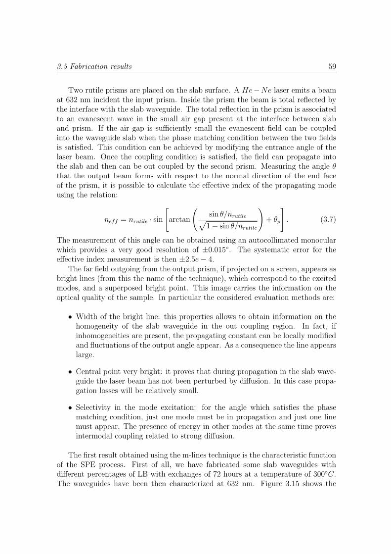
3.5 Fabrication results 59
Two rutile prisms are placed on the slab surface. A He−Ne laser emits a beamat 632 nm incident the input prism. Inside the prism the beam is total reflected bythe interface with the slab waveguide. The total reflection in the prism is associatedto an evanescent wave in the small air gap present at the interface between slaband prism. If the air gap is sufficiently small the evanescent field can be coupledinto the waveguide slab when the phase matching condition between the two fieldsis satisfied. This condition can be achieved by modifying the entrance angle of thelaser beam. Once the coupling condition is satisfied, the field can propagate intothe slab and then can be out coupled by the second prism. Measuring the angle θthat the output beam forms with respect to the normal direction of the end faceof the prism, it is possible to calculate the effective index of the propagating modeusing the relation:
neff = nrutile · sin[arctan
(sin θ/nrutile√
1− sin θ/nrutile
)+ θp
]. (3.7)
The measurement of this angle can be obtained using an autocollimated monocularwhich provides a very good resolution of ±0.015. The systematic error for theeffective index measurement is then ±2.5e− 4.
The far field outgoing from the output prism, if projected on a screen, appears asbright lines (from this the name of the technique), which correspond to the excitedmodes, and a superposed bright point. This image carries the information on theoptical quality of the sample. In particular the considered evaluation methods are:
• Width of the bright line: this properties allows to obtain information on thehomogeneity of the slab waveguide in the out coupling region. In fact, ifinhomogeneities are present, the propagating constant can be locally modifiedand fluctuations of the output angle appear. As a consequence the line appearslarge.
• Central point very bright: it proves that during propagation in the slab wave-guide the laser beam has not been perturbed by diffusion. In this case propa-gation losses will be relatively small.
• Selectivity in the mode excitation: for the angle which satisfies the phasematching condition, just one mode must be in propagation and just one linemust appear. The presence of energy in other modes at the same time provesintermodal coupling related to strong diffusion.
The first result obtained using the m-lines technique is the characteristic functionof the SPE process. First of all, we have fabricated some slab waveguides withdifferent percentages of LB with exchanges of 72 hours at a temperature of 300C.The waveguides have been then characterized at 632 nm. Figure 3.15 shows the
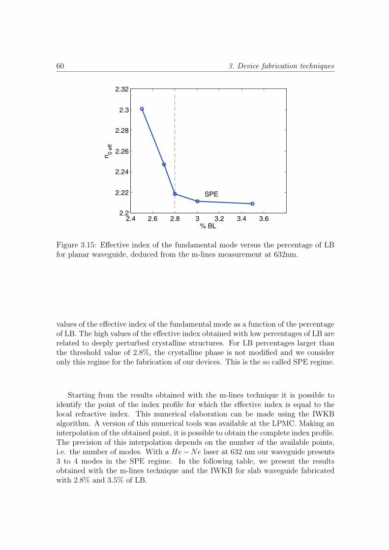
60 3. Device fabrication techniques
2.4 2.6 2.8 3 3.2 3.4 3.62.2
2.22
2.24
2.26
2.28
2.3
2.32
% BL
n0
eff
SPE
Figure 3.15: Effective index of the fundamental mode versus the percentage of LBfor planar waveguide, deduced from the m-lines measurement at 632nm.
values of the effective index of the fundamental mode as a function of the percentageof LB. The high values of the effective index obtained with low percentages of LB arerelated to deeply perturbed crystalline structures. For LB percentages larger thanthe threshold value of 2.8%, the crystalline phase is not modified and we consideronly this regime for the fabrication of our devices. This is the so called SPE regime.
Starting from the results obtained with the m-lines technique it is possible toidentify the point of the index profile for which the effective index is equal to thelocal refractive index. This numerical elaboration can be made using the IWKBalgorithm. A version of this numerical tools was available at the LPMC. Making aninterpolation of the obtained point, it is possible to obtain the complete index profile.The precision of this interpolation depends on the number of the available points,i.e. the number of modes. With a He−Ne laser at 632 nm our waveguide presents3 to 4 modes in the SPE regime. In the following table, we present the resultsobtained with the m-lines technique and the IWKB for slab waveguide fabricatedwith 2.8% and 3.5% of LB.

3.6 Polishing 61
M-lines thecnique IWKBLB percentage Angle [deg] effective index @ 632.8µm Deep [µm]
10.926 2.21848 1.482.8 % 9.841 2.20874 2.651
9.383 2.20459 4.8829.227 2.20318 8.939.888 2.20916 2.182
3.5 % 9.374 2.20451 3.8229.181 2.20276 7.562
Using interpolation techniques we have reconstructed the two profiles shown in figure3.16.
0 2 4 6 8
2.205
2.21
2.215
2.22
2.225
2.23
Deep [mm]
n
3.5% LB
fitted profile 3.5% LB
2.8% LB
fitted profile 2.8% LB
Figure 3.16: Index profile reconstructed using the IWKB algorithm after the m-linesmeasurement on SPE waveguide with different LB percentage: LB%=3.5 (red line),LB%=2.8 (blue dashed line).
3.6 Polishing
In order to couple energy into an optical waveguide different techniques havebeen developed. One of these solutions has been already presented describing them-lines experimental setup. It consists in using two prisms as shown in figure 3.17.For channel waveguides this solution is very difficult to use as alignment is notsimple. Another solution proposed in the past [78] uses diffracting gratings at the
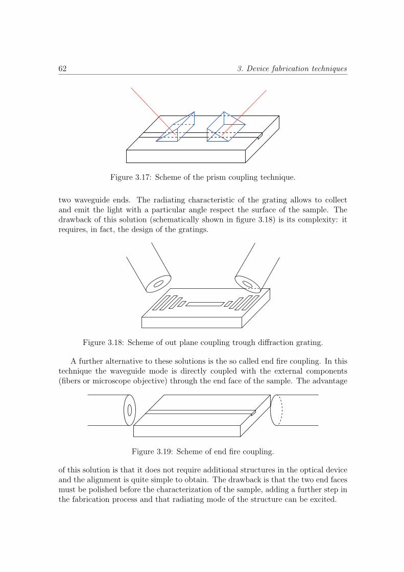
62 3. Device fabrication techniques
Figure 3.17: Scheme of the prism coupling technique.
two waveguide ends. The radiating characteristic of the grating allows to collectand emit the light with a particular angle respect the surface of the sample. Thedrawback of this solution (schematically shown in figure 3.18) is its complexity: itrequires, in fact, the design of the gratings.
Figure 3.18: Scheme of out plane coupling trough diffraction grating.
A further alternative to these solutions is the so called end fire coupling. In thistechnique the waveguide mode is directly coupled with the external components(fibers or microscope objective) through the end face of the sample. The advantage
Figure 3.19: Scheme of end fire coupling.
of this solution is that it does not require additional structures in the optical deviceand the alignment is quite simple to obtain. The drawback is that the two end facesmust be polished before the characterization of the sample, adding a further step inthe fabrication process and that radiating mode of the structure can be excited.

3.6 Polishing 63
The polishing technique we have used consists to fix vertically the sample betweentwo piece of glass inside a metallic support. The presence of the two pieces of glassprovides a better stability to the sample and improves the edge quality. The metallicsupport is then mounted into a Sample Mounting Fixture (SMF) to apply uniformpressure to the sample during polishing. The SMF is then placed on a rotating plateand its position is controlled by a mechanical arm. Suitable abrasive products mustbe put on the plate to improve grinding and polishing of the sample end face. In ourcase, we have adopted dust of alumina mixed in water. The procedure consists tostart the polishing with big grains of alumina for an approximative result since usingsmall grain of alumina and a chemical attack for the final step. The table summarizesthe polishing time corresponding to the size of the alumina grains adopted:
Step Alumina size [µm] Time [min]1 20 152 9 303 5 30
The polish procedure with alumina is only mechanical and can be realized with amachine shown in the left part of figure 3.20. The last step requires a more accurate
.
Figure 3.20: Pictures of the two polish machine used for the alumina (left) or chem-ical (right) step.
surface polishing and can be obtained using a particular plate (see right part offigure 3.20), adding a liquid product that attacks chemically the end face of thesample. Care is required to avoid the presence of big grains that can produce deepscratches which would prevent good quality samples.

64 3. Device fabrication techniques
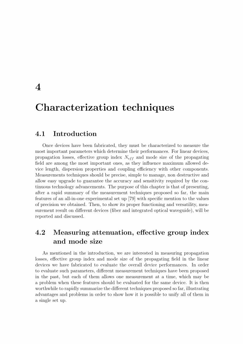
4
Characterization techniques
4.1 Introduction
Once devices have been fabricated, they must be characterized to measure themost important parameters which determine their performances. For linear devices,propagation losses, effective group index Neff and mode size of the propagatingfield are among the most important ones, as they influence maximum allowed de-vice length, dispersion properties and coupling efficiency with other components.Measurements techniques should be precise, simple to manage, non destructive andallow easy upgrade to guarantee the accuracy and sensitivity required by the con-tinuous technology advancements. The purpose of this chapter is that of presenting,after a rapid summary of the measurement techniques proposed so far, the mainfeatures of an all-in-one experimental set up [79] with specific mention to the valuesof precision we obtained. Then, to show its proper functioning and versatility, mea-surement result on different devices (fiber and integrated optical waveguide), will bereported and discussed.
4.2 Measuring attenuation, effective group index
and mode size
As mentioned in the introduction, we are interested in measuring propagationlosses, effective group index and mode size of the propagating field in the lineardevices we have fabricated to evaluate the overall device performances. In orderto evaluate such parameters, different measurement techniques have been proposedin the past, but each of them allows one measurement at a time, which may bea problem when these features should be evaluated for the same device. It is thenworthwhile to rapidly summarize the different techniques proposed so far, illustratingadvantages and problems in order to show how it is possible to unify all of them ina single set up.

66 4. Characterization techniques
Propagation losses can be evaluated in a conceptually very simple way using theso called insertion losses technique [80]. The Device Under Test (DUT) is insertedbetween two identical fibers. The transmitted power is measured and attenuationis obtained comparing this value to that resulting from direct connection of the twofibers. Such technique is conceptually very simple, but requires the knowledge ofthe overlap integral between the fiber mode and that of the DUT input and outputsections. Moreover, systematic errors can come from alignment problems and pos-sible formation of parasitic air cavities between the fiber and the sample interfacethat can perturb the transmission power measurement. Some of these problemsare eliminated by the so called back coupling method [81]. This technique assumesthat all guided field outgoing the DUT can be reflected and coupled back into itby a proper optical system. If such an operation is lossless, only Fresnel losses oc-cur. Overall transmission losses can then be determined comparing the intensitiesof the launched beam and that of the back reflected light after double passing theDUT. The precision of this technique critically depends on the quality of both theinput beam splitter and the output reflecting optical system. A further method isbased on the assumption that the power laterally scattered by the DUT is linearlyproportional to the guided one. Measuring its evolution during propagation (witha camera or any other sensor) allows an indirect evaluation of DUT attenuation[82, 74]. This measurement technique is simple, but has problems both in highloss devices because of the presence of scattering centers and in low loss devices,where very long samples are required for loss evaluation. A fourth method used forpropagation losses measurement is the so called Fabry-Perot resonance technique[83]. The sample acts as a cavity whose quality factor and finesse depend on thepropagation losses. A tunable laser source with narrow linewidth allows spectralcharacterization of the cavity parameters providing also its propagation losses, af-ter some data processing. This technique requires careful sample preparation andalignment procedures to avoid again parasitic air cavities outside the DUT. It workswell for low losses measurements (under 3-4 dB/cm) and its precision depends onthe sample length.
The second parameter to be measured is the effective group index Neff of apropagating mode [84], which establishes the dispersive behavior of an optical wave-guide. Fiber suppliers are interested in such a parameter and many measurementsetups have been then proposed so far: for example, the so called time of flightmeasurement [85, 86] or other interferential techniques [87, 88]. But they are notfully general as they cannot be used for integrated optical devices. Today, the inter-est for measuring such a parameter is still strong as, for example, photonic crystalwaveguides [89, 90, 91, 92] can be used for slow light guidance [93, 94] and the Neff
measurement is then fundamental for their characterization. A method to evaluateNeff in integrated optical waveguides is based on a spectral measurement of thefield mode size [95, 96]. The precision of this method depends on the accuracy ofthe mode size measurement and on how good is the approximation of the relation

4.3 Experimental setup 67
between the waveguide dispersion and the mode size. A different approach is basedon the characterization of the Fabry-Perot cavity formed by the sample, as previ-ously discussed talking about propagation loss measurements. In this case, in fact,the distance between the resonance peaks depends on the value of Neff [97].
Finally, the field distribution of the modes guided by the DUT is most of thetime obtained by measuring the near field by a camera [98]. Problems of this setupcome from nonlinearity and inhomogeneity of the sensor, aberrations of the lens usedto magnify the near field image and difficult calibration of the whole measurementsetup. To overcome these problems, the near field is evaluated scanning the DUTend-face with a 1-µm-diameter pinhole in a 2.5-µm-thick steel sheet mounted ona single-mode fiber connected to the detector [99]. The price to pay is a muchlonger measurement time, requiring setup and source thermal stabilization. Far fieldmeasurements and subsequent Hankel transform to reconstruct the near field havealso been proposed [100]. They eliminate the risks connected to close and movingparts, which may damage optical surfaces, but are not precise, as the evanescentpart of the plane wave spectrum composing the near field is not present in the farfield and so the field reconstruction is not precise.
As one can see, measurement procedures to evaluate all these parameters arecumbersome, time consuming and are affected by systematic errors depending oneach particular setup. So we have conceived and realized an all-in-one measurementsetup to evaluate propagation losses, effective group index Neff and mode size ofthe propagating field of both optical fibers and integrated optical waveguides. Thissolution, which will be described in the next section, reduces measurement time,saves space and allows optimizing all the setup parameters only once, thus providingmeasurements results affected by the same measurement errors. This also allowssimpler upgrade to higher measurement precision, when needed.
The setup is conceived also to collect all the best features of the previouslyillustrated ones. The loss and effective group index measurement principle is basedon the Fabry-Perot cavity. The mode size measurement is based on the idea proposedin [99], but with improvements in terms of precision of the results and simplicity ofthe experimental setup because only a monomode fiber has been used to performthe scan.
4.3 Experimental setup
The schematic of the measurement setup is shown in figure 4.1. The laser sourceis a tunable external cavity laser emitting between 1.5 µm and 1.6 µm (NetTest Tu-nics Plus) with an automatic power control system and a linewidth as narrow as 150kHz. To allow polarization controlled measurements, the laser output is connectedto a polarization maintaining fiber, monomode at the working wavelengths. Theother fiber end is fixed on a piezoelectric positioning system. Such system allows

68 4. Characterization techniques
controlling the position of the fiber on the x-y plane in a range of 25 µm × 25 µmwith step of 16 nm. With micrometric controls, it is also possible to adjust the hor-izontal (Θh) and vertical incidence angles (Θv) of the fiber with respect to the opticaxis. On the other side of the DUT, a SMF28 fiber is fixed on a similar piezoelectricpositioning system with the same features as the previous one in order to collect theoutput signal. The SMF28 fiber output is connected to an InGaAs detector for theintensity measurement. The piezoelectric stages and the detector are connected to acontrol station that allows the interface with a Personal Computer (PC) through aGPIB port. A Labview R© [101] program controls all the measurements and provides
Optical isolator
PM-Fiber SMF28
Piezo
Controller
GPIB
Computer
Detector
zx
y
Piezo
DUTTunable Laser
Figure 4.1: Schematic of the all-in-one experimental setup to measure propagationlosses, effective group index and mode size of an optical fiber or an integrated opticaldevice (DUT: Device Under Test).
rapid and reproducible data collection. The remote control of the measurementfrom the PC offers many advantages, not only related to increased reproducibilityand precision. For example, there is no need for operators to get close or touch thecomponents. This avoids mechanical changes due to temperature variations in thesetup, which are critical when long measurements must be performed. Figure 4.2shows a screenshot of the program interface. The DUT is surrounded by air andits end-faces form a Fabry-Perot cavity. As said before, once the cavity parametersare known, values of both propagation losses and Neff can be obtained. Moreover,the possibility to scan the output section of the DUT by moving the SMF28 fiberallows also obtaining information on the shape of the field that propagates throughthe sample. In the following subsections, more details on the different measurementtechniques integrated in this setup will be provided.
4.3.1 Loss measurements
The Fabry-Perot based technique to evaluate propagation losses L is based onthe fact that the guided mode of the DUT is partially reflected at the end-faces of

4.3 Experimental setup 69
Figure 4.2: Screenshot of the Labview R© program used to control the experimentalsetup.
the sample. This is due to the difference between the refractive index of air andthe effective index of the propagating mode, neff , defined as the ratio between thepropagation constant β and the wavenumber k0. The waveguide behaves then asa resonant cavity and modes propagating in both directions interfere according totheir relative phases. Resonance conditions depend on wavelength. Their periodicoccurrence can be evidenced by a spectral scanning of the transmission character-istics. Such a transmission spectrum is characterized by the so called contrast C,which is defined as:
C =Imax − Imin
Imax + Imin
(4.1)
being Imax and Imin the maximum and the minimum output intensities respectively.Assuming orthogonally polished end-faces with respect to the waveguide, the prop-agation losses L (evaluated in dB) can be obtained by measuring C and using [83]:
L = 4.34
[ln
1−√1− C2
C− ln (R)
](4.2)
where R is the end-face (Fresnel) reflection coefficient:
R =(neff − 1)2
(neff + 1)2. (4.3)
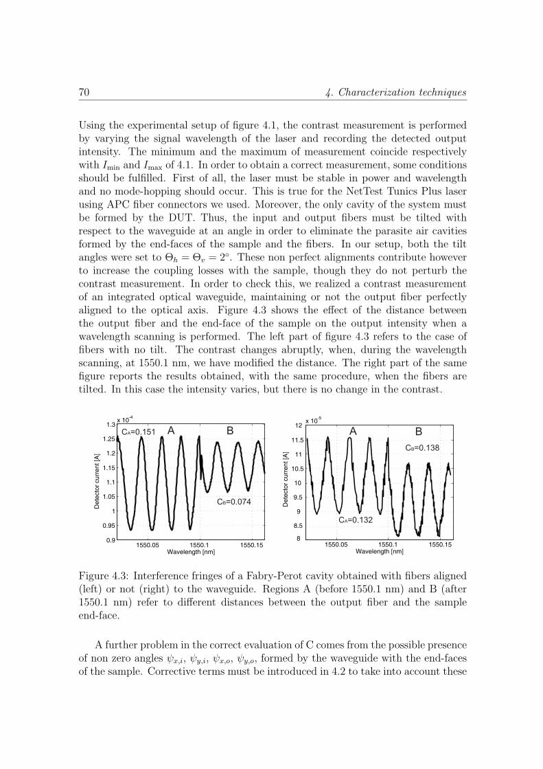
70 4. Characterization techniques
Using the experimental setup of figure 4.1, the contrast measurement is performedby varying the signal wavelength of the laser and recording the detected outputintensity. The minimum and the maximum of measurement coincide respectivelywith Imin and Imax of 4.1. In order to obtain a correct measurement, some conditionsshould be fulfilled. First of all, the laser must be stable in power and wavelengthand no mode-hopping should occur. This is true for the NetTest Tunics Plus laserusing APC fiber connectors we used. Moreover, the only cavity of the system mustbe formed by the DUT. Thus, the input and output fibers must be tilted withrespect to the waveguide at an angle in order to eliminate the parasite air cavitiesformed by the end-faces of the sample and the fibers. In our setup, both the tiltangles were set to Θh = Θv = 2. These non perfect alignments contribute howeverto increase the coupling losses with the sample, though they do not perturb thecontrast measurement. In order to check this, we realized a contrast measurementof an integrated optical waveguide, maintaining or not the output fiber perfectlyaligned to the optical axis. Figure 4.3 shows the effect of the distance betweenthe output fiber and the end-face of the sample on the output intensity when awavelength scanning is performed. The left part of figure 4.3 refers to the case offibers with no tilt. The contrast changes abruptly, when, during the wavelengthscanning, at 1550.1 nm, we have modified the distance. The right part of the samefigure reports the results obtained, with the same procedure, when the fibers aretilted. In this case the intensity varies, but there is no change in the contrast.
1550.05 1550.1 1550.15
9
9.5
10
10.5
11
11.5
12x 10
-5
Wavelength [nm]
Dete
cto
r curr
ent [A
]
A B
8.5
8
CB=0.138
CA=0.132
1550.05 1550.1 1550.150.9
0.95
1
1.05
1.1
1.15
1.2
1.25
1.3x 10
-4
Wavelength [nm]
Dete
cto
r curr
ent [A
]
A B
CB=0.074
CA=0.151
Figure 4.3: Interference fringes of a Fabry-Perot cavity obtained with fibers aligned(left) or not (right) to the waveguide. Regions A (before 1550.1 nm) and B (after1550.1 nm) refer to different distances between the output fiber and the sampleend-face.
A further problem in the correct evaluation of C comes from the possible presenceof non zero angles ψx,i, ψy,i, ψx,o, ψy,o, formed by the waveguide with the end-facesof the sample. Corrective terms must be introduced in 4.2 to take into account these

4.3 Experimental setup 71
angles [80]:
R =(neff − 1)2
(neff + 1)2·√
Lx,iLx,o
√Ly,iLy,o (4.4)
In this equation
Lx,i = e(−β2i w2
y,iψ2x,i) Lx,o = e(−β2
ow2y,oψ2
x,o)
Ly,i = e(−β2i w2
x,iψ2y,i) Ly,o = e(−β2
ow2x,oψ2
y,o) (4.5)
being βi and βo the input and output wavevectors respectively, while wx,i, wx,o, wy,i,wy,o are the mode size in the x and y direction at the input and output end face of thesample. As these angles can be easily evaluated with a precisions of 0.1, the effect ofthe angle measurements uncertainty on the determination of the propagation lossescan be practically eliminated. In conclusion, the main contribution to the overallmeasurement error comes from the noise introduced by the acquisition system whenevaluating the contrast C. Note however that, contrary to what happens usingmost of the classical methods of measuring waveguide losses, the error decreasesfor decreasing attenuation as the contrast increases accordingly. For devices withvery low propagation losses the limit of this technique then comes basically fromthe precision determining the neff of the propagating mode and the noise of theexperimental setup for the contrast evaluation. This noise depends on the adoptedsetup and its evaluation can be obtained by repeating the same measurement andobserving the dispersion of the results. With our setup, exploiting the featuresof the remote control, we obtain a fluctuation of the contrast value in reapitedmeasurements of just 0.5%.
4.3.2 Group index and dispersion measurements
With the same configuration of the experimental setup used for loss measurementwe can obtain also the effective group index Neff of the propagation mode in awaveguide, with Neff defined as:
c
vg
= Neff (λ0) = neff (λ0)− λ0∂neff (λ0)
∂λ0
(4.6)
where c is the speed of light in vacuum, vg is the group velocity and λ0 is thefree space wavelength. As we can see, Neff takes into account both propagationand dispersion characteristics. The value of Neff comes from the knowledge ofthe free spectral range ∆λ of the transmission spectrum [84]. To determine therelationship between Neff and the measurement results, one can start from theresonance conditions corresponding to maximum power transmission:
2 · 2π
λ0
· neff (λ0) · L = 2mπ (4.7)

72 4. Characterization techniques
where L is the sample length and m is an arbitrary integer constant. At λ0 + ∆λ itthen holds:
2 · 2π
λ0 + ∆λ· neff (λ0 + ∆λ) · L = 2(m− 1)π. (4.8)
Subtracting 4.8 from 4.7 and considering ∆λ ¿ λ0 we get:
1 =2
λ0
neff (λ0)L− 2
λ0
(1− ∆λ
λ0
)(neff (λ0) + ∆λ
∂neff (λ0)
∂λ0
)L =
=2L ·∆λ
λ20
(neff (λ0)− λ0
∂neff (λ0)
∂λ0
)=
2L ·∆λ
λ20
Neff . (4.9)
Measuring ∆λ and the sample length, we then can then calculate Neff as:
Neff =λ2
0
2L ·∆λ. (4.10)
The relative error Er of this measurement is:
Er(Neff ) = 2 · Er(λ0) + Er(L) + Er(∆λ) (4.11)
where Er(λ0), Er(L) and Er(∆λ) are respectively the relative errors associated tothe values of λ0, L and ∆λ. In this equation Er(L) is determined by the instrumentused to evaluate the length of the sample, Er(λ0) is defined as the ratio between thelaser linewidth and λ0 while Er(∆λ) can be calculated as:
Er (∆λ) =2δ
∆λ(4.12)
where δ is the wavelength resolution of the laser. Er(∆λ) can be reduced consideringtwo resonances separated by more than one period ∆λ or using a laser with betterresolution. Both Er(∆λ) and Er(λ0) depend on the precision on the laser wavelengthbut in our case Er(λ0) is negligible respect to Er(∆λ) because of the narrow linewidthof the laser. In many cases, it may also be of interest to know the wavelengthdependence of the effective group index Neff as it is related to the second orderdispersion of the effective index. In fact, deriving equation 4.6 with respect to λ0
one obtains:
∂Neff (λ0)
∂λ0
=∂neff (λ0)
∂λ0
− ∂neff (λ0)
∂λ0
− λ0∂2neff (λ0)
∂λ20
= −λ0∂2neff (λ0)
∂λ20
(4.13)
which provides the desired relation:
∂2neff (λ0)
∂λ20
= − 1
λ0
∂Neff (λ0)
∂λ0
. (4.14)
Repeating the Neff measurement at different wavelengths and then calculating theslope of the interpolating function allows to show the possible presence of a zero

4.3 Experimental setup 73
dispersion condition of the DUT. For example, considering the two wavelengthsλ01 and λ02 (with free spectral ranges given by ∆λ01 and ∆λ02 respectively) andapplying 4.10, the slope of Neff (λ0) is:
∂Neff (λ0)
∂λ0
≈ Neff (λ01)−Neff (λ02)
λ01 − λ02
=
λ201
2L·∆λ01− λ2
02
2L·∆λ02
λ01 − λ02
=
=∆λ02 · λ2
01 −∆λ01 · λ202
(2L ·∆λ01 ·∆λ02) (λ01 − λ02). (4.15)
The evaluation of the relative error of 4.15 is more cumbersome than that of 4.10.From 4.15, after some algebra, one first gets:
Er
(∂Neff (λ0)
∂λ0
)= Er
(∆λ02 · λ2
01 −∆λ01 · λ202
)+
+ Er ((2L ·∆λ01 ·∆λ02)(λ01 − λ02)) . (4.16)
This formula can be simplified. As said before, Er(λ0) is negligible with respect toEr(∆λ). This allows to consider ∆λ01 and ∆λ02 constant and develop the first termof 4.16 as:
Er
(∆λ02 · λ2
01 −∆λ01 · λ202
)=
2δ (λ201 + λ2
02)
∆λ02 · λ201 −∆λ01 · λ2
02
. (4.17)
Assuming ∆λ01 ≈ ∆λ02 ≈ ∆λ this reduces to
Er
(∆λ02 · λ2
01 −∆λ01 · λ202
)=
2δ (λ201 + λ2
02)
∆λ · (λ201 − λ2
02)≈ Er (∆λ)
(λ201 + λ2
02)
(λ201 − λ2
02)(4.18)
and the second term of 4.16 becomes:
Er ((2L ·∆λ01 ·∆λ02)(λ01 − λ02)) = Er (L) + 2Er (∆λ) . (4.19)
The total relative error is then:
Er
(∂Neff (λ0)
∂λ0
)≈ Er (∆λ) ·
[(λ2
01 + λ202)
(λ201 − λ2
02)+ 2
]+ Er (L) . (4.20)
This result evidences the importance of the laser resolution in this kind of mea-surements. Note that Neff is polarization dependent, i.e. it differs in quasi-TEand quasi-TM guided modes. It is then necessary to have a tight control on thepolarization of the source both to launch only the desired one into the waveguideand to keep it constant during the whole measurement. In fact, if the sample canguide both quasi-TE and quasi-TM modes (for example Titanium indiffused LiNbO3
waveguides), the presence of both polarizations causes an error on the evaluated ∆λand therefore on Neff . However, this is not a problem if the sample under test is in-sensible to the polarization (for example a perfectly circular optical fiber) or if it can

74 4. Characterization techniques
guide only a single polarization (for example a single polarization fiber or a ProtonExchanged LiNbO3 waveguide) as the lack of polarization stability of the emittedfield simply introduces an additional attenuation which depends on the wavelengthbut does not affect the correctness of the ∆λ measurement.
It is then important to evidence if the source presents polarization instability.To this purpose, one can simply replace the sample with a polarizer and observethe detected signal. Using our setup we obtained the result reported in figure 4.4.The continuous line is obtained letting the filter pass only the TM polarization,while the dashed one is obtained with a 90o rotation, which allows propagationof the TE polarization. Strong oscillations occur, with phase opposite curves (theTM polarization is fully transmitted when the TE one is completely attenuated)instead of constant values, which should be observed for stable polarization. Theseoscillations are due to polarization changes related to spectrally dependent physicalphenomena occurring in our laser and should not be confused with the Fabry-Perotresonances mentioned before. Note in fact that these plots are obtained with awavelength scale much larger than that used for attenuation measurements. Hereone period corresponds roughly to 3-4 nm, while, in loss measurements (see figure4.3) periods are about two orders of magnitude smaller. In conclusion with ourlaser the measurement is still correct if the structure is insensible to the polarizationor if guides only a single polarization. If source polarization control is needed, asingle polarization input fiber can be used in the setup instead of the polarizationmaintaining one we used.
1500 1510 1520 1530 1540 1550 1560 1570 1580 1590 16000
0.1
0.2
0.3
0.4
0.5
0.6
0.7
0.8
0.9
1
Wavelength [nm]
Inte
nsity [a.u
.]
TM
TE
Figure 4.4: Transmitted light intensity trough a polarizer oriented to transmit TM(continuous line) and TE (dashed line) polarization versus the wavelength. Polar-ization roughly varies in the range ±45 around the average value.

4.3 Experimental setup 75
4.3.3 Mode size measurements
As mentioned before, the near field intensity measurement is made by scanningthe output section of the DUT with a SMF28 fiber and detecting the collected light.This kind of measurements provides results which depend not only on the shape ofthe near filed of the DUT but also on that of the scanning fiber. The result of thescanning procedure is then given by:
S(x, y) =
∣∣∣∣∫ ∫
Ψg(τx, τy) ·Ψ∗f(x− τx, y − τy)dτxdτy
∣∣∣∣2
(4.21)
where Ψf and Ψg are respectively the fiber mode and the mode of the waveguideunder test, x and y indicating the relative position on the scanning plane. How-ever we are interested in the normalized cross-correlation function X(x, y) which isexpressed as
X(x, y) =
∣∣∣∫ ∫
Ψg(τx, τy) ·Ψ∗f(x− τx, y − τy)dτxdτy
∣∣∣2
∫ ∫ |Ψg(τx, τy)|2dτxdτy ·∫ ∫ |Ψf (τx, τy)|2dτxdτy
(4.22)
Its maximum value, corresponding to the best coupling efficiency, added to theFresnel losses, provides the total coupling loss. To evaluate X(x, y), Ψf and Ψg
must then be reconstructed. Assuming a Gaussian profile for the fiber mode Ψf
[102], we can obtain its pattern simply scanning another SMF28 fiber:
S(x, y) =
∣∣∣∣∫ ∫
Ψf (τx, τy) ·Ψ∗f (x− τx, y − τy)dτxdτy
∣∣∣∣2
= |Ψf | (4.23)
Once Ψf is known, Ψg can then be extracted from the measured S(x, y) using asimple decorrelation routine. To obtain correct results with this kind of measure-ment, source power and wavelength stability should be guaranteed. This may be aproblem as the measurement time is long.
A further problem comes from the presence of the air gap between the fiberand the waveguide. Such a gap cannot be eliminated, as it is necessary to allowdisplacements of the scanning fiber, but forms a parasitic cavity which perturbs themeasurement, as seen before when discussing the propagation loss measurements.Moreover, the size of the air gap changes during the scanning procedure, as thescanning plane is never perfectly parallel to the end-face of the sample. This inducesa further, varying, perturbation of the transmitted power.
To understand the procedure we envisaged to avoid or at least reduce theseproblems, let us consider first, for example, an horizontal scanning, done with Θv 6= 0to avoid the effect of the parasitic cavity. Results depend however also on the valueof Θh. In fact, in 4.21, if Θh 6= 0, the projection of Ψf on the scanning planeshould be considered. This reduces the width of S(x, y) introducing an error in themeasurement, which can be eliminated if Θh = 0.

76 4. Characterization techniques
This condition can then be found simply performing some scans for varying valuesof Θh and looking for the value corresponding to the maximum width of S(x, y). Asan example we show in figure 4.5 the results of such a measurement using a SMF28fiber as DUT.
-1 -0.5 0 0.5 18.2
8.4
8.6
8.8
9
9.2
9.4
9.6
9.8
Qh [degree]
Mo
de
siz
e [mm
]
Figure 4.5: Width of the fiber mode measurement versus the angle Θh (continuousline) and its interpolation with a parabolic function (dashed line). The perfectalignment is obtained for Θh = 0 where the width is maximum.
Reciprocally, for vertical scans, Θh 6= 0 should be assumed and the just describedprocedure is followed to set Θv = 0. Figure 4.6 shows results for vertical andhorizontal cross-correlation measurements obtained on a SMF28 using our setup.The two fields have the same width, evaluated according to Petermann’s definition[103], equal to 9.6 ± 0.5µm at λ = 1.55µm. This value is in agreement with thespecification of the fiber manufacturer, which guaranties a mode width of 10.4 ±0.8µm [104], confirming the correctness of the procedure.
The precision of this technique depends on the noise introduced by the decorrela-tion algorithm and on the accuracy of the positioning system. For what concerns theformer cause of noise, it is known that the routine that allows reconstructing the Ψg
from cross-correlation measurements consists in a simple iterative algorithm whichintroduce a noise on the field profile measurement estimated to be around ±2%. Forwhat concerns the latter problem, piezoelectric stages with open loop power supplywithout any kind of position control were used in our experimental setup. Withouta feedback from the position probes, measurements are affected by the imperfectionsof the piezoelectric adjusters such as hysteresis and temporal drift which increasesystematic error of about ±0.5µm in the mode size measurements. These errors

4.4 Results 77
−1.5 −1 −0.5 0 0.5 1 1.5
x 10−5
0
0.2
0.4
0.6
0.8
1
X [m]
Nor
mal
ized
inte
nsity
−1.5 −1 −0.5 0 0.5 1 1.5
x 10−5
0
0.2
0.4
0.6
0.8
1
Y [m]
Nor
mal
ized
inte
nsity
Figure 4.6: Horizontal (left) and vertical (right) cross-correlation measurements ofa SMF28 sample.
can be reduced by characterizing the piezoelectric stages and then introducing theproper corrections after the measurement. This as been done for example for datareported in figure 4.5 where the r.m.s. noise induced error was estimated to be lowerthan ±0.1µm.
Using a setup with feedback from position probes the systematic error of themeasurement can be reduced to the value due to the decorrelation noise, which fora mode size measurement is equivalent to ±0.02µm. Compared with other nearfield reconstruction techniques this solution can reach higher precisions with theonly drawback that the measurement is not obtained in real time but can takes fewminutes for the scan procedure.
4.4 Results
In this section, results of different measurements performed with the setup de-scribed so far are illustrated and commented to show both its possibilities andversatility. The test for the propagation loss measurement has been made on in-tegrated optical waveguides fabricated in LiNbO3 with the soft proton exchangetechnique (SPE). Figure 4.7 shows the output intensity versus wavelength. Themeasured contrast is 0.146 which corresponds to total losses of 2.4 dB. The sampleis 2.169±0.0005cm long and the propagation losses are then 1.1±0.1 dB/cm, whichcorresponds to the expected value for this technology. The accuracy was obtainedrepeating the measurement and observing the dispersion of the results. Note thatthe error depending on the evaluation of the angle formed by the waveguide withthe end-faces of the sample turns out to be approximately 5e− 4 dB, confirming itsnegligible importance.
In order to validate the Neff measurement with our experimental setup, we haveused a piece of standard fiber (SMF28) 25.91±0.025mm long. In order to eliminatethe cladding modes we have immersed the sample in a proper index matching liquid.

78 4. Characterization techniques
1549.95 1549.97 1549.99 1550.01 1550.03 1550.05
0.9
0.95
1
1.05
x 10-4
Wavelength [nm]
De
tecto
r cu
rre
nt
[A]
0.85
0.8
1.10
Figure 4.7: Interference fringes of a integrated optical waveguide which forms aFabry-Perot cavity with its end-faces. The contrast of this oscillation is related tothe propagation losses.
The measurement has been obtained by varying the wavelength of the laser betweenλmin = 1552 nm and λmax = 1554 nm with step equal to the wavelength resolutionδ = 0.001 nm obtaining a ∆λ = 31.54 ± 0.015pm which corresponds to Neff =1.4698. The relative error 4.11 of this measurements is Er(Neff ) = 2.9e − 3 and isobtained by adding the contributions of both Er(L) = 1.9e−3 and Er(∆λ) = 1e−3.Er(λ0) is in fact negligible with our laser. The fiber data sheet reports Neff = 1.4682confirming the result obtained with our measurement.Another example of Neff measurement has been made for segmented waveguidesfabricated on a LiNbO3 substrate with the SPE technique [66]. Such waveguidespresent a periodic variation of the refractive index in the propagation direction. Assaid in the first chapter, one of the most important parameters of these waveguidesis the duty cycle DC, defined as the ratio between the length of the high indexsegment and the period. Reducing the DC the Neff must be reduced too. Thisproperties has been experimentally confirmed and the results reported in figure 4.8at λ = 1.55µm.
An example of dispersion slope measurement has been made for the same inte-grated optical waveguide used for the propagation losses test. Figure 4.9 shows theNeff measurement obtained at the three wavelengths 1.5, 1.55 and 1.6 µm. Thedotted line is the linear interpolation of the results. Measuring the slope of theinterpolated curve we obtain a value of ∂Neff/∂λ = −0.0225 ± 0.0025 µm−1. The

4.4 Results 79
0.5 0.6 0.7 0.8 0.9 1
2.185
2.186
2.187
2.188
2.189
2.19
DC
Neff
Width=7mm
Width=5mm
Figure 4.8: Effective group index measurement for segmented waveguide with P =15µm and W = 5µm (dashed line) and 7µm (continuous line).
1.52 1.54 1.56 1.582.182
2.184
2.186
2.188
2.19
2.192
2.194
Wavelength [mm]
Ne
ff
Measurement
Interpolation
Figure 4.9: Effective group index measurement versus the wavelength. Dotted linerepresents the linear interpolation to consider for slope evaluation.
chromatic dispersion of an optical device is related to the material and to the guidingdispersion. In our case, simulations has shown that the second term is negligible.

80 4. Characterization techniques
Material dispersion can be easily evaluated with the Sellmeier equation for LiNbO3.In particular calculating ∂Neff/∂λ at 1.55 µm we obtain −0.0233 µm−1 confirmingthe measurement.
For the mode field shape measurement and the evaluation of the overlap withan optical fiber we have used as sample the segmented waveguides fabricated on aLiNbO3 substrate with the SPE technique. Reducing the DC of the waveguide,one reduces the confinement and the mode size increases. This property can beexploited to reduce the coupling losses between an integrated waveguide and a fiber,as shown in [33]. With our measurements, we have reconstructed the mode in thesegmented waveguides for different values of DC and calculated the overlap witha SMF28 fiber. The reconstructed field is shown in figure 4.10 for a continuouswaveguide and is in good agreement with the simulations obtained by modeling thewaveguide with a full vectorial 3D BPM [35].
-3 -2 -1 0 1 2 3
x 10-5
0
0.2
0.4
0.6
0.8
1
X [m]
a.u
.
Measurement
Simulation
-3 -2 -1 0 1 2 3
x 10-5
0
0.2
0.4
0.6
0.8
1
Y [m]
a.u
.
Measurement
Simulation
Figure 4.10: Horizontal (left) and vertical (right) mode profile of continuous wave-guide.
We have than repeated the measurement for segmented waveguides with differ-ent DC and calculated the overlap integral with the mode fiber obtaining the resultof figure 4.11. We can notice that a DC reduction increases the overlap and inducesa coupling losses decrease. In our setup, piezoelectric stage is affected by hysteresisphenomena estimated on the order of 8% of the commanded motion. This incerti-tude, added to the contribution of the decorrelation algorithm induces an error onthe overlap measurement of less than ±0.04.
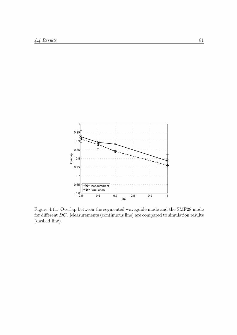
4.4 Results 81
0.5 0.6 0.7 0.8 0.9 10.6
0.65
0.7
0.75
0.8
0.85
0.9
0.95
1
DC
Overlap
Measurement
Simulation
Figure 4.11: Overlap between the segmented waveguide mode and the SMF28 modefor different DC. Measurements (continuous line) are compared to simulation results(dashed line).

82 4. Characterization techniques

5
Segmented Waveguide Taper
5.1 Introduction
As mentioned in the introduction of this thesis, insertion losses have always beena major problem in Integrated Optics. Reducing the insertion losses is importantfor telecom and sensors applications and is mandatory in the case of Quantum Com-munication where the information is carried by single photons and where amplifiersare not allowed.
Coupling losses are due to misalignments between the two waveguides, Fresnelreflection and mode mismatch. Misalignments between fiber and IO device can beavoided using careful aligning procedures. Fresnel reflection losses, due to the differ-ent values of the refractive indices of the IO waveguide and the optical fiber, can bereduced using index matching fluids or antireflection coatings at the end-face of thesample. Mode mismatch losses are due to different mode sizes in the IO waveguideand the fiber. They are particularly important in the case of active electro-optic(EO) or nonlinear (NL) devices where the component efficiency is a growing func-tion of the mode confinement. In these cases, designing the waveguide to optimizeits coupling with low confinement telecom single mode fibers is far from being op-timum, but is the more commonly used technique [105] since we are still missing apractical and cost effective solution allowing longitudinal variation of the transversalsection of the waveguide mode. This mode size transformer (taper) should be adia-batic, as short as possible, in order to realize the best trade off between propagationlosses and coupling efficiency. In the literature a lot of solutions for the design ofa taper has been proposed [106, 107, 108]. Among them, the segmented waveguideconfiguration seems the most suitable as it does not introduce additional steps inthe fabrication process [34, 109, 110, 33, 111, 112]. In principle, this technique israther general, and can be adapted to any material or waveguide fabrication tech-nique. Nevertheless, as the excess losses induced by the segmentation depend verymuch on material and waveguide fabrication technique, each case has to be carefullystudied experimentally. In this chapter, we present a study devoted to waveguides

84 5. Segmented Waveguide Taper
realized in Z-cut wafers of LiNbO3 that are commonly used for their good non-linear properties, allowing for example the fabrication of efficient optical frequencyconverters and photon pair sources required for quantum communication at telecomwavelength [113]. The reported results [114] show that when pushing the SPE pa-rameters to obtain waveguides with the maximum ∆n, which allows maximum fieldconfinement, tapers showing an overall reduction of the insertion losses with respectto the untapered waveguide can be successfully realized. The chapter is organizedas follows. In the next section, the numerical taper design are described. Then, thefabrication processes and different characterization techniques used to evaluate theimprovements of the taper are illustrated. Finally, the experimental results obtainedwith different fabrication parameters of the taper are presented.
5.2 Numerical design of the taper
The tested devices are constituted by a taper that transforms the highly confinedmode of a continuous waveguide (CWG) to that confined by a segmented one (SWG)as shown in figure 5.1. To understand the features of the mode of such a waveguide
CW SWG
W
Taper
PL
Figure 5.1: Schematic of the tested devices.
one should remind (Chapter 2) that SWG behavior can be described using theso called equivalent waveguide theorem for periodic structures [115, 116, 74]. Forwavelengths far away from the band gap, a SWG is equivalent to a continuouswaveguide with the same depth and same width but with a surface index equal to:
neq = nsub + ∆n ·DC (5.1)
where nsub is the substrate index and DC is the duty cycle. In the case of a ta-per the DC is varying from DC = 1 (continuous waveguide) to smaller DC withconstant period P so that the surface index of the equivalent waveguide is reducedas well as the mode confinement. Once the desired mode size is reached, the DCis kept constant down to the end of the sample to stabilize the mode size after thetransformation in the taper.
The numerical modelling of this structure is made with the tools presented inchapter 2. The project of all the taper parameter is obtained following the threesteps:

5.2 Numerical design of the taper 85
• Numerical modelling of continuous and segmented waveguide in Lithium Nio-bate fabricated with the SPE techniques using the mode solver and the BPMtools.
• Calculation of the best segmentation parameter (DC, P and W ) of the SWGin order to maximize the overlap between the SWG mode and the mode of astandard fiber SMF28.
• Evaluation of the taper length L and DC variation function during the prop-agation which allow an adiabatic transformation of the mode.
5.2.1 Numerical modelling of Lithium Niobate waveguides
Results presented at the end of chapter 3 show the index profile, evaluated withthe IWKB algorithm, for our planar waveguides fabricated with SPE technique inLithium Niobate substrate. This vertical index profile can be easily fitted with basicfunctions such as exponential or gaussian and used to describe the index distributioninside our numerical tools. This approach is not completely correct if the m-linesmeasurement and the IWKB profile reconstruction is made at wavelengths far fromthose of interest for the numerical analysis. In our case, in fact, the experimentalcharacterization is made at 632 nm, in order to have multimode structures, while thenumerical analysis is made at 1.55µm. Moving from λ = 632 nm to λ = 1.55 µm,in fact, dispersion changes refractive index values. The indices of the substrateand the exchanged zone vary in different ways with respect to wavelength and it isvery difficult to obtain the total dispersion behavior for a graded index waveguide.Moreover, the field at 632 nm is well confined and the interaction with the airinterface is very different with respect to the mode at 1.55 µm. These kind ofconsiderations are the base of a model proposed by Fabrizio Fogli [117](PhD studentof the university of Bologna in collaboration with the LPMC university of Nice -Sophia Antipolis). He proposed a index profile of a SPE waveguide in deep (y axis)that follows this function:
f(y) = e−( yp)
0.6
(5.2)
where p = 0.615µm has been empirically estimated .
For a planar waveguide the index distribution in the horizontal direction is con-sidered constant but for channel waveguide also lateral diffusion in the region pro-tected by the photolithography mask must be evaluated. For a z-cut Lithium Nio-bate substrate P.Aumont [71] has experimentally and numerically confirmed the

86 5. Segmented Waveguide Taper
presence of a lateral diffusion modelled by a gaussian function in this way:
g(x) =
e−
(x−W
2p
)2
, x > W2
1, W2≤ x ≤ W
2
e−
(x+ W
2p
)2
, x < W2
(5.3)
where t = 1.2 µm represents the half width at 1/e of the gaussian profile and W isthe waveguide width imposed by the photomask. Combining the vertical and thehorizontal profile, we obtain the index distribution for a continuous waveguide:
n(x, y) = ns + δnmax · f(y) · g(x) (5.4)
where ns is the substrate index and δnmax the maximum index variation at thesurface. For a well confined waveguide δnmax has been estimated equal to 0.071.This structure can be analyzed with the mode solver. Figure 5.2 shows the intensityof the fundamental mode at 1.55 µm for the three components Ey and Ex and Ez
(Ey is the main component).
Figure 5.2: Three electric field components of the SPE waveguide calculated withthe mode solver.
The computational window is 60 µm × 50 µm, large enough to prevent bordereffects induced by the absence of PML. The mesh discretization has been fixed at

5.2 Numerical design of the taper 87
∆x = ∆y = 0.2 µm as the best trade off between the accuracy of the results andthe computational time has been obtained for that mesh as shown in the next table.This model is in quite good agreement with the m-lines measurement performed at
∆x = ∆y x points y points neff Elapsed time [s] Precision0.05 600 800 2.1435705 3360 ref.0.1 300 400 2.1427007 240 4.06e-40.2 150 200 2.1424178 35 5.38e-40.4 75 100 2.1422174 5 6.32e-40.5 60 80 2.1419813 2 7.42e-4
1.55 µm with just one mode is in propagation. Once the mode guided by the straightwaveguide has been calculated, it is possible to model the segmented waveguidebehavior. The Beam Propagation Method is the best numerical tool to analyzethis kind of longitudinal varying structure. The fundamental assumptions to obtaincorrect BPM solutions are satisfied for SPE : LiNbO3 waveguides, in fact, theindex variation is weak and the field intensity can not change very fast during thepropagation on distance compared to the wavelength. Moreover, the low contrastlongitudinal changes do not allow the excitation of back propagating modes.
In view of realistic simulations of these waveguides, the refractive index modellinginclude both the effects of lateral and longitudinal proton diffusion. As we use Z-cutLithium Niobate crystal substrate, we can say that lateral and longitudinal diffusionare identical and induce the same index profile. The profile can than be written inz direction as:
h(z) =
e−( zt )
2
, z < zi
e−( z−zit )
2
, zi ≤ z < 2zi
1, P (1−DCm) ≤ z < P
(5.5)
where zi is the the point corresponding to the mid masked zone. Moreover DCm isthe mask duty cycle defined as the ratio between the length of the mask segment andthe period. Adopting the longitudinal index profile of equation 5.5 Pierre Aumont[71] in his PhD work calculated the transmission in the SPE segmented waveguides,concluding that the reflections in the Brag region are extremely weak for periodslarger than 8µm, due to the strong lateral diffusion of the fabrication process. Notethat, if the segments were square like shape, then the high order contribution ofthe refractive index grating formed by the segments could be efficient. But becauseof the strong lateral diffusion, the segments are not at all square like shape butmuch more smooth, so the high orders are extremely unefficient. For example, in awaveguide with length equal to 2.5cm, P = 8µm, the nearest Bragg peak at wave-length 1.55µm reduces the transmission from 1 to 0.9997 which is not a detectable

88 5. Segmented Waveguide Taper
variation. With the same structure, the length of the waveguide should be 14cm inorder to obtain a 1% attenuation. In our PSW the periods are always larger than8µm and the reflectivity can only be smaller. For this reason we have no limitationon the device operating bandwidth and we could use the BPM to study this kind ofstructure.In case of intersection between two neighboring gaussian profiles, each profile is con-sidered independently as depicted in figure 5.3. This choice has been made by PierreAumont comparing the effective index measurements obtained with simulations atdifferent index profiles and different DCm. An important consequence derived by
0 2 4 6 8 10 12 14 16 18 200
0.2
0.4
0.6
0.8
1
z [mm]
h(z
)
zi P
Figure 5.3: Longitudinal refractive index profile for a SPE segmented waveguidewith perios P = 10 µm and DCm = 0.7.
the presence of a longitudinal diffusion is that the DC must be redefined as:
DC =
P∫0
h(z)dz
P∫0
1dz
(5.6)
which, after some algebra, becomes:
DC = DCm +√
πt
Perf
[P (1−DCm)
2t
](5.7)
which can be useful when using the equivalent waveguide theorem. When we intro-duce this segmented waveguide model in the 3D BPM we can use the same mesh usedin the mode solver. Concerning the longitudinal step, we have fixed ∆z = 0.2 µm.This value has been chosen as before as the best compromise between precision andCPU time which is proportional, for a fixed propagation length, to the inverse of∆z. The following table shows the computational times for different values of ∆z

5.2 Numerical design of the taper 89
and the corresponding precisions obtained for the power evolution in a 2mm lengthsegmented waveguide with P = 15µm, W = 5µm and DCm = 0.5. I consider theresult obtained for ∆z = 0.1µm as a reference (Ref. in the table) for the precisionevaluation.
∆z[µm] Elapsed time [s] Precision0.1 14520 Ref.0.2 7260 5.68e-50.4 4020 2.84e-40.5 3360 4.26e-41.0 2340 1.82e-3
5.2.2 Segmented waveguide design
The SWG positioned at the end of the sample determines the dimensions of theoutput mode. Modifying its parameters (DC, P and W ) we can then improve thecoupling efficiency to the fiber mode.
The parameter we need to maximize is the overlap integral between the outputfield of the SWG ψSWG and the fiber mode ψf , defined as:
I =
∣∣∫∫ ΨSWG ·Ψ∗fdS
∣∣2∫∫ |ΨSWG|2 dS · ∫∫ |Ψf |2 dS
. (5.8)
The fiber mode ψf can be easily obtained using the mode solver because the structureis z-invariant. Considering a standard SMF28 single mode fiber [?] the result isshown in figure 5.4.
Figure 5.4: Calculated fundamental mode intensity in a standard SMF28.
In order to obtain a good precision when determining the propagating field inthe segmented waveguide, instead of the mode solver, we have used the 3D BPM.The transversal model of the integrated waveguide is the same of the previous model
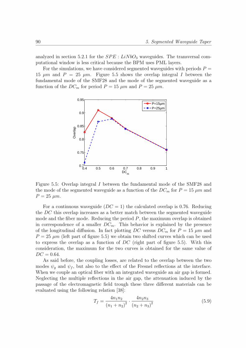
90 5. Segmented Waveguide Taper
analyzed in section 5.2.1 for the SPE : LiNbO3 waveguides. The transversal com-putational window is less critical because the BPM uses PML layers.
For the simulations, we have considered segmented waveguides with periods P =15 µm and P = 25 µm. Figure 5.5 shows the overlap integral I between thefundamental mode of the SMF28 and the mode of the segmented waveguide as afunction of the DCm for period P = 15 µm and P = 25 µm.
0.4 0.5 0.6 0.7 0.8 0.9 10.7
0.75
0.8
0.85
0.9
0.95
DCm
Ove
rlap
P=15µmP=25µm
Figure 5.5: Overlap integral I between the fundamental mode of the SMF28 andthe mode of the segmented waveguide as a function of the DCm for P = 15 µm andP = 25 µm.
For a continuous waveguide (DC = 1) the calculated overlap is 0.76. Reducingthe DC this overlap increases as a better match between the segmented waveguidemode and the fiber mode. Reducing the period P , the maximum overlap is obtainedin correspondence of a smaller DCm. This behavior is explained by the presenceof the longitudinal diffusion. In fact plotting DC versus DCm for P = 15 µm andP = 25 µm (left part of figure 5.5) we obtain two shifted curves which can be usedto express the overlap as a function of DC (right part of figure 5.5). With thisconsideration, the maximum for the two curves is obtained for the same value ofDC = 0.64.
As said before, the coupling losses, are related to the overlap between the twomodes ψg and ψf , but also to the effect of the Fresnel reflections at the interface.When we couple an optical fiber with an integrated waveguide an air gap is formed.Neglecting the multiple reflections in the air gap, the attenuation induced by thepassage of the electromagnetic field trough these three different materials can beevaluated using the following relation [38]:
Tf =4n1n2
(n1 + n2)2 ·
4n2n3
(n2 + n3)2 (5.9)
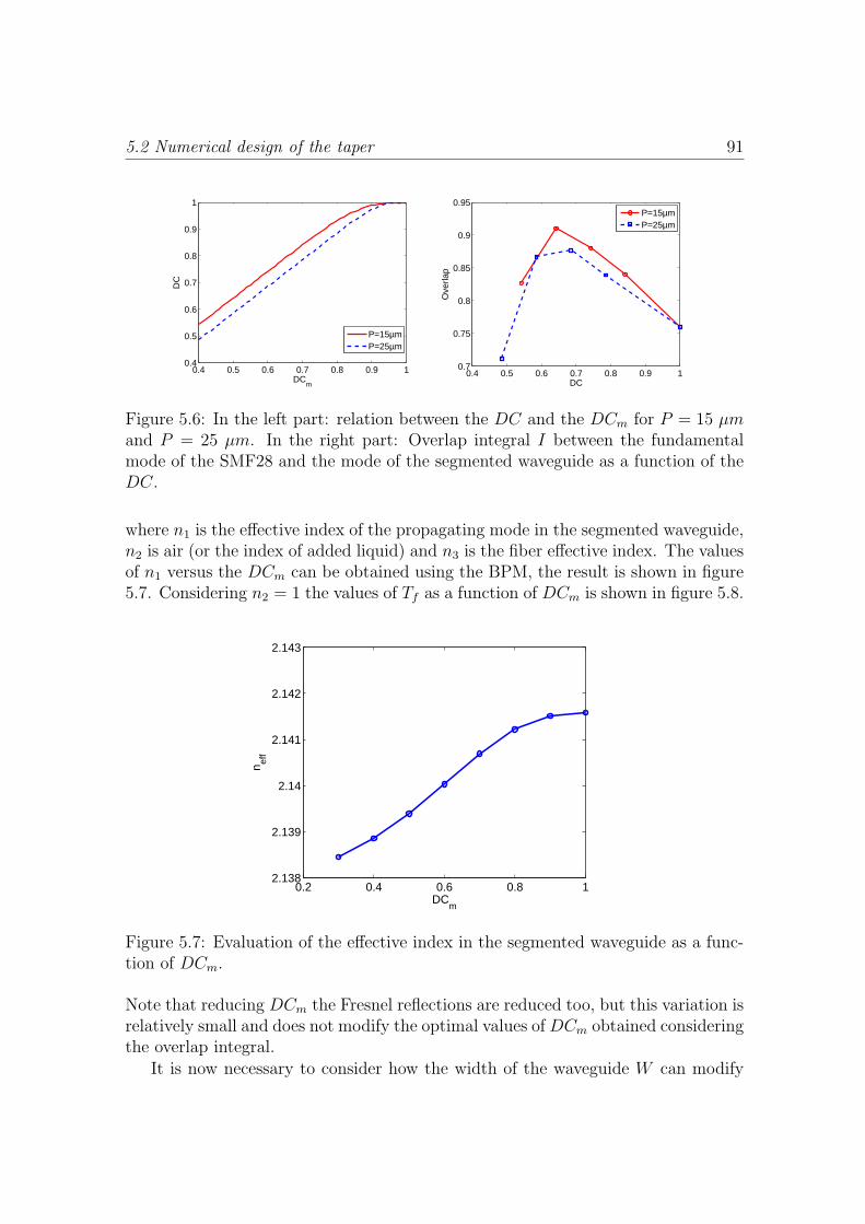
5.2 Numerical design of the taper 91
0.4 0.5 0.6 0.7 0.8 0.9 10.4
0.5
0.6
0.7
0.8
0.9
1
DCm
DC
P=15µmP=25µm
0.4 0.5 0.6 0.7 0.8 0.9 10.7
0.75
0.8
0.85
0.9
0.95
DC
Ove
rlap
P=15µmP=25µm
Figure 5.6: In the left part: relation between the DC and the DCm for P = 15 µmand P = 25 µm. In the right part: Overlap integral I between the fundamentalmode of the SMF28 and the mode of the segmented waveguide as a function of theDC.
where n1 is the effective index of the propagating mode in the segmented waveguide,n2 is air (or the index of added liquid) and n3 is the fiber effective index. The valuesof n1 versus the DCm can be obtained using the BPM, the result is shown in figure5.7. Considering n2 = 1 the values of Tf as a function of DCm is shown in figure 5.8.
0.2 0.4 0.6 0.8 12.138
2.139
2.14
2.141
2.142
2.143
DCm
n eff
Figure 5.7: Evaluation of the effective index in the segmented waveguide as a func-tion of DCm.
Note that reducing DCm the Fresnel reflections are reduced too, but this variation isrelatively small and does not modify the optimal values of DCm obtained consideringthe overlap integral.
It is now necessary to consider how the width of the waveguide W can modify

92 5. Segmented Waveguide Taper
0.2 0.4 0.6 0.8 10.8397
0.8398
0.8399
0.84
0.8401
0.8402
DCm
Tf
Figure 5.8: Fresnel transmission coefficient versus DCm considering a segmentedwaveguide coupled to a fiber optic trough an air gap.
the overlap with the fiber mode. To do that, we have considered the parameterswhich provide the best performance DCm = 0.5 and P = 15 µm and we haveevaluated the overlap integral I varying W . Figure 5.9 shows the obtained results.For W < 3.5 µm the waveguide mode approaches the cutoff condition and for W >
3 4 5 6 7 80.85
0.86
0.87
0.88
0.89
0.9
0.91
W [µm]
Ove
rlap
Figure 5.9: Overlap integral versus the waveguide width (W ).
8 µm the mode presents a strong ellipticity and the waveguide becomes multimode.For 3.5 < W < 8 µm the overlap variation is not very large and the maximum isobtained for W = 5 µm.
Another important parameter, we would like to calculate with the BPM analysis,

5.2 Numerical design of the taper 93
is the propagation loss. This evaluation can be easily done calculating the totalpower of the computational window during the propagation and fit the result with anexponential. Such kind of evaluation has been made for the segmented waveguideswith period P = 15 µm, W = 5 µm for different DCm. The obtained resultshas then been compared to the measured propagation losses presented in chapter3. From figure 5.10 we note disagreement between the two results. This happen
0.5 0.6 0.7 0.8 0.9 10
0.5
1
1.5
2
DCm
Loss
es [d
B/c
m]
MeasurementSimulation
Figure 5.10: Comparison between calculated and measured propagation losses as afunction of DCm for segmented waveguides with period P = 15 µm and W = 5 µm.
because we can not consider in the BPM model the roughness at the surface of thereal component. A proposed solution is to introduce complex dielectric constantin the BPM and assign an absorption profile to the waveguide. The problem is todetermine the right complex profile for which the scattering losses are equal to theartificial absorption losses.
The concluding of this discussion on segmented waveguides design, we have foundthat the best coupling with a SMF28 can be obtained for P = 15 µm, DCm = 0.5and W = 5 µm.
5.2.3 Taper design
In this section we will now address the problem of designing a tapered SWG.The aim of the taper is to transform (see figure 5.11) the fundamental mode of acontinuous waveguide into the fundamental mode of the segmented waveguide thatprovides the best coupling with the mode fiber. As expressed by the equivalentwaveguide theorem, the DC is the parameter we have to change in order to modifythe segmented waveguide properties. This parameter can be modified playing withDCm and P . With the design of the final PSW (positioned at the interface with the

94 5. Segmented Waveguide Taper
fiber), we have fixed the parameters W , DCm and P at the end of the taper. Theoptimal W of the PSW is equal to 5µm, which is a good value also for a continuouswaveguide. For this reason we do not need to modify its value in the taper. In thecase of continuous waveguide which requires different values of W a variation of thetaper width should be introduced. For the mode shaping we can play with bothDCm and P . If we choose to modify P we have two possible choices:
1. Move from a continuous waveguide to a PSW with DCm constant;
2. Move from a continuous waveguide to a PSW modifying both DCm and P .
Solution 1 has the problem that for DC near to 1, P must reach higher values andthis causes the increase of the total taper length (and of losses accordingly). Solution2 has not the problem of solution 1 but the taper design results rather complicatedas both DCm and P must change in order to obtain a slow variation of the real DC.In conclusion, the best taper design is obtained modifying the DCm with a constantperiod P .
Waveguide
Figure 5.11: Schematic representation of the taper structure for the mode transfor-mation.
The 3D BPM has been used also for the taper analysis. The goal of the taper is toperform such mode transformation minimizing losses and device length. Taper lossesare due to two contributions. The firmer is related to the fact that the structureis z-variant and during mode transformation some radiating modes can be excitedthus increasing the propagation losses. This problem, in our case, is increased byfabrication imperfection and for this reason it is very difficult to quantify their values.The latter contribution is related to the mismatch between the mode at the outputof the taper and the mode of the segmented waveguide, as it happens in a generalcoupling problem.
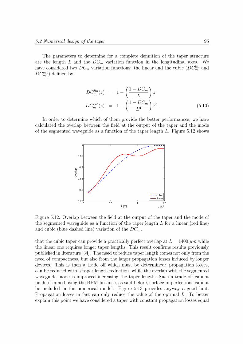
5.2 Numerical design of the taper 95
The parameters to determine for a complete definition of the taper structureare the length L and the DCm variation function in the longitudinal axes. Wehave considered two DCm variation functions: the linear and the cubic (DC lin
m andDCcub
m ) defined by:
DC linm (z) = 1−
(1−DCm
L
)z
DCcubm (z) = 1−
(1−DCm
L3
)z3. (5.10)
In order to determine which of them provide the better performances, we havecalculated the overlap between the field at the output of the taper and the modeof the segmented waveguide as a function of the taper length L. Figure 5.12 shows
0 0.5 1 1.5
x 10−3
0.75
0.8
0.85
0.9
0.95
1
z [m]
Ove
rlap
cubiclinear
Figure 5.12: Overlap between the field at the output of the taper and the mode ofthe segmented waveguide as a function of the taper length L for a linear (red line)and cubic (blue dashed line) variation of the DCm.
that the cubic taper can provide a practically perfect overlap at L = 1400 µm whilethe linear one requires longer taper lengths. This result confirms results previouslypublished in literature [34]. The need to reduce taper length comes not only from theneed of compactness, but also from the larger propagation losses induced by longerdevices. This is then a trade off which must be determined: propagation losses,can be reduced with a taper length reduction, while the overlap with the segmentedwaveguide mode is improved increasing the taper length. Such a trade off cannotbe determined using the BPM because, as said before, surface imperfections cannotbe included in the numerical model. Figure 5.13 provides anyway a good hint.Propagation losses in fact can only reduce the value of the optimal L. To betterexplain this point we have considered a taper with constant propagation losses equal

96 5. Segmented Waveguide Taper
to 2.5 dB/cm. Figure 5.13 shows the propagation and the overlap losses and theircombination to obtain the total losses as a function of the length L. Note that the
2 4 6 8 10 12 14
x 10−4
2
4
6
8
10
12
14
16
18
20
Taper length [m]
Loss
es [%
]
Overlap lossesPropagation lossesTotal
Figure 5.13: Propagation (green dotted line) and overlap losses (blue dashed line)as a function of the taper length L. The red line represents the total of the twocontributes.
length of the total losses minimum (red line) is no longer 1400 µm but reduced to1190 µm once the propagating losses term is considered. In conclusion the numericalanalysis of the taper shows that changing the DCm from DCm = 1 to DCm = 0.5with a segmentation period P = 15 µm, the better solution is to use a cubic DCm
longitudinal variation function and a length between 1000 and 1400 µm, dependingon the propagating losses. The overlap with the SMF28 pass from 76% to 92%(0.82 dB) and from this improvement we must subtract the loss introduced by thetaper and the segmented waveguide respect the continuous waveguide. The worstcase of taper losses equal to 2.5 dB/cm induce a reduction of 0.36 dB but morereasonably we can imagine a reduction between 0.1 dB and 0.2 dB, which allow aninsertion losses overall reduction between 0.62 dB and 0.72 dB.
To conclude the numerical analysis we can study the wavelength dependence ofthe optimum design for improved coupling with SMF28. Modifying the workingwavelength, at the output of the taper, the mode shape changes in a different wayrespect to the fiber mode. This means that, in order optimize the taper designfor different wavelengths, its parameters must be recalculated. We have done somesimulations for λ = 1.31µm instead of 1.55µm. With such a wavelength reduction,at the output of the taper, the mode size is strongly reduced with respect to the fiber.The next table shows the overlap as a function of the DCm for period P = 15µmand W = 5µm at λ = 1.31µm.
Note that the maximum value of the overlap is now obtained for DCm = 0.4 andits value is smaller with respect the overlap of 0.92 calculated at λ = 1.55µm andDCm equal to 0.5. It is possible to conclude that with a wavelength reduction, the

5.3 Device Fabrication 97
DCm Overlap0.3 0.87560.4 0.89500.5 0.8366
optimum design can be obtained reducing the final DCm of the segmented waveguidetaper and similarly with a wavelength increase the optimum design can be obtainedfor higher DCm. Concerning the taper length no important variations have beenobserved in this wavelength range.
5.3 Device Fabrication
Samples are fabricated on a Z-cut LiNbO3 substrate with the SPE and pho-tolithography techniques described in chapter 3. The SPE has been used with twodifferent values of LB percentage. A first sample has been fabricated with 3.5%of LB, which gives a small index variation and a second one with 2.8% of LB tocreate SPE guides with the maximum index variation. In both cases waveguides aremonomode at 1.55 µm, the standard telecommunication wavelength and thereforethe preferred wavelength for long distance quantum communications. As said be-fore, the parameters we can choose when designing the taper are its length (L), thesegmentation period (P ), the final duty cycle (DCm) and the waveguide width (W ).Tapers with 48 possible combinations of these parameters were then fabricated onthe same substrate. The following table summarizes the values of the parametersused for the tapers present on the sample.
P [µm] DCm W [µm] L[µm]15 0.5 5 10025 0.6 7 600
0.7 10001400
The last fabrication step is the end-face polishing to allow end-fire coupling of thesample with the input and output fiber. A particular care is devoted to the controlof the angle between the end-face and the waveguides which has to be 90 in orderto use the Fabry-Perot technique to measure propagation loss [83].
5.4 Experimental setup
In this section, we describe the device characterizations of the fabricated samplesusing the experimental setup described in chapter 4. This system can be used notonly to evaluate separately the integrated optical waveguide propagation losses and

98 5. Segmented Waveguide Taper
the mode overlap integral but also their combined effect, comparing the overall cou-pling efficiencies using tapered and untapered structures. The three characterizationsteps can be summarized as follows:
• The propagation losses are measured using the Fabry-Perot cavity technique[83]. Measuring the power transmitted through the system at different wave-lengths, one obtains fringes whose contrast is directly related to the propaga-tion losses.
• The overlap integral between waveguide and fiber modes can be evaluated viathe measurement of the mode cross-correlation. Such a function is measuredby exciting the waveguide under test with a constant power at a fixed wave-length and recording the power collected by the output fiber, while it scans,with 16 nm steps, a 25 µm × 25 µm window centered on the waveguide out-put. Such measurement is similar to that described in [99] and provides manyinformation. First of all we can quantify how critical the fiber to waveguidealignment is. A sharp cross-correlation function corresponds to a low toler-ance to alignment errors, while a smooth cross correlation function allows somealignment errors without dramatic impact on the coupling losses. Moreover,knowing the cross-correlation function and the fundamental mode pattern ψf
of the SFM28 fiber, it is possible to reconstruct the waveguide mode field dis-tribution ψw through a simple deconvolution operation. This finally allowsevaluating the intensity overlap integral 5.8. Evaluating this integral for dif-ferent tapers allows then to determine the combination of parameters whichgives the better mode matching.
• The overall coupling efficiency improvement, which depends on the combinedeffect of taper induced propagation losses and waveguide to fiber mode match-ing improvement can be evaluated comparing the maximum power transmittedthrough the different waveguides present on the sample under test. For eachwaveguide, the throughput power is measured optimizing contemporarily thepositions of both input and output fibers with piezo-controlled stages.
5.5 Results
We have first characterized the sample obtained with 3.5% of LB. Figure 5.14(a)presents the mode size as a function of the DCm of the segmented waveguides. ForDCm = 1, corresponding to a continuous waveguide, we found mode sizes biggerthan the fiber mode size (dashed line). This indicates that the field is less confinedin the waveguide than in the fiber. In this case we found an overlap of 85%, whichcannot be improved by the use of a taper. The losses measured for the continuouswaveguide are 1.5 dB/cm. They are mainly caused by surface scattering. The weak

5.5 Results 99
0.5 0.6 0.7 0.8 0.9 10
2
4
6
8
10
12
14
16
18
20
DCm
Mo
de
siz
e [mm
]SMF28
Lateral mode size
Vertical mode size
(a)
0.5 0.6 0.7 0.8 0.9 10
2
4
6
8
10
12
DCm
Mo
de
siz
e [mm
]
SMF28
Lateral mode size
Vertical mode size
(b)
Figure 5.14: Measurement of the lateral and vertical mode sizes (at 1/e of thefield maximum) of segmented waveguides as a function of DCm with W = 5µm andP = 15µm for two samples fabricated with 3.5% (a) and 2.8% (b) of LB. The dottedline refers to the mode size of the output fiber SMF28.
confinement of the mode allows a strong interaction with surface imperfections andis responsible for these rather high scattering losses. In this case high performancescannot reasonably be obtained for non-linear or electro-optical components. In fact,even if coupling losses are small, the weak mode confinement does not allow stronglocalized field intensity.
The second sample was fabricated performing SPE with 2.8% of LB, conditionwhich corresponds to the maximum index increase achievable with this technique. Inthis case a stronger confinement is expected. This is confirmed by the results shownin Figure 5.14(b), where the mode size of the segmented waveguide is reported asa function of the DCm. The field is more confined and this contributes to reducethe losses down to 1 dB/cm. As said before, the drawback of a smaller mode sizeis the increase of the coupling losses related to the reduction of the mode-fiber

100 5. Segmented Waveguide Taper
overlap. Figure 5.15 shows that for DCm = 1 the overlap is 78% but the use of asegmented waveguide taper can improve it up to 92% for DCm = 0.5, W = 5 µmand a period P = 15 µm (continuous line). This corresponds to an improvementof 0.71 dB in logarithmic scale. This experimental result agrees with the numericalprediction obtained using a 3D BPM [35] (dashed line in figure 5.15). However,this result is not the real performance improvement, which can be obtained usingtapered and segmented waveguides, as they induce extra propagation losses whichare not taken into account in the overlap integral. These extra propagation lossesare due to imperfect mode transformation and scattering losses at the segmentsedges. So, the use of a segmented waveguide taper becomes effective if the modematching improvement is larger than the propagation loss increase. Using the Fabry-Perot cavity technique, illustrated in the previous section, taper and segmentedwaveguide introduction was found to cause a loss increase of only 0.04dB withrespect to the continuous waveguide. The total improvement obtained in termsof waveguide to fiber coupling is then 0.71 − 0.04 = 0.67 dB. The precision ofthis result is estimated to be around ±0.2 dB. The overall improvement was alsomeasured using the approach described in chapter 4. The results are reported in thefollowing table where Pt and PCWG are output powers measured at the end of thewaveguides with and without taper respectively. Negative results correspond to thecases where the overlap improvement does not even compensate for the additionallosses. The optimum length of the taper depends on the segmentation parametersand the table reports the results for the lengths that provide the best performances.We obtained the overall best result with a 1400 µm long taper associated to a2600µm long segmented waveguide, with P = 15 µm, W = 5 µm and DCm = 0.5.In that case, an overall increase of 0.78 dB of the transmitted power was observedwith respect to the continuous waveguide. The precision of this measurement isaround ±0.1 dB. These two different measurements give results, which taking intoaccount the uncertainties, are equal and confirm the practical interest of segmentedwaveguide tapers realized using the SPE process. It is worth noting that the teststructures realized for this study have taper at one end only. Therefore, the benefitfor a real component with a taper at both ends will be doubled. Further improvementcan also be obtained working on the taper length, which can be reduced by reducingthe segmentation period.
Taper length 10 log(Pt/PCWG) 10 log(Pt/PCWG)P [µm] L[µm] DCm [W = 5µm] [W = 7µm]
1400 0.5 0.78 dB 0.06 dB15 1000 0.6 0.22 dB -0.25 dB
600 0.7 0.19 dB 0.20 dB1400 0.5 -0.53 dB 0.37 dB
25 1400 0.6 0.15 dB 0.43 dB600 0.7 0.51 dB 0.47 dB
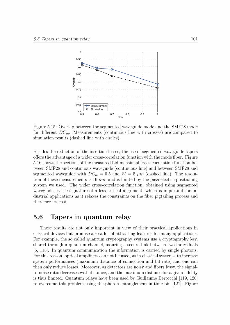
5.6 Tapers in quantum relay 101
0.5 0.6 0.7 0.8 0.9 10.6
0.65
0.7
0.75
0.8
0.85
0.9
0.95
1
DCm
Overlap
Measurement
Simulation
Figure 5.15: Overlap between the segmented waveguide mode and the SMF28 modefor different DCm. Measurements (continuous line with crosses) are compared tosimulation results (dashed line with circles).
Besides the reduction of the insertion losses, the use of segmented waveguide tapersoffers the advantage of a wider cross-correlation function with the mode fiber. Figure5.16 shows the sections of the measured bidimensional cross-correlation function be-tween SMF28 and continuous waveguide (continuous line) and between SMF28 andsegmented waveguide with DCm = 0.5 and W = 5 µm (dashed line). The resolu-tion of these measurements is 16 nm, and is limited by the piezoelectric positioningsystem we used. The wider cross-correlation function, obtained using segmentedwaveguide, is the signature of a less critical alignment, which is important for in-dustrial applications as it relaxes the constraints on the fiber pigtailing process andtherefore its cost.
5.6 Tapers in quantum relay
These results are not only important in view of their practical applications inclassical devices but promise also a lot of attracting features for many applications.For example, the so called quantum cryptography systems use a cryptography key,shared through a quantum channel, assuring a secure link between two individuals[6, 118]. In quantum communication the information is carried by single photons.For this reason, optical amplifiers can not be used, as in classical systems, to increasesystem performances (maximum distance of connection and bit-rate) and one canthen only reduce losses. Moreover, as detectors are noisy and fibers lossy, the signal-to-noise ratio decreases with distance, and the maximum distance for a given fidelityis thus limited. Quantum relays have been used by Guillaume Bertocchi [119, 120]to overcome this problem using the photon entanglement in time bin [121]. Figure

102 5. Segmented Waveguide Taper
-15 -10 -5 0 5 10 150
0.1
0.2
0.3
0.4
0.5
0.6
0.7
0.8
0.9
1
Lateral offset [mm]
Norm
alized inte
nsity
DCm=0.5
DCm=1
(a)
-15 -10 -5 0 5 100
0.1
0.2
0.3
0.4
0.5
0.6
0.7
0.8
0.9
1
Vertical offset [mm]
Norm
alised inte
nsity
DCm=0.5
DCm=1
(b)
Figure 5.16: Lateral (a) and vertical (b) section of bidimensional cross-correlationfunction between SMF28 and continuous waveguide (continuous line) and betweenSMF28 and segmented waveguide (dashed line) with P = 15µm,W = 5µm andDCm = 0.5.
A BRQuantum channel
Trigger
Figure 5.17: Quantum communication system with relay.
5.17 shows a schematic representation of the system. A is the photon source. Whena single photon is transmitted on the quantum channel a second electrical triggeris launched too. In order to the maximum allowed distance between A and Ba quantum relay R is placed before the receiver B. The quantum relay is based
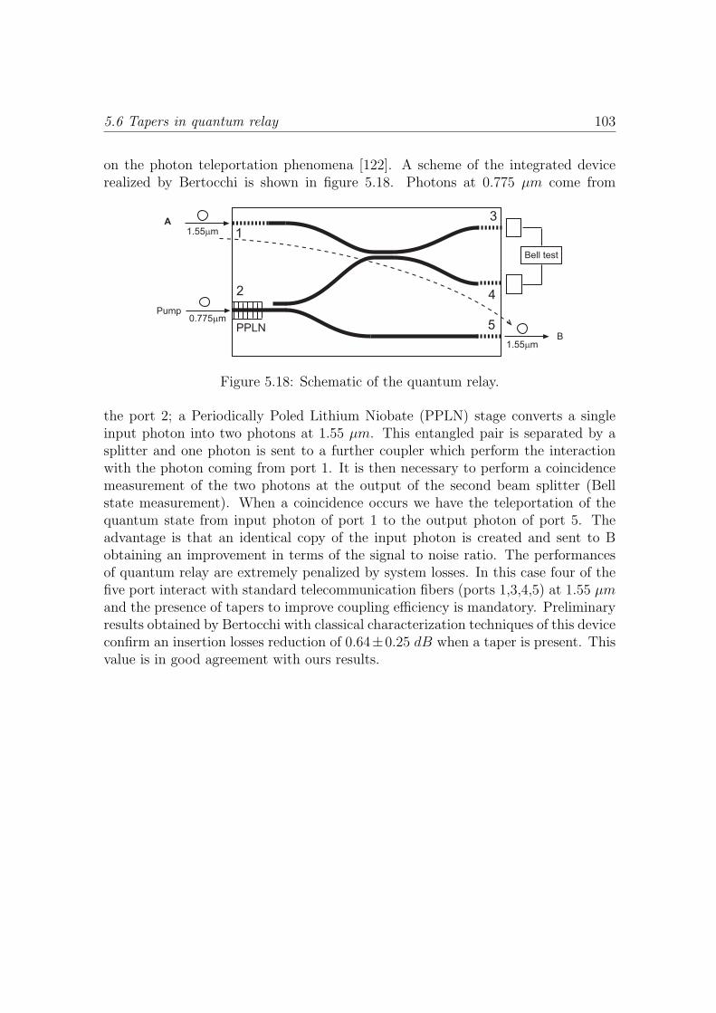
5.6 Tapers in quantum relay 103
on the photon teleportation phenomena [122]. A scheme of the integrated devicerealized by Bertocchi is shown in figure 5.18. Photons at 0.775 µm come from
PPLN
1
2
1.55mm
0.775mm
1.55mm
Bell test
Pump
A
B
3
4
5
Figure 5.18: Schematic of the quantum relay.
the port 2; a Periodically Poled Lithium Niobate (PPLN) stage converts a singleinput photon into two photons at 1.55 µm. This entangled pair is separated by asplitter and one photon is sent to a further coupler which perform the interactionwith the photon coming from port 1. It is then necessary to perform a coincidencemeasurement of the two photons at the output of the second beam splitter (Bellstate measurement). When a coincidence occurs we have the teleportation of thequantum state from input photon of port 1 to the output photon of port 5. Theadvantage is that an identical copy of the input photon is created and sent to Bobtaining an improvement in terms of the signal to noise ratio. The performancesof quantum relay are extremely penalized by system losses. In this case four of thefive port interact with standard telecommunication fibers (ports 1,3,4,5) at 1.55 µmand the presence of tapers to improve coupling efficiency is mandatory. Preliminaryresults obtained by Bertocchi with classical characterization techniques of this deviceconfirm an insertion losses reduction of 0.64±0.25 dB when a taper is present. Thisvalue is in good agreement with ours results.

104 5. Segmented Waveguide Taper
6
Segmented waveguide mode filter
6.1 Introduction
In this chapter a further application of segmented waveguides will be presented:the so called mode filters. These devices eliminate the higher order modes propagat-ing in a multimode waveguide. They can be used, for example, in frequency conver-sion applications based on non linear effects, where a pump at a lower wavelengthshould interact with a signal to generate an idler with a new wavelength. Usually thewaveguide becomes multimode at the pump frequency and the contribution of thehigher order modes can perturb the output spectrum. After illustrating the workingprinciples of these devices and a simple model based on the Couple Mode Theorywhich proved very useful both for device design and analysis, some results provingthe good performances of these devices will be presented and discussed [123].
6.2 Mode filter operation
Using the equivalent waveguide theorem for segmented waveguides we can arguethat it is possible to tailor the device characteristics in such a way that if manymodes are propagating in a waveguide, only the fundamental mode is preserved,while all the other modes are led to cutoff. That theorem suggests in fact thatthe cutoff wavelength of the propagating mode can be reduced by modifying theDC [19]. Figure 6.1, shows the cutoff wavelengths of the fundamental and the firsthigher order modes as a function of the DC of the segmented waveguide. Assuming,for example, a working wavelength of 0.85 µm, one can see that, for DC < 0.39, thehigher order mode is no longer guided, while the fundamental one still propagatesuntil the DC becomes 0.29.
So, for a fixed wavelength, it is then possible to determine the DC intervalfor which only the fundamental mode can propagate. The transition between themultimode continuous waveguide to the segmented waveguide and vice versa can not

106 6. Segmented waveguide mode filter
0 0.2 0.4 0.6 0.8 10
0.2
0.4
0.6
0.8
1
1.2
1.4
1.6
DC
l0cu
toff
[mm
]
Higher order mode
Fundamental mode
Figure 6.1: Cutoff wavelength for two modes of a segmented waveguide as a functionof the duty cycle DC.
be abrupt but tapered to minimize losses. Moreover, in this case, the taper avoidsthe formation of unwanted higher order mode after the filtering process. A rapidtransformation after the segmented waveguide can excite once again the modes ofthe multimode structure making useless the filter.
A schematic representation of a mode filter based on segmented waveguides pro-posed by Chou et all. [34] is shown in figure 6.2. In this solution, the segmentedwaveguide (SWG), which works as a mode filter, is placed at the entrance of the sam-ple in order to obtain the double advantage of filtering the higher order modes andalso of improving the overlap between the external mode fiber and the fundamentalmode of the segmented waveguide.
TAPER WaveguidePSW
Figure 6.2: Schematic representation of a mode filter based on segmented waveguideproposed by Chou et al. [34].
The experimental results presented by Chou et all. are interesting, but in their
6.3 Coupled Mode Theory for segmented waveguide mode filters 107
work the rules used for the taper design are not discussed. Knowledge of these rulewould be important for best design and minimization of the excitation of the higherorder mode. For this reason, we have developed a model based on the coupled modetheory (CMT) and the equivalent waveguide theorem able to study the couplingphenomena inside a segmented waveguide taper. This allows to predict the behaviorof the taper and to fix its parameters to obtain the desired features.
6.3 Coupled Mode Theory for segmented wave-
guide mode filters
A continuous straight dielectric waveguide transmits any of its guided modeswithout coupling their energy to any other guided or radiation mode, as modesare mutually orthogonal [37]. It is possible to extend this orthogonality conditionfor modes of ideal segmented waveguide [24]. But any imperfection of the wave-guide, such as a local change of its refractive index destroys the condition of perfectstraightness or an imperfection of the interface between two regions with differentrefractive index of a segmented waveguide couples modes each other (guided andradiation). Imperfections of this type are unavoidable.
In our case both unwanted imperfections and segmentations with variable DCare present. Then, the modes that propagates trough a taper are not orthogonaland coupling phenomena occurs. The coupled mode theory (CMT) [38] can be usedto understand how to design a taper in order to reduce the excitation of higher ordermodes. Such a theory is based on some simplifying assumptions. Usually, we callunperturbed structure, the structure for which we know a complete set of solutions,for example the continuous waveguide. Then, we consider a second structure, theso called perturbed structure, which is very similar to the unperturbed one, but withunknown solutions. In our case this second structure is the taper with imperfections.This second structure can be obtained modifying the unperturbed one by a physicalor geometrical parameter that we call ∆ε defined as the difference between thedielectric distribution for the two structures. In the following we indicate with suffix1 the unperturbed solutions, while we use the suffix 2 for the perturbed solutions. Inharmonic regime and without sources, the Maxwell equations for the unperturbedstructure can be written as:
∇× E1 = −jωµH1
∇×H1 = jωεE1 (6.1)
while, in the case of perturbed structure, they become:
∇× E2 = −jωµH2
∇×H2 = jω(ε + ∆ε)E2. (6.2)

108 6. Segmented waveguide mode filter
Indicating with (Eν(x, y), Hν(x, y)) the complete set of solutions for the unperturbedstructure, considering only small perturbations, it can also be assumed that, theunknown field of the perturbed structure can be expressed as:
E2t(x, y, z) =∑
ν
(aν + bν)Etν(x, y) (6.3)
H2t(x, y, z) =∑
ν
(aν − bν)H tν(x, y) (6.4)
where the unknown coefficients:
aν(z) = Aν(z) e−jβνz (6.5)
bν(z) = Bν(z) ejβνz (6.6)
refer to the modes, which propagate in the positive direction and negative directionof the z axis. Note also that the mode propagation constants are assumed not todepend on the propagation coordinate z because of the small perturbations, whilethe mode amplitude depends on z as we are looking for coupling effects.
For simplicity we will assume also that no radiation mode is considered (this iscompatible with the hypothesis of small perturbations) and that only two guidedmodes can propagate. After some well known algebra (see for example [38]) theequations to be solved to determine the unknown amplitude coefficients are foundto be:
dA1
dz= −jκA2 e−j(β2−β1)z
dA2
dz= −jκ∗A1 e−j(β1−β2)z (6.7)
where
κ =ω
4
∫ ∫ ∞
−∞∆ε Etν · E∗
tµ dx dy (6.8)
is the so called coupling coefficient between the transversal component of the modeof the perturbed structure Etµ and the ν-th mode of the unperturbed structure. Inour case the only value to consider for ν and µ are for both of them 1 and 2.
The solution of the equations 6.7 is:
A1 = ej ∆β2
z ·(A′1e
jSz + A′′1e−jSz
)
A2 = e−j ∆β2
z ·(A′2e
jSz + A′′2e−jSz
)(6.9)
where
∆β = β1 − β2 (6.10)
6.3 Coupled Mode Theory for segmented waveguide mode filters 109
Type ParameterDepth profile Exponential 2.2 µm (@1/e)Width profile Gaussian 3 µm (@1/e)δn 0.018
Table 6.1: Parameters of the refractive index profiles used to calculate ∆β.
and S is defined as:
S =
√(∆β
2
)2
+ |κ|2. (6.11)
Constants A′1,A
′′1 ,A
′2 and A
′′2 can be determined imposing the initial exciting condi-
tion for the two modes. The taper is placed after the mode filter and for this reasonthe power of the higher order mode is zero A2(z = 0) = 0 and all the power is inthe fundamental one. The guided powers of the two modes in the taper are foundto be:
P1(z) = |A1(z)|2 = P0
[(∆β
2S
)2
sin2(Sz) + cos2 Sz)
](6.12)
P2(z) = |A2(z)|2 = P0|κ|2S2
sin2(Sz) (6.13)
where P0 is the initial section power.To characterize the coupling phenomena it is then necessary to know both the
values of ∆β between the two propagating modes and of the coupling coefficient κ.∆β can be calculated with good approximation starting from the equivalent wave-guide theorem and using a mode solver. Determining κ is a more difficult problemas the value of the coupling coefficient is related to the structure imperfections.
In particular, for what concerns the calculation of ∆β, we have considered themodel of the SPE waveguides obtained with the m-lines measurement and the IWKBmethod presented in chapter 3. The index profile has then been modified consideringthe dispersion relation for both the substrate and the δn for the working wavelengthλ = 840 nm, which has been used in the measurement. The details of the used pro-files are summarizes in table 6.1. This waveguide for DCm = 1 1 and λ = 840 nm ismultimode, using the mode solver and the equivalent waveguide theorem it is possi-ble to calculate the evolution of the effective index of the modes during propagationalong the taper. In figure 6.3 for example is shown the effective index evolution fora cubic taper which passes from DCm = 0.3 to DCm = 1 with L = 2000 µm. Notethat, at the beginning of the structure, only one mode is in propagation, the second
1See chapter 5 for the difference between DC and DCm.

110 6. Segmented waveguide mode filter
0 0.5 1 1.5 2
x 10-3
2.171
2.172
2.173
2.174
2.175
2.176
2.177
z [m]
neff
Fundamental mode
Higher order mode
Sustrate index
Figure 6.3: Effective index of the fundamental (red line) and higher order (bluedashed line) modes in propagation trough a cubic taper. The mode transformationis obtained passing from DCm = 0.3 to DCm = 1 with L = 2000 µm.
one come out from the cutoff condition for z > 0.2 mm. The relative distance be-tween the two effective indices during propagation is increased and as a consequencealso ∆β increase. Figure 6.4 shows the evolution of ∆β in the taper.
The coupling coefficient κ has been evaluated assuming a sinusoidal profile to ap-proximate the waveguide surface roughness, using the results published by Marcusein [124]. This model provides value of the coupling coefficient of about κ = 4000m−1
in the case of continuous waveguide with perturbation amplitude equal to 1% of thetransversal waveguide size. We have used this value of κ only for tapers of theoret-ically infinite length and for this reason it will be indicated as κ∞ in the following.In this case in fact, the DC variation is so slow that we can consider only the effectof the roughness. Reducing the taper length, this value of κ must be increased totake into account also the perturbation induced by the variable DC.
Using equation 6.12 it is then possible to calculate the power evolution of thehigher order mode in the taper with L = 2000 µm. This is shown in figure 6.5. Inthe taper, the higher order mode intensity presents decreasing oscillations duringpropagation. This result is related to the ∆β evolution between the two modespreviously described: for increasing ∆β, in fact, coupling decreases.
For a taper design a more interesting result is the evolution of the mode intensityat the output of the taper as a function of its length. Repeating the calculation fordifferent values of L and observing the output power, we obtain the results reportedin figure 6.6, for three different values of κ∞ = 5000, 4000, 3000m−1. Note that
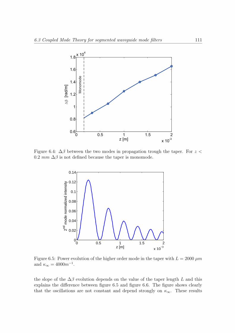
6.3 Coupled Mode Theory for segmented waveguide mode filters 111
0 0.5 1 1.5 2
x 10-3
0.6
0.8
1
1.2
1.4
1.6
1.8x 10
4
z [m]
Db
[ra
d/m
]
Mono
mode
Figure 6.4: ∆β between the two modes in propagation trough the taper. For z <0.2 mm ∆β is not defined because the taper is monomode.
0 0.5 1 1.5 2
x 10−3
0
0.02
0.04
0.06
0.08
0.1
0.12
0.14
z [m]
2nd m
ode
norm
aliz
ed in
tens
ity
Figure 6.5: Power evolution of the higher order mode in the taper with L = 2000 µmand κ∞ = 4000m−1.
the slope of the ∆β evolution depends on the value of the taper length L and thisexplains the difference between figure 6.5 and figure 6.6. The figure shows clearlythat the oscillations are not constant and depend strongly on κ∞. These results

112 6. Segmented waveguide mode filter
0 0.5 1 1.5 2
x 10−3
0
0.01
0.02
0.03
0.04
0.05
0.06
0.07
L [m]
2nd m
ode
norm
aliz
ed in
tens
ity
κ∞=5000m−1
κ∞ =4000m−1
κ∞=3000m−1
Figure 6.6: Power evolution of the higher order mode at the output of the taperas a function of the length L for κ∞ = 4000m−1 (continuous line), κ∞ = 5000m−1
(dashed line) and κ∞ = 3000m−1 (dotted line).
also suggest that even a relatively short taper, if correctly designed, can preventthe excitation of the higher order mode. To do so, one must simply choose L incorrespondence of an higher order mode minimum. However, this solution is criticalbecause of the difficulty to evaluate correctly κ∞. In many cases, it is then muchbetter to design a longer taper working with strongly attenuated oscillations. In thiscase, even if we don’t know exactly the κ∞ value, the higher order mode excitationresults small.
6.4 Experimental results
In order to confirm the working principle of a segmented waveguide mode filterwe have fabricated the devices sketched in figure 6.7. With respect the structure
WaveguidePSWInput TAPER Output TAPERWaveguide
Figure 6.7: Scheme of the fabricated mode filter. The segmented waveguide (SWG)is placed between two continuous waveguide with two tapers to optimize coupling.
proposed by Chou et al. [34], the segmented waveguide is between two continuous

6.4 Experimental results 113
DCm P [µm] W [µm] L [µm]0.3 - 0.4 - 0.5 10 - 15 - 25 5 - 7 100 - 600 - 1000 - 1600 - 2000
Table 6.2: Geometrical parameters of the taper.
waveguides and not at the edge of the sample. The input and output tapers areequal and the segmented waveguide is 5 mm long in order completely eliminatethe mode at cutoff. These devices have been fabricated with different characteristicparameters. The values of the period P , the duty cycle DCm and the taper lengthL combined to fabricate different structures are summarized in the following table6.2.
In the sample, we have also fabricated continuous and segmented waveguides(without tapers) in order to evidence respectively the multimodality and the filtereffect.
A schematic representation of the experimental setup adopted to characterizethe properties of our mode filters is shown in figure 6.8. The source is a diode laser,
V
Laser
840nmSample
Input
objective objective
Output
splitter
Beam
Detector
Hamamatsu camera
Piezocontroller
Figure 6.8: Experimental setup adopted to characterize the fabricated mode filters.
emitting at λ = 840 nm. The incident beam is end fire coupled to the samplewith an input microscope objective. The output signal is collected by an othermicroscope objective and then split by a semi-reflecting mirror. One beam is sentto an infrared camera (Hamamatsu) and the other one is sent to a detector for theevaluation of the transmitted power. The camera allows to visualize in real time ona monitor the shape of the near field and evaluate the possible presence of higherorder modes. The input microscope objective is mounted on a piezoelectric stage.This system controls accurately the position of the objective allowing to modify theexciting condition of the waveguides.
The characterization procedure determines the signal power at the output ofthe sample as a function of the input objective position and records, at the sametime, the camera images. Figure 6.9 shows the results we have obtained comparingthe transmitted power in the case of continuous waveguide and of waveguide withmode filter and input and output tapers with L = 600 µm. The exciting condition
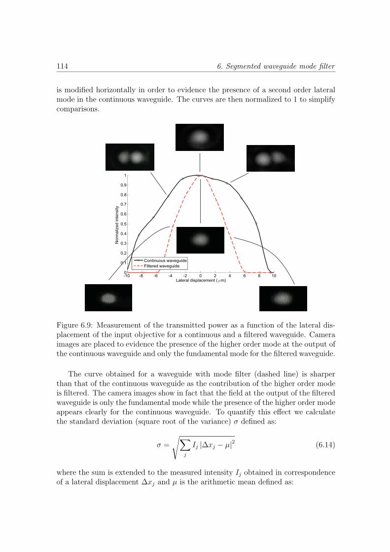
114 6. Segmented waveguide mode filter
is modified horizontally in order to evidence the presence of a second order lateralmode in the continuous waveguide. The curves are then normalized to 1 to simplifycomparisons.
-10 -8 -6 -4 -2 0 2 4 6 8 100
0.1
0.2
0.3
0.4
0.5
0.6
0.7
0.8
0.9
1
Lateral displacement ( m m)
Norm
aliz
ed inte
nsity
Continuous waveguide
Filtered waveguide
Figure 6.9: Measurement of the transmitted power as a function of the lateral dis-placement of the input objective for a continuous and a filtered waveguide. Cameraimages are placed to evidence the presence of the higher order mode at the output ofthe continuous waveguide and only the fundamental mode for the filtered waveguide.
The curve obtained for a waveguide with mode filter (dashed line) is sharperthan that of the continuous waveguide as the contribution of the higher order modeis filtered. The camera images show in fact that the field at the output of the filteredwaveguide is only the fundamental mode while the presence of the higher order modeappears clearly for the continuous waveguide. To quantify this effect we calculatethe standard deviation (square root of the variance) σ defined as:
σ =
√∑j
Ij |∆xj − µ|2 (6.14)
where the sum is extended to the measured intensity Ij obtained in correspondenceof a lateral displacement ∆xj and µ is the arithmetic mean defined as:

6.4 Experimental results 115
µ =
∑j
∆xjIj
∑j
Ij.(6.15)
We found that σ = 3.55µm for the waveguide with mode filter and σ = 8.2µm for thewaveguide without mode filter. We have then repeated the measurement for differentvalues of taper length L. In particular, when L = 2000 µm we have obtained theresults reported in figure 6.10. As expected for a taper of length L = 2000 µm the
-10 -8 -6 -4 -2 0 2 4 6 8 100
0.1
0.2
0.3
0.4
0.5
0.6
0.7
0.8
0.9
1
Lateral displacement ( m m)
No
rma
lize
d in
ten
sity
Continuous wavaguide
Filter: L=600mm
Filter: L=2000mm
Figure 6.10: Measurement of the transmitted power as a function of the lateraldisplacement of the input objective for a continuous and two filtered waveguideswith taper length L = 600 µm (dashed line) and L = 2000 µm (dotted line).The camera images confirm the monomodality of the filtered waveguide also forL = 2000 µm.
output field presents only the fundamental mode. However, rather surprisingly, thewidth of the transmission curve as a function of the lateral displacement is largerthan in the case of a taper with L = 600 µm. For L = 2000 µm, in fact, the valueof σ become 5.79 µm. The surprising result is that σ increases despite we wouldhave expected a decrease as larger taper are expected to provide better filteringconditions.
A possible explanation can come from the role played by the input taper. Thistaper are expected to convert efficiently the energy of the fundamental mode of the
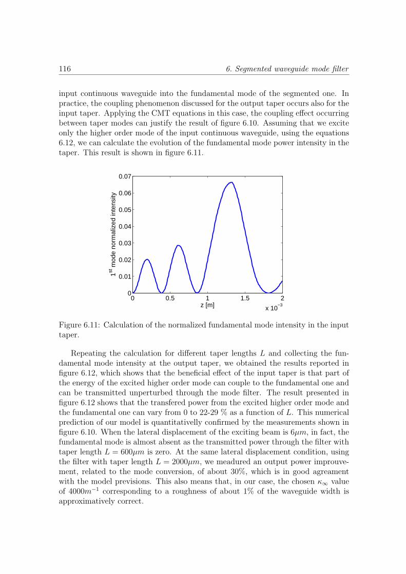
116 6. Segmented waveguide mode filter
input continuous waveguide into the fundamental mode of the segmented one. Inpractice, the coupling phenomenon discussed for the output taper occurs also for theinput taper. Applying the CMT equations in this case, the coupling effect occurringbetween taper modes can justify the result of figure 6.10. Assuming that we exciteonly the higher order mode of the input continuous waveguide, using the equations6.12, we can calculate the evolution of the fundamental mode power intensity in thetaper. This result is shown in figure 6.11.
0 0.5 1 1.5 2
x 10−3
0
0.01
0.02
0.03
0.04
0.05
0.06
0.07
z [m]
1st m
ode
norm
aliz
ed in
tens
ity
Figure 6.11: Calculation of the normalized fundamental mode intensity in the inputtaper.
Repeating the calculation for different taper lengths L and collecting the fun-damental mode intensity at the output taper, we obtained the results reported infigure 6.12, which shows that the beneficial effect of the input taper is that part ofthe energy of the excited higher order mode can couple to the fundamental one andcan be transmitted unperturbed through the mode filter. The result presented infigure 6.12 shows that the transfered power from the excited higher order mode andthe fundamental one can vary from 0 to 22-29 % as a function of L. This numericalprediction of our model is quantitativelly confirmed by the measurements shown infigure 6.10. When the lateral displacement of the exciting beam is 6µm, in fact, thefundamental mode is almost absent as the transmitted power through the filter withtaper length L = 600µm is zero. At the same lateral displacement condition, usingthe filter with taper length L = 2000µm, we meadured an output power improuve-ment, related to the mode conversion, of about 30%, which is in good agreamentwith the model previsions. This also means that, in our case, the chosen κ∞ valueof 4000m−1 corresponding to a roughness of about 1% of the waveguide width isapproximatively correct.
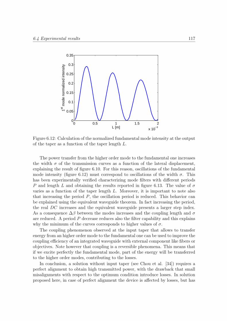
6.4 Experimental results 117
0 0.5 1 1.5 2
x 10−3
0
0.05
0.1
0.15
0.2
0.25
0.3
0.35
L [m]
1st m
ode
norm
aliz
ed in
tens
ity
Figure 6.12: Calculation of the normalized fundamental mode intensity at the outputof the taper as a function of the taper length L.
The power transfer from the higher order mode to the fundamental one increasesthe width σ of the transmission curves as a function of the lateral displacement,explaining the result of figure 6.10. For this reason, oscillations of the fundamentalmode intensity (figure 6.12) must correspond to oscillations of the width σ. Thishas been experimentally verified characterizing mode filters with different periodsP and length L and obtaining the results reported in figure 6.13. The value of σvaries as a function of the taper length L. Moreover, it is important to note alsothat increasing the period P , the oscillation period is reduced. This behavior canbe explained using the equivalent waveguide theorem. In fact increasing the period,the real DC increases and the equivalent waveguide presents a larger step index.As a consequence ∆β between the modes increases and the coupling length and σare reduced. A period P decrease reduces also the filter capability and this explainswhy the minimum of the curves corresponds to higher values of σ.
The coupling phenomenon observed at the input taper that allows to transferenergy from an higher order mode to the fundamental one can be used to improve thecoupling efficiency of an integrated waveguide with external component like fibers orobjectives. Note however that coupling is a reversible phenomena. This means thatif we excite perfectly the fundamental mode, part of the energy will be transferredto the higher order modes, contributing to the losses.
In conclusion, a solution without input taper (see Chou et al. [34]) requires aperfect alignment to obtain high transmitted power, with the drawback that smallmisalignments with respect to the optimum condition introduce losses. In solutionproposed here, in case of perfect alignment the device is affected by losses, but has

118 6. Segmented waveguide mode filter
0 500 1000 1500 20000
2
4
6
8
10
L [mm]
Sta
ndard
devia
tion
s [
mm
]
Continuous waveguide
filter: P=10mmfilter: P=15mm
filter: P=25mm
Figure 6.13: Measurement of the width σ as a function of the taper length L fordifferent period P . The red line corresponds to the reference width σ obtained inthe case of multimode continuous waveguide.
better coupling tolerances with external devices. This is important in case of fiberoptics pigtailing where the cost of the system is related to the desired alignmentprecision.
The drawback of this structure is that device behavior is strongly dependenton the coupling coefficient κ, which depends on technological imperfections. As aconsequence, the design of the structure may be very difficult and the results notreproducible. To overcome this problem we propose a new structure that can beobtained introducing a purpose surface roughness (figure 6.14).The periodicity of the lateral profile of the input taper can be used to obtain the
TaperContinuouswaveguide
Segmentedwaveguide
Figure 6.14: Schematic of mode filter with controlled artificial irregularity at theinput taper.
phase matching condition between the modes we want to couple. In this case, propa-gation losses would not be increased because the matching condition will be betweenpropagating mode instead of radiating modes. Note also that being ∆β variable in

6.4 Experimental results 119
the taper also the periodicity of the lateral profile must change longitudinally.

120 6. Segmented waveguide mode filter

Conclusions
In this thesis, we have reported the main results achieved during my work con-cerning new devices for photonics applications. The research has been developedfollowing all the steps which lead to the realization of a device prototype in inte-grated optics: its design, developing and using suitable numerical tools, the choiceof the substrate material in which the device is fabricated and the relevant tech-nology, and its characterization, with a suitable experimental setup. Following allthese steps allowed me to merge the interest for physical insight into the basics ofdevice behavior, which animates the doctorate “Specialite Physique” of the Univer-sity of Nice-Sophia Antipolis, and the engineering oriented search of feasible andcost effective components, underlying the activities of the doctorate in “IngegneriaElettronica, Informatica e delle Telecomunicazioni” of the University of Bologna.This is in fact a co-tutored PhD made possible by the “Unversita Italo-Francese”,who provided a fellowship in the framework of the Vinci Program.
The problem to tackle and hopefully to solve concerned possible devices able toreduce losses when connecting waveguides of different shape and/or materials. Thisis still a challenging issue in optical telecommunication systems, either to reducecoupling losses, or to allow less critical, and then less expensive, coupling betweendifferent devices.
Physics of periodic, or almost periodic, structures has been chosen as basic prin-ciple for device operation as it seemed that properties of these waveguides fitted wellboth simplicity and possibility of tailoring device functionality. So, after studyingtheir main characteristics of light propagation in these structures, an investigationon their many applications in optics has been done, evidencing their possible appli-cations to our purposes.
The characteristics of these structures prevent the use of analytical approaches,except that for preliminary or simplified analysis. So some numerical tools have beendeveloped, aiming at studying propagation in these structures. In particular, a FiniteDifference 3D-Beam Propagation Method (3D-BPM), based on the electric fieldformulation of the Helmholtz equations, previously developed in the Italian group,has been improved and adapted for the study of segmented waveguide structures.Moreover, we have completely developed a second version of this tool, based on themagnetic field formulation, to solve some numerical instability problems intrinsic ofthe previous version. In both cases we have implemented Perfect Matched Layer
122 Conclusions
(PML) boundary conditions and Pade approximants for wild angle propagationanalysis. In parallel to this, we have also developed a mode solver, able to studylongitudinally invariant structures, such as optical fibers and continuous waveguides.This tool can also be used to determine the input field necessary to run BPMsimulations.
A second step to do was the choice of the material and the technology to beused for waveguide fabrication. Lithium Niobate substrate and Soft Proton Ex-change (SPE) technology have been chosen. Lithium Niobate is in fact one of thefavorite materials in integrated optics because of its very good linear and nonlinearproperties. The SPE technique is routinely used in the French laboratory wherethe experimental part of the work has been developed. Using this technique andusing CAD assisted design, we have then fabricated segmented waveguide tapersand mode filters. This part required a merge of the two different expertises. Infact numerical modelling of waveguides depends strongly on the used material andfabrication technology, also to include a realistic model of the structure. This al-lowed, for example, to identify in the roughness of the sample’s surface a fabricationproblem to be considered to improve the present fabrication technology.
Once waveguides have been fabricated, they have also to be characterized. Wehave then identified the main parameters to be measured (propagation losses, effec-tive group index and mode size) and set up an apparatus to measure them. Thesystem is controlled by a computer with a Labview program which allows to performautomatic measurements. Precautions have been adopted to avoid systematic errors(spurious cavities between sample and fibers, mechanical changes due to operatorinduced temperature variations, etc.). Possible ways for further improvement ofprecision and accuracy of the setup have been identified: lasers with stable internalor external polarization control to guarantee good polarization stability for widewavelength ranges, positioning control of the piezoelectric adjuster with capacitiveprobes to increase spatial scanning resolution up to nanometric precision and toeliminate the hysteresis problems and the temporal drift.
The versatility and the possibilities offered by the proposed setup have beenconfirmed by the results of measurements performed on various samples, either in-tegrated optical waveguides or optical fibers. Using this setup we have characterizedsegmented waveguide tapers fabricated in LiNbO3 by the SPE process. Experimen-tal results have been obtained at telecom wavelengths. We have found that whenone uses the SPE parameters necessary to reach the maximum confinement of theguided mode, preserving non-linear and electro-optical coefficients, the introductionof an adapted taper allows reducing by 0.78 dB the coupling losses with a standardSMF-28 fiber. For a complete device, presenting optimized tapers at input and out-put, the benefit could then reach 1.5 dB. All the experimental results are in goodagreement with the numerical analysis confirming the precision of the developednumerical tools and the quality of the model. This structure has been introduced ina more complicated structure, a quantum relay developed at LPMC by Guillaume

123
Bertocchi to be used in quantum transmission experiments, obtaining the expectedimprovement in terms of insertion losses.
We have also designed, realized and characterized a segmented waveguide actingas a mode filter operating at λ = 840 nm. A new structure has been proposed and asemi-analytical formulation, based on the Coupled Mode Theory, has been used todesign the filter parameters. The measurement setup able to characterize this deviceuses a camera to acquire the near field at the output of the sample, evaluating thepresence of higher order modes, while the position of the input microscope objective,used to launch the light in the waveguide, is modified through a piezoelectric system.The output power is also measured as a function of the exciting condition in orderto evaluate the coupling sensibility. Experimentally, the second higher order modehas been successfully eliminated from a multimode continuous waveguide. Duringthe characterization procedure we have obtained interesting result on the outputpower measurements as a function of the objective position. We have proposed anexplanation, considering the mode coupling at the entrance of the filter, obtainingagreements with experimental results.
These devices should hopefully be useful to improve coupling between fibers andintegrated optical devices allowing both mode mismatch and alignment tolerancereduction. The mode filter has also interesting applications in non linear opticsexperiments, eliminating higher order pump modes as their presence can perturbthe non linear process efficiency and the output spectrum by generating undesiredwavelengths.

124 Conclusions

Author’s references
• R. Zoli, M. Gnan, D. Castaldini, G. Bellanca, and P. Bassi, “Reformulationof the plane wave method to model photonic crystal”, OSA Optics Express,November 3, vol. 11, p. 2905-2910, 2003.
• R. Zoli, D. Castaldini, M. Gnan, G. Bellanca, and P. Bassi, “2d and 3d numer-ical investigation of photonic crystal waveguides”, Proceedings of NUMELEC,2003.
• D. Castaldini, R. Zoli, A. Parini, G. Bellanca, and P. Bassi, “2d or 3d fdtd forphotonic crystal waveguides modeling?”, Proceedings of PIERS 2004, Progressin Electromagnetics Research Symposium, 28-31 March 2004, Pisa, Italy, pp.381-384.
• D. Castaldini, “Analisi accurata di guide a cristallo fotonico 3d,” Atti della XVRiNEm, Riunione Nazionale di Elettromagnetismo, Cagliari, 13-16 Settembre2004.
• G. Bertocchi, D. Castaldini, S. Tascu, D. B. Ostrowsky, S. Tanzilli, M. De Micheli,and P. Baldi, “Integrated-optics quantum relay : Preliminary results”, Pro-ceedings of the 32nd European Conference on Optical Communication (ECOC),Cannes, 24th-28th September 2006, vol 6, Paper We3.P.200, pp.91-92.
• D. Castaldini, P. Bassi, S. Tascu, S. Gregory, P. Aschieri, M. De Micheli,P. Baldi, K. Thyagarajan, and M. R. Shenoyc, “All-in-one measurement setupfor fast and accurate characterization of linear guided-wave optical devices”,submitted to Optical Engineering.
• D. Castaldini, P. Bassi, S. Tascu, P. Aschieri, M. De Micheli, and P. Baldi,“Soft proton exchange tapers for low insertion loss LiNbO3 devices”, acceptedfor publication in the IEEE/OSA Journal of Lightwave Technology.
• D. Castaldini, P. Bassi, G. Bertocchi, S. Tascu, P. Aschieri, M. De Micheli,S. Tanzilli and P. Baldi “Segmented waveguide tapers for low insertion loss,high performance SPE:LiNbO3 integrated circuits”, accepted for 13th Euro-pean Conference on Integrated Optics (ECIO), 25-27 April 2007.

126 Author’s references
Bibliography
[1] G. P. Agrawal, Fiber-optic communication systems, 3rd, Ed. J. Wiley & Sons,2002.
[2] D. Hussein, T. Mouftah, and J. Zheng, Optical WDM Networks: Concepts anddesign principles. Wiley-IEEE, 2004.
[3] R. W. Boyd, Nonlinear Optics. Elsevier, 2003.
[4] H. Herrmann and W. Sohler, “Difference-frequency generation of tunable, co-herent mid-infrared radiation in Ti : LiNbO3 channel waveguides,” J. Opt.Soc. Am. B, vol. 5, p. 278, 1988.
[5] C. H. Bennett and D. P. D. Vincenzo, “Quantum information and computa-tion,” Nature, vol. 404, pp. 247–255, 2000.
[6] D. Bouwmeester, A. K. Ekert, and A. Zeilinger, The Physics of Quantum In-formation: Quantum Cryptography, Quantum Teleportation, Quantum Com-putation. Springer Verlag, 2000.
[7] K. Sakoda, Optical properties of photonic crystals. Springer, 2001.
[8] D. D. Stancil, “Kronig-penney model for periodically segmented waveguides,”Applied Optics, vol. 35, p. 4767, 1996.
[9] A. Yariv and P. Yeh, Optical Waves in Crystals. J. Wiley & Sons, 1984.
[10] R. E. Collin, “Reflection and transmission at a slotted dielectric interface,”Can.J.Phys, vol. 34, p. 398, 1956.
[11] L. R. Lewis and A. Hessel, “Propagation characteristics of periodic arrays ofdielectric slabs,” IEEE Transactions on Microwave Theory and Techniques,vol. MTT-19, p. 276, 1971.
[12] K. Thyagarajan, C. W. Chien, R. V. Ramaswamy, H. S. Kim, and H. C.Cheng, “Proton-exchanged periodically segmented waveguides in LiNbO3,”Optics Letters, vol. 19, p. 880, 1994.

128 Bibliography
[13] K. Thyagarajan, V. Mahalakshmi, and M. R. Shenoy, “Propagation character-istics of planar segmented waveguides with parabolic index segments,” OpticsLetters, vol. 19, p. 2113, 1994.
[14] F. Fogli, N. Greco, P. Bassi, G. Bellanca, P. Aschieri, and P. Baldi, “Spatialharmonics modeling of planar periodic segmented waveguide,” Optical andQuantum Electronics, vol. 33, no. 4-5, pp. 485–498, 2001.
[15] F. Fogli, G. Bellanca, P. Aschieri, M. De Micheli, and P. Bassi, “Spatial har-monics analysis of deep waveguide bragg gratings,” Opt. A, vol. 6, pp. 433–438,2004.
[16] L. Li and J. J. Burke, “Linear propagation characteristics of periodically seg-mented waveguides,” Optics Letters, vol. 17, no. 17, pp. 1195–1197, September1992.
[17] J. D. Bierlein, “Propagation in segmented waveguide structures,” QuantumElectronics and Laser Science, vol. 13, p. 42, 1992.
[18] V. Rastogi, V. Mahalakshmi, M. R. Shenoy, and K. Thyagarajan, “Propa-gation characteristics of a novel complementary-structure planar segmentedwaveguide,” Optics Communications, vol. 148, pp. 230–235, 1998.
[19] D. Ortega, R. M. De La Rue, and J. S. Aitchison, “Cutoff wavelength of peri-odically segmented waveguides in Ti : LiNbO3,” IEEE Journal Of LightwaveTechnology, vol. 16, pp. 284–291, 1998.
[20] G. B. Hocker and W. Burns, “Modes in diffused optical waveguides of arbitraryindex profile,” IEEE Journal of Quantum Electronics, vol. QE-11, pp. 270–276, 1975.
[21] A. W. Snyder and R. M. De La Rue, “Asymptotic solution of eigenvalueequations for surface waveguide structures,” IEEE Transactions MicrowaveTheory Tech., vol. MTT-18, p. 650, 1970.
[22] H. Kogelnik and W. Burns, “Scaling rules for thin-film optical waveguides,”Applied Optics, vol. 13, pp. 1857–1862, 1974.
[23] G. B. Hocker and W. Burns, “Mode dispersion in diffused chanel waveguidesby the effective index method,” Applied Optics, vol. 16, pp. 113–118, 1977.
[24] S. G. Johnson, P. Bienstman, M. A. Skorobogatiy, M. Ibanescu, E. Lidorikis,and J. D. Joannopoulos, “Adiabatic theorem and continuous coupled-modetheory for efficient taper transition in photonic crystal,” Phisical Review,vol. 66, pp. 1–15, 2002.

Bibliography 129
[25] R. Kashyap, Fiber Bragg Gratings. Academic Press, 1999.
[26] M. L. Povinelli, S. G. Johnson, and J. D. Joannopoulos, “Slow-light, band-edgewaveguides for tunable time delays,” Nature, vol. 438, p. 65, 2005.
[27] R. de Ridder, R. Wijbrans, H. Albers, J. Aukema, P. Lambeck, J. Hoekstra,and A. Driessen, “A spot-size transformer for fiber-chip coupling in sensorapplications at 633 nm in silicon oxynitride,” in Lasers and Electro-OpticsSociety Annual Meeting, 1995. 8th Annual Meeting Conference Proceedings,Volume 1., IEEE, vol. 2, 30-31 Oct. 1995, pp. 86–87vol.2.
[28] Z. Weissman, “Evanescent field sensors with periodically segmented wave-guides,” Applied Optics, vol. 36, p. 1218, 1997.
[29] J. V. Lith, P. Lambeck, H. Hoekstra, R. Heideman, and R. Wijn, “The seg-mented waveguide sensor: principle and experiments,” IEEE Journal of Light-wave Technology, vol. 23, no. 1, pp. 355–363, Jan. 2005.
[30] A. B. Aceves, “Optical gap solitons: Past, present, and future: theory andexperiments,” CHAOS, vol. 10, pp. 584–589, 2000.
[31] S. Trillo and W. Torruellas, Spatial solitons. Springer, 2001.
[32] P. Baldi, M. R. Shenoy, S. Nouh, M. De Micheli, and D. B. Ostrowsky, “Esti-mation of the extent and influence of longitudinal diffusion on LiNbO3 protonexchanged segmented stripe waveguides,” Optics Communications, vol. 104,pp. 308–312, 1994.
[33] Z. Weissman and A. Hardy, “2-d mode tapering via tapered channel waveguidesegmentation,” Electronics letters, vol. 28, p. 1514, 1992.
[34] M. H. Chou, M. A. Arbore, and M. M. Fejer, “Adiabatically tapered peri-odic segmentation of channel waveguides for mode size transformation andfundamental mode excitation,” Optics Letters, vol. 21, pp. 794–796, 1996.
[35] F. Fogli, G. Bellanca, P. Bassi, I. Madden, and W. Johnstone, “Highly efficientfull-vectorial 3-D BPM modeling of fiber to planar waveguide couplers,” IEEEJournal of Lightwave Technology, vol. 17, no. 1, pp. 136–143, Jan. 1999.
[36] F. Fogli, G. Bellanca, and P.Bassi, “Tbc and pml conditions for 2d and 3dbpm : a comparison,” Optical and quantum electronics, vol. 30, pp. 443–456,1998.
[37] J. A. Stratton, Electromagnetic theory. Mc Graw Hill, 1941.
[38] P. Bassi, G. Bellanca, and G. Tartarini, Propagazione ottica libera e guidata.Clueb, 1999.
130 Bibliography
[39] D. Yevick, “The application of complex pade approximants to vector fieldpropagation,” IEEE Photon. Technol. Lett., vol. 12, no. 12, pp. 1636–1638,2000.
[40] G. R. Hadley, “Wide-angle beam propagation using pade approximant opera-tors,” Optics Letters, vol. 17, pp. 1426–1428, 1992.
[41] K. Saitoh and M. Koshiba, “Approximate scalar finite-element beam-propagation method with perfectly matched layers for anisotropic opticalwaveguides,” J. Light-wave Technol., vol. 19, no. 5, pp. 786–792, 2001.
[42] G. D. Smith, Numerical Solution of partial differential equations: finite differ-ence methods. Oxford University Press, 1985.
[43] D. Li, “The fully vectorial beam propagation method,” Ph.D. dissertation,Delft, 1995.
[44] C. L. Xu, W. P. Huang, S. K. Chaudhuri, and J. Chrostowski, “An uncondi-tionally stable vectorial beam propagation method for 3-d structures,” IEEEPhoton.Technol. Lett., vol. 6, no. 4, pp. 549–551, 1994.
[45] C. L. Xu and W. P. Huang, “Finite-difference beam-propagation method forguide-wave optics,” in Progress In Electromagnetic Waves: PIERS 11, Cam-bridge, 1995.
[46] J. L. Volakis, A. Chatterjee, and L. C. Kempel, Finite Element Method forElectromagnetics: Antennas, Microwave Circuits, and Scattering Applications.IEEE Press, 1998.
[47] Y. Saad, Iterative methods for sparse linear systems. 2nd ed. Philadelphia:Society for Industrial and Applied Mathematics (SIAM), 2003.
[48] G. R. Hadley, “Transparent boundary condition for beam propagation,” OpticsLetters, vol. 16, no. 9, pp. 624–626, 1991.
[49] J.-P. Berenger, “A perfectly matched layer for the absorbtion of electromag-netic waves,” Journal of Computational Physics, vol. 114, pp. 185–200, 1994.
[50] Z. Sacks, D. Kingsland, R. Lee, and J.-F. Lee, “A perfectly matchedanisotropic absorber for use as an absorbing boundary condition,” Antennasand Propagation, IEEE Transactions on, vol. 43, no. 12, pp. 1460–1463, Dec.1995.
[51] A. Cucinotta, G. Pelosi, S. Selleri, L. Vincetti, and M. Zoboli, “Perfectlymatched anisotropic layers for optical waveguides analysis through the finiteelement beam propagation method,” Microwave and Optical Technology Let-ters, vol. 23, no. 2, pp. 67–69, 1999.

Bibliography 131
[52] W. P. Huang, C. L. Xu, W. Lui, and K. Yokoyama, “The perfectly matchedlayer (pml) boundary condition for the beam propagation method,” IEEEPhoton. Technol. Lett., vol. 8, no. 5, pp. 649–651, 1996.
[53] M. Hikari, M. Koshiba, and Y. Tsuji, “A time domain beam propagationmethod based on a finite element scheme,” Electronics and Communicationsin Japan, vol. 82, pp. 52–58, 1999.
[54] C. Vassallo, “Wide-angle bpm and power conservation,” IEE Electron. Lett.,vol. 31, pp. 130–131, 1995.
[55] P. Lusse, P. Stuwe, J. Schule, and H. G. Unger, “Analysis of vetorial modefields in optical waveguide by a new finite difference method,” IEEE Journalof Lightwave Technology, vol. 12, no. 3, pp. 487–494, 1994.
[56] M. J. Robertson, S. Ritchie, and P. Dayan, “Semiconductor waveguides: anali-ysis of optical propagation in single rib structures and directional couplers,”Proc. Inst. Elec. Eng., vol. 132, pp. 336–342, 1985.
[57] A. Delage, “Modelling of semiconductor rib waveguides by a finite differencemethod,” Can. J. Phys., vol. 69, pp. 512–519, 1991.
[58] A. Vassallo, “Improved finite difference deviation of semi-vectorial modes in3d step index waveguides,” in European conference on optical communications,Berlin, 1991.
[59] M. S. Stern, “Semivectorial polarised finite difference methods for opticalwaveguides with arbitrary index profiles,” Proc. Inst. Elec. Eng., vol. 135,pp. 56–63, 1988.
[60] M. Fujimura and T. Suhara, Waveguide Nonlinear Optic Devices. Springer,2003.
[61] J. R. Carruthers, I. P. Kaminow, and L. W. Stulz, “Diffusion kinetics andoptical waveguiding properties of outdiffused layers in lithium niobate andlithium tantalite,” App. Opt., vol. 13, pp. 2333–2342, 1974.
[62] G. J. Griffiths and R. J. Esdaile, “Analysis of titanium diffused planar opticalwaveguides in lithium niobate,” IEEE Journal of Quantum Electronics, vol. 20,pp. 149–159, 1984.
[63] M. L. Shah, “Optical waveguides in LiNbO3 by ion exchange technique,” App.Phys. Lett, vol. 26, pp. 652–653, 1975.
[64] J. L. Jackel, C. E. Rice, and J. J. Veselka, “Proton exchange for high-indexwaveguides in LiNbO3,” App. Phys. Lett, vol. 41, pp. 607–608, 1982.

132 Bibliography
[65] M. L. Bortz and M. M. Fejer, “Annealed proton-exchanged LiNbO3 wave-guides,” Opt. Lett., vol. 16, pp. 1844–1846, 1991.
[66] L. Chanvillard, P. Aschieri, P. Baldi, D. B. Ostrowsky, M. De Micheli,L.Huang, and D. J. Bamford, “Soft proton exchange on PPLN: a simple wave-guide fabrication process for highly efficient non-linear interactions,” Appl.Phys. Lett., vol. 76, pp. 1089–1091, 2000.
[67] Y. N. Korkishko and V. A. Fedorov, “Structural phase diagram ofHxLi1−xNbO3 waveguides: the correlation between optical and structuralproperties,” IEEE Journal of Selected Topics in Quantum Electronics, vol. 2,pp. 187–196, 1996.
[68] C. Canali, A. Carnera, G. della Mea, P. Mazzoldi, S. M. A. Shukri, A. C. G.Nutt, and R. M. De La Rue, “Structural characterization of proton exchangedLiNbO3 optical waveguides,” J. Appl. Phys, vol. 59, pp. 2643–2649, 1986.
[69] Y. N. Korkishko, V. A. Fedorov, E. A. Baranov, M. V. Proyaeva, T. V. Moro-zova, F. Caccavale, F. Segato, C. Sada, and S. M. Kostritskii, “Characteriza-tion of alpha-phase soft proton-exchanged LiNbO3 optical waveguides,” JOSAA, vol. 18, pp. 1186–1191, 2001.
[70] K. E. Hadi, V. Rastogi, M. R. Shenoy, K. Thyagarajan, M. De Micheli, andD. B. Ostrowsky, “Spectral measurement of the film substrate index differencein proton-exchanged LiNbO3 waveguides,” Applied Optics, vol. 37, pp. 6463–6467, 1998.
[71] P. Aumont, “Realisation par echange protonique doux de guides continueset segmentes sur niobate de lithium,” Ph.D. dissertation, Laboratoire dePhysique de la Matiere Condensee, 2003.
[72] [Online]. Available: www.barnardmicrosystems.com
[73] [Online]. Available: www.photronics.com
[74] P. Aschieri, V. Rastogi, L. Chanvillard, P. Baldi, M. De Micheli, D. B. Os-trowsky, G. Bellanca, P. Bassi, K. Thyagarajan, and M. R. Shenoy, “Exper-imental observation of longitudinal modulation of mode fields in periodicallysegmented waveguides,” Applied Optics, vol. 38, pp. 5734–5737, 1999.
[75] S. Monneret, P. H. Chantome, and F. Flory, “m-lines technique : prism cou-pling measurement and discussion of accuracy for homogeneous waveguides,”J. Opt. A: Pure Appl. Opt., vol. 2, pp. 188–195, 2000.

Bibliography 133
[76] P. Mathey, P. Jullien, , and J. L. Bolzinger, “Refractive - index profile recon-structions in planar waveguides by the WKB inverse method and reflectivitycalculations,” J. Opt. Soc. Am. B., vol. 12, pp. 1663–1670, 1995.
[77] L. P. Shi, E. Y. B. Pun, and P. S. Chung, “Extended iwkb method for deter-mination of the refractive index profile in optical waveguides,” Optics Letters,vol. 20, no. 15, pp. 1622–1624, 1995.
[78] D. Taillaert, W. Bogaerts, P. Bienstman, T. F. Krauss, P. V. Daele, I. Mo-erman, S. Verstuyft, K. D. Mesel, and R. Baets, “An out-of-plane gratingcoupler for efficient butt - coupling between compact planar waveguides andsingle - mode fibers,” IEEE Journal Of Quantum Electronics, vol. 38, no. 7,pp. 949–955, 2002.
[79] D. Castaldini, P. Bassi, S. Tascu, S. Gregory, P. Aschieri, M. De Micheli,P. Baldi, K. Thyagarajan, and M. R. Shenoyc, “All-in-one measurement setupfor fast and accurate characterization of linear guided-wave optical devices,”submitted to Opt. Eng.
[80] G. Tittelbach, B. Richeter, and W. Karthe, “Comparison of three transmis-sion methods for integrated optical waveguide propagation loss measurement,”Pure Appl. Opt., vol. 2, pp. 683–700, 1993.
[81] P. J. Brannon, “Improved method of measuring optical waveguide propagationlosses,” Applied Optics, vol. 25, no. 20, pp. 3596–3598, 1986.
[82] D. B. Ostrowsky, A. M. Roy, and J. Sevin, “Integrated optical waveguideexamination using anti-stokes fluorescence,” Applied Physics Letter, vol. 24,pp. 553–554, 1974.
[83] R. Regener and W. Sohler, “Loss in low-finesse Ti : LiNbO3 optical waveguideresonators,” Applied Physics B, vol. 36, pp. 143–147, 1985.
[84] A. Ghatak and k. Thyagarajan, An Introduction to Fiber Optics. CambridgeUniversity Press, 1998.
[85] L. G. Cohen and C. Lin, “A universal fiber-optic (UFO) measurement systembased on a near-ir raman laser,” IEEE J. Quantum Electron., vol. QE-14, pp.855–859, 1978.
[86] C. Lin, A. R. Tynes, A. Tomita, P. L. Lin, and D. L. Philen, “Chromaticdispersion measurements in single-mode fibers using picosecond InGaAsP in-jection lasers in the 1.2 to 1.5 pm spectral region,” Bell Syst. Tech. J ., vol. 62,no. 2, pp. 457–462, 1983.

134 Bibliography
[87] M. J. Saunders and W. B. Gardner, “Precision interferometric measurementof dispersion in short single mode fibers,” in Tech Dig. NBS Symp. on Opt.Fib. Meas. (Boulder, CO), Oct. 2-3, 123-126, 1984.
[88] H. T. Shang, “Chromatic dispersion measurement by white-light interferom-etry on metre-length single-mode optical fibers,” Electron. Lett., vol. 17, pp.603–605, 1981.
[89] R. Zoli, M. Gnan, D. Castaldini, G. Bellanca, and P. Bassi, “Reformulationof the plane wave method to model photonic crystal,” Opt. Express, vol. 11,p. 2905, 2003.
[90] R. Zoli, D. Castaldini, M. Gnan, G. Bellanca, and P. Bassi, “2d and 3d nu-merical investigation of photonic crystal waveguides,” in NUMELEC, 2003.
[91] D. Castaldini, R. Zoli, A. Parini, G. Bellanca, and P. Bassi, “2d or 3d fdtdmodeling of photonic crystal waveguides?” in PIERS, 2003.
[92] D. Castaldini, “Analisi accurata di guide a cristallo fotonico 3d,” in RINEM,2004.
[93] Y. A. Vlasov, M. O’Boyle, H. F. Hamann, and S. J. McNab, “Active control ofslow light on chip with photonic crystal waveguides,” Nature, vol. 438, p. 65,2005.
[94] A. Melloni, F. Morichetti, and M. Martinelli, “Optical slow-wave structures,”in Prof. of 31st European Conference on Optical Communication, Glasgow,UK, 25-29 Sept., 2005.
[95] J. P. Pocholle, J. Auge, and M. Papuchon, “Determination of modal disper-sion in monomode fibres from wavelength dependence of the mode spot size,”Electron. Lett., vol. 19, no. 25/26, pp. 1093–1094, 1983.
[96] C. D. Hussey, “Field to dispersion relationships in single-mode fibers,” Elec-tron. Lett., vol. 20, no. 25/26, pp. 1251–1252, 1984.
[97] M. Notomi, K. Yamada, A. Shinya, J. Takahashi, C. Takahashi, and I. Yoko-hama, “Extremely large group-velocity dispersion of line-defect waveguidesin photonic crystal slabs,” Physical Review Letters, vol. 87, pp. 253 902–1–253 902–4, 2001.
[98] F. Alard, L. Jeunehomme, and P. Sansonetti, “Fundamental mode spot-sizemeasurement in single-mode optical fibers,” Electron. Lett., vol. 17, pp. 958–960, 1981.

Bibliography 135
[99] D. Hannappe and J. Desbois, “Original method for measurement of opticalmode fields,” Applied Optics, vol. 35, no. 4, pp. 659–662, 1996.
[100] A. T. Klemas, W. A. Reed, D. S. Shenk, and M. A. Saifi, “Analysis of mode-field radius calculated from far-field radiation patterns,” in Tech. Dig. OFS85(San Diego, CA), Feb. 11-13, 30-31, 1985.
[101] [Online]. Available: http://www.ni.com/labview/
[102] D. Marcuse, Light Transmission Optics, 2nd Ed. Van Nostrand, 1982.
[103] K. Petermann, “Constraints for fundamental-mode spot size broad-banddispersion-compensated single-mode fibers,” Electron. Lett., vol. 19, p. 712,1983.
[104] Corning SMF28 Optical Fiber Product Information, PI1036, (2002).
[105] R. Alferness, V. Ramaswamy, S. Korotky, M. Divino, and L. Buhl, “Effi-cient single-mode fiber to titanium diffused lithium niobate waveguide cou-pling forλ = 1.32µm,” IEEE Journal of Quantum Electronics, vol. 18, no. 10,pp. 1807–1813, Oct 1982.
[106] P. Suchoski and R. Ramaswamy, “Constant-width variable-index transition forefficient Ti : LiNbO3 waveguide-fiber coupling,” IEEE Journal Of LightwaveTechnology, vol. 5, pp. 1246–1251, 1987.
[107] K. Kasaya, O. Mitomi, M. Naganuma, Y. Kondo, and Y. Noguchi, “A simplelaterally tapered waveguide for low-loss coupling to single-mode fibers,” IEEEJournal of Photonics Technology Letters, vol. 5, no. 3, pp. 345–347, March1993.
[108] B. Luyssaert, P. Bienstman, P. Vandersteegen, P. Dumon, and R. Baets, “Ef-ficient nonadiabatic planar waveguide tapers,” IEEE Journal Of LightwaveTechnology, vol. 23, pp. 2462–2468, 2005.
[109] F. Dorgeuille, B. Mersali, S. Francois, G. Herve-Gruyer, and M. Filoche, “Spotsize transformer with a periodically segmented waveguide based on InP,” Op-tics Letters, vol. 20, pp. 581–583, 1995.
[110] M. M. Spuhler, B. J. Offrein, G.-L. Bona, R. Germann, I. Massarek, andD. Erni, “A very short planar silica spot-size converter using a nonperiodicsegmented waveguide,” IEEE Journal Of Lightwave Technology, vol. 16, p.1680, 1998.
[111] Z. Weissman and I. Hendel, “Analysis of periodically segmented waveguidemode expanders,” IEEE Journal Of Lightwave Technology, vol. 13, pp. 2053–2058, 1995.
136 Bibliography
[112] M. Yanagisawa, Y. Yamada, and M. Kobayashi, “Low-loss and large tolerancefiber coupling of high-∆ silica waveguides by local mode-field conversion,”IEEE Photonics Technology Letters, vol. 4, pp. 433–435, 1993.
[113] O. Alibart, S. Tanzilli, D. B. Ostrowsky, and P. Baldi, “Guided wave tech-nology for telecom wavelength heralded single photon source,” Optics Letters,vol. 30, pp. 1539–1541, 2005.
[114] D. Castaldini, P. Bassi, S. Tascu, P. Aschieri, M. De Micheli, and P. Baldi,“Soft proton exchange tapers for low insertion loss LiNbO3 devices.” submit-ted to IEEE Journal of Lightwave Technology.
[115] Z. Weissman and A. Hardy, “Modes of periodically segmented waveguides,”IEEE Journal Of Lightwave Technology, vol. 11, p. 1831, 1993.
[116] D. Ortega, J. M. Aldariz, J. M. Arnold, and J. S. Aitchison, “Analysis of”quasi-modes” in periodic segmented waveguides,” IEEE Journal Of Light-wave Technology, vol. 17, pp. 369–375, 1999.
[117] F. Fogli, “Unpublished material.”
[118] W. Tittel, J. Brendel, H. Zbinden, and N. Gisin, “Quantum cryptographyusing entangled photons in energy-time bell states,” Physical Review Letters,vol. 84, pp. 4737–4740, 2000.
[119] G. Bertocchi, D. Castaldini, S. Tascu, D. B. Ostrowsky, S. Tanzilli, M. DeMicheli, and P. Baldi, “Integrated-optics quantum relay : Preliminary results,”in ECOC, 2006.
[120] G. Bertocchi, “Circuit optique sur LiNbO3 pour un relais quantique integre,”Ph.D. dissertation, Laboratoire de Physique de la Matiere Condensee, 2006.
[121] M. A. Nielsen and I. L. Chuang, Quantum Computation and Quantum Infor-mation. Cambridge University Press, 2000.
[122] I. Marcikic, H. de Riedmatten, W. Tittel, H. Zbinden, and N. Gisin, “Long-distance teleportation of qubits at telecommunication wavelengths,” Nature,vol. 421, pp. 509–513, 2003.
[123] D. Castaldini et al., “To be published.”
[124] D. Marcuse, “Mode conversion caused by surface imperfections of a dielectricslab waveguide,” J. Bell Syst. Tech., vol. 48, pp. 3187–3215, 1969.

Acknowledgments
I am deeply grateful to Prof. Paolo Bassi and Prof. Pascal Baldi for giving methe opportunity to work for this interesting and fascinating subject and allowing meto spend a lot of time in two beautiful cities like Bologna and Nice. I am gratefulto all the members of DEIS and LPMC in general for the stimulating environmentthey create and for the many teachings and fruitful advises. In particular I wouldlike to thank Dr Marc De Micheli, Dr Sorin Tascu, Dr Pierre Aschieri, Dr GaetanoBellanca, Prof. Giovanni Tartarini, Prof. Dan Ostrowsky, Dr Sebastien Tanzilli forhelping and assisting me with great expertise.
My sincere thanks also to Marco Gnan, Lara Scolari, Davide Pierleoni, FabrizioFogli, Giovanni Battista Montanari, Simone Berneschi, Rossella Zoli, Guido Sanna,Guillaume Bertocchi, Pierre Aboussouan, Olivier Alibart, for the useful discussionsand the many fruitful exchanges.
I am grateful to all my friends for their support during these three years andfor the unforgivable moments: Nicola Bariselli, Mirco Bovo, Diego Castelli, ValerieDoya, Elisa Garavini, Stefano Gulinelli, Nadir Kchit, Pavel Khuzir, Julien Kief-fer, David Laurent, Modesto Lopez, Jerome Maria, Matteo Montanari, MathieuNeuville, Nicola Panacci, Alberto Parini, Oliver Pozo and Claudia Strazzari.

Studio, fabbricazione e caratterizzazione di guide segmentateper componenti fotonici avanzati su Niobato di Litio
In questa tesi di dottorato descriviamo il progetto, la fabbricazione e la caratterizzazione dicomponenti basati su guide segmentate per applicazioni di ottica integrata. Una guida segmentatae una struttura ottica caratterizzata da una variazione longitudinale dell’indice di rifrazione.
Tra le numerose applicazioni in cui le guide segmentate possono essere inserite apportando deimiglioramenti, descriviamo con magior dettaglio il taper e il filtro modale. Il primo componentee in grado di migliorare l’efficienza dell’accoppiamento tra fibra e guida. Il secondo permette dirimuovere i modi di ordine superiore in propagazione in una guida multimodo.
Per capire il comportamento fisico delle guide segmentate, descriviamo inizialmente in manieraanalitica la propagazione del campo elettromagnetico per strutture periodiche e successivamenteeseguiamo uno studio numerico utilizzando il 3D Beam Propagation Method. Questo strumentonumerico permette di progettare i componenti a guide segmentate e lo schema della mascera perla fotolitografia.
Al termine dello studio analitico e numerico abbiamo fabbricato i dispositivi utilizzando latecnica del Soft Proton Exchange su un substrato di Niobato di Litio.
Per determinare le prestazioni dei dispositivi fabbricati e richiesta una completa caratteri-zazione. Per fare questo, abbiamo sviluppato un banco di misura in grado di valutare le perditealla propagazione, il comportamento dispersivo e la forma del modo nelle guide ottiche. I risul-tati delle caraterizzazioni mostrano che introducendo un taper in un sistema di telecomunicazionistandard e possibile ottenere una riduzione delle perdite di inserzione fino a 1.5 dB. Per quantoriguarda il filtro modale, mostriamo che i modi di ordine superiore vengono filtrati da una guidamultimodo a 840 nm lasciando inalterato il modo fondamentale. Questa funzionalita puo produrrevantaggi nelle operazioni di conversione di frequenza basate su interazioni non lineari. Per en-trambe i componenti i risultati sperimentali sono in buon accordo con le previsioni fornite dallesimulazioni numeriche.

Etude, realisation et caracterisation des guides segmentespour composants photoniques avances sur Niobate de Lithium
Dans cette these de doctorat nous decrivons l’etude, la fabrication et la caracterisation descomposants bases sur les guides d’onde segmentes pour des applications d’optique integre. Unguide segmente est une structure optique caracterise par une variations longitudinal de l’indice derefraction.
Parmi les nombreuses applications dans lesquelles les guides segmente peuvent etre utilementintroduites, nous decrivons avec plus de detail le taper et le filtre modal. Le premier composantpeut augmenter l’efficacite du couplage entre fibre et guide d’ondes. Le deuxieme permet d’eliminerles modes d’ordre superieur en propagation dans un guide multimode.
Afin de comprendre le comportement physique des guides segmentes, nous decrivons d’abordde facon analytique la propagation du champ dans les structures periodiques et par la suite nousfaisons des analyses numeriques en utilisant la methode developpee 3D Beam Propagation Method.Cet outil numerique permet de designer les composants bases sur guides segmentes et aussi le plandu masque de photolithographie.
Apres l’etude analytique et numerique, nous avons fabrique les dispositifs en utilisant la tech-nique du Soft Proton Exchange sur un substrat de Niobate de Lithium.
Pour determiner les prestations des dispositifs fabriques est necessaire de faire une completecaracterisation. Pour ca, nous avons developpe un banc de mesure pour l’evaluation des pertesa la propagation, le comportement dispersif et la reconstruction de la forme du mode des guidesd’onde. Les resultats de la caracterisation montrent que en introduisant des tapers dans un systemestandard de telecommunication, on peux obtenir des avantages en termes de reduction des pertesd’insertion d’environ 1.5 dB. Pour ce qui concerne le filtre modal, nous prouvons que les modesd’ordre superieur sont filtres d’un guide d’onde mulimodal a 840 nm en laissant inaltere le modefondamental. Cette fonctionnalite peut induire des avantages dans des operations de conversionde frequence basees sur les interactions non lineaires. Pour les deux composants fabriques, lesresultats experimentaux sont en bon accord avec les previsions numeriques.
Study, fabrication and characterization of segmented wave-guides for advanced photonic components on Lithium Nio-bate
In this PhD thesis we describe the design, the fabrication and the characterization of compo-nents for integrated optic applications based on segmented waveguides. A segmented waveguide isan optical structure with longitudinal variations of the refractive index.
Among the numerous applications in which segmented waveguides can be usefully introduced,we describe with more detail tapers and mode filters. The former component can increase the fiber-to-waveguide coupling efficiency. The latter can remove higher order modes from the propagationin multimode waveguides.
In order to understand the physical behavior of segmented waveguides, we first describe analyt-ically the propagation characteristics of periodic structures and then perform a numerical analysisusing the developed 3D Beam Propagation Method. This numerical tool allows to design the seg-mented waveguide components and the photomask draft. After developing the analytical and thenumerical investigation, we have fabricated the devices using the Soft Proton Exchange techniqueon Lithium Niobate substrate.
To determine the performances of the fabricated devices a complete characterization is required.To do that, we have developed an all-in-one experimental setup for the evaluation of the propagationlosses, the dispersive behavior and the mode shape reconstruction of integrated optical waveguides.The results of the characterization show that inserting the taper in a standard telecommunicationsystem, it is possible to obtain advantages in terms of insertion losses reduction of about 1.5 dB.Concerning the modal filter, we show that the higher order modes are filtered from a multimodewaveguide at 840 nm leaving unchanged the fundamental one. This functionality can induceadvantages in frequency conversion operations based on non linear interactions. For both thecomponents the experimental results are in good agreement with numerical predictions.