
Study on the FPGA implementation of the conversion of ... · mas, validando e estudando os...
95
FACULDADE DE E NGENHARIA DA UNIVERSIDADE DO P ORTO Study on the FPGA implementation of the conversion of uncompressed High-Definition video signals for distribution over IP networks José Ricardo Silva de Sá Mestrado Integrado em Engenharia Eletrotécnica e de Computadores Supervisor: Professor João Canas Ferreira Second Supervisor: Eng. Luís Miguel Sampaio July 26, 2016
Transcript of Study on the FPGA implementation of the conversion of ... · mas, validando e estudando os...
FACULDADE DE ENGENHARIA DA UNIVERSIDADE DO PORTO
Study on the FPGA implementation ofthe conversion of uncompressedHigh-Definition video signals for
distribution over IP networks
José Ricardo Silva de Sá
Mestrado Integrado em Engenharia Eletrotécnica e de Computadores
Supervisor: Professor João Canas Ferreira
Second Supervisor: Eng. Luís Miguel Sampaio
July 26, 2016

c© José Ricardo Silva de Sá, 2016
Resumo
O transporte e distribuição de video HD não comprimido sobre os formatos tradicionais SDI nãooferece a devida flexibilidade e tem custos acrescidos quer de recursos, quer de performance, quermonetários na edição e transporte de vídeo em estúdio. Uma alternativa para o transporte de videoHD mantendo todas as suas propriedades mesmo em longas distâncias, passa pelo aproveitamentoda evolução das redes IP.
Para a conversão entre plataformas, são necessários sistemas de alta performance em temporeal que garantam fielmente o funcionamento e conversão sem perdas. Estes sistemas são com-plexos e requerem várias funcionalidades críticas bem como a assemblagem de módulos exis-tentes. Este trabalho visou efetuar um estudo acerca do uso de FPGAs na conversão de platafor-mas, validando e estudando os diferentes componentes. Os módulos e blocos foram desenvolvidose estudados de modo a satisfazer as necessidades do sistema. De seguida o sistema foi implemen-tado e validado por simulação funcional. E numa última etapa, o sistema foi implementado numaFPGA Virtex serie 7 para que a conversão entre plataformas pudesse ser demonstrada. Este pro-tótipo envolve a utilização de controladores RAM, blocos de receção e transmissão de streams devídeo em conformidade com as normas SMPTE e em conjunto com a utilização dos transceiversGTX e utiliza reconfiguração dinâmica parcial. A viabilidade da construção de um sistema capazde converter entre plataformas de transporte de vídeo HD implementado em hardware (FPGA) foidemonstrada. Este projeto foi desenvolvido para a empresa MOG Technologies.
i

ii
Abstract
The transport and distribution of uncompressed HD video over SDI legacy interfaces, doesn’toffer the required flexibility and has great costs in terms of resources, performance and monetary,related to the transport and studio edition. One alternative for the transportation of HD videokeeping all its properties, even on long distances, passes through the use of IP networks, takingadvantage of its recent development.
For the conversion between platforms, it is required real time high-performance systems thatgrant the functioning and conversion without frame losses. These systems are complex and requiremultiple HDL blocks as well as the assembly of IP cores. This work aimed to study about FPGAuse on the conversion between platforms, verifying and studying the different components. Themodules and blocks were developed and studied in order to fulfil system requests. The systemwas implemented and verified through behavioral simulation. Then, in a last stage, the systemwas implemented on a 7 series Virtex FPGA, so that the conversion between platforms couldbe demonstrated. This prototype involves the usage of RAM controllers, reception and trans-mitter video streams IP Cores in conformity with SMPTE standards and together with the GTXtransceivers, and includes the implementation of Dynamic Partial Reconfiguration. The feasibilityof an FPGA system capable of converting between HD video transport platforms was shown. Thisproject was developed for the company MOG Technologies.
iii

iv
Acknowledgements
I would like to express my gratitude to:All my family, especially to my mother, father and brother, that always supported me through-
out my academic life and its inherently good and bad moments.My girlfriend, who accompanied me in every moment, for the patience, and for making me
see the bright side.My friends and colleagues at FEUP, that worked alongside me and helped me during the
development of this project, and to all those that supported me with their friendship throughoutthe years, transforming the bad days into good days.
My colleagues at MOG Technologies, that were always available to help and transformed thehard things into easy things.
My FEUP supervisor, João Canas Ferreira, for all the support, motivation and guidance givenduring the project.
My supervisor at MOG Technologies, Miguel Sampaio, for the guidance, trust and collabora-tion during these months.
INESC TEC and all the electronics laboratory personnel, for the sympathy, availability andcontribution for the realization of this project.
Ricardo Sá
v

vi

“He who says he can, and he who says he can’t, are both correct”
Confucius
vii

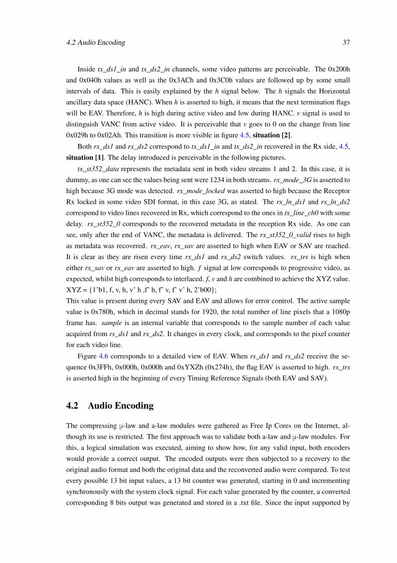
viii
Contents
1 Introduction 11.1 Background . . . . . . . . . . . . . . . . . . . . . . . . . . . . . . . . . . . . . 11.2 Motivation . . . . . . . . . . . . . . . . . . . . . . . . . . . . . . . . . . . . . . 31.3 Dissertation Objectives . . . . . . . . . . . . . . . . . . . . . . . . . . . . . . . 41.4 Dissertation Structure . . . . . . . . . . . . . . . . . . . . . . . . . . . . . . . . 4
2 Technical Framework and State of the Art 52.1 Serial Digital Interface . . . . . . . . . . . . . . . . . . . . . . . . . . . . . . . 52.2 Video formats - Containers and Codecs . . . . . . . . . . . . . . . . . . . . . . 62.3 Video transport over SDI . . . . . . . . . . . . . . . . . . . . . . . . . . . . . . 72.4 3G-SDI - SMPTE ST424 and SMPTE ST425 . . . . . . . . . . . . . . . . . . . 92.5 Metadata - SMPTE ST352 . . . . . . . . . . . . . . . . . . . . . . . . . . . . . 112.6 Random-Access Memories . . . . . . . . . . . . . . . . . . . . . . . . . . . . . 122.7 DDR SDRAM - Double data rate synchronous dynamic random-access memory . 122.8 The SMPTE UHD-SDI IP Core - Basics . . . . . . . . . . . . . . . . . . . . . . 142.9 A-law and μ-law . . . . . . . . . . . . . . . . . . . . . . . . . . . . . . . . . . . 172.10 10 Gb Ethernet Solutions . . . . . . . . . . . . . . . . . . . . . . . . . . . . . . 182.11 Video Over IP solutions . . . . . . . . . . . . . . . . . . . . . . . . . . . . . . . 202.12 Dynamic Reconfiguration . . . . . . . . . . . . . . . . . . . . . . . . . . . . . . 20
3 Requirements Analysis 233.1 Global Overview . . . . . . . . . . . . . . . . . . . . . . . . . . . . . . . . . . 233.2 Design Alternatives . . . . . . . . . . . . . . . . . . . . . . . . . . . . . . . . . 243.3 System Scalability . . . . . . . . . . . . . . . . . . . . . . . . . . . . . . . . . 253.4 Project Constraints . . . . . . . . . . . . . . . . . . . . . . . . . . . . . . . . . 273.5 Validation Plan . . . . . . . . . . . . . . . . . . . . . . . . . . . . . . . . . . . 29
4 Implementation 314.1 The SMPTE UHD-SDI IP Core - Simulation . . . . . . . . . . . . . . . . . . . . 314.2 Audio Encoding . . . . . . . . . . . . . . . . . . . . . . . . . . . . . . . . . . . 374.3 Data Selection . . . . . . . . . . . . . . . . . . . . . . . . . . . . . . . . . . . . 394.4 MIG - Memory Interface Generator . . . . . . . . . . . . . . . . . . . . . . . . 414.5 SMPTE 2022-6 . . . . . . . . . . . . . . . . . . . . . . . . . . . . . . . . . . . 484.6 Chapter Summary . . . . . . . . . . . . . . . . . . . . . . . . . . . . . . . . . . 52
5 Functional Verification 535.1 Implementation Changes . . . . . . . . . . . . . . . . . . . . . . . . . . . . . . 535.2 GTX Transceivers . . . . . . . . . . . . . . . . . . . . . . . . . . . . . . . . . . 54
ix
x CONTENTS
5.3 The SMPTE UHD-SDI IP CORE - Physical Interface . . . . . . . . . . . . . . . 575.4 Pseudo-Video Signal Generator . . . . . . . . . . . . . . . . . . . . . . . . . . . 615.5 ILA – Integrated Logic Analyzer . . . . . . . . . . . . . . . . . . . . . . . . . . 615.6 Dynamic Partial Reconfiguration . . . . . . . . . . . . . . . . . . . . . . . . . . 635.7 Loopback System Verification . . . . . . . . . . . . . . . . . . . . . . . . . . . 675.8 Chapter Summary . . . . . . . . . . . . . . . . . . . . . . . . . . . . . . . . . . 69
6 Conclusions 716.1 Work Summary . . . . . . . . . . . . . . . . . . . . . . . . . . . . . . . . . . . 716.2 Future Work . . . . . . . . . . . . . . . . . . . . . . . . . . . . . . . . . . . . . 72
References 75
List of Figures
1.1 The SDI electrical specification . . . . . . . . . . . . . . . . . . . . . . . . . . . 2
2.1 Television and Video Resolutions . . . . . . . . . . . . . . . . . . . . . . . . . . 72.2 Chroma subsampling . . . . . . . . . . . . . . . . . . . . . . . . . . . . . . . . 72.3 4K and 8K binary ratios . . . . . . . . . . . . . . . . . . . . . . . . . . . . . . . 92.4 How raw 3G-SDI video is transported . . . . . . . . . . . . . . . . . . . . . . . 102.5 SMPTE 424 standard . . . . . . . . . . . . . . . . . . . . . . . . . . . . . . . . 102.6 HANC, VANC and Active Picture video areas . . . . . . . . . . . . . . . . . . . 112.7 SMPTE 352 standard . . . . . . . . . . . . . . . . . . . . . . . . . . . . . . . . 122.8 How DDR technology works . . . . . . . . . . . . . . . . . . . . . . . . . . . . 132.9 SDI Interface . . . . . . . . . . . . . . . . . . . . . . . . . . . . . . . . . . . . 142.10 Receiver Block internal organization . . . . . . . . . . . . . . . . . . . . . . . . 152.11 Transmitter Block internal organization . . . . . . . . . . . . . . . . . . . . . . 162.12 A detailed view of the Ethernet Layer . . . . . . . . . . . . . . . . . . . . . . . 182.13 The XAUI interface . . . . . . . . . . . . . . . . . . . . . . . . . . . . . . . . . 19
3.1 Behavioral Diagram of the conversion platform to be implemented . . . . . . . . 243.2 Blocks Diagram of the conversion platform . . . . . . . . . . . . . . . . . . . . 253.3 Alternative Blocks Diagram of the conversion platform . . . . . . . . . . . . . . 253.4 A 1080p frame can be seen a quarter of a 4K frame . . . . . . . . . . . . . . . . 263.5 4K system uses 4 HD (1080p) inputs . . . . . . . . . . . . . . . . . . . . . . . 263.6 8K system uses 4 UHD1 (4K) inputs . . . . . . . . . . . . . . . . . . . . . . . 273.7 The Virtex VC7203 board . . . . . . . . . . . . . . . . . . . . . . . . . . . . . 283.8 Blocks diagram of the final design to be implemented . . . . . . . . . . . . . . . 293.9 Loopback solution to validate the designed system . . . . . . . . . . . . . . . . . 30
4.1 The SMPTE UHD-SDI Testbench diagram of blocks . . . . . . . . . . . . . . . 324.2 Usage example for the Rx and Tx modules inside the SMPTE UHD-SDI . . . . . 344.3 Global view of 1080p video transmission and reception . . . . . . . . . . . . . . 344.4 Video lines being transmitted through 3G-SDI . . . . . . . . . . . . . . . . . . . 354.5 End of active video . . . . . . . . . . . . . . . . . . . . . . . . . . . . . . . . . 354.6 End of active video, plus CRC . . . . . . . . . . . . . . . . . . . . . . . . . . . 364.7 A-law data compression and recovery . . . . . . . . . . . . . . . . . . . . . . . 384.8 μ-law data compression and recovery . . . . . . . . . . . . . . . . . . . . . . . . 384.9 System designed to validate audio encoding blocks . . . . . . . . . . . . . . . . 394.10 State Machine for Metadata detection by analysing both video data streams . . . 414.11 MIG User Interface and its layers . . . . . . . . . . . . . . . . . . . . . . . . . . 424.12 Write and Read example . . . . . . . . . . . . . . . . . . . . . . . . . . . . . . 444.13 Succession of video data writes and reads . . . . . . . . . . . . . . . . . . . . . 44
xi
xii LIST OF FIGURES
4.14 Start of write requests and delay until first reads . . . . . . . . . . . . . . . . . . 444.15 The User Interface Testbench for DDR3 Ram . . . . . . . . . . . . . . . . . . . 454.16 Standard address space format . . . . . . . . . . . . . . . . . . . . . . . . . . . 464.17 Interleaved address space format . . . . . . . . . . . . . . . . . . . . . . . . . . 474.18 Memory Mapping . . . . . . . . . . . . . . . . . . . . . . . . . . . . . . . . . . 474.19 The SMPTE 2022-6 partial Datagram format . . . . . . . . . . . . . . . . . . . 484.20 The RTP complete Datagram format . . . . . . . . . . . . . . . . . . . . . . . . 494.21 Detailed RTP Header . . . . . . . . . . . . . . . . . . . . . . . . . . . . . . . . 494.22 SMPTE 2022-6 Payload Header . . . . . . . . . . . . . . . . . . . . . . . . . . 494.23 The SMPTE 2022-6 Payload . . . . . . . . . . . . . . . . . . . . . . . . . . . . 504.24 The state machine implemented in the developed SMPTE 2022-6 core . . . . . . 504.25 Network layers required for the complete implementation of the SMPTE 2022-6
protocol . . . . . . . . . . . . . . . . . . . . . . . . . . . . . . . . . . . . . . . 52
5.1 GTX transceivers internal diagram . . . . . . . . . . . . . . . . . . . . . . . . . 555.2 Transceivers connection pad . . . . . . . . . . . . . . . . . . . . . . . . . . . . 575.3 SDI electrical input interface . . . . . . . . . . . . . . . . . . . . . . . . . . . . 585.4 SDI electrical output interface . . . . . . . . . . . . . . . . . . . . . . . . . . . 585.5 SMPTE UHD-SDI Transceiver interface . . . . . . . . . . . . . . . . . . . . . . 595.6 Video Generator Validation . . . . . . . . . . . . . . . . . . . . . . . . . . . . . 615.7 ILA core usage . . . . . . . . . . . . . . . . . . . . . . . . . . . . . . . . . . . 635.8 Partial reconfiguration usage in the audio encoding block . . . . . . . . . . . . . 645.9 Encoding video stream 2 using μ-law . . . . . . . . . . . . . . . . . . . . . . . . 655.10 Encoding video stream 2 using a-law . . . . . . . . . . . . . . . . . . . . . . . . 665.11 Partial Reconfiguration complete system possibility - not implemented . . . . . . 675.12 Implemented SDI interface . . . . . . . . . . . . . . . . . . . . . . . . . . . . . 685.13 Loopback connection between RX-TX . . . . . . . . . . . . . . . . . . . . . . . 685.14 Loopback Validation Results . . . . . . . . . . . . . . . . . . . . . . . . . . . . 695.15 Complete SMPTE UHD-SDI logic interface resource use . . . . . . . . . . . . . 69
6.1 The 425-3 and 425-5 SMPTE standards to define 4K frame using four sub-images 73
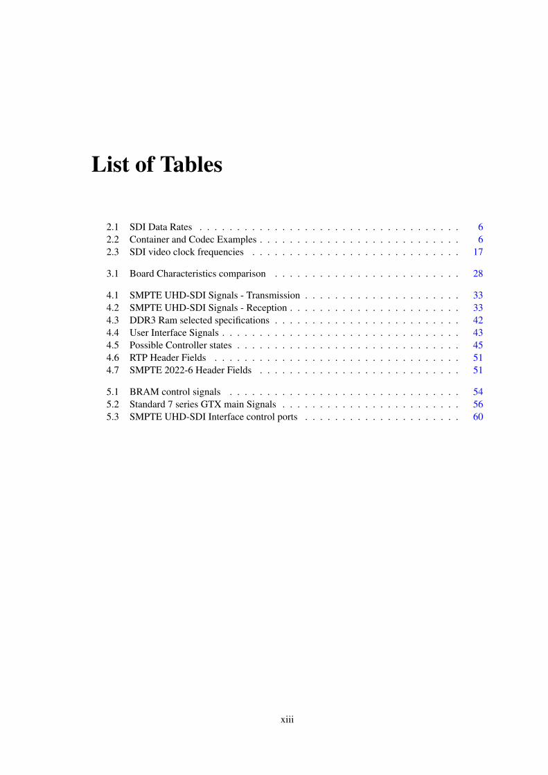
List of Tables
2.1 SDI Data Rates . . . . . . . . . . . . . . . . . . . . . . . . . . . . . . . . . . . 62.2 Container and Codec Examples . . . . . . . . . . . . . . . . . . . . . . . . . . . 62.3 SDI video clock frequencies . . . . . . . . . . . . . . . . . . . . . . . . . . . . 17
3.1 Board Characteristics comparison . . . . . . . . . . . . . . . . . . . . . . . . . 28
4.1 SMPTE UHD-SDI Signals - Transmission . . . . . . . . . . . . . . . . . . . . . 334.2 SMPTE UHD-SDI Signals - Reception . . . . . . . . . . . . . . . . . . . . . . . 334.3 DDR3 Ram selected specifications . . . . . . . . . . . . . . . . . . . . . . . . . 424.4 User Interface Signals . . . . . . . . . . . . . . . . . . . . . . . . . . . . . . . . 434.5 Possible Controller states . . . . . . . . . . . . . . . . . . . . . . . . . . . . . . 454.6 RTP Header Fields . . . . . . . . . . . . . . . . . . . . . . . . . . . . . . . . . 514.7 SMPTE 2022-6 Header Fields . . . . . . . . . . . . . . . . . . . . . . . . . . . 51
5.1 BRAM control signals . . . . . . . . . . . . . . . . . . . . . . . . . . . . . . . 545.2 Standard 7 series GTX main Signals . . . . . . . . . . . . . . . . . . . . . . . . 565.3 SMPTE UHD-SDI Interface control ports . . . . . . . . . . . . . . . . . . . . . 60
xiii

xiv LIST OF TABLES
Abbreviations and Acronyms
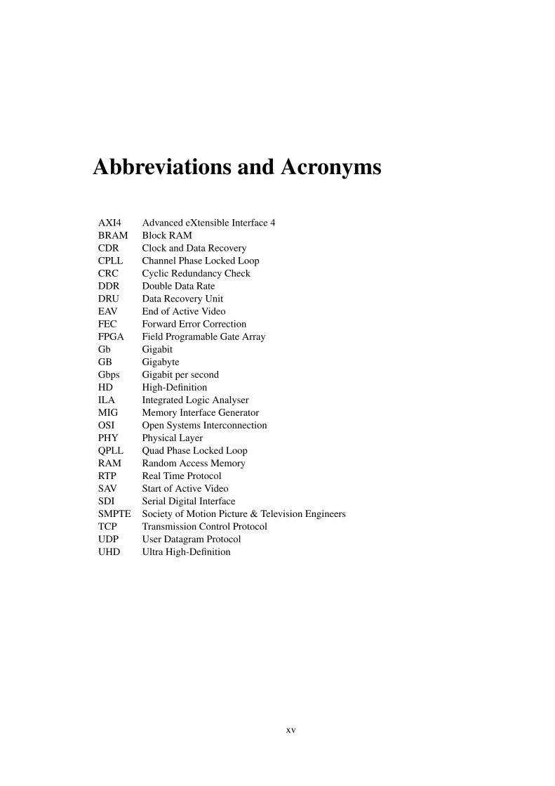
AXI4 Advanced eXtensible Interface 4BRAM Block RAMCDR Clock and Data RecoveryCPLL Channel Phase Locked LoopCRC Cyclic Redundancy CheckDDR Double Data RateDRU Data Recovery UnitEAV End of Active VideoFEC Forward Error CorrectionFPGA Field Programable Gate ArrayGb GigabitGB GigabyteGbps Gigabit per secondHD High-DefinitionILA Integrated Logic AnalyserMIG Memory Interface GeneratorOSI Open Systems InterconnectionPHY Physical LayerQPLL Quad Phase Locked LoopRAM Random Access MemoryRTP Real Time ProtocolSAV Start of Active VideoSDI Serial Digital InterfaceSMPTE Society of Motion Picture & Television EngineersTCP Transmission Control ProtocolUDP User Datagram ProtocolUHD Ultra High-Definition
xv

Chapter 1
Introduction
1.1 Background
Nowadays society is controlled by and dependent on electronic technologies in a way that could
deprive people from comfort and quality of life if a computer or controller somewhere goes wrong.
But, in the same way that technology provides basic services and critical features, namely on the
telecommunications branch, it also branches out into leisure and convenience services. Societies
live over a layer of abstraction provided by technological evolution and their demands on quality
of services increase on the same ratio as technological evolution.
When electronic colour was introduced in the market, in 1953 [1], its high price and the lack of
colour programming slowed down its acceptance into the industry of television. Video colour
was considered a luxury that had no major importance and consumed too many resources, when
compared to the wonders that a video camera, a broadcast system and a television could do, even
if in black & white.
Demands have risen, past technological advances have soon evolved into legacy and an endless
hunger for better video quality has started to take over the industry. Video resolution has been
growing year past year. Plenty of video service providers offer now 4K video and television to
masses. And studies have shown that sales of 4K televisions are increasing year past year [2][3].
Video studios must adapt to distribution demands and in opposition to the past, where video was
captured in high quality but distributed heavily compressed [4], nowadays the distribution can be
as demanding as the capture. Video studios are in charge for editing and incorporating ancillary
information to the video streams and that process must be performed many times in real time.
Therefore, broadcasting real time, high resolution video signals demands editing and transporting
uncompressed video data prior to its encoding and distribution.
The standard industry interface for transporting uncompressed video streams is the Serial Dig-
ital Interface, commonly known as SDI. “SDI has become the ubiquitous interface standard within
the professional broadcast industry and the success of SDI is due in no part to a number of specific
characteristics: ability to transport uncompressed signals, low latency, cost-effective implementa-
tion, robustness and reliability, seamless interoperability, reuse of existing infrastructure [5]."
1
2 Introduction
In 2015 the SDI 12G mode was standardized by SMPTE. This means that video captured data
at more than 12 Gbps must be transported in more than one SDI cable, and prior to the 12G stan-
dardization, SDI data ratios could only reach the 6Gbps. SDI is a legacy video transport connected
directly to the capture device that uses coax cable and 75 Ohm terminal BNC connectors. One of
the major limiting factors when it comes to sending data over copper cables is the Skin Effect,
which consists of increased attenuation as the frequency of the signal increases [5]. Dielectric loss
and impedance mismatches at connectors also limit cable length performance at high bit rates [6].
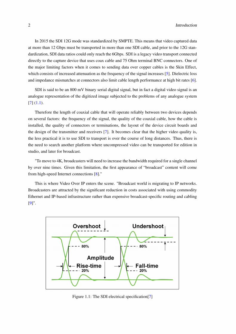
SDI is said to be an 800 mV binary serial digital signal, but in fact a digital video signal is an
analogue representation of the digitized image subjected to the problems of any analogue system
[7] (1.1).
Therefore the length of coaxial cable that will operate reliably between two devices depends
on several factors: the frequency of the signal, the quality of the coaxial cable, how the cable is
installed, the quality of connectors or terminations, the layout of the device circuit boards and
the design of the transmitter and receivers [7]. It becomes clear that the higher video quality is,
the less practical it is to use SDI to transport is over the course of long distances. Thus, there is
the need to search another platform where uncompressed video can be transported for edition in
studio, and later for broadcast.
"To move to 4K, broadcasters will need to increase the bandwidth required for a single channel
by over nine times. Given this limitation, the first appearance of “broadcast” content will come
from high-speed Internet connections [8]."
This is where Video Over IP enters the scene. "Broadcast world is migrating to IP networks.
Broadcasters are attracted by the significant reduction in costs associated with using commodity
Ethernet and IP-based infrastructure rather than expensive broadcast-specific routing and cabling
[9]".
Figure 1.1: The SDI electrical specification[7]
1.2 Motivation 3
1.2 Motivation
High Definition and Ultra High Definition video resolutions require high performance processing
due to its high bit rates. Most HD solutions combine the usage of some dedicated hardware [10]
(such as video capture boards) and powerful computer processing. However, with the emerging
of UHD, the restrictions and difficulties of maintaining a processing system in charge of a studio
video system increase exponentially. With Moore’s law on the verge of failing [11] [12], devel-
opers invest on parallel processing (multiple cores) and other hardware prediction techniques to
make up for limitations and allow for better performance processors. However, this is a problem
that can easily be solved with dedicated hardware.
In a dedicated task such as converting between video platforms, dedicated hardware is the
most effective solution because it grants better performance, lesser space and optimizes energy
usage. Above all, the final solution will provide video editors with transport and studio distribution
advantages in terms of speed, reliability and platform flexibility without disregarding the legacy
platforms.
Field Programmable Gate Arrays are commercially available since 1985 and allow hardware
prototyping compatible to a vast range of peripherals and external integration. They are designed
to be configured after production. This corresponds to the most flexible hardware configurable
platform available in the field.
As [13] underlines, "technically speaking, an FPGA can solve any computable problem. This
is trivially proven by the fact that an FPGA can be used to implement a soft microprocessor". This
also underlines the fact that software is no more than an abstraction aimed to control hardware.
This project aims to build a base pillar for platform transition of uncompressed High Definition
video. It was realized taking into account 1080p and 4K video specifications and scalability to
more demanding systems and the incorporation of more complex features.
Converting between video platforms using dedicated hardware demands the usage of multiple
tools, in the most diverse telecommunication fields, such as: Multimedia, Microelectronics and
Computer Networks. System requirements demand the use of several IP Cores and compatibility
with a wide set of standards, both for video (SMPTE) and IP networks. Hardware implementa-
tions always open up a wide range of possibilities and implementation alternatives that were also
analyzed and had into account during the development of the project.
MOG Technologies is in the field of video industry ingest solutions, offering high performance
real time solutions to broadcasters and video editors. Most of the company solutions are software
based. This project emerges as a technology prospection to give insight into the problems and
solutions faced and found when dealing with FPGA and hardware solutions, aiming for future
investments and market approaches. The insight acquired on the existing IP Cores, market tools
and possible implementation approaches as well as verification methods, is of great value to allow
a proper analysis if the course is to be set on this field.
4 Introduction
1.3 Dissertation Objectives
The project developed for this dissertation aims to study about the feasibility of a dedicated solu-
tion capable of real time conversion between uncompressed HD video transporting platforms (SDI
to IP). It is intended to:
• Analyze the different High Definition formats, specifications and data ratios common in the
industry and to select suitable components to deal with its characteristics.
• Analyze and describe how a viable solution could be scalable and upgraded into more com-
plex systems. The whole design is made based on this principle.
• Analyze what video compatible tools are available on the reconfigurable hardware market
and focus on their study, usage and implementation.
• Conceive, design and construct a dedicated system capable of converting video transport
platforms, assembling the required tools.
• Describe and solve problems and their variants faced during the implementation of a work-
ing prototype.
• Conclude about the feasibility of a real time assembled working prototype, implementing a
wide range of tools and telecommunication domain areas.
1.4 Dissertation Structure
This dissertation is organized as follows:
• Chapter 2 - Technical framework and State of the Art: This chapter introduces some theoret-
ical concepts related to uncompressed video, its transport and formats, as well as researched
tools and technological fields required to assemble a proposed design.
• Chapter 3 - Requirements Analysis: In this chapter, the system requirements and available
resources are analysed and a balanced decision on the system to be implemented is made.
• Chapter 4 - Implementation: This chapter describes how the system components were im-
plemented on the assembled design and also gives a technical overview on how each of them
behaves through simulation.
• Chapter 5 - Functional Verification: This chapter describes how the system was validated
through the building of a prototype, how the physical implementation differs from the sim-
ulated implementation and how the physical prototype was assembled.
• Chapter 6 - Conclusions: This chapter presents a set of future work possibilities as well as
some details on how they could be implemented, and a summary about the implemented
work and the obtained results.
Chapter 2
Technical Framework and State of theArt
In this chapter the tools and standards used and studied in the development of this project as well
as related knowledge areas are briefly explained to allow a proper understanding of the design
proposed and of the implemented prototype. This chapter presents the reader to main concepts,
such as the uncompressed video formats and specifications, video transport, video interfaces and
the relationship and impact between different resolutions. It gives also some insight on the Xilinx
solutions suitable to be used, such as the SMPTE UHD-SDI, the DDR MIG controller and the
10Gb Ethernet IP Core. Knowledge areas such as RAM memories and the DDR technology, dy-
namic partial reconfiguration, network layer protocols, video transport over IP and audio encoding
are also approached and explained.
2.1 Serial Digital Interface
Serial digital interface (SDI) refers to a family of interfaces standardized by SMPTE (The Society
of Motion Picture and Television Engineers). The data stream is serialized, then subjected to
a scrambling technique. "SDI is standardized for electrical transmission through coaxial cable,
and for transmission through optical fiber"[4]. "The SDI electrical interface uses ECL (Emitter-
Coupled Logic) levels, 75 Ohms impedance, BNC connectors, and coaxial cable"[4].
SDI transmits uncompressed data streams. "Compressed digital video interfaces are impracti-
cal in the studio owing to the diversity of compression systems, and because compressed interfaces
would require decompression capabilities in signal processing and monitoring equipment"[4].
In the transport of digital video, ancillary data is also a critical resource. Ancillary data packets
are used to transmit non-video information (such as digital audio, closed captioning, teletext,
timecodes, metadata, etc.) during the blanking intervals. A wide variety of ITU-R and SMPTE
specifications describe the various ancillary data formats[14]. Metadata on HD video formats
follows the SMPTE ST-352 standard [15].
5
6 Technical Framework and State of the Art
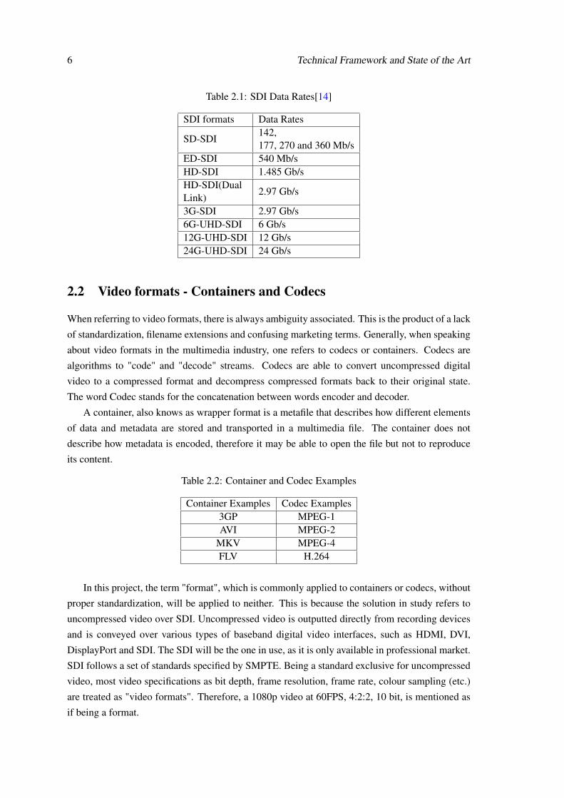
Table 2.1: SDI Data Rates[14]
SDI formats Data Rates
SD-SDI142,177, 270 and 360 Mb/s
ED-SDI 540 Mb/sHD-SDI 1.485 Gb/sHD-SDI(DualLink)
2.97 Gb/s
3G-SDI 2.97 Gb/s6G-UHD-SDI 6 Gb/s12G-UHD-SDI 12 Gb/s24G-UHD-SDI 24 Gb/s
2.2 Video formats - Containers and Codecs
When referring to video formats, there is always ambiguity associated. This is the product of a lack
of standardization, filename extensions and confusing marketing terms. Generally, when speaking
about video formats in the multimedia industry, one refers to codecs or containers. Codecs are
algorithms to "code" and "decode" streams. Codecs are able to convert uncompressed digital
video to a compressed format and decompress compressed formats back to their original state.
The word Codec stands for the concatenation between words encoder and decoder.
A container, also knows as wrapper format is a metafile that describes how different elements
of data and metadata are stored and transported in a multimedia file. The container does not
describe how metadata is encoded, therefore it may be able to open the file but not to reproduce
its content.
Table 2.2: Container and Codec Examples
Container Examples Codec Examples3GP MPEG-1AVI MPEG-2
MKV MPEG-4FLV H.264
In this project, the term "format", which is commonly applied to containers or codecs, without
proper standardization, will be applied to neither. This is because the solution in study refers to
uncompressed video over SDI. Uncompressed video is outputted directly from recording devices
and is conveyed over various types of baseband digital video interfaces, such as HDMI, DVI,
DisplayPort and SDI. The SDI will be the one in use, as it is only available in professional market.
SDI follows a set of standards specified by SMPTE. Being a standard exclusive for uncompressed
video, most video specifications as bit depth, frame resolution, frame rate, colour sampling (etc.)
are treated as "video formats". Therefore, a 1080p video at 60FPS, 4:2:2, 10 bit, is mentioned as
if being a format.
2.3 Video transport over SDI 7
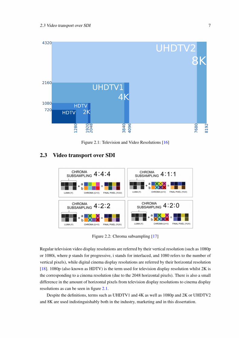
Figure 2.1: Television and Video Resolutions [16]
2.3 Video transport over SDI
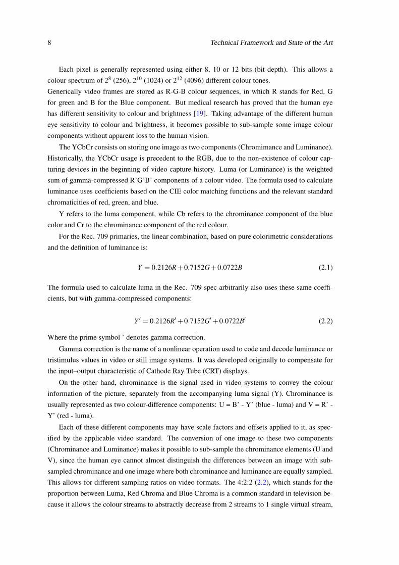
Figure 2.2: Chroma subsampling [17]
Regular television video display resolutions are referred by their vertical resolution (such as 1080p
or 1080i, where p stands for progressive, i stands for interlaced, and 1080 refers to the number of
vertical pixels), while digital cinema display resolutions are referred by their horizontal resolution
[18]. 1080p (also known as HDTV) is the term used for television display resolution whilst 2K is
the corresponding to a cinema resolution (due to the 2048 horizontal pixels). There is also a small
difference in the amount of horizontal pixels from television display resolutions to cinema display
resolutions as can be seen in figure 2.1.
Despite the definitions, terms such as UHDTV1 and 4K as well as 1080p and 2K or UHDTV2
and 8K are used indistinguishably both in the industry, marketing and in this dissertation.
8 Technical Framework and State of the Art
Each pixel is generally represented using either 8, 10 or 12 bits (bit depth). This allows a
colour spectrum of 28 (256), 210 (1024) or 212 (4096) different colour tones.
Generically video frames are stored as R-G-B colour sequences, in which R stands for Red, G
for green and B for the Blue component. But medical research has proved that the human eye
has different sensitivity to colour and brightness [19]. Taking advantage of the different human
eye sensitivity to colour and brightness, it becomes possible to sub-sample some image colour
components without apparent loss to the human vision.
The YCbCr consists on storing one image as two components (Chromimance and Luminance).
Historically, the YCbCr usage is precedent to the RGB, due to the non-existence of colour cap-
turing devices in the beginning of video capture history. Luma (or Luminance) is the weighted
sum of gamma-compressed R’G’B’ components of a colour video. The formula used to calculate
luminance uses coefficients based on the CIE color matching functions and the relevant standard
chromaticities of red, green, and blue.
Y refers to the luma component, while Cb refers to the chrominance component of the blue
color and Cr to the chrominance component of the red colour.
For the Rec. 709 primaries, the linear combination, based on pure colorimetric considerations
and the definition of luminance is:
Y = 0.2126R+0.7152G+0.0722B (2.1)
The formula used to calculate luma in the Rec. 709 spec arbitrarily also uses these same coeffi-
cients, but with gamma-compressed components:
Y ′ = 0.2126R′+0.7152G′+0.0722B′ (2.2)
Where the prime symbol ’ denotes gamma correction.
Gamma correction is the name of a nonlinear operation used to code and decode luminance or
tristimulus values in video or still image systems. It was developed originally to compensate for
the input–output characteristic of Cathode Ray Tube (CRT) displays.
On the other hand, chrominance is the signal used in video systems to convey the colour
information of the picture, separately from the accompanying luma signal (Y). Chrominance is
usually represented as two colour-difference components: U = B’ - Y’ (blue - luma) and V = R’ -
Y’ (red - luma).
Each of these different components may have scale factors and offsets applied to it, as spec-
ified by the applicable video standard. The conversion of one image to these two components
(Chrominance and Luminance) makes it possible to sub-sample the chrominance elements (U and
V), since the human eye cannot almost distinguish the differences between an image with sub-
sampled chrominance and one image where both chrominance and luminance are equally sampled.
This allows for different sampling ratios on video formats. The 4:2:2 (2.2), which stands for the
proportion between Luma, Red Chroma and Blue Chroma is a common standard in television be-
cause it allows the colour streams to abstractly decrease from 2 streams to 1 single virtual stream,
2.4 3G-SDI - SMPTE ST424 and SMPTE ST425 9
since both streams are sub-sampled and can be multiplexed together. Therefore, 4:2:2 corresponds
to 2 colour channels.
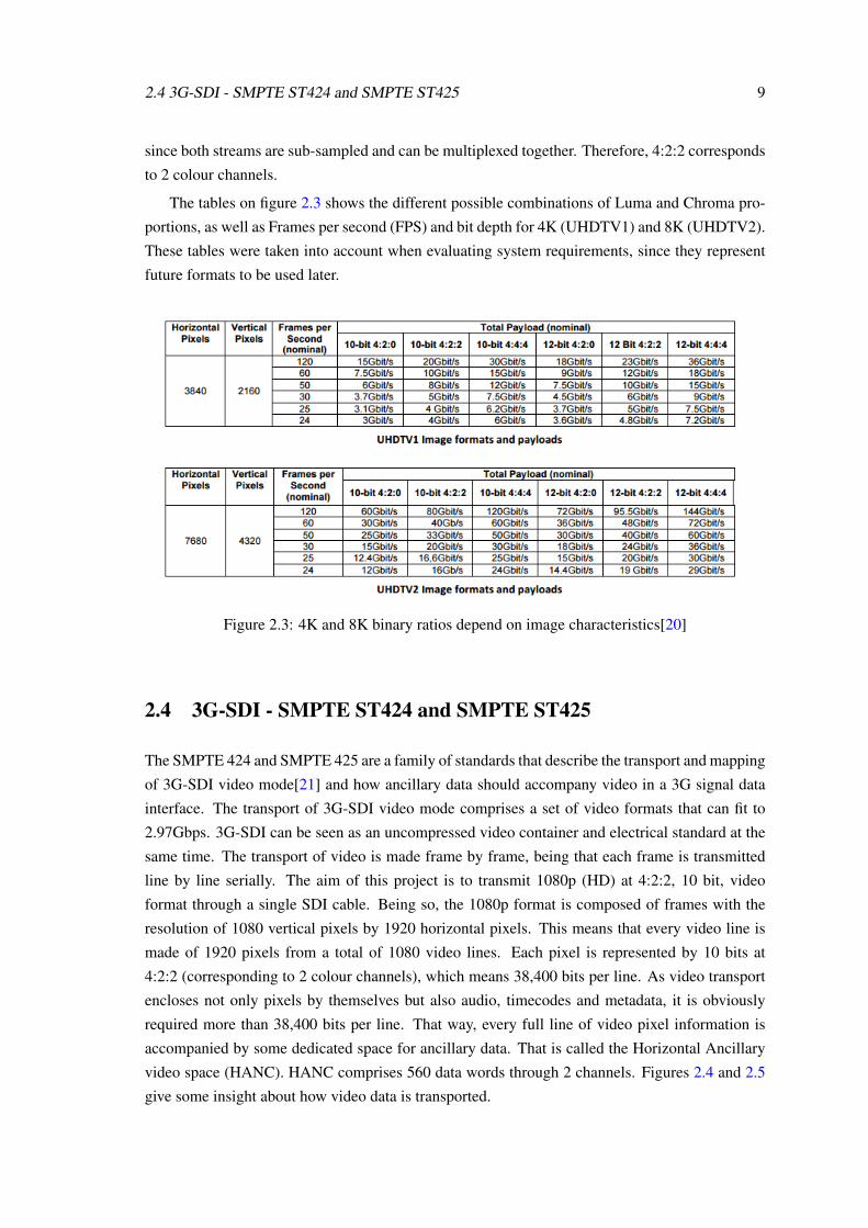
The tables on figure 2.3 shows the different possible combinations of Luma and Chroma pro-
portions, as well as Frames per second (FPS) and bit depth for 4K (UHDTV1) and 8K (UHDTV2).
These tables were taken into account when evaluating system requirements, since they represent
future formats to be used later.
Figure 2.3: 4K and 8K binary ratios depend on image characteristics[20]
2.4 3G-SDI - SMPTE ST424 and SMPTE ST425
The SMPTE 424 and SMPTE 425 are a family of standards that describe the transport and mapping
of 3G-SDI video mode[21] and how ancillary data should accompany video in a 3G signal data
interface. The transport of 3G-SDI video mode comprises a set of video formats that can fit to
2.97Gbps. 3G-SDI can be seen as an uncompressed video container and electrical standard at the
same time. The transport of video is made frame by frame, being that each frame is transmitted
line by line serially. The aim of this project is to transmit 1080p (HD) at 4:2:2, 10 bit, video
format through a single SDI cable. Being so, the 1080p format is composed of frames with the
resolution of 1080 vertical pixels by 1920 horizontal pixels. This means that every video line is
made of 1920 pixels from a total of 1080 video lines. Each pixel is represented by 10 bits at
4:2:2 (corresponding to 2 colour channels), which means 38,400 bits per line. As video transport
encloses not only pixels by themselves but also audio, timecodes and metadata, it is obviously
required more than 38,400 bits per line. That way, every full line of video pixel information is
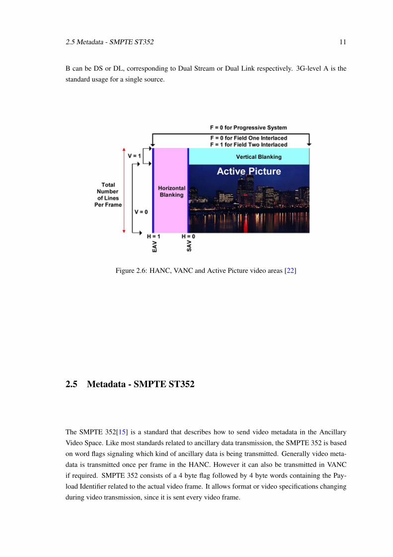
accompanied by some dedicated space for ancillary data. That is called the Horizontal Ancillary
video space (HANC). HANC comprises 560 data words through 2 channels. Figures 2.4 and 2.5
give some insight about how video data is transported.
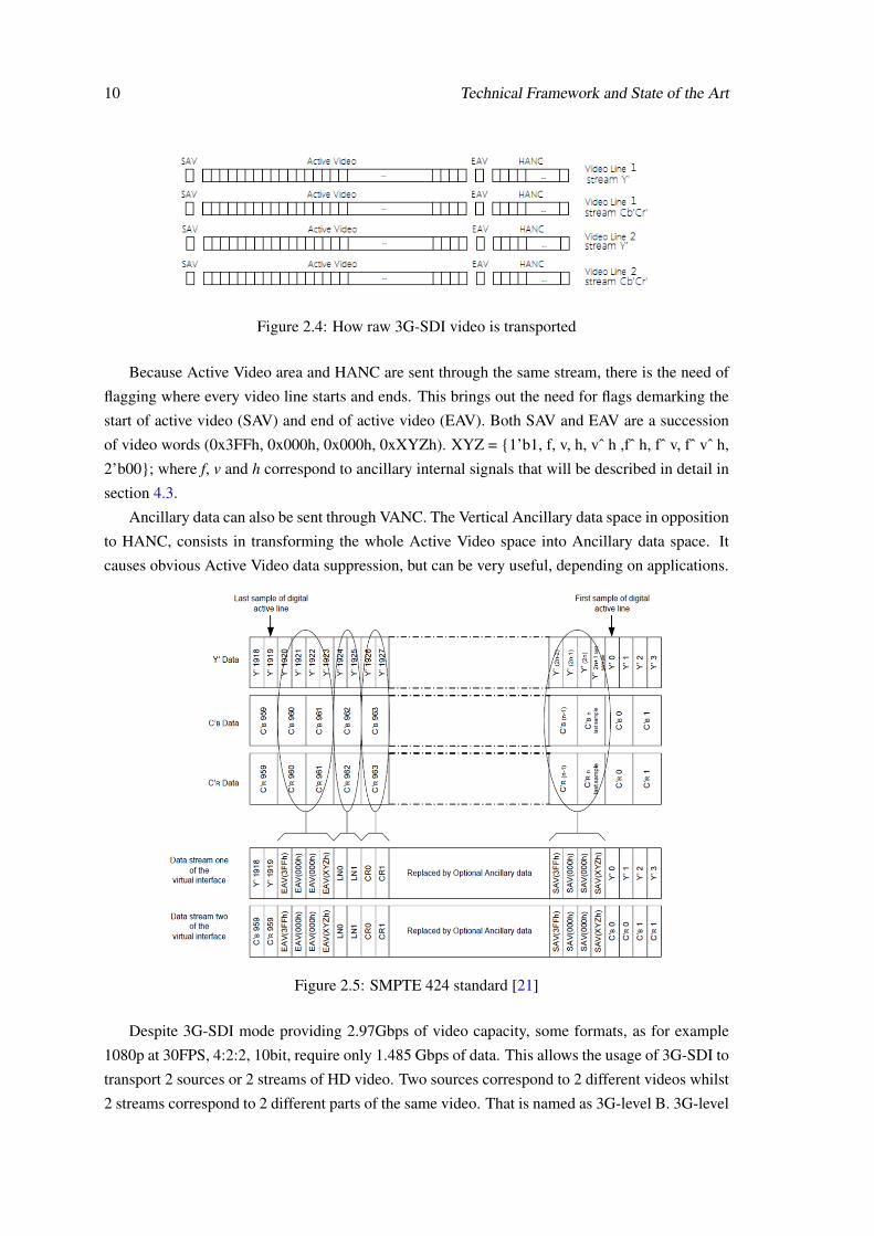
10 Technical Framework and State of the Art
Figure 2.4: How raw 3G-SDI video is transported
Because Active Video area and HANC are sent through the same stream, there is the need of
flagging where every video line starts and ends. This brings out the need for flags demarking the
start of active video (SAV) and end of active video (EAV). Both SAV and EAV are a succession
of video words (0x3FFh, 0x000h, 0x000h, 0xXYZh). XYZ = {1’b1, f, v, h, vˆ h ,fˆ h, fˆ v, fˆ vˆ h,
2’b00}; where f, v and h correspond to ancillary internal signals that will be described in detail in
section 4.3.
Ancillary data can also be sent through VANC. The Vertical Ancillary data space in opposition
to HANC, consists in transforming the whole Active Video space into Ancillary data space. It
causes obvious Active Video data suppression, but can be very useful, depending on applications.
Figure 2.5: SMPTE 424 standard [21]
Despite 3G-SDI mode providing 2.97Gbps of video capacity, some formats, as for example
1080p at 30FPS, 4:2:2, 10bit, require only 1.485 Gbps of data. This allows the usage of 3G-SDI to
transport 2 sources or 2 streams of HD video. Two sources correspond to 2 different videos whilst
2 streams correspond to 2 different parts of the same video. That is named as 3G-level B. 3G-level
2.5 Metadata - SMPTE ST352 11
B can be DS or DL, corresponding to Dual Stream or Dual Link respectively. 3G-level A is the
standard usage for a single source.
Figure 2.6: HANC, VANC and Active Picture video areas [22]
2.5 Metadata - SMPTE ST352
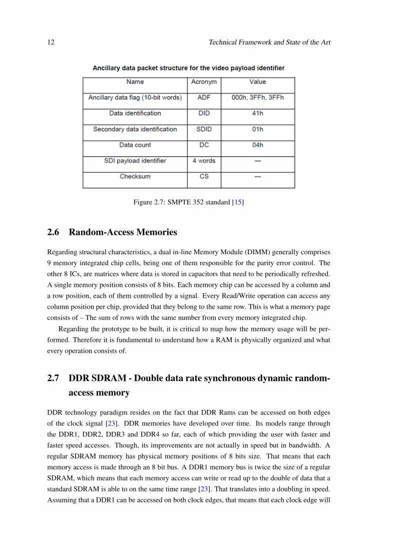
The SMPTE 352[15] is a standard that describes how to send video metadata in the Ancillary
Video Space. Like most standards related to ancillary data transmission, the SMPTE 352 is based
on word flags signaling which kind of ancillary data is being transmitted. Generally video meta-
data is transmitted once per frame in the HANC. However it can also be transmitted in VANC
if required. SMPTE 352 consists of a 4 byte flag followed by 4 byte words containing the Pay-
load Identifier related to the actual video frame. It allows format or video specifications changing
during video transmission, since it is sent every video frame.
12 Technical Framework and State of the Art
Figure 2.7: SMPTE 352 standard [15]
2.6 Random-Access Memories
Regarding structural characteristics, a dual in-line Memory Module (DIMM) generally comprises
9 memory integrated chip cells, being one of them responsible for the parity error control. The
other 8 ICs, are matrices where data is stored in capacitors that need to be periodically refreshed.
A single memory position consists of 8 bits. Each memory chip can be accessed by a column and
a row position, each of them controlled by a signal. Every Read/Write operation can access any
column position per chip, provided that they belong to the same row. This is what a memory page
consists of – The sum of rows with the same number from every memory integrated chip.
Regarding the prototype to be built, it is critical to map how the memory usage will be per-
formed. Therefore it is fundamental to understand how a RAM is physically organized and what
every operation consists of.
2.7 DDR SDRAM - Double data rate synchronous dynamic random-access memory
DDR technology paradigm resides on the fact that DDR Rams can be accessed on both edges
of the clock signal [23]. DDR memories have developed over time. Its models range through
the DDR1, DDR2, DDR3 and DDR4 so far, each of which providing the user with faster and
faster speed accesses. Though, its improvements are not actually in speed but in bandwidth. A
regular SDRAM memory has physical memory positions of 8 bits size. That means that each
memory access is made through an 8 bit bus. A DDR1 memory bus is twice the size of a regular
SDRAM, which means that each memory access can write or read up to the double of data that a
standard SDRAM is able to on the same time range [23]. That translates into a doubling in speed.
Assuming that a DDR1 can be accessed on both clock edges, that means that each clock edge will
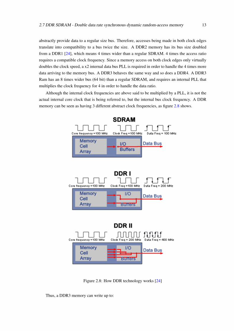
2.7 DDR SDRAM - Double data rate synchronous dynamic random-access memory 13
abstractly provide data to a regular size bus. Therefore, accesses being made in both clock edges
translate into compatibility to a bus twice the size. A DDR2 memory has its bus size doubled
from a DDR1 [24], which means 4 times wider than a regular SDRAM. 4 times the access ratio
requires a compatible clock frequency. Since a memory access on both clock edges only virtually
doubles the clock speed, a x2 internal data bus PLL is required in order to handle the 4 times more
data arriving to the memory bus. A DDR3 behaves the same way and so does a DDR4. A DDR3
Ram has an 8 times wider bus (64 bit) than a regular SDRAM, and requires an internal PLL that
multiplies the clock frequency for 4 in order to handle the data ratio.
Although the internal clock frequencies are above said to be multiplied by a PLL, it is not the
actual internal core clock that is being referred to, but the internal bus clock frequency. A DDR
memory can be seen as having 3 different abstract clock frequencies, as figure 2.8 shows.
Figure 2.8: How DDR technology works [24]
Thus, a DDR3 memory can write up to:
14 Technical Framework and State of the Art
• 8 (regular bus size) x 2 (both clock edges) x 4 (PLL internal frequency) x clock rate, bits per
second,
or
• 64 (bus width) x clock rate, bits per second
That, for a standard 200MHz clock provides a data transfer of 12,800Mbps. At 148.5MHz
clock rate (the frequency used to process 3G video mode), it corresponds to 9,505Mbps. One
frame of 1080p, 4:2:2, 10bit depth uses:
• 1080(rows) x 2200(columns) x 10(bit depth) x 2 (colour channels) = 47.52Mbit per frame
This means a DDR3 Ram could store up to 200 frames per second.
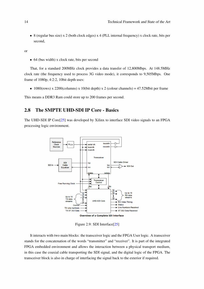
2.8 The SMPTE UHD-SDI IP Core - Basics
The UHD-SDI IP Core[25] was developed by Xilinx to interface SDI video signals to an FPGA
processing logic environment.
Figure 2.9: SDI Interface[25]
It interacts with two main blocks: the transceiver logic and the FPGA User logic. A transceiver
stands for the concatenation of the words “transmitter” and “receiver”. It is part of the integrated
FPGA embedded environment and allows the interaction between a physical transport medium,
in this case the coaxial cable transporting the SDI signal, and the digital logic of the FPGA. The
transceiver block is also in charge of interfacing the signal back to the exterior if required.
2.8 The SMPTE UHD-SDI IP Core - Basics 15
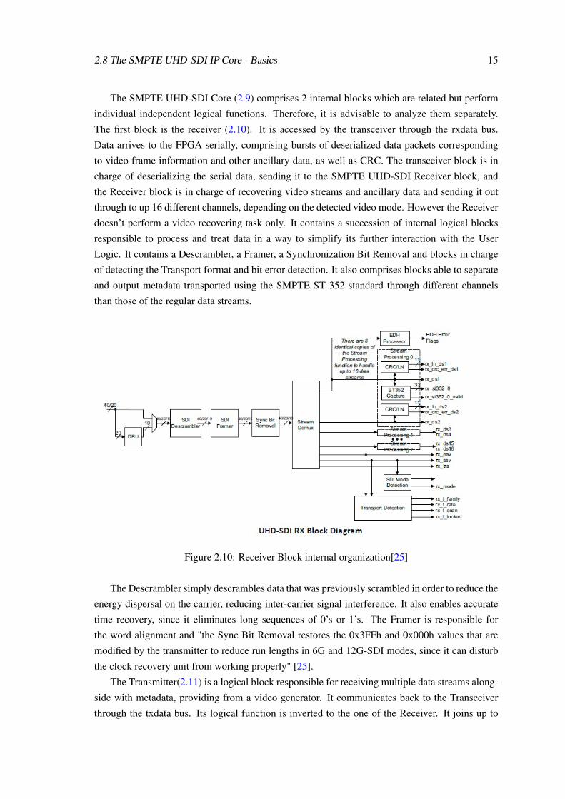
The SMPTE UHD-SDI Core (2.9) comprises 2 internal blocks which are related but perform
individual independent logical functions. Therefore, it is advisable to analyze them separately.
The first block is the receiver (2.10). It is accessed by the transceiver through the rxdata bus.
Data arrives to the FPGA serially, comprising bursts of deserialized data packets corresponding
to video frame information and other ancillary data, as well as CRC. The transceiver block is in
charge of deserializing the serial data, sending it to the SMPTE UHD-SDI Receiver block, and
the Receiver block is in charge of recovering video streams and ancillary data and sending it out
through to up 16 different channels, depending on the detected video mode. However the Receiver
doesn’t perform a video recovering task only. It contains a succession of internal logical blocks
responsible to process and treat data in a way to simplify its further interaction with the User
Logic. It contains a Descrambler, a Framer, a Synchronization Bit Removal and blocks in charge
of detecting the Transport format and bit error detection. It also comprises blocks able to separate
and output metadata transported using the SMPTE ST 352 standard through different channels
than those of the regular data streams.
Figure 2.10: Receiver Block internal organization[25]
The Descrambler simply descrambles data that was previously scrambled in order to reduce the
energy dispersal on the carrier, reducing inter-carrier signal interference. It also enables accurate
time recovery, since it eliminates long sequences of 0’s or 1’s. The Framer is responsible for
the word alignment and "the Sync Bit Removal restores the 0x3FFh and 0x000h values that are
modified by the transmitter to reduce run lengths in 6G and 12G-SDI modes, since it can disturb
the clock recovery unit from working properly" [25].
The Transmitter(2.11) is a logical block responsible for receiving multiple data streams along-
side with metadata, providing from a video generator. It communicates back to the Transceiver
through the txdata bus. Its logical function is inverted to the one of the Receiver. It joins up to
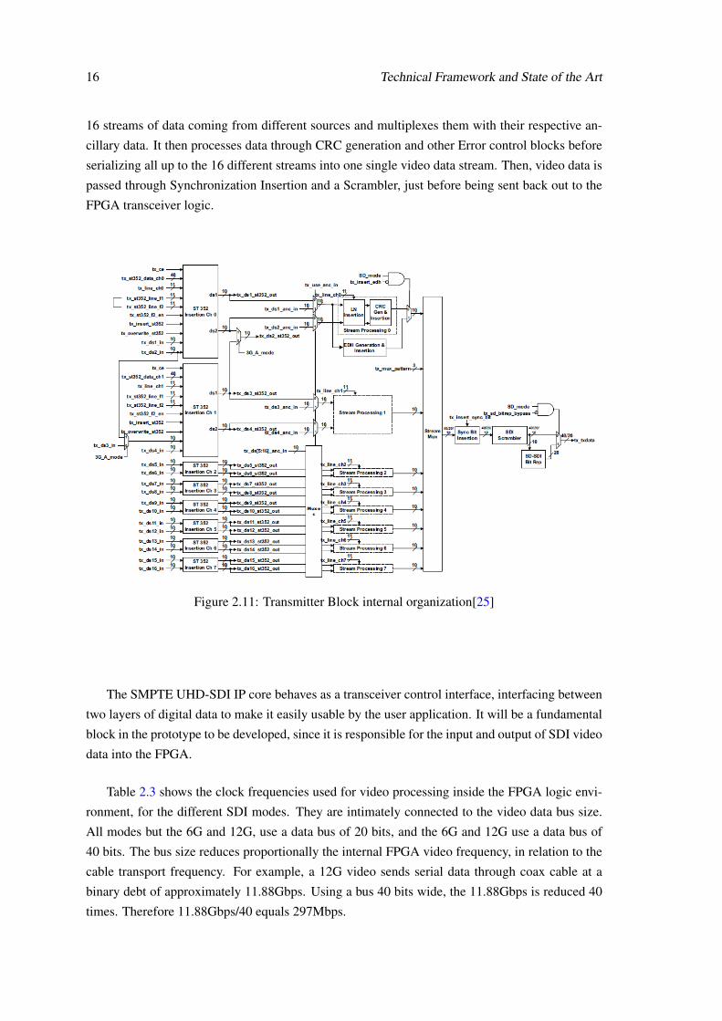
16 Technical Framework and State of the Art
16 streams of data coming from different sources and multiplexes them with their respective an-
cillary data. It then processes data through CRC generation and other Error control blocks before
serializing all up to the 16 different streams into one single video data stream. Then, video data is
passed through Synchronization Insertion and a Scrambler, just before being sent back out to the
FPGA transceiver logic.
Figure 2.11: Transmitter Block internal organization[25]
The SMPTE UHD-SDI IP core behaves as a transceiver control interface, interfacing between
two layers of digital data to make it easily usable by the user application. It will be a fundamental
block in the prototype to be developed, since it is responsible for the input and output of SDI video
data into the FPGA.
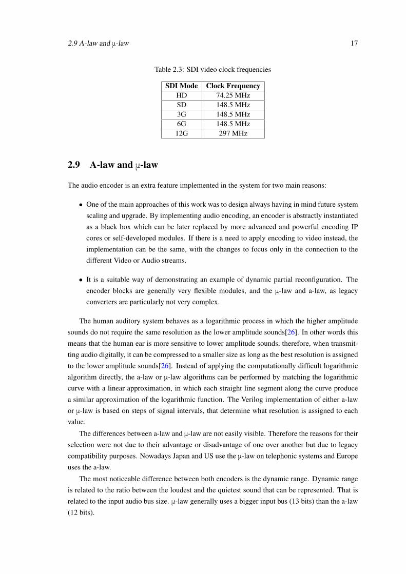
Table 2.3 shows the clock frequencies used for video processing inside the FPGA logic envi-
ronment, for the different SDI modes. They are intimately connected to the video data bus size.
All modes but the 6G and 12G, use a data bus of 20 bits, and the 6G and 12G use a data bus of
40 bits. The bus size reduces proportionally the internal FPGA video frequency, in relation to the
cable transport frequency. For example, a 12G video sends serial data through coax cable at a
binary debt of approximately 11.88Gbps. Using a bus 40 bits wide, the 11.88Gbps is reduced 40
times. Therefore 11.88Gbps/40 equals 297Mbps.
2.9 A-law and μ-law 17
Table 2.3: SDI video clock frequencies
SDI Mode Clock FrequencyHD 74.25 MHzSD 148.5 MHz3G 148.5 MHz6G 148.5 MHz12G 297 MHz
2.9 A-law and μ-law
The audio encoder is an extra feature implemented in the system for two main reasons:
• One of the main approaches of this work was to design always having in mind future system
scaling and upgrade. By implementing audio encoding, an encoder is abstractly instantiated
as a black box which can be later replaced by more advanced and powerful encoding IP
cores or self-developed modules. If there is a need to apply encoding to video instead, the
implementation can be the same, with the changes to focus only in the connection to the
different Video or Audio streams.
• It is a suitable way of demonstrating an example of dynamic partial reconfiguration. The
encoder blocks are generally very flexible modules, and the μ-law and a-law, as legacy
converters are particularly not very complex.
The human auditory system behaves as a logarithmic process in which the higher amplitude
sounds do not require the same resolution as the lower amplitude sounds[26]. In other words this
means that the human ear is more sensitive to lower amplitude sounds, therefore, when transmit-
ting audio digitally, it can be compressed to a smaller size as long as the best resolution is assigned
to the lower amplitude sounds[26]. Instead of applying the computationally difficult logarithmic
algorithm directly, the a-law or μ-law algorithms can be performed by matching the logarithmic
curve with a linear approximation, in which each straight line segment along the curve produce
a similar approximation of the logarithmic function. The Verilog implementation of either a-law
or μ-law is based on steps of signal intervals, that determine what resolution is assigned to each
value.
The differences between a-law and μ-law are not easily visible. Therefore the reasons for their
selection were not due to their advantage or disadvantage of one over another but due to legacy
compatibility purposes. Nowadays Japan and US use the μ-law on telephonic systems and Europe
uses the a-law.
The most noticeable difference between both encoders is the dynamic range. Dynamic range
is related to the ratio between the loudest and the quietest sound that can be represented. That is
related to the input audio bus size. μ-law generally uses a bigger input bus (13 bits) than the a-law
(12 bits).
18 Technical Framework and State of the Art
Because the most important difference is due to the input bus, the usage of both these encoders
only makes sense when coordinated with the analog audio sampling capture system. Due to the
lack of resources, both modules will be used as if different audio encoding blocks, although they
are practically the same. The differences on the input bus size will be overcome by adapting the
a-law encoder to 13 bits.
2.10 10 Gb Ethernet Solutions
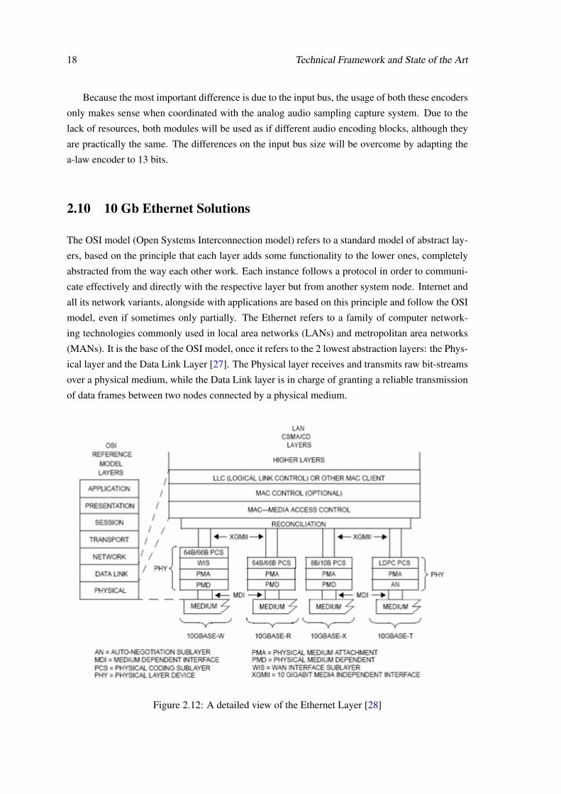
The OSI model (Open Systems Interconnection model) refers to a standard model of abstract lay-
ers, based on the principle that each layer adds some functionality to the lower ones, completely
abstracted from the way each other work. Each instance follows a protocol in order to communi-
cate effectively and directly with the respective layer but from another system node. Internet and
all its network variants, alongside with applications are based on this principle and follow the OSI
model, even if sometimes only partially. The Ethernet refers to a family of computer network-
ing technologies commonly used in local area networks (LANs) and metropolitan area networks
(MANs). It is the base of the OSI model, once it refers to the 2 lowest abstraction layers: the Phys-
ical layer and the Data Link Layer [27]. The Physical layer receives and transmits raw bit-streams
over a physical medium, while the Data Link layer is in charge of granting a reliable transmission
of data frames between two nodes connected by a physical medium.
Figure 2.12: A detailed view of the Ethernet Layer [28]
2.10 10 Gb Ethernet Solutions 19
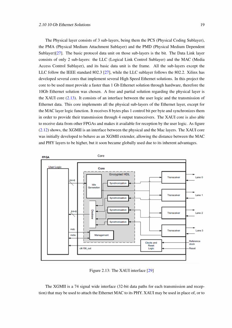
The Physical layer consists of 3 sub-layers, being them the PCS (Physical Coding Sublayer),
the PMA (Physical Medium Attachment Sublayer) and the PMD (Physical Medium Dependent
Sublayer)[27]. The basic protocol data unit on those sub-layers is the bit. The Data Link layer
consists of only 2 sub-layers: the LLC (Logical Link Control Sublayer) and the MAC (Media
Access Control Sublayer), and its basic data unit is the frame. All the sub-layers except the
LLC follow the IEEE standard 802.3 [27], while the LLC sublayer follows the 802.2. Xilinx has
developed several cores that implement several High Speed Ethernet solutions. In this project the
core to be used must provide a faster than 1 Gb Ethernet solution through hardware, therefore the
10Gb Ethernet solution was chosen. A free and partial solution regarding the physical layer is
the XAUI core (2.13). It consists of an interface between the user logic and the transmission of
Ethernet data. This core implements all the physical sub-layers of the Ethernet layer, except for
the MAC layer logic function. It receives 8 bytes plus 1 control bit per byte and synchronizes them
in order to provide their transmission through 4 output transceivers. The XAUI core is also able
to receive data from other FPGAs and makes it available for reception by the user logic. As figure
(2.12) shows, the XGMII is an interface between the physical and the Mac layers. The XAUI core
was initially developed to behave as an XGMII extender, allowing the distance between the MAC
and PHY layers to be higher, but it soon became globally used due to its inherent advantages.
Figure 2.13: The XAUI interface [29]
The XGMII is a 74 signal wide interface (32-bit data paths for each transmission and recep-
tion) that may be used to attach the Ethernet MAC to its PHY. XAUI may be used in place of, or to
20 Technical Framework and State of the Art
extend, the XGMII in chip-to-chip applications typical of most Ethernet MAC to PHY intercon-
nects. "XAUI eliminates the alternative 36+36 bit wide Tx and Rx PCB trace with its associated
skew problems; XAUI mitigates skew in the logic layer. XAUI has its own set of test and mea-
surement opportunities[30] (2.13)." The Xilinx XAUI core behaves as demonstrated in figure 2.13.
The idle generation block creates the code groups to allow synchronization and alignment at the
receiver. When receiving data from the exterior, the Synchronization blocks interpret and restore
synchronization generated by the Idle Generation block. The Deskew block realigns the four data
channels into the user application.
2.11 Video Over IP solutions
Real time multimedia transport over IP networks is regularly performed using the Real Time Pro-
tocol, or RTP. RTP works over the Transport layer of the OSI model and uses UDP protocol in
order to deliver data to the users. UDP is not by itself reliable in terms of data integrity. In op-
position to TCP, it doesn’t send acknowledgements or performs retransmissions of fragmented or
lost network packets. However, due to system conceptual demands, in real time multimedia com-
munications, retransmissions would destroy the system performance since the real time feature
would be put in cause. Therefore, reliability is maintained by the RTP protocol, which numbers
datagrams and allows them to be orderly assembled on the receiver side.
Alongside packet losses, network packets can suffer data corruption due to the long lengths.
Techniques that provide datagrams with some data redundancy in order to allow error detection
and recovery are commonly implemented. The FEC feature is commonly used in RTP communi-
cations. The Forward Error Correction consists in encoding the message in a redundant way by
using an error-correcting code (ECC), allowing the receiver to identify if a datagram has errors.
The 3G-SDI video mode is compatible with transmission through RTP protocol, which is speci-
fied on the SMPTE 2022-6 standard, a standard that describes how 3G-SDI video should be sent
through an IP network and that will be studied further.
2.12 Dynamic Reconfiguration
FPGAs emerge as a powerful tool capable of accelerating the processing of video by taking advan-
tage of the parallelism existing in most of its operations. The more resolution a video frame has,
the more benefits can be taken from FPGAs processing. An FPGA Reconfiguration can be divided
in two groups: static and dynamic. Static reconfiguration implies taking the application offline,
downloading a new configuration on the FPGA and rebooting the system. This can be useful to
increase the system utility for multiple similar applications. However, little flexibility is achieved,
since it implies a reset overhead and the application cannot run fluently. Dynamic reconfiguration,
on the other hand, consists on defining a priory which regions on the FPGA are static and which
ones are dynamic, allowing the dynamic regions to be modified during run time[31].
2.12 Dynamic Reconfiguration 21
This different approach considers the reconfiguration as a part of the application itself, allow-
ing the hardware to adapt itself to the needs of a particular situation during execution time[31].
"Partial reconfiguration is useful for applications that require the load of different designs into
the same area of the device or the flexibility to change portions of a design without having to either
reset or completely reconfigure the entire device[31]".
The idea behind dynamic reconfiguration is that only a predefined area of the FPGA is al-
lowed to reconfigure itself, by loading a new bit stream configuration during execution time. The
reconfiguration time can be masked by the functioning of the non-reconfiguring part[31].
The reconfiguration can be generated internally (self-configuration), when criteria to define
when the conditions for reconfiguration are met reside inside the FPGA, or externally, when an-
other independent external device such as a microprocessor or a computer controls when the re-
configuration takes place[31] .

22 Technical Framework and State of the Art
Chapter 3
Requirements Analysis
3.1 Global Overview
The system subjected to study on behalf of this project aims to prove the feasibility of a dedicated
solution capable of allowing the conversion of video legacy transporting platforms to IP distribu-
tion. Therefore, there are several requirements necessary to provide critical features to the system.
The system architecture is also intended to allow further scaling for better and more demanding
requirements. As the system outputs are intended to be RTP datagrams, the existence of buffers
is required to compensate for traffic uncertainties. Due to the high input and output ratios related
to HD and UHD Video, the required buffers need to have high storage capacity and fast access
speeds. DDR3 or DDR4 Ram memories are suitable for the desired task. Video signals recep-
tion and transmission also require compatibility between the SDI cables and FPGA transceiver
logic. Transceivers should preferably allow higher input/output debts than required, looking fur-
ther into system scalability. Dynamic partial reconfiguration is also a suitable addition, because it
is a strong way to endure a system’s flexibility. Thus, it is suitable to be applied and demonstrated
in the audio channel’s encoding block. Because this project is aimed to show one system’s fea-
sibility, basic audio encoding blocks such as a-law and μ-law are suitable to be implemented and
then swapped during the system’s execution. Other, more recent, audio or video encoding blocks
can later or alternatively be implemented using the exact same logic and principles from dynamic
partial reconfiguration.
Requirements Summary:
• FPGA development board
• Video Reception and Transmission SMPTE compatible IP Core
• Buffers (DDR3/DDR4 Ram Modules)
• SMPTE Standards Compatibility
• 10 Gbit Ethernet Solution
23
24 Requirements Analysis
• Dynamical Partial Reconfiguration
• High Speed Transceivers
All of system features are directed towards video signals, therefore are dependent on several
SMPTE video standards, being them for audio, video, timecodes, metadata and video transport
over IP. Audio is standardized by SMPTE 299, video timecodes are standardized by SMPTE 12-1
and 12-2, and metadata is standardized by SMPTE 352.
The required project modules to be designed will be written in Verilog. However, some of the
integrated IP Cores or freeware modules are also developed in VHDL and SystemVerilog. The
working environment is Vivado 2015.4.
3.2 Design Alternatives
Since the aim of the system is to allow transmission of HD video signals, but having into account
UHD resolutions, it is useful to construct it over four 3G-SDI cables, which is the most com-
mon way of transporting and distributing 4K over studio (up to 12 Gbps). If all four cables are
capable of high ratio transfers such as 12G-SDI, an 8K system can also be constructed further,
since an 8K video format can be transported as four streams of 4K video. However, 8K transport
and distribution formats are still not fully standardized. Therefore, the fully working prototype
should be planned as a base pillar for future improvements and upgrades. Taking the main system
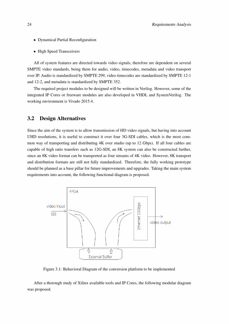
requirements into account, the following functional diagram is proposed.
Figure 3.1: Behavioral Diagram of the conversion platform to be implemented
After a thorough study of Xilinx available tools and IP Cores, the following modular diagram
was proposed.
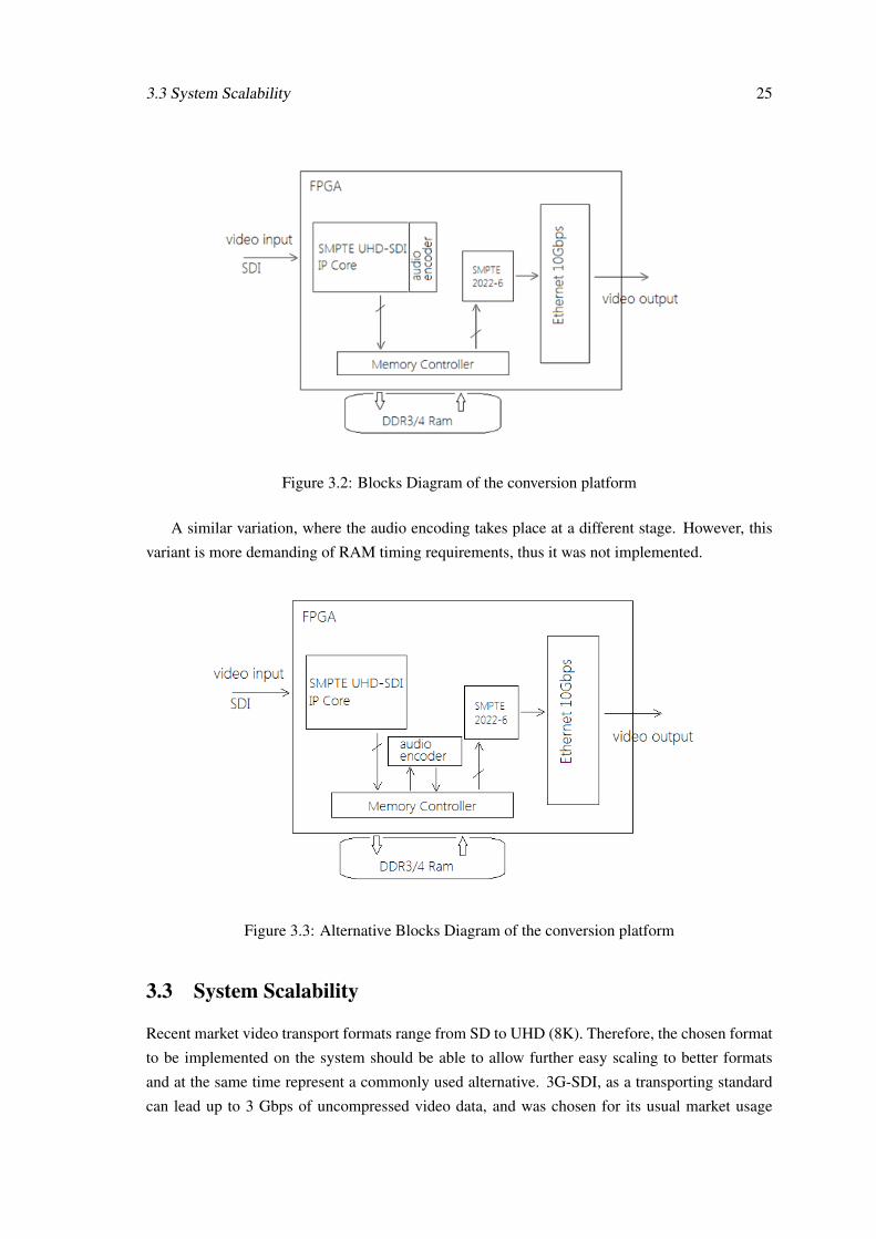
3.3 System Scalability 25
Figure 3.2: Blocks Diagram of the conversion platform
A similar variation, where the audio encoding takes place at a different stage. However, this
variant is more demanding of RAM timing requirements, thus it was not implemented.
Figure 3.3: Alternative Blocks Diagram of the conversion platform
3.3 System Scalability
Recent market video transport formats range from SD to UHD (8K). Therefore, the chosen format
to be implemented on the system should be able to allow further easy scaling to better formats
and at the same time represent a commonly used alternative. 3G-SDI, as a transporting standard
can lead up to 3 Gbps of uncompressed video data, and was chosen for its usual market usage
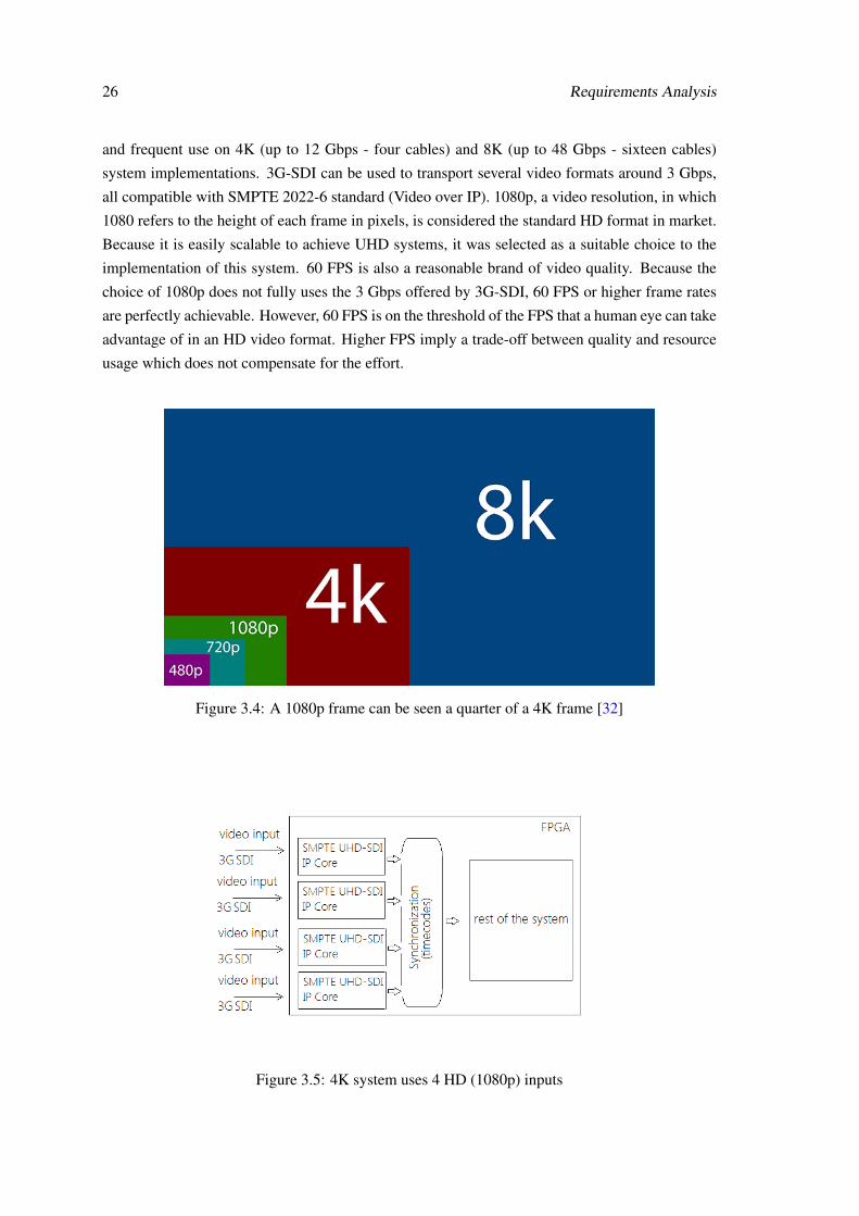
26 Requirements Analysis
and frequent use on 4K (up to 12 Gbps - four cables) and 8K (up to 48 Gbps - sixteen cables)
system implementations. 3G-SDI can be used to transport several video formats around 3 Gbps,
all compatible with SMPTE 2022-6 standard (Video over IP). 1080p, a video resolution, in which
1080 refers to the height of each frame in pixels, is considered the standard HD format in market.
Because it is easily scalable to achieve UHD systems, it was selected as a suitable choice to the
implementation of this system. 60 FPS is also a reasonable brand of video quality. Because the
choice of 1080p does not fully uses the 3 Gbps offered by 3G-SDI, 60 FPS or higher frame rates
are perfectly achievable. However, 60 FPS is on the threshold of the FPS that a human eye can take
advantage of in an HD video format. Higher FPS imply a trade-off between quality and resource
usage which does not compensate for the effort.
Figure 3.4: A 1080p frame can be seen a quarter of a 4K frame [32]
Figure 3.5: 4K system uses 4 HD (1080p) inputs
3.4 Project Constraints 27
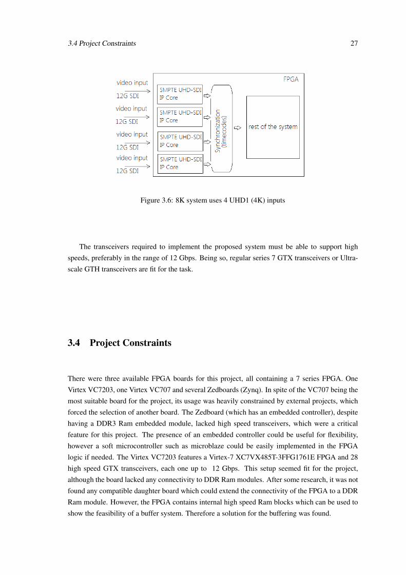
Figure 3.6: 8K system uses 4 UHD1 (4K) inputs
The transceivers required to implement the proposed system must be able to support high
speeds, preferably in the range of 12 Gbps. Being so, regular series 7 GTX transceivers or Ultra-
scale GTH transceivers are fit for the task.
3.4 Project Constraints
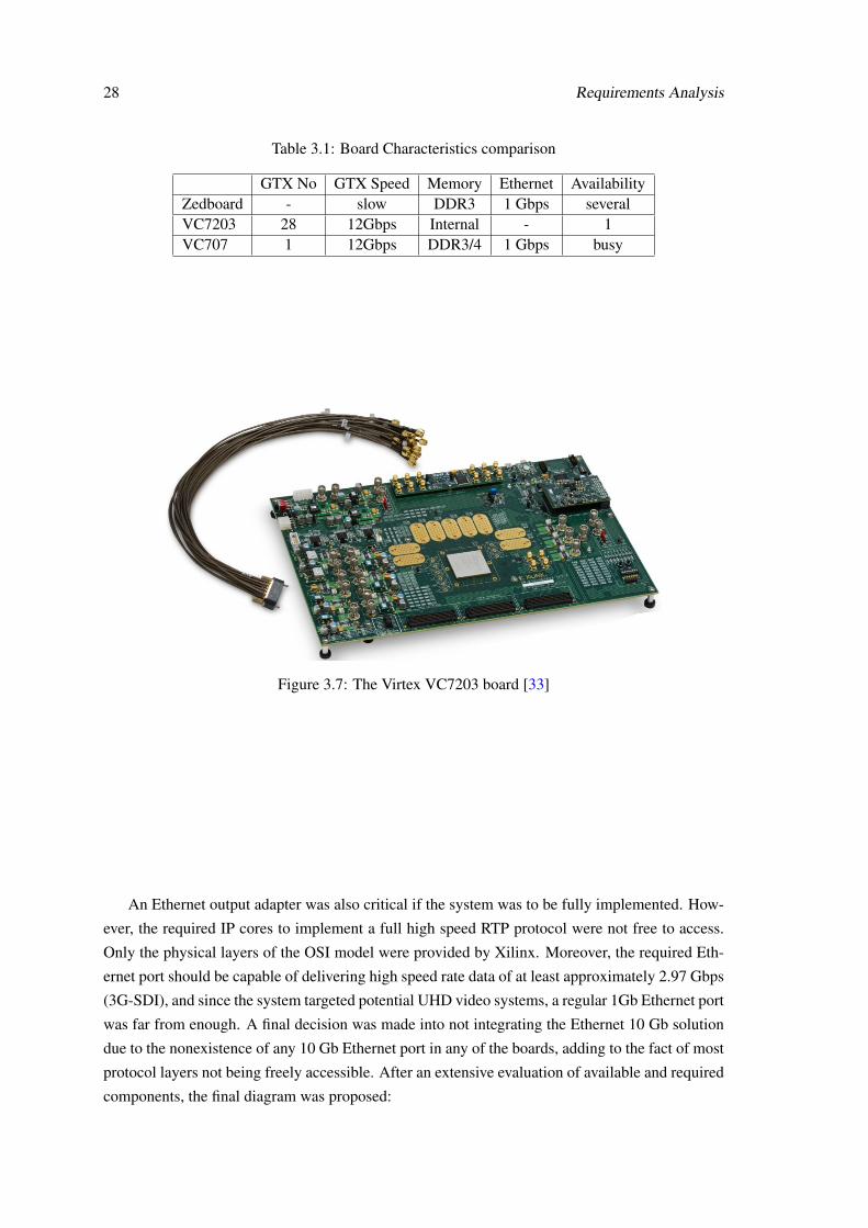
There were three available FPGA boards for this project, all containing a 7 series FPGA. One
Virtex VC7203, one Virtex VC707 and several Zedboards (Zynq). In spite of the VC707 being the
most suitable board for the project, its usage was heavily constrained by external projects, which
forced the selection of another board. The Zedboard (which has an embedded controller), despite
having a DDR3 Ram embedded module, lacked high speed transceivers, which were a critical
feature for this project. The presence of an embedded controller could be useful for flexibility,
however a soft microcontroller such as microblaze could be easily implemented in the FPGA
logic if needed. The Virtex VC7203 features a Virtex-7 XC7VX485T-3FFG1761E FPGA and 28
high speed GTX transceivers, each one up to 12 Gbps. This setup seemed fit for the project,
although the board lacked any connectivity to DDR Ram modules. After some research, it was not
found any compatible daughter board which could extend the connectivity of the FPGA to a DDR
Ram module. However, the FPGA contains internal high speed Ram blocks which can be used to
show the feasibility of a buffer system. Therefore a solution for the buffering was found.
28 Requirements Analysis
Table 3.1: Board Characteristics comparison
GTX No GTX Speed Memory Ethernet AvailabilityZedboard - slow DDR3 1 Gbps severalVC7203 28 12Gbps Internal - 1VC707 1 12Gbps DDR3/4 1 Gbps busy
Figure 3.7: The Virtex VC7203 board [33]
An Ethernet output adapter was also critical if the system was to be fully implemented. How-
ever, the required IP cores to implement a full high speed RTP protocol were not free to access.
Only the physical layers of the OSI model were provided by Xilinx. Moreover, the required Eth-
ernet port should be capable of delivering high speed rate data of at least approximately 2.97 Gbps
(3G-SDI), and since the system targeted potential UHD video systems, a regular 1Gb Ethernet port
was far from enough. A final decision was made into not integrating the Ethernet 10 Gb solution
due to the nonexistence of any 10 Gb Ethernet port in any of the boards, adding to the fact of most
protocol layers not being freely accessible. After an extensive evaluation of available and required
components, the final diagram was proposed:
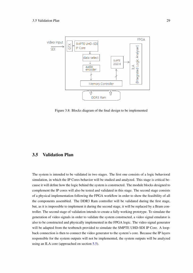
3.5 Validation Plan 29
Figure 3.8: Blocks diagram of the final design to be implemented
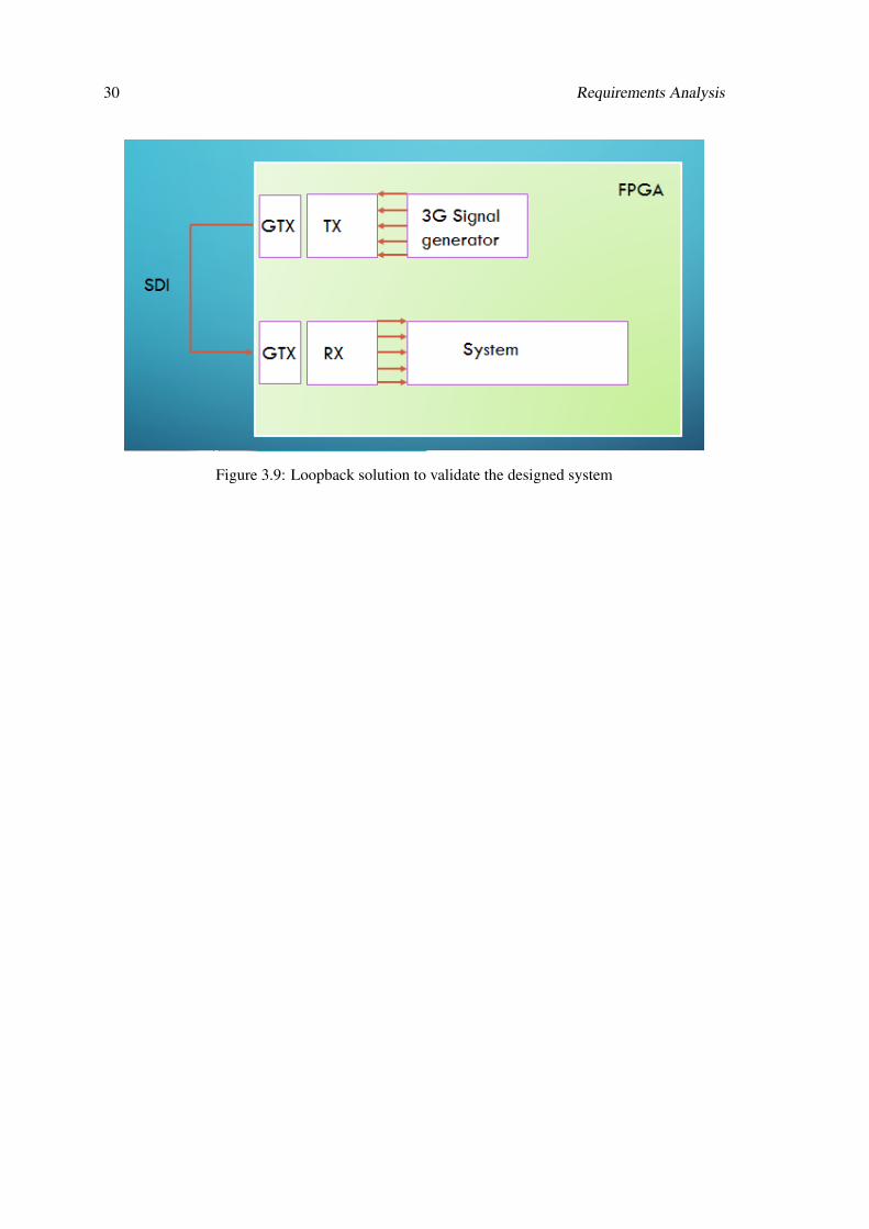
3.5 Validation Plan
The system is intended to be validated in two stages. The first one consists of a logic behavioral
simulation, in which the IP Cores behavior will be studied and analyzed. This stage is critical be-
cause it will define how the logic behind the system is constructed. The module blocks designed to
complement the IP cores will also be tested and validated in this stage. The second stage consists
of a physical implementation following the FPGA workflow in order to show the feasibility of all
the components assembled. The DDR3 Ram controller will be validated during the first stage,
but, as it is impossible to implement it during the second stage, it will be replaced by a Bram con-
troller. The second stage of validation intends to create a fully working prototype. To simulate the
generation of video signals in order to validate the system constructed, a video signal emulator is
also to be constructed and physically implemented in the FPGA logic. The video signal generator
will be adapted from the testbench provided to simulate the SMPTE UHD-SDI IP Core. A loop-
back connection is then to connect the video generator to the system’s core. Because the IP layers
responsible for the system outputs will not be implemented, the system outputs will be analyzed
using an ILA core (approached on section 5.5).
30 Requirements Analysis
Figure 3.9: Loopback solution to validate the designed system
Chapter 4
Implementation
The present chapter refers to the implementation stage, where the proposed system on the previous
chapter was designed and simulated in Vivado environment. This chapter gives a technical insight
on how the assembled IP Cores and modules work and about the algorithms applied. Several
alternate approaches are also occasionally mentioned and globally explained.
4.1 The SMPTE UHD-SDI IP Core - Simulation
The SMPTE UHD-SDI IP Core is a dedicated solution, built to allow compatibility between SDI
video transporting standards and FPGA logic. It receives parallel data through the GTX or GTH
transceivers and deserializes the video stream into multiple channels, alongside other ancillary
signals, allowing for easy user usage and parallel processing. The SMPTE UHD-SDI User Inter-
face is made of a vast range of signals, which can be divided between a reception and a transmitter
module. After an extensive analysis about these IP core signals, the core was simulated using the
testbench provided. The testbench is composed of one main test case controlling two test modules
– a Master and a Slave. The Master behaves as a signal generator supporting the generation of sev-
eral video formats and ratios. The system’s body is connected as a loopback, directly connecting
the Transmitter to the Receiver, emulating a real deserialization and subsequent serialization of
video streams. The slave receives information from the master, stating the format, ratio and meta-
data being generated. The slave module then checks if the Transmitter and Receiver are working
properly, by checking if the received data matches the transmitted. It is the Slave module which
commands the testbench to stop after a user defined number of video lines have been simulated.
31
32 Implementation
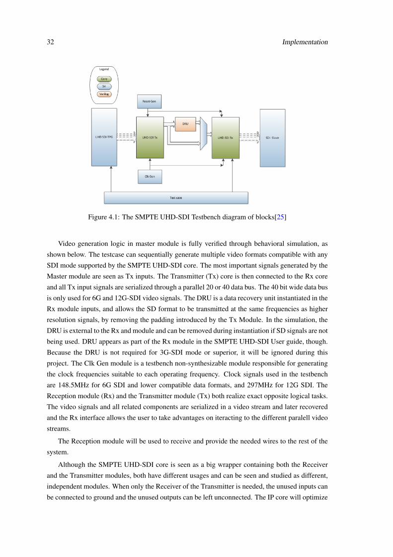
Figure 4.1: The SMPTE UHD-SDI Testbench diagram of blocks[25]
Video generation logic in master module is fully verified through behavioral simulation, as
shown below. The testcase can sequentially generate multiple video formats compatible with any
SDI mode supported by the SMPTE UHD-SDI core. The most important signals generated by the
Master module are seen as Tx inputs. The Transmitter (Tx) core is then connected to the Rx core
and all Tx input signals are serialized through a parallel 20 or 40 data bus. The 40 bit wide data bus
is only used for 6G and 12G-SDI video signals. The DRU is a data recovery unit instantiated in the
Rx module inputs, and allows the SD format to be transmitted at the same frequencies as higher
resolution signals, by removing the padding introduced by the Tx Module. In the simulation, the
DRU is external to the Rx and module and can be removed during instantiation if SD signals are not
being used. DRU appears as part of the Rx module in the SMPTE UHD-SDI User guide, though.
Because the DRU is not required for 3G-SDI mode or superior, it will be ignored during this
project. The Clk Gen module is a testbench non-synthesizable module responsible for generating
the clock frequencies suitable to each operating frequency. Clock signals used in the testbench
are 148.5MHz for 6G SDI and lower compatible data formats, and 297MHz for 12G SDI. The
Reception module (Rx) and the Transmitter module (Tx) both realize exact opposite logical tasks.
The video signals and all related components are serialized in a video stream and later recovered
and the Rx interface allows the user to take advantages on iteracting to the different paralell video
streams.
The Reception module will be used to receive and provide the needed wires to the rest of the
system.
Although the SMPTE UHD-SDI core is seen as a big wrapper containing both the Receiver
and the Transmitter modules, both have different usages and can be seen and studied as different,
independent modules. When only the Receiver of the Transmitter is needed, the unused inputs can
be connected to ground and the unused outputs can be left unconnected. The IP core will optimize
4.1 The SMPTE UHD-SDI IP Core - Simulation 33
Table 4.1: SMPTE UHD-SDI Signals - Transmission
Tx signalstx_ce_in Clock enable input. It must be high to enable the system to work.
tx_mode_inInput port to select which SDI mode is selected for the transmitter.010 for 3G-SDI
tx_insert_crc When high, the transmitter generates and inserts CRC to every video lines.tx_insert_ln When high, the transmitter inserts line numbers to every video line.
tx_insert_st352When high, the transmitter inserts ST352 packets to video.ST352 packets correspond to video metadata.
tx_line_0_in totx_line_7_in
Current video line number for each stream pair.It is inserted everytime tx_insert_ln is asserted.
tx_ds1_in Data stream input 1. Corresponds to Y’ Channel in 3G SDI A mode.tx_ds2_in Data stream input 2. Corresponds to Cb’Cr’ channel in 3G SDI A mode.tx_ds3_in totx_ds16_in
Remaining data stream inputs. Not used in 3G SDI A mode.
Table 4.2: SMPTE UHD-SDI Signals - Reception
Rx signalsrx_mode_en_in Enables which modules are supported by the receiver interface.rx_mode_detect_en_in When high, this signal enables SDI mode detection.
rx_mode_outThis signal indicates which SDI mode was detected.010 for 3G-SDI
rx_t_locked_out This signal is asserted HIGH when the Rx core detects the SDI mode.rx_active_streams_out This port indicates the number of data streams that are active.rx_line_0_out torx_line_7_out
This ports contain the recovered line numbers for each pair of stream channels.
rx_ds1_out Data stream output 1. Corresponds to Y’ Channel in 3G SDI A mode.rx_ds2_out Data stream output 2. Corresponds to Cb’Cr’ Channel in 3G SDI A mode.rx_ds3_out to torx_ds16_out
Remaining data stream inputs. Not used in 3G SDI A mode.
rx_eav_out High when the XYZ word of an EAV is present.rx_sav_out High when the XYZ word of an SAV is present.rx_trs_out High when the 4 consecutive words of any EAV or SAV are present.
34 Implementation
the resource usage.
Figure 4.2: Usage example for the Rx and Tx modules inside the SMPTE UHD-SDI
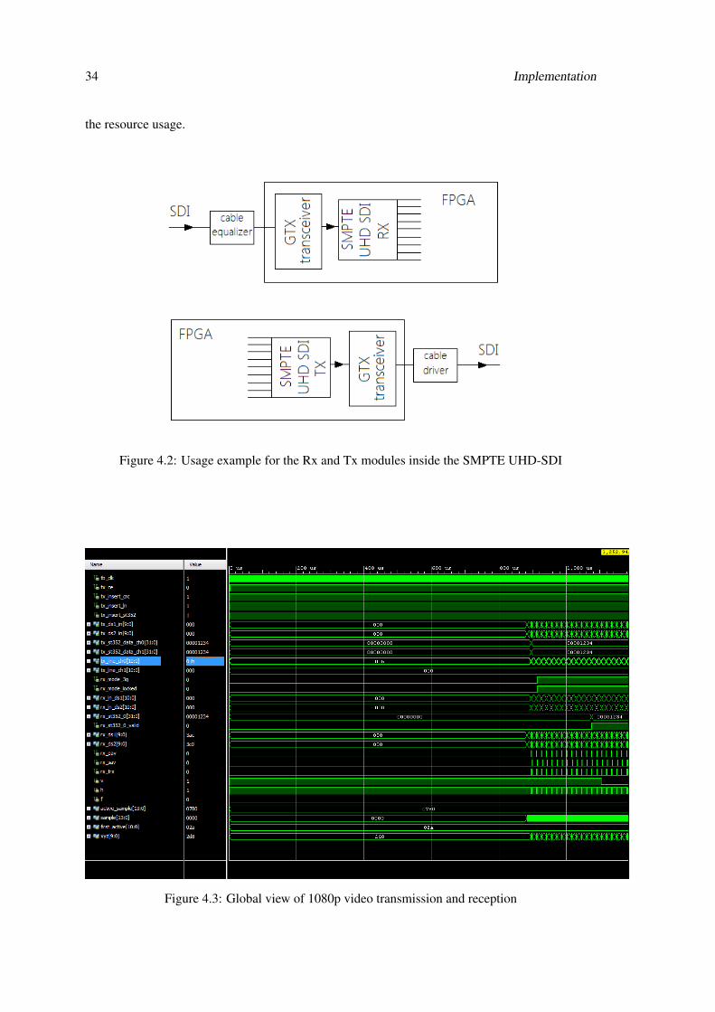
Figure 4.3: Global view of 1080p video transmission and reception
4.1 The SMPTE UHD-SDI IP Core - Simulation 35
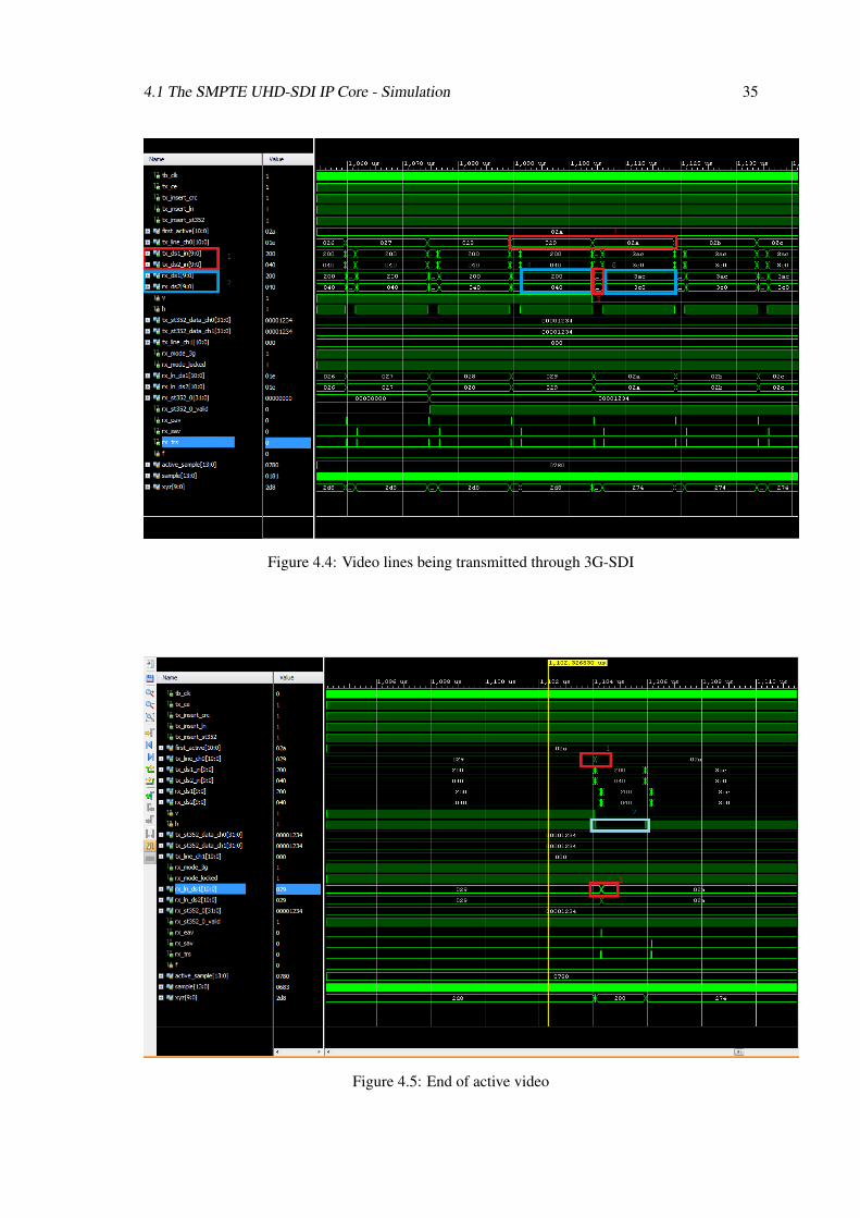
Figure 4.4: Video lines being transmitted through 3G-SDI
Figure 4.5: End of active video
36 Implementation
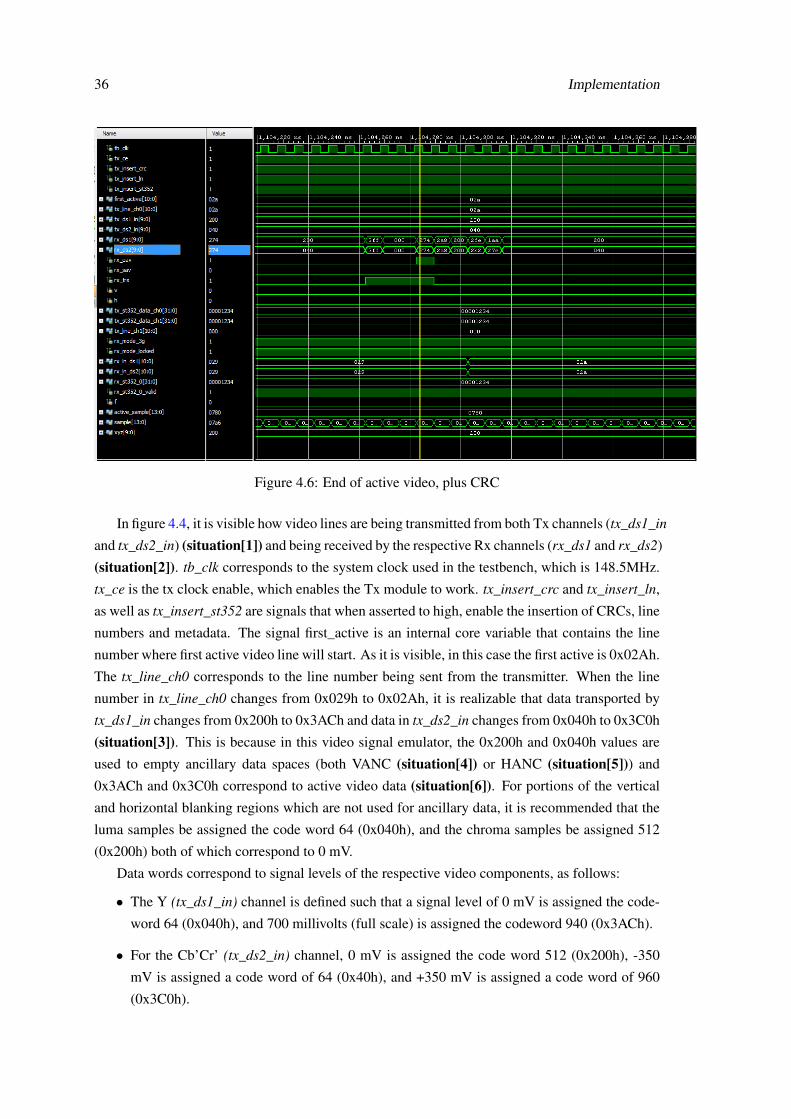
Figure 4.6: End of active video, plus CRC
In figure 4.4, it is visible how video lines are being transmitted from both Tx channels (tx_ds1_in
and tx_ds2_in) (situation[1]) and being received by the respective Rx channels (rx_ds1 and rx_ds2)
(situation[2]). tb_clk corresponds to the system clock used in the testbench, which is 148.5MHz.
tx_ce is the tx clock enable, which enables the Tx module to work. tx_insert_crc and tx_insert_ln,
as well as tx_insert_st352 are signals that when asserted to high, enable the insertion of CRCs, line
numbers and metadata. The signal first_active is an internal core variable that contains the line
number where first active video line will start. As it is visible, in this case the first active is 0x02Ah.
The tx_line_ch0 corresponds to the line number being sent from the transmitter. When the line
number in tx_line_ch0 changes from 0x029h to 0x02Ah, it is realizable that data transported by
tx_ds1_in changes from 0x200h to 0x3ACh and data in tx_ds2_in changes from 0x040h to 0x3C0h
(situation[3]). This is because in this video signal emulator, the 0x200h and 0x040h values are
used to empty ancillary data spaces (both VANC (situation[4]) or HANC (situation[5])) and
0x3ACh and 0x3C0h correspond to active video data (situation[6]). For portions of the vertical
and horizontal blanking regions which are not used for ancillary data, it is recommended that the
luma samples be assigned the code word 64 (0x040h), and the chroma samples be assigned 512
(0x200h) both of which correspond to 0 mV.
Data words correspond to signal levels of the respective video components, as follows:
• The Y (tx_ds1_in) channel is defined such that a signal level of 0 mV is assigned the code-
word 64 (0x040h), and 700 millivolts (full scale) is assigned the codeword 940 (0x3ACh).
• For the Cb’Cr’ (tx_ds2_in) channel, 0 mV is assigned the code word 512 (0x200h), -350
mV is assigned a code word of 64 (0x40h), and +350 mV is assigned a code word of 960
(0x3C0h).
4.2 Audio Encoding 37
Inside tx_ds1_in and tx_ds2_in channels, some video patterns are perceivable. The 0x200h
and 0x040h values as well as the 0x3ACh and 0x3C0h values are followed up by some small
intervals of data. This is easily explained by the h signal below. The h signals the Horizontal
ancillary data space (HANC). When h is asserted to high, it means that the next termination flags
will be EAV. Therefore, h is high during active video and low during HANC. v signal is used to
distinguish VANC from active video. It is perceivable that v goes to 0 on the change from line
0x029h to 0x02Ah. This transition is more visible in figure 4.5, situation [2].Both rx_ds1 and rx_ds2 correspond to tx_ds1_in and tx_ds2_in recovered in the Rx side, 4.5,
situation [1]. The delay introduced is perceivable in the following pictures.
tx_st352_data represents the metadata sent in both video streams 1 and 2. In this case, it is
dummy, as one can see the values being sent were 1234 in both streams. rx_mode_3G is asserted to
high because 3G mode was detected. rx_mode_locked was asserted to high because the Receptor
Rx locked in some video SDI format, in this case 3G, as stated. The rx_ln_ds1 and rx_ln_ds2
correspond to video lines recovered in Rx, which correspond to the ones in tx_line_ch0 with some
delay. rx_st352_0 corresponds to the recovered metadata in the reception Rx side. As one can
see, only after the end of VANC, the metadata is delivered. The rx_st352_0_valid rises to high
as metadata was recovered. rx_eav, rx_sav are asserted to high when EAV or SAV are reached.
It is clear as they are risen every time rx_ds1 and rx_ds2 switch values. rx_trs is high when
either rx_sav or rx_eav are asserted to high. f signal at low corresponds to progressive video, as
expected, whilst high corresponds to interlaced. f, v and h are combined to achieve the XYZ value.
XYZ = {1’b1, f, v, h, vˆ h ,fˆ h, fˆ v, fˆ vˆ h, 2’b00};
This value is present during every SAV and EAV and allows for error control. The active sample
value is 0x780h, which in decimal stands for 1920, the total number of line pixels that a 1080p
frame has. sample is an internal variable that corresponds to the sample number of each value
acquired from rs_ds1 and rx_ds2. It changes in every clock, and corresponds to the pixel counter
for each video line.
Figure 4.6 corresponds to a detailed view of EAV. When rs_ds1 and rs_ds2 receive the se-
quence 0x3FFh, 0x000h, 0x000h and 0xYXZh (0x274h), the flag EAV is asserted to high. rx_trs
is asserted high in the beginning of every Timing Reference Signals (both EAV and SAV).
4.2 Audio Encoding
The compressing μ-law and a-law modules were gathered as Free Ip Cores on the Internet, al-
though its use is restricted. The first approach was to validate both a-law and μ-law modules. For
this, a logical simulation was executed, aiming to show how, for any valid input, both encoders
would provide a correct output. The encoded outputs were then subjected to a recovery to the
original audio format and both the original data and the reconverted audio were compared. To test
every possible 13 bit input values, a 13 bit counter was generated, starting in 0 and incrementing
synchronously with the system clock signal. For each value generated by the counter, a converted
corresponding 8 bits output was generated and stored in a .txt file. Since the input supported by
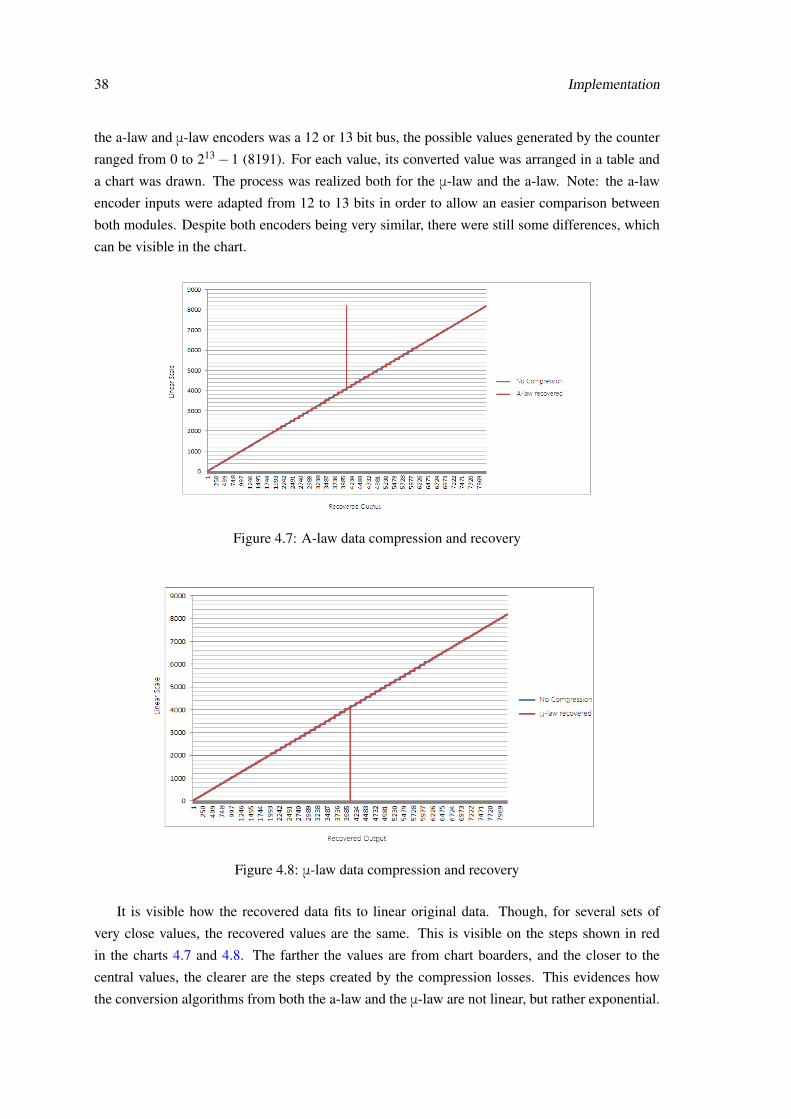
38 Implementation
the a-law and μ-law encoders was a 12 or 13 bit bus, the possible values generated by the counter
ranged from 0 to 213− 1 (8191). For each value, its converted value was arranged in a table and
a chart was drawn. The process was realized both for the μ-law and the a-law. Note: the a-law
encoder inputs were adapted from 12 to 13 bits in order to allow an easier comparison between
both modules. Despite both encoders being very similar, there were still some differences, which
can be visible in the chart.
Figure 4.7: A-law data compression and recovery
Figure 4.8: μ-law data compression and recovery
It is visible how the recovered data fits to linear original data. Though, for several sets of
very close values, the recovered values are the same. This is visible on the steps shown in red
in the charts 4.7 and 4.8. The farther the values are from chart boarders, and the closer to the
central values, the clearer are the steps created by the compression losses. This evidences how
the conversion algorithms from both the a-law and the μ-law are not linear, but rather exponential.
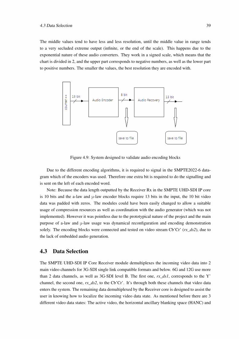
4.3 Data Selection 39
The middle values tend to have less and less resolution, until the middle value in range tends
to a very secluded extreme output (infinite, or the end of the scale). This happens due to the
exponential nature of these audio converters. They work in a signed scale, which means that the
chart is divided in 2, and the upper part corresponds to negative numbers, as well as the lower part
to positive numbers. The smaller the values, the best resolution they are encoded with.
Figure 4.9: System designed to validate audio encoding blocks
Due to the different encoding algorithms, it is required to signal in the SMPTE2022-6 data-
gram which of the encoders was used. Therefore one extra bit is required to do the signalling and
is sent on the left of each encoded word.
Note: Because the data length outputted by the Receiver Rx in the SMPTE UHD-SDI IP core
is 10 bits and the a-law and μ-law encoder blocks require 13 bits in the input, the 10 bit video
data was padded with zeros. The modules could have been easily changed to allow a suitable
usage of compression resources as well as coordination with the audio generator (which was not
implemented). However it was pointless due to the prototypical nature of the project and the main
purpose of a-law and μ-law usage was dynamical reconfiguration and encoding demonstration
solely. The encoding blocks were connected and tested on video stream Cb’Cr’ (rx_ds2), due to
the lack of embedded audio generation.
4.3 Data Selection
The SMPTE UHD-SDI IP Core Receiver module demultiplexes the incoming video data into 2
main video channels for 3G-SDI single link compatible formats and below. 6G and 12G use more
than 2 data channels, as well as 3G-SDI level B. The first one, rx_ds1, corresponds to the Y’
channel, the second one, rx_ds2, to the Cb’Cr’. It’s through both these channels that video data
enters the system. The remaining data demultiplexed by the Receiver core is designed to assist the
user in knowing how to localize the incoming video data state. As mentioned before there are 3
different video data states: The active video, the horizontal ancillary blanking space (HANC) and
40 Implementation
the vertical ancillary blanking space. The active video is where pixel information related to video
frames is transported (Y’Cb’Cr’). The HANC is where most ancillary data is transported. The
HANC space is present every time after an Y’Cb’Cr’ line is finished. There are termination flags,
line numbers and CRC delimiting the space between video active zones and HANC zones. The
VANC is present only when desired. Typically VANC is used to transport other kind of ancillary
data, like teletex. In opposition to HANC, which is present in every video line, when VANC
is present, video information ceases to be transmitted. VANC can work as video suppression if
needed, however without interrupting the video stream connection. VANC can also be used to give
time to video receptors while they synchronize and recover clock frequency, without losing actual
video data. This is a possible application on dynamic partial reconfiguration. During the time the
system reconfigures, video is suppressed and VANC gives time to the encoder block to change.
This will be explored further. There are signals responsible for indicating from which of HANC,
VANC or Active Video, some piece of data is from. When v is one, VANC is active, when h is 0,
HANC is active. When h is 1 and v is 0, Active picture is active.
The data targeted for recovery and worked with in this application is composed of:
• video frames
• audio
• timecodes
• metadata (Payload ID)
A data selection core is required to be placed right after the SMPTE UHD-SDI Receiver mod-
ule, in order to identify and allow further modules to know with what data they are dealing with.
This core can be seen as an auxiliary module to complement the SMPTE UHD-SDI IP core.
The detection of different types of video data must be done by analyzing the 2 video channels
outputted by the Reception module, and following the SMPTE standards.
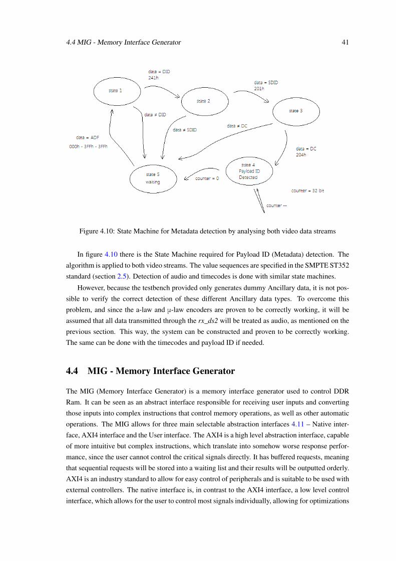
4.4 MIG - Memory Interface Generator 41
Figure 4.10: State Machine for Metadata detection by analysing both video data streams
In figure 4.10 there is the State Machine required for Payload ID (Metadata) detection. The
algorithm is applied to both video streams. The value sequences are specified in the SMPTE ST352
standard (section 2.5). Detection of audio and timecodes is done with similar state machines.
However, because the testbench provided only generates dummy Ancillary data, it is not pos-
sible to verify the correct detection of these different Ancillary data types. To overcome this
problem, and since the a-law and μ-law encoders are proven to be correctly working, it will be
assumed that all data transmitted through the rx_ds2 will be treated as audio, as mentioned on the
previous section. This way, the system can be constructed and proven to be correctly working.
The same can be done with the timecodes and payload ID if needed.
4.4 MIG - Memory Interface Generator
The MIG (Memory Interface Generator) is a memory interface generator used to control DDR
Ram. It can be seen as an abstract interface responsible for receiving user inputs and converting
those inputs into complex instructions that control memory operations, as well as other automatic
operations. The MIG allows for three main selectable abstraction interfaces 4.11 – Native inter-
face, AXI4 interface and the User interface. The AXI4 is a high level abstraction interface, capable
of more intuitive but complex instructions, which translate into somehow worse response perfor-
mance, since the user cannot control the critical signals directly. It has buffered requests, meaning
that sequential requests will be stored into a waiting list and their results will be outputted orderly.
AXI4 is an industry standard to allow for easy control of peripherals and is suitable to be used with
external controllers. The native interface is, in contrast to the AXI4 interface, a low level control
interface, which allows for the user to control most signals individually, allowing for optimizations
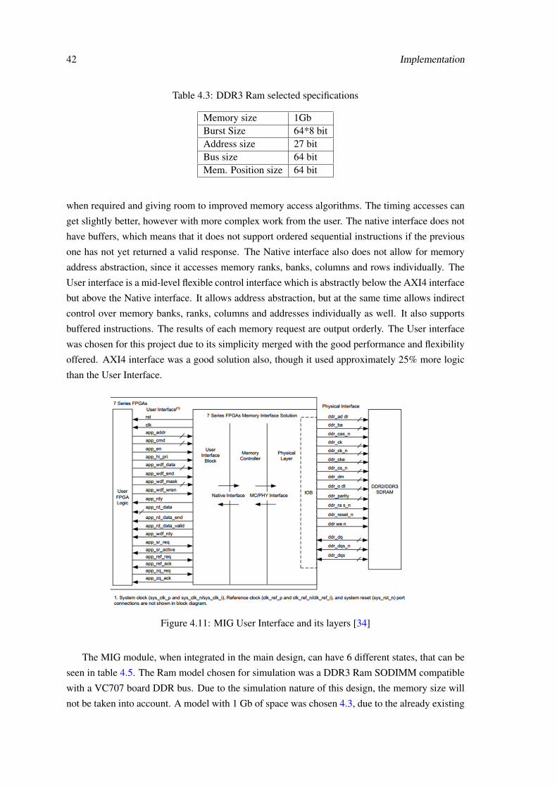
42 Implementation
Table 4.3: DDR3 Ram selected specifications
Memory size 1GbBurst Size 64*8 bitAddress size 27 bitBus size 64 bitMem. Position size 64 bit
when required and giving room to improved memory access algorithms. The timing accesses can
get slightly better, however with more complex work from the user. The native interface does not
have buffers, which means that it does not support ordered sequential instructions if the previous
one has not yet returned a valid response. The Native interface also does not allow for memory
address abstraction, since it accesses memory ranks, banks, columns and rows individually. The
User interface is a mid-level flexible control interface which is abstractly below the AXI4 interface
but above the Native interface. It allows address abstraction, but at the same time allows indirect
control over memory banks, ranks, columns and addresses individually as well. It also supports
buffered instructions. The results of each memory request are output orderly. The User interface
was chosen for this project due to its simplicity merged with the good performance and flexibility
offered. AXI4 interface was a good solution also, though it used approximately 25% more logic
than the User Interface.
Figure 4.11: MIG User Interface and its layers [34]
The MIG module, when integrated in the main design, can have 6 different states, that can be
seen in table 4.5. The Ram model chosen for simulation was a DDR3 Ram SODIMM compatible
with a VC707 board DDR bus. Due to the simulation nature of this design, the memory size will
not be taken into account. A model with 1 Gb of space was chosen 4.3, due to the already existing
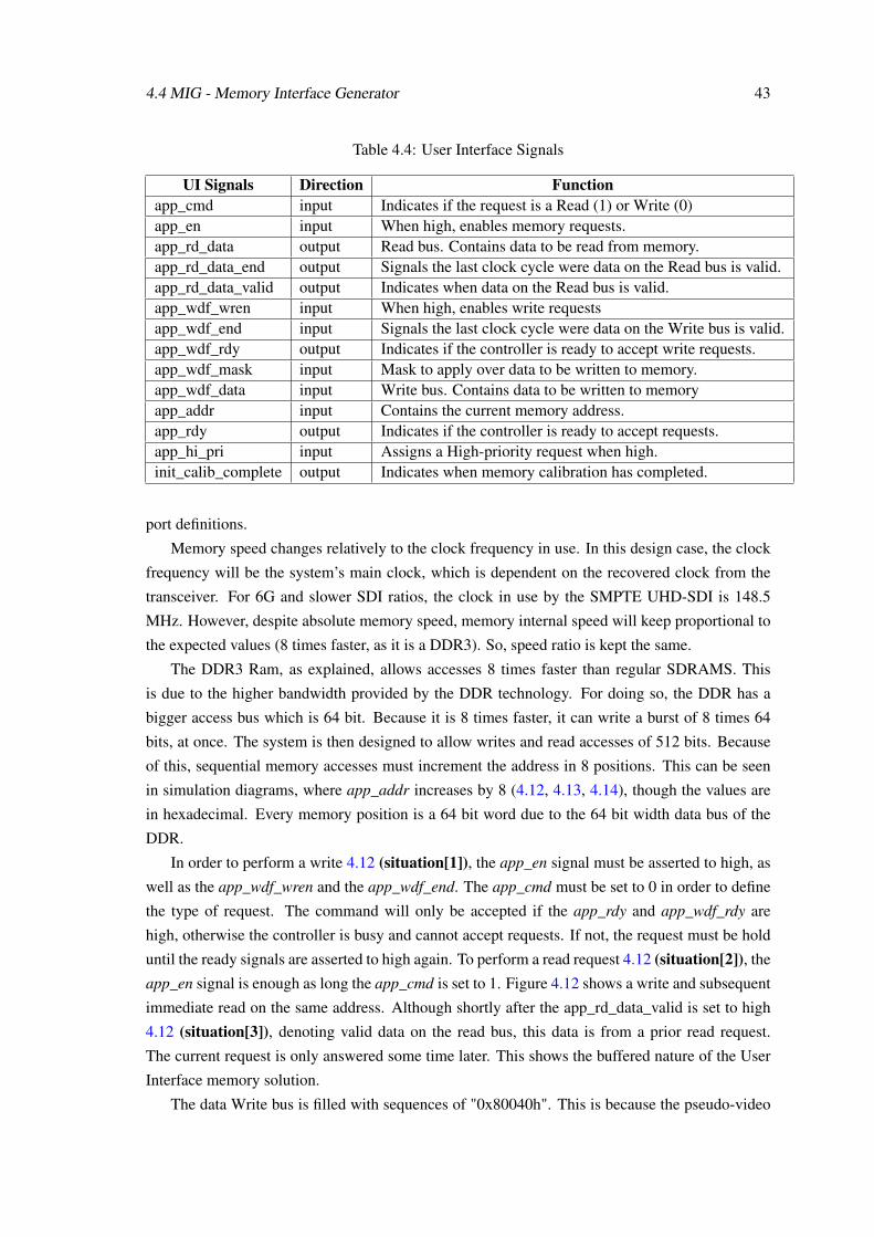
4.4 MIG - Memory Interface Generator 43
Table 4.4: User Interface Signals
UI Signals Direction Functionapp_cmd input Indicates if the request is a Read (1) or Write (0)app_en input When high, enables memory requests.app_rd_data output Read bus. Contains data to be read from memory.app_rd_data_end output Signals the last clock cycle were data on the Read bus is valid.app_rd_data_valid output Indicates when data on the Read bus is valid.app_wdf_wren input When high, enables write requestsapp_wdf_end input Signals the last clock cycle were data on the Write bus is valid.app_wdf_rdy output Indicates if the controller is ready to accept write requests.app_wdf_mask input Mask to apply over data to be written to memory.app_wdf_data input Write bus. Contains data to be written to memoryapp_addr input Contains the current memory address.app_rdy output Indicates if the controller is ready to accept requests.app_hi_pri input Assigns a High-priority request when high.init_calib_complete output Indicates when memory calibration has completed.
port definitions.
Memory speed changes relatively to the clock frequency in use. In this design case, the clock
frequency will be the system’s main clock, which is dependent on the recovered clock from the
transceiver. For 6G and slower SDI ratios, the clock in use by the SMPTE UHD-SDI is 148.5
MHz. However, despite absolute memory speed, memory internal speed will keep proportional to
the expected values (8 times faster, as it is a DDR3). So, speed ratio is kept the same.
The DDR3 Ram, as explained, allows accesses 8 times faster than regular SDRAMS. This
is due to the higher bandwidth provided by the DDR technology. For doing so, the DDR has a
bigger access bus which is 64 bit. Because it is 8 times faster, it can write a burst of 8 times 64
bits, at once. The system is then designed to allow writes and read accesses of 512 bits. Because
of this, sequential memory accesses must increment the address in 8 positions. This can be seen
in simulation diagrams, where app_addr increases by 8 (4.12, 4.13, 4.14), though the values are
in hexadecimal. Every memory position is a 64 bit word due to the 64 bit width data bus of the
DDR.
In order to perform a write 4.12 (situation[1]), the app_en signal must be asserted to high, as
well as the app_wdf_wren and the app_wdf_end. The app_cmd must be set to 0 in order to define
the type of request. The command will only be accepted if the app_rdy and app_wdf_rdy are
high, otherwise the controller is busy and cannot accept requests. If not, the request must be hold
until the ready signals are asserted to high again. To perform a read request 4.12 (situation[2]), the
app_en signal is enough as long the app_cmd is set to 1. Figure 4.12 shows a write and subsequent
immediate read on the same address. Although shortly after the app_rd_data_valid is set to high
4.12 (situation[3]), denoting valid data on the read bus, this data is from a prior read request.
The current request is only answered some time later. This shows the buffered nature of the User
Interface memory solution.
The data Write bus is filled with sequences of "0x80040h". This is because the pseudo-video
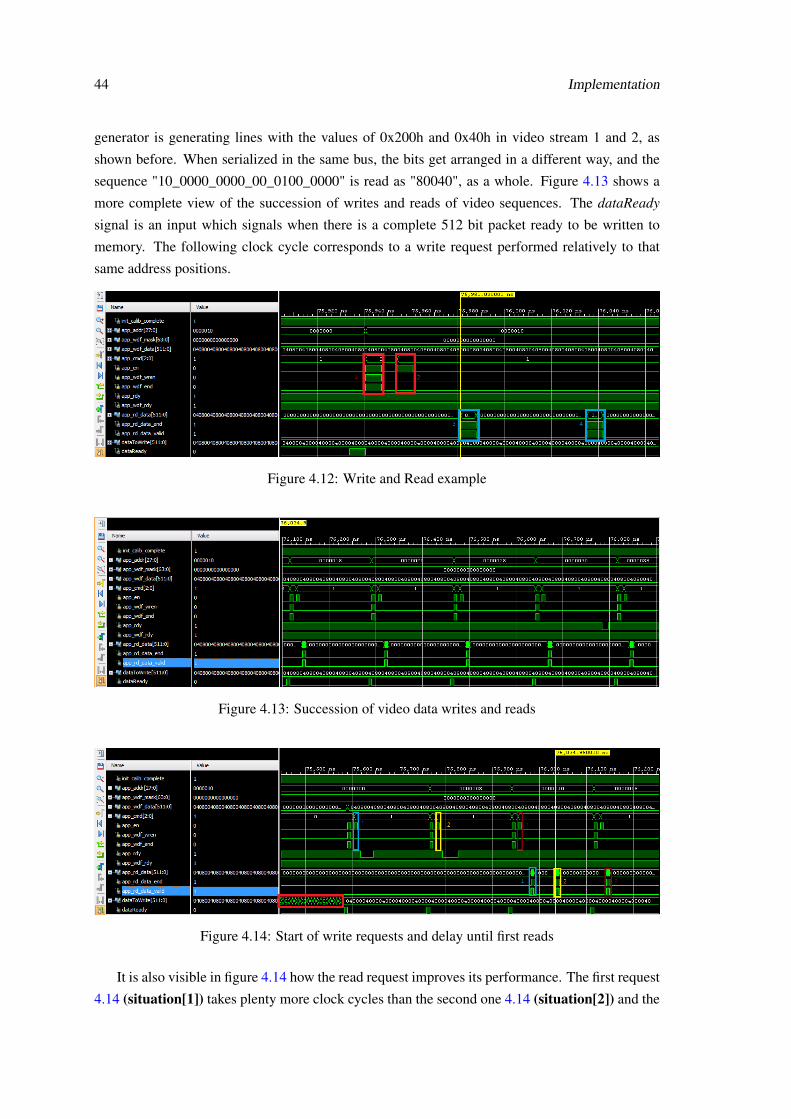
44 Implementation
generator is generating lines with the values of 0x200h and 0x40h in video stream 1 and 2, as
shown before. When serialized in the same bus, the bits get arranged in a different way, and the
sequence "10_0000_0000_00_0100_0000" is read as "80040", as a whole. Figure 4.13 shows a
more complete view of the succession of writes and reads of video sequences. The dataReady
signal is an input which signals when there is a complete 512 bit packet ready to be written to
memory. The following clock cycle corresponds to a write request performed relatively to that
same address positions.
Figure 4.12: Write and Read example
Figure 4.13: Succession of video data writes and reads
Figure 4.14: Start of write requests and delay until first reads
It is also visible in figure 4.14 how the read request improves its performance. The first request
4.14 (situation[1]) takes plenty more clock cycles than the second one 4.14 (situation[2]) and the
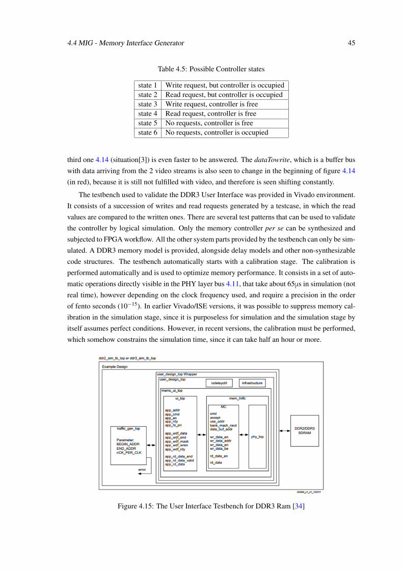
4.4 MIG - Memory Interface Generator 45
Table 4.5: Possible Controller states
state 1 Write request, but controller is occupiedstate 2 Read request, but controller is occupiedstate 3 Write request, controller is freestate 4 Read request, controller is freestate 5 No requests, controller is freestate 6 No requests, controller is occupied
third one 4.14 (situation[3]) is even faster to be answered. The dataTowrite, which is a buffer bus
with data arriving from the 2 video streams is also seen to change in the beginning of figure 4.14
(in red), because it is still not fulfilled with video, and therefore is seen shifting constantly.
The testbench used to validate the DDR3 User Interface was provided in Vivado environment.
It consists of a succession of writes and read requests generated by a testcase, in which the read
values are compared to the written ones. There are several test patterns that can be used to validate
the controller by logical simulation. Only the memory controller per se can be synthesized and
subjected to FPGA workflow. All the other system parts provided by the testbench can only be sim-
ulated. A DDR3 memory model is provided, alongside delay models and other non-synthesizable
code structures. The testbench automatically starts with a calibration stage. The calibration is
performed automatically and is used to optimize memory performance. It consists in a set of auto-
matic operations directly visible in the PHY layer bus 4.11, that take about 65μs in simulation (not
real time), however depending on the clock frequency used, and require a precision in the order
of fento seconds (10−15). In earlier Vivado/ISE versions, it was possible to suppress memory cal-
ibration in the simulation stage, since it is purposeless for simulation and the simulation stage by
itself assumes perfect conditions. However, in recent versions, the calibration must be performed,
which somehow constrains the simulation time, since it can take half an hour or more.
Figure 4.15: The User Interface Testbench for DDR3 Ram [34]
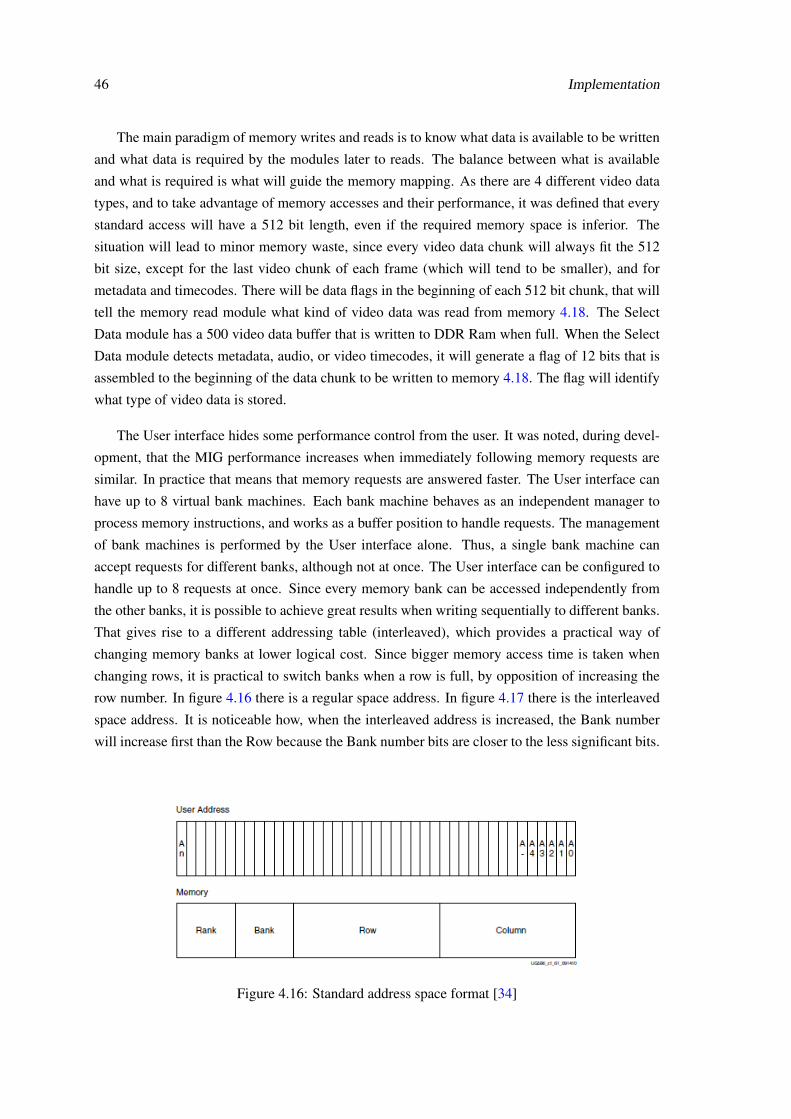
46 Implementation
The main paradigm of memory writes and reads is to know what data is available to be written
and what data is required by the modules later to reads. The balance between what is available
and what is required is what will guide the memory mapping. As there are 4 different video data
types, and to take advantage of memory accesses and their performance, it was defined that every
standard access will have a 512 bit length, even if the required memory space is inferior. The
situation will lead to minor memory waste, since every video data chunk will always fit the 512
bit size, except for the last video chunk of each frame (which will tend to be smaller), and for
metadata and timecodes. There will be data flags in the beginning of each 512 bit chunk, that will
tell the memory read module what kind of video data was read from memory 4.18. The Select
Data module has a 500 video data buffer that is written to DDR Ram when full. When the Select
Data module detects metadata, audio, or video timecodes, it will generate a flag of 12 bits that is
assembled to the beginning of the data chunk to be written to memory 4.18. The flag will identify
what type of video data is stored.
The User interface hides some performance control from the user. It was noted, during devel-
opment, that the MIG performance increases when immediately following memory requests are
similar. In practice that means that memory requests are answered faster. The User interface can
have up to 8 virtual bank machines. Each bank machine behaves as an independent manager to
process memory instructions, and works as a buffer position to handle requests. The management
of bank machines is performed by the User interface alone. Thus, a single bank machine can
accept requests for different banks, although not at once. The User interface can be configured to
handle up to 8 requests at once. Since every memory bank can be accessed independently from
the other banks, it is possible to achieve great results when writing sequentially to different banks.
That gives rise to a different addressing table (interleaved), which provides a practical way of
changing memory banks at lower logical cost. Since bigger memory access time is taken when
changing rows, it is practical to switch banks when a row is full, by opposition of increasing the
row number. In figure 4.16 there is a regular space address. In figure 4.17 there is the interleaved
space address. It is noticeable how, when the interleaved address is increased, the Bank number
will increase first than the Row because the Bank number bits are closer to the less significant bits.
Figure 4.16: Standard address space format [34]
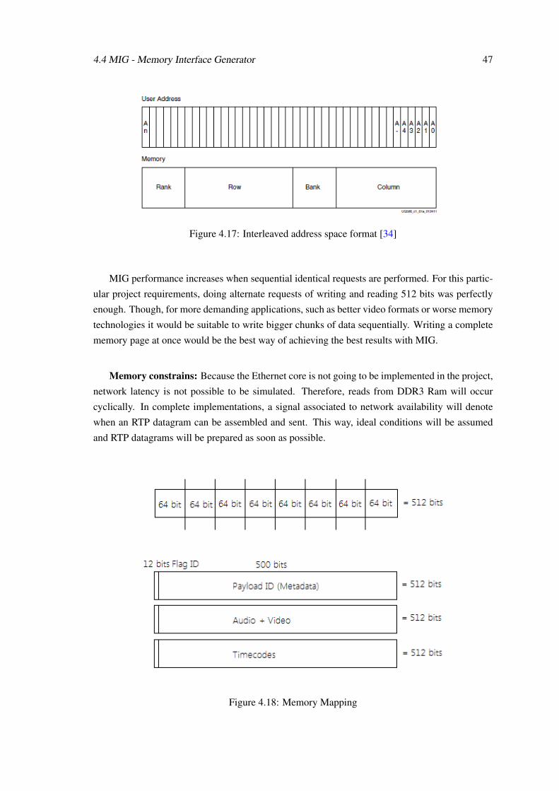
4.4 MIG - Memory Interface Generator 47
Figure 4.17: Interleaved address space format [34]
MIG performance increases when sequential identical requests are performed. For this partic-
ular project requirements, doing alternate requests of writing and reading 512 bits was perfectly
enough. Though, for more demanding applications, such as better video formats or worse memory
technologies it would be suitable to write bigger chunks of data sequentially. Writing a complete
memory page at once would be the best way of achieving the best results with MIG.
Memory constrains: Because the Ethernet core is not going to be implemented in the project,
network latency is not possible to be simulated. Therefore, reads from DDR3 Ram will occur
cyclically. In complete implementations, a signal associated to network availability will denote
when an RTP datagram can be assembled and sent. This way, ideal conditions will be assumed
and RTP datagrams will be prepared as soon as possible.
Figure 4.18: Memory Mapping
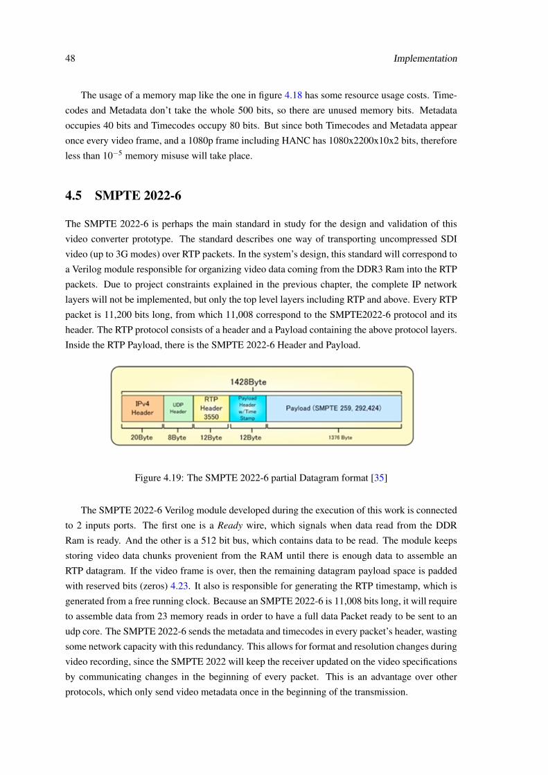
48 Implementation
The usage of a memory map like the one in figure 4.18 has some resource usage costs. Time-
codes and Metadata don’t take the whole 500 bits, so there are unused memory bits. Metadata
occupies 40 bits and Timecodes occupy 80 bits. But since both Timecodes and Metadata appear
once every video frame, and a 1080p frame including HANC has 1080x2200x10x2 bits, therefore
less than 10−5 memory misuse will take place.
4.5 SMPTE 2022-6
The SMPTE 2022-6 is perhaps the main standard in study for the design and validation of this
video converter prototype. The standard describes one way of transporting uncompressed SDI
video (up to 3G modes) over RTP packets. In the system’s design, this standard will correspond to
a Verilog module responsible for organizing video data coming from the DDR3 Ram into the RTP
packets. Due to project constraints explained in the previous chapter, the complete IP network
layers will not be implemented, but only the top level layers including RTP and above. Every RTP
packet is 11,200 bits long, from which 11,008 correspond to the SMPTE2022-6 protocol and its
header. The RTP protocol consists of a header and a Payload containing the above protocol layers.
Inside the RTP Payload, there is the SMPTE 2022-6 Header and Payload.
Figure 4.19: The SMPTE 2022-6 partial Datagram format [35]
The SMPTE 2022-6 Verilog module developed during the execution of this work is connected
to 2 inputs ports. The first one is a Ready wire, which signals when data read from the DDR
Ram is ready. And the other is a 512 bit bus, which contains data to be read. The module keeps
storing video data chunks provenient from the RAM until there is enough data to assemble an
RTP datagram. If the video frame is over, then the remaining datagram payload space is padded
with reserved bits (zeros) 4.23. It also is responsible for generating the RTP timestamp, which is
generated from a free running clock. Because an SMPTE 2022-6 is 11,008 bits long, it will require
to assemble data from 23 memory reads in order to have a full data Packet ready to be sent to an
udp core. The SMPTE 2022-6 sends the metadata and timecodes in every packet’s header, wasting
some network capacity with this redundancy. This allows for format and resolution changes during
video recording, since the SMPTE 2022 will keep the receiver updated on the video specifications
by communicating changes in the beginning of every packet. This is an advantage over other
protocols, which only send video metadata once in the beginning of the transmission.
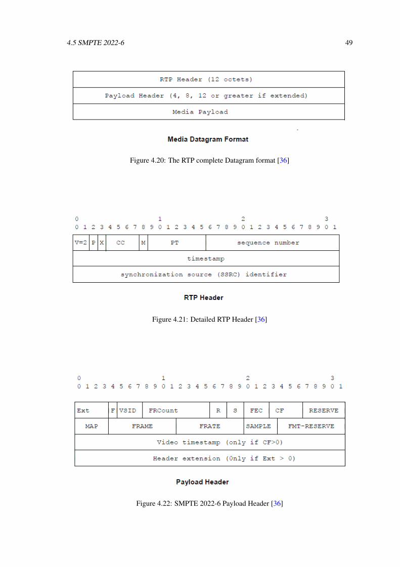
4.5 SMPTE 2022-6 49
Figure 4.20: The RTP complete Datagram format [36]
Figure 4.21: Detailed RTP Header [36]
Figure 4.22: SMPTE 2022-6 Payload Header [36]
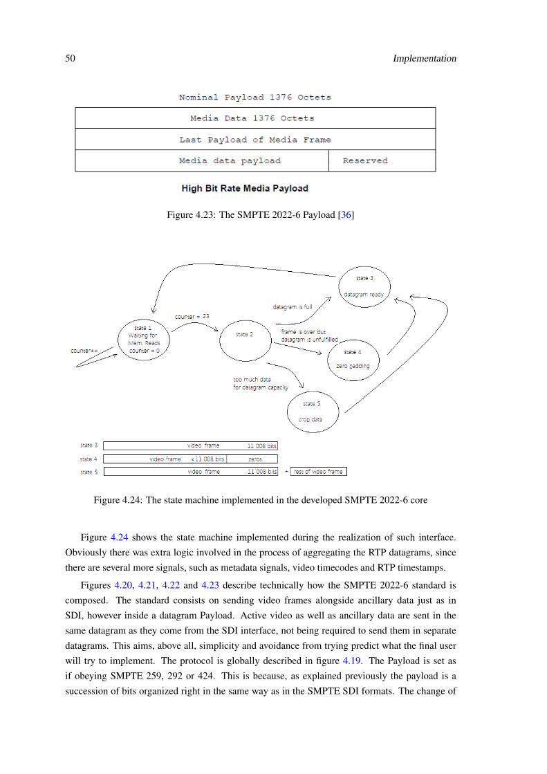
50 Implementation
Figure 4.23: The SMPTE 2022-6 Payload [36]
Figure 4.24: The state machine implemented in the developed SMPTE 2022-6 core
Figure 4.24 shows the state machine implemented during the realization of such interface.
Obviously there was extra logic involved in the process of aggregating the RTP datagrams, since
there are several more signals, such as metadata signals, video timecodes and RTP timestamps.
Figures 4.20, 4.21, 4.22 and 4.23 describe technically how the SMPTE 2022-6 standard is
composed. The standard consists on sending video frames alongside ancillary data just as in
SDI, however inside a datagram Payload. Active video as well as ancillary data are sent in the
same datagram as they come from the SDI interface, not being required to send them in separate
datagrams. This aims, above all, simplicity and avoidance from trying predict what the final user
will try to implement. The protocol is globally described in figure 4.19. The Payload is set as
if obeying SMPTE 259, 292 or 424. This is because, as explained previously the payload is a
succession of bits organized right in the same way as in the SMPTE SDI formats. The change of
4.5 SMPTE 2022-6 51
platform is provided due to Headers containing Metadata and Network information. In this project
the SMPTE 2022-6 Payload is following the SMPTE ST 424 for 3G-SDI Video.
Table 4.6: RTP Header Fields
Field Bits DescriptionV 2 Version of RTP protocol - set to 2P 1 Padding definitions - set to 0X 1 Header Extension - set to 0
CC 4 CSRC count - set to 0M 1 Marker - set to 1 in last videoframe datagramPT 7 Payload Type - 98 without FEC, 99 with FEC
sequence number 16 The low order bits for RTP sequence countertimestamp 32 RTP timestamp
SSRC 32 Synchronization source
Table 4.7: SMPTE 2022-6 Header Fields
Field Bits DescriptionExt 4 Payload extension - set to 0F 1 Video source format flag - set to 1
VSID 3 Video source ID - set to 0FRCount 8 Frame Counter - increases when frame changes
R 2 Reference for time stamp - set to private time referenceS 2 Video Payload Scrambling - set to 0
FEC 3 Forward Error Correction - set to 0, not used
CF 4Clock Frequency - clock frequency of the payload video
148.5MHz per wordRESERVE 5 Set to 0. Reserved for future use.
MAP 4Define which standard is set in the payload.
(SMPTE 424)FRAME 8 Frame resolution and structure.FRATE 8 Frame rate.
SAMPLE 4 Sample structure and bit depth.FMT-RESERVE 8 Reserved for future use.Video timestamp 32 Sourced from the video timecodesHeader extension 32 Not used.
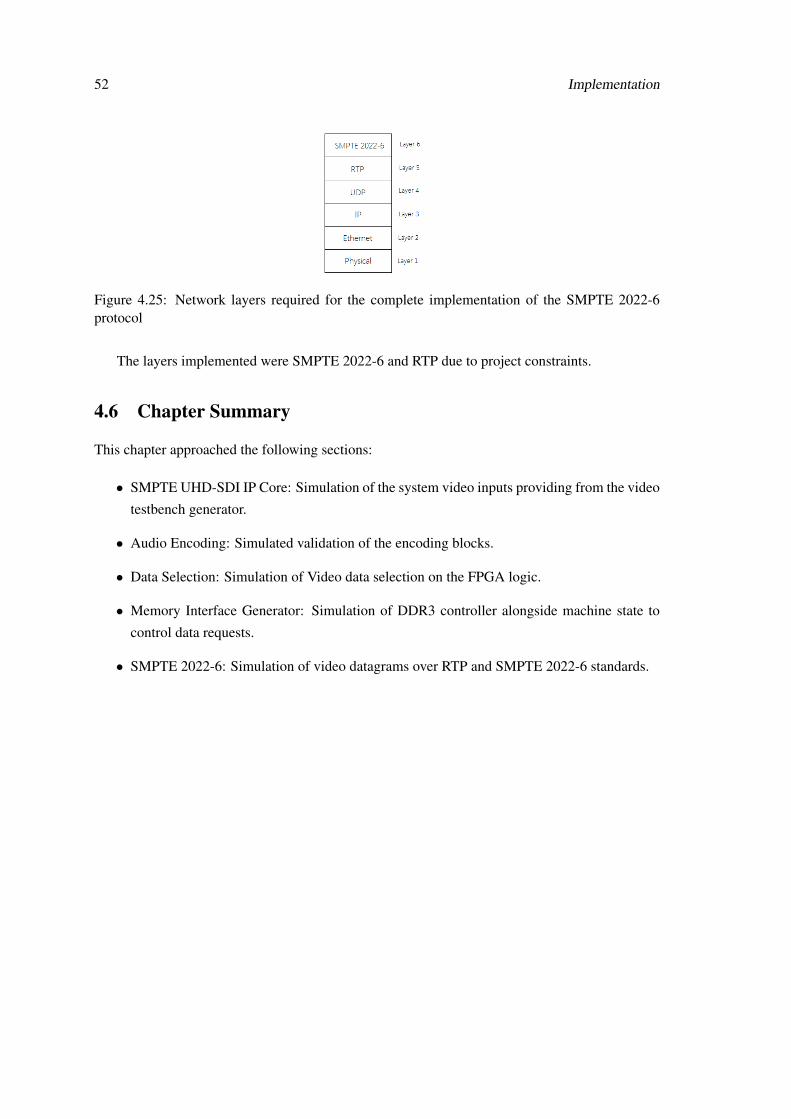
52 Implementation
Figure 4.25: Network layers required for the complete implementation of the SMPTE 2022-6protocol
The layers implemented were SMPTE 2022-6 and RTP due to project constraints.
4.6 Chapter Summary
This chapter approached the following sections:
• SMPTE UHD-SDI IP Core: Simulation of the system video inputs providing from the video
testbench generator.
• Audio Encoding: Simulated validation of the encoding blocks.
• Data Selection: Simulation of Video data selection on the FPGA logic.
• Memory Interface Generator: Simulation of DDR3 controller alongside machine state to
control data requests.
• SMPTE 2022-6: Simulation of video datagrams over RTP and SMPTE 2022-6 standards.
Chapter 5
Functional Verification
In order to verify the simulated system, a real prototype was built. The present chapter is orga-
nized in order to describe how the implemented system was validated after the construction of the
prototype, as well as the implementation of dynamic partial reconfiguration. The most important
verification stages are divided in sections. The chapter starts with a section giving some insight
on the 7 series GTX transceivers technology and usage, covers the SMPTE UHD-SDI integra-
tion on a physical interface, details how the validation system was built and verified and explains
how the validation tools should be used. The system was fully verified by manually analyzing the
output datagram bits corresponding to the RTP protocol. The logic behind the developed system
introduces an approximate video delay of 601 clock cycles. This value was calculated by adding
up the sequential delays introduced by the different modules developed for the video changing
of transport platform. One clock cycle is required to convert audio, 25 clock cycles are required
to gather enough video data to perform a 500 bit size memory write. And 23 memory reads are
required to gather up an RTP complete datagram. Since each memory read takes in average 25
clock cycles to be answered, it takes 25x23 memory cycles to gather an RTP datagram. Therefore
1+25+(25x23) = 601. At 148.5MHz, this produces a system minimum delay of 4 μs. This does
not have into account future network latencies, but only video processing logic.
5.1 Implementation Changes
Due to the constraints explained on chapter 3, the MIG - DDR3 Ram controller could not be im-
plemented. Having in mind that memory space is critical in real industry systems, but constrained
by project resources, the DDR3 Ram memory was replaced by internal FPGA Block ram. The
BRAM controller behaves in the same way with similar signals, with difference of much better
performance. The BRAM controller signals are described on the table below:
53
54 Functional Verification
Table 5.1: BRAM control signals
clka Memory clock.ena Enables reads and writes.
weaWrite command. When asserted to 0performs a read if ena is asserted.
addra Memory address.dina Data write bus.douta Data read bus.
However, it is noticeable how there is no equivalent to app_rd_valid signal indicating when
requested data appears on the reading bus. This is because the BRAM controller performance
returns the requested data in the following cycle to the request. In opposition to the MIG - DDR3
controller, that could take dozens of clock cycles, the BRAM controller performs much better.
However, because it is internal to the FPGA, its size is restricted and it would waste plenty more
hardware if implemented on an industrial product. It works as expected in the developed prototype
though.
5.2 GTX Transceivers
High Speed transceivers are a critical feature, since they allow high speed inputs and outputs.
High Speed transceivers are a serializer-deserializer capable of operating at serial bit rates above
1 Gbps. They enable the pseudo video signal generator to be implemented on the FPGA logic and
looped back in order to provide system inputs. Therefore the 7 series transceivers were the most
critical constituent of the physical prototype.
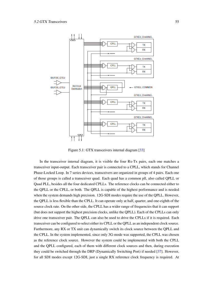
5.2 GTX Transceivers 55
Figure 5.1: GTX transceivers internal diagram [33]
In the transceiver internal diagram, it is visible the four Rx-Tx pairs, each one matches a
transceiver input-output. Each transceiver pair is connected to a CPLL, which stands for Channel
Phase-Locked Loop. In 7 series devices, transceivers are organized in groups of 4 pairs. Each one
of those groups is called a transceiver quad. Each quad has a common pll, also called QPLL or
Quad PLL, besides all the four dedicated CPLLs. The reference clocks can be connected either to
the QPLL or the CPLL, or both. The QPLL is capable of the highest performance and is needed
when the system demands high precision. 12G-SDI modes require the use of the QPLL. However,
the QPLL is less flexible than the CPLL. It can operate only at half, quarter, and one-eighth of the
source clock rate. On the other side, the CPLL has a wider range of frequencies that it can support
(but does not support the highest precision clocks, unlike the QPLL). Each of the CPLLs can only
drive one transceiver pair. The QPLL can also be used to drive the CPLLs if it is required. Each
transceiver can be configured to select either its CPLL or the QPLL as an independent clock source.
Furthermore, any RX or TX unit can dynamically switch its clock source between the QPLL and
the CPLL. In the system implemented, since only 3G-mode was supported, the CPLL was chosen
as the reference clock source. However the system could be implemented with both the CPLL
and the QPLL configured, each of them with different clock sources and then, during execution
they could be switched through the DRP (Dynamically Switching Port) if needed [37]. However,
for all SDI modes except 12G-SDI, just a single RX reference clock frequency is required. At
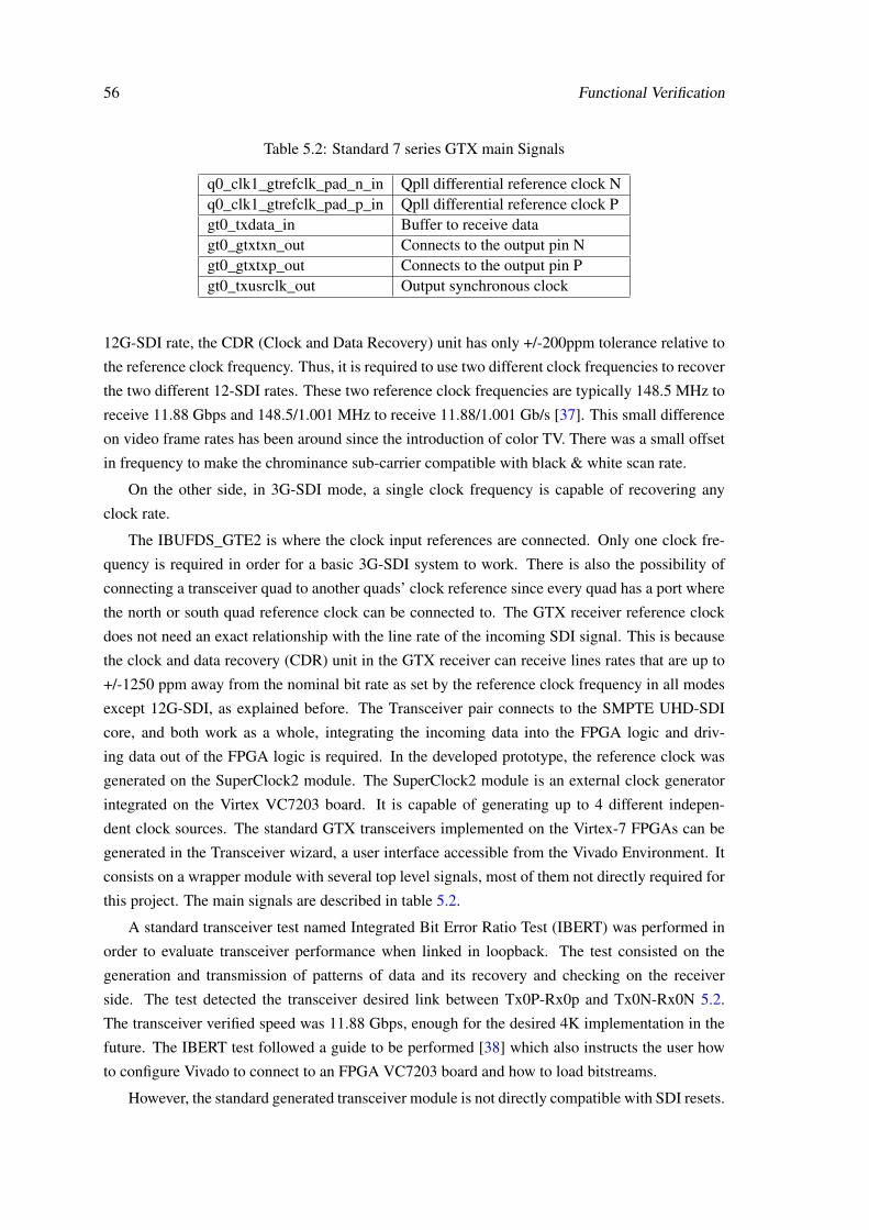
56 Functional Verification
Table 5.2: Standard 7 series GTX main Signals
q0_clk1_gtrefclk_pad_n_in Qpll differential reference clock Nq0_clk1_gtrefclk_pad_p_in Qpll differential reference clock Pgt0_txdata_in Buffer to receive datagt0_gtxtxn_out Connects to the output pin Ngt0_gtxtxp_out Connects to the output pin Pgt0_txusrclk_out Output synchronous clock
12G-SDI rate, the CDR (Clock and Data Recovery) unit has only +/-200ppm tolerance relative to
the reference clock frequency. Thus, it is required to use two different clock frequencies to recover
the two different 12-SDI rates. These two reference clock frequencies are typically 148.5 MHz to
receive 11.88 Gbps and 148.5/1.001 MHz to receive 11.88/1.001 Gb/s [37]. This small difference
on video frame rates has been around since the introduction of color TV. There was a small offset
in frequency to make the chrominance sub-carrier compatible with black & white scan rate.
On the other side, in 3G-SDI mode, a single clock frequency is capable of recovering any
clock rate.
The IBUFDS_GTE2 is where the clock input references are connected. Only one clock fre-
quency is required in order for a basic 3G-SDI system to work. There is also the possibility of
connecting a transceiver quad to another quads’ clock reference since every quad has a port where
the north or south quad reference clock can be connected to. The GTX receiver reference clock
does not need an exact relationship with the line rate of the incoming SDI signal. This is because
the clock and data recovery (CDR) unit in the GTX receiver can receive lines rates that are up to
+/-1250 ppm away from the nominal bit rate as set by the reference clock frequency in all modes
except 12G-SDI, as explained before. The Transceiver pair connects to the SMPTE UHD-SDI
core, and both work as a whole, integrating the incoming data into the FPGA logic and driv-
ing data out of the FPGA logic is required. In the developed prototype, the reference clock was
generated on the SuperClock2 module. The SuperClock2 module is an external clock generator
integrated on the Virtex VC7203 board. It is capable of generating up to 4 different indepen-
dent clock sources. The standard GTX transceivers implemented on the Virtex-7 FPGAs can be
generated in the Transceiver wizard, a user interface accessible from the Vivado Environment. It
consists on a wrapper module with several top level signals, most of them not directly required for
this project. The main signals are described in table 5.2.
A standard transceiver test named Integrated Bit Error Ratio Test (IBERT) was performed in
order to evaluate transceiver performance when linked in loopback. The test consisted on the
generation and transmission of patterns of data and its recovery and checking on the receiver
side. The test detected the transceiver desired link between Tx0P-Rx0p and Tx0N-Rx0N 5.2.
The transceiver verified speed was 11.88 Gbps, enough for the desired 4K implementation in the
future. The IBERT test followed a guide to be performed [38] which also instructs the user how
to configure Vivado to connect to an FPGA VC7203 board and how to load bitstreams.
However, the standard generated transceiver module is not directly compatible with SDI resets.
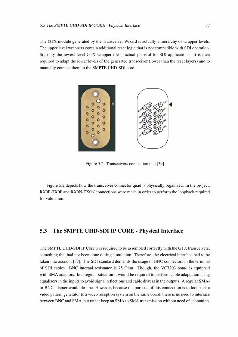
5.3 The SMPTE UHD-SDI IP CORE - Physical Interface 57
The GTX module generated by the Transceiver Wizard is actually a hierarchy of wrapper levels.
The upper level wrappers contain additional reset logic that is not compatible with SDI operation.
So, only the lowest level GTX wrapper file is actually useful for SDI applications. It is then
required to adapt the lower levels of the generated transceiver (lower than the reset layers) and to
manually connect them to the SMPTE UHD-SDI core.
Figure 5.2: Transceivers connection pad [39]
Figure 5.2 depicts how the transceiver connector quad is physically organized. In the project,
RX0P-TX0P and RX0N-TX0N connections were made in order to perform the loopback required
for validation.
5.3 The SMPTE UHD-SDI IP CORE - Physical Interface
The SMPTE UHD-SDI IP Core was required to be assembled correctly with the GTX transceivers,
something that had not been done during simulation. Therefore, the electrical interface had to be
taken into account [37]. The SDI standard demands the usage of BNC connectors in the terminal
of SDI cables. BNC internal resistance is 75 Ohm. Though, the VC7203 board is equipped
with SMA adaptors. In a regular situation it would be required to perform cable adaptation using
equalizers in the inputs to avoid signal reflections and cable drivers in the outputs. A regular SMA-
to-BNC adapter would do fine. However, because the purpose of this connection is to loopback a
video pattern generator to a video reception system on the same board, there is no need to interface
between BNC and SMA, but rather keep an SMA to SMA transmission without need of adaptation.
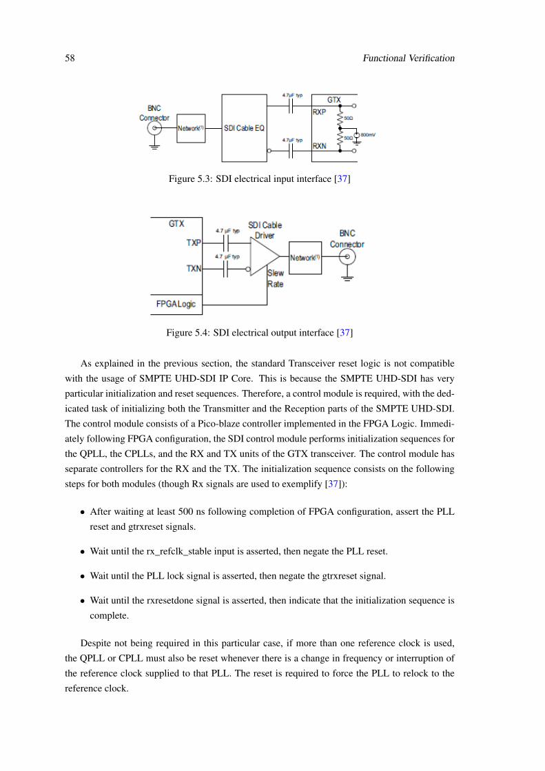
58 Functional Verification
Figure 5.3: SDI electrical input interface [37]
Figure 5.4: SDI electrical output interface [37]
As explained in the previous section, the standard Transceiver reset logic is not compatible
with the usage of SMPTE UHD-SDI IP Core. This is because the SMPTE UHD-SDI has very
particular initialization and reset sequences. Therefore, a control module is required, with the ded-
icated task of initializing both the Transmitter and the Reception parts of the SMPTE UHD-SDI.
The control module consists of a Pico-blaze controller implemented in the FPGA Logic. Immedi-
ately following FPGA configuration, the SDI control module performs initialization sequences for
the QPLL, the CPLLs, and the RX and TX units of the GTX transceiver. The control module has
separate controllers for the RX and the TX. The initialization sequence consists on the following
steps for both modules (though Rx signals are used to exemplify [37]):
• After waiting at least 500 ns following completion of FPGA configuration, assert the PLL
reset and gtrxreset signals.
• Wait until the rx_refclk_stable input is asserted, then negate the PLL reset.
• Wait until the PLL lock signal is asserted, then negate the gtrxreset signal.
• Wait until the rxresetdone signal is asserted, then indicate that the initialization sequence is
complete.
Despite not being required in this particular case, if more than one reference clock is used,
the QPLL or CPLL must also be reset whenever there is a change in frequency or interruption of
the reference clock supplied to that PLL. The reset is required to force the PLL to relock to the
reference clock.
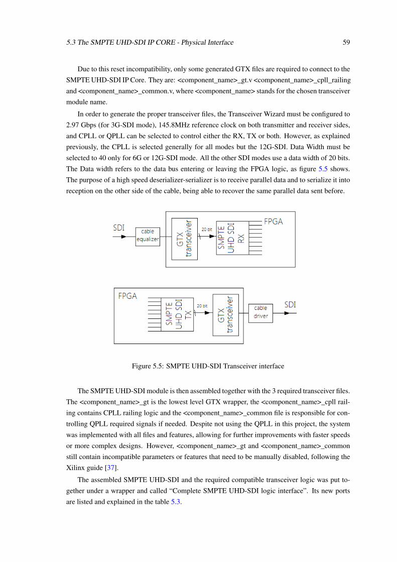
5.3 The SMPTE UHD-SDI IP CORE - Physical Interface 59
Due to this reset incompatibility, only some generated GTX files are required to connect to the
SMPTE UHD-SDI IP Core. They are: <component_name>_gt.v <component_name>_cpll_railing
and <component_name>_common.v, where <component_name> stands for the chosen transceiver
module name.
In order to generate the proper transceiver files, the Transceiver Wizard must be configured to
2.97 Gbps (for 3G-SDI mode), 145.8MHz reference clock on both transmitter and receiver sides,
and CPLL or QPLL can be selected to control either the RX, TX or both. However, as explained
previously, the CPLL is selected generally for all modes but the 12G-SDI. Data Width must be
selected to 40 only for 6G or 12G-SDI mode. All the other SDI modes use a data width of 20 bits.
The Data width refers to the data bus entering or leaving the FPGA logic, as figure 5.5 shows.
The purpose of a high speed deserializer-serializer is to receive parallel data and to serialize it into
reception on the other side of the cable, being able to recover the same parallel data sent before.
Figure 5.5: SMPTE UHD-SDI Transceiver interface
The SMPTE UHD-SDI module is then assembled together with the 3 required transceiver files.
The <component_name>_gt is the lowest level GTX wrapper, the <component_name>_cpll rail-
ing contains CPLL railing logic and the <component_name>_common file is responsible for con-
trolling QPLL required signals if needed. Despite not using the QPLL in this project, the system
was implemented with all files and features, allowing for further improvements with faster speeds
or more complex designs. However, <component_name>_gt and <component_name>_common
still contain incompatible parameters or features that need to be manually disabled, following the
Xilinx guide [37].
The assembled SMPTE UHD-SDI and the required compatible transceiver logic was put to-
gether under a wrapper and called “Complete SMPTE UHD-SDI logic interface”. Its new ports
are listed and explained in the table 5.3.
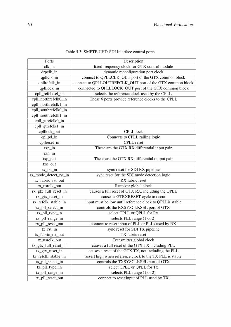
60 Functional Verification
Table 5.3: SMPTE UHD-SDI Interface control ports
Ports Descriptionclk_in fixed frequency clock for GTX control module
drpclk_in dynamic reconfiguration port clockqpllclk_in connect to QPLLCLK_OUT port of the GTX common block
qpllrefclk_in connect to QPLLOUTREFCLK_OUT port of the GTX common blockqplllock_in connected to QPLLLOCK_OUT port of the GTX common block
cpll_refclksel_in selects the reference clock used by the CPLLcpll_northrefclk0_in These 6 ports provide reference clocks to the CPLLcpll_northrefclk1_incpll_southrefclk0_incpll_southrefclk1_in
cpll_gtrefclk0_incpll_gtrefclk1_in
cplllock_out CPLL lockcpllpd_in Connects to CPLL railing logic
cpllreset_in CPLL resetrxp_in These are the GTX RX differential input pairrxn_intxp_out These are the GTX RX differential output pairtxn_out
rx_rst_in sync reset for SDI RX pipelinerx_mode_detect_rst_in sync reset for the SDI mode detection logic
rx_fabric_rst_out RX fabric resetrx_usrclk_out Receiver global clock
rx_gtx_full_reset_in causes a full reset of GTX RX, including the QPLLrx_gtx_reset_in causes a GTRXRESET cycle to occur
rx_refclk_stable_in input must be low until reference clock to QPLLis stablerx_pll_select_in controls the RXSYSCLKSEL port of GTXrx_pll_type_in select CPLL or QPLL for Rxrx_pll_range_in selects PLL range (1 or 2)rx_pll_reset_out connect to reset input of PLL or PLLs used by RX
tx_rst_in sync reset for SDI TX pipelinetx_fabric_rst_out TX fabric reset
tx_usrclk_out Transmitter global clocktx_gtx_full_reset_in causes a full reset of the GTX TX including PLL
tx_gtx_reset_in causes a reset of the GTX TX, not including the PLLtx_refclk_stable_in assert high when reference clock to the TX PLL is stable
tx_pll_select_in controls the TXSYSCLKSEL port of GTXtx_pll_type_in select CPLL or QPLL for Txtx_pll_range_in selects PLL range (1 or 2)tx_pll_reset_out connect to reset input of PLL used by TX
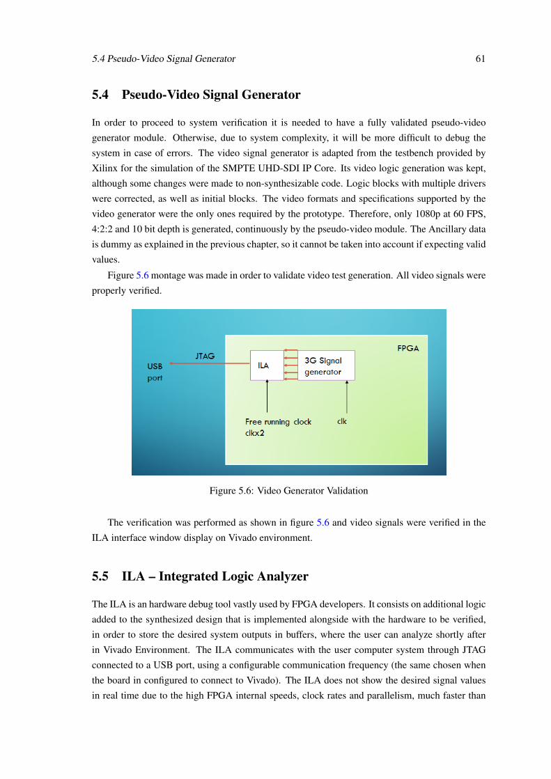
5.4 Pseudo-Video Signal Generator 61
5.4 Pseudo-Video Signal Generator
In order to proceed to system verification it is needed to have a fully validated pseudo-video
generator module. Otherwise, due to system complexity, it will be more difficult to debug the
system in case of errors. The video signal generator is adapted from the testbench provided by
Xilinx for the simulation of the SMPTE UHD-SDI IP Core. Its video logic generation was kept,
although some changes were made to non-synthesizable code. Logic blocks with multiple drivers
were corrected, as well as initial blocks. The video formats and specifications supported by the
video generator were the only ones required by the prototype. Therefore, only 1080p at 60 FPS,
4:2:2 and 10 bit depth is generated, continuously by the pseudo-video module. The Ancillary data
is dummy as explained in the previous chapter, so it cannot be taken into account if expecting valid
values.
Figure 5.6 montage was made in order to validate video test generation. All video signals were
properly verified.
Figure 5.6: Video Generator Validation
The verification was performed as shown in figure 5.6 and video signals were verified in the
ILA interface window display on Vivado environment.
5.5 ILA – Integrated Logic Analyzer
The ILA is an hardware debug tool vastly used by FPGA developers. It consists on additional logic
added to the synthesized design that is implemented alongside with the hardware to be verified,
in order to store the desired system outputs in buffers, where the user can analyze shortly after
in Vivado Environment. The ILA communicates with the user computer system through JTAG
connected to a USB port, using a configurable communication frequency (the same chosen when
the board in configured to connect to Vivado). The ILA does not show the desired signal values
in real time due to the high FPGA internal speeds, clock rates and parallelism, much faster than
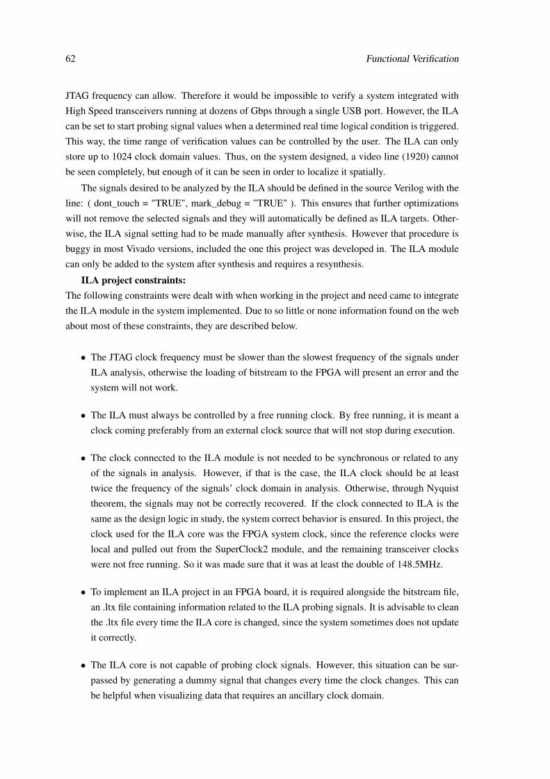
62 Functional Verification
JTAG frequency can allow. Therefore it would be impossible to verify a system integrated with
High Speed transceivers running at dozens of Gbps through a single USB port. However, the ILA
can be set to start probing signal values when a determined real time logical condition is triggered.
This way, the time range of verification values can be controlled by the user. The ILA can only
store up to 1024 clock domain values. Thus, on the system designed, a video line (1920) cannot
be seen completely, but enough of it can be seen in order to localize it spatially.
The signals desired to be analyzed by the ILA should be defined in the source Verilog with the
line: ( dont_touch = "TRUE", mark_debug = "TRUE" ). This ensures that further optimizations
will not remove the selected signals and they will automatically be defined as ILA targets. Other-
wise, the ILA signal setting had to be made manually after synthesis. However that procedure is
buggy in most Vivado versions, included the one this project was developed in. The ILA module
can only be added to the system after synthesis and requires a resynthesis.
ILA project constraints:The following constraints were dealt with when working in the project and need came to integrate
the ILA module in the system implemented. Due to so little or none information found on the web
about most of these constraints, they are described below.
• The JTAG clock frequency must be slower than the slowest frequency of the signals under
ILA analysis, otherwise the loading of bitstream to the FPGA will present an error and the
system will not work.
• The ILA must always be controlled by a free running clock. By free running, it is meant a
clock coming preferably from an external clock source that will not stop during execution.
• The clock connected to the ILA module is not needed to be synchronous or related to any
of the signals in analysis. However, if that is the case, the ILA clock should be at least
twice the frequency of the signals’ clock domain in analysis. Otherwise, through Nyquist
theorem, the signals may not be correctly recovered. If the clock connected to ILA is the
same as the design logic in study, the system correct behavior is ensured. In this project, the
clock used for the ILA core was the FPGA system clock, since the reference clocks were
local and pulled out from the SuperClock2 module, and the remaining transceiver clocks
were not free running. So it was made sure that it was at least the double of 148.5MHz.
• To implement an ILA project in an FPGA board, it is required alongside the bitstream file,
an .ltx file containing information related to the ILA probing signals. It is advisable to clean
the .ltx file every time the ILA core is changed, since the system sometimes does not update
it correctly.
• The ILA core is not capable of probing clock signals. However, this situation can be sur-
passed by generating a dummy signal that changes every time the clock changes. This can
be helpful when visualizing data that requires an ancillary clock domain.
5.6 Dynamic Partial Reconfiguration 63
Figure 5.7: ILA core usage
The ILA core usage can be seen at figure 5.7.
5.6 Dynamic Partial Reconfiguration
Dynamic Partial Reconfiguration was one feature that couldn’t be simulated in the project imple-
mentation stage. Therefore its implementation took place on the prototype construction step. To
start with, a Dynamic Partial Reconfiguration Xilinx Tutorial [40] was performed. Not all FPGA
families support partial reconfiguration. The tutorial was targeted to a Kintex KC705 demonstra-
tion board, but was adapted to the Virtex VC7203 during the realization of this project. After the
realization of this tutorial, partial reconfiguration was applied to the project. A set of files were
provided alongside the tutorial on the Xilinx website. The archive contains a hierarchy of folders
destined to organize partial and static synthesis, bitstreams and implementations as well as check-
points and source files. The files contained a set of .TCL scripts that allowed the user to synthesize,
place, route and optimize all the files in which partial reconfiguration was to be applied to. The
intended partial reconfiguration implementation is as follows in figure 5.8.
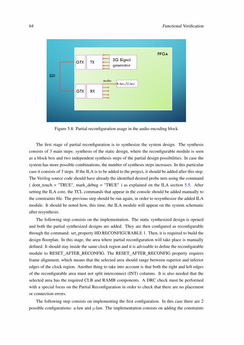
64 Functional Verification
Figure 5.8: Partial reconfiguration usage in the audio encoding block
The first stage of partial reconfiguration is to synthesize the system design. The synthesis
consists of 3 main steps: synthesis of the static design, where the reconfigurable module is seen
as a block box and two independent synthesis steps of the partial design possibilities. In case the
system has more possible combinations, the number of synthesis steps increases. In this particular
case it consists of 3 steps. If the ILA is to be added to the project, it should be added after this step.
The Verilog source code should have already the identified desired probe nets using the command
( dont_touch = "TRUE", mark_debug = "TRUE" ) as explained on the ILA section 5.5. After
setting the ILA core, the TCL commands that appear in the console should be added manually to
the constraints file. The previous step should be run again, in order to resynthesize the added ILA
module. It should be noted how, this time, the ILA module will appear on the system schematic
after resynthesis.
The following step consists on the implementation. The static synthesized design is opened
and both the partial synthesized designs are added. They are then configured as reconfigurable
through the command: set_property HD.RECONFIGURABLE 1. Then, it is required to build the
design floorplan. In this stage, the area where partial reconfiguration will take place is manually
defined. It should stay inside the same clock region and it is advisable to define the reconfigurable
module to RESET_AFTER_RECONFIG. The RESET_AFTER_RECONFIG property requires
frame alignment, which means that the selected area should range between superior and inferior
edges of the clock region. Another thing to take into account is that both the right and left edges
of the reconfigurable area must not split interconnect (INT) columns. It is also needed that the
selected area has the required CLB and RAMB components. A DRC check must be performed
with a special focus on the Partial Reconfiguration in order to check that there are no placement
or connection errors.
The following step consists on implementing the first configuration. In this case there are 2
possible configurations: a-law and μ-law. The implementation consists on adding the constraints
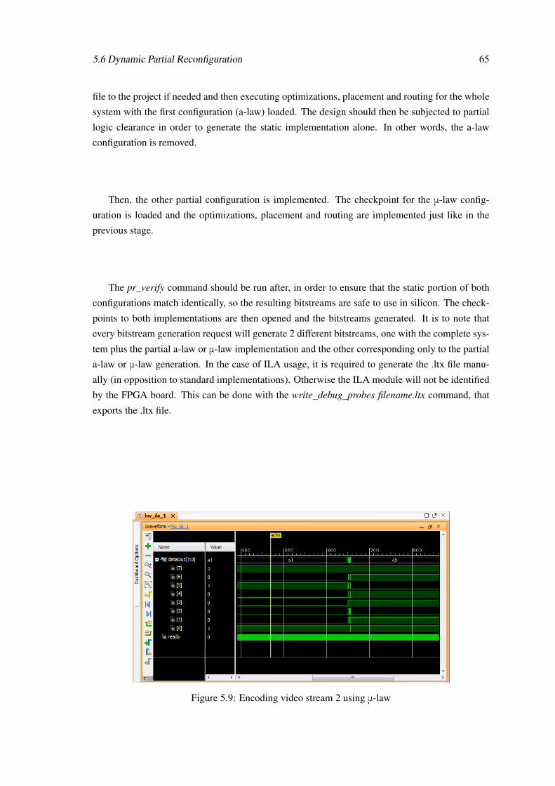
5.6 Dynamic Partial Reconfiguration 65
file to the project if needed and then executing optimizations, placement and routing for the whole
system with the first configuration (a-law) loaded. The design should then be subjected to partial
logic clearance in order to generate the static implementation alone. In other words, the a-law
configuration is removed.
Then, the other partial configuration is implemented. The checkpoint for the μ-law config-
uration is loaded and the optimizations, placement and routing are implemented just like in the
previous stage.
The pr_verify command should be run after, in order to ensure that the static portion of both
configurations match identically, so the resulting bitstreams are safe to use in silicon. The check-
points to both implementations are then opened and the bitstreams generated. It is to note that
every bitstream generation request will generate 2 different bitstreams, one with the complete sys-
tem plus the partial a-law or μ-law implementation and the other corresponding only to the partial
a-law or μ-law generation. In the case of ILA usage, it is required to generate the .ltx file manu-
ally (in opposition to standard implementations). Otherwise the ILA module will not be identified
by the FPGA board. This can be done with the write_debug_probes filename.ltx command, that
exports the .ltx file.
Figure 5.9: Encoding video stream 2 using μ-law
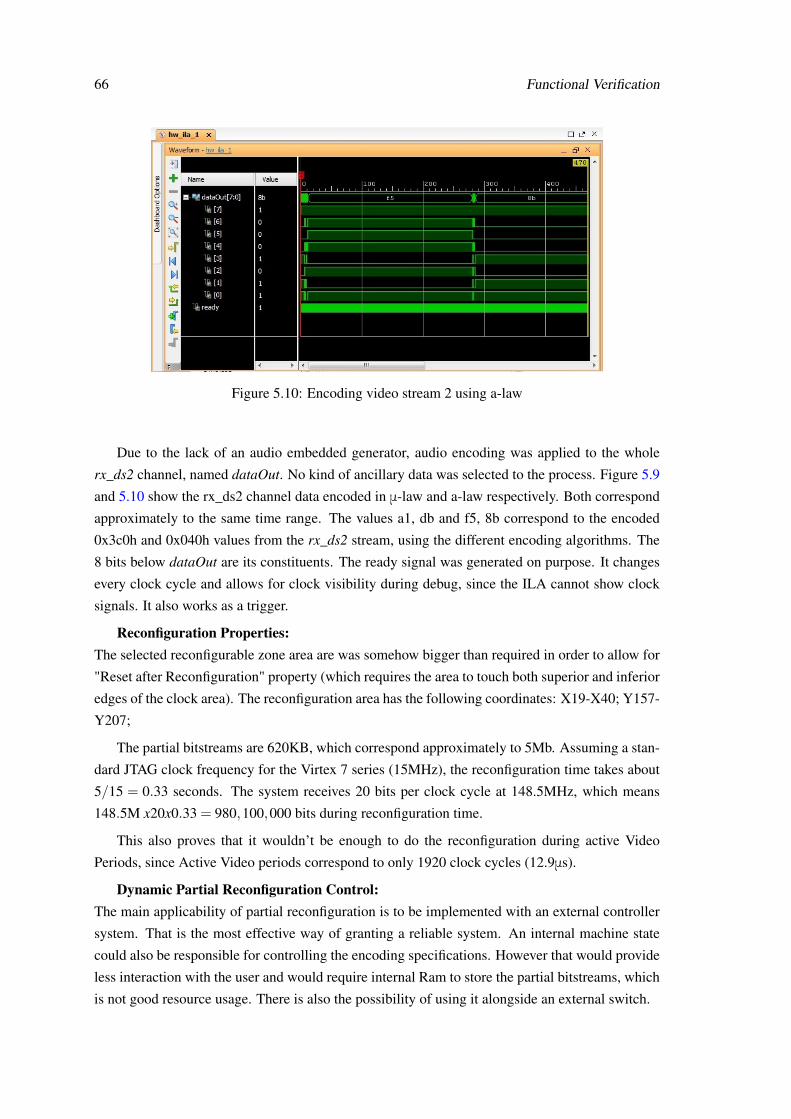
66 Functional Verification
Figure 5.10: Encoding video stream 2 using a-law
Due to the lack of an audio embedded generator, audio encoding was applied to the whole
rx_ds2 channel, named dataOut. No kind of ancillary data was selected to the process. Figure 5.9
and 5.10 show the rx_ds2 channel data encoded in μ-law and a-law respectively. Both correspond
approximately to the same time range. The values a1, db and f5, 8b correspond to the encoded
0x3c0h and 0x040h values from the rx_ds2 stream, using the different encoding algorithms. The
8 bits below dataOut are its constituents. The ready signal was generated on purpose. It changes
every clock cycle and allows for clock visibility during debug, since the ILA cannot show clock
signals. It also works as a trigger.
Reconfiguration Properties:The selected reconfigurable zone area are was somehow bigger than required in order to allow for
"Reset after Reconfiguration" property (which requires the area to touch both superior and inferior
edges of the clock area). The reconfiguration area has the following coordinates: X19-X40; Y157-
Y207;
The partial bitstreams are 620KB, which correspond approximately to 5Mb. Assuming a stan-
dard JTAG clock frequency for the Virtex 7 series (15MHz), the reconfiguration time takes about
5/15 = 0.33 seconds. The system receives 20 bits per clock cycle at 148.5MHz, which means
148.5M x20x0.33 = 980,100,000 bits during reconfiguration time.
This also proves that it wouldn’t be enough to do the reconfiguration during active Video
Periods, since Active Video periods correspond to only 1920 clock cycles (12.9μs).
Dynamic Partial Reconfiguration Control:The main applicability of partial reconfiguration is to be implemented with an external controller
system. That is the most effective way of granting a reliable system. An internal machine state
could also be responsible for controlling the encoding specifications. However that would provide
less interaction with the user and would require internal Ram to store the partial bitstreams, which
is not good resource usage. There is also the possibility of using it alongside an external switch.
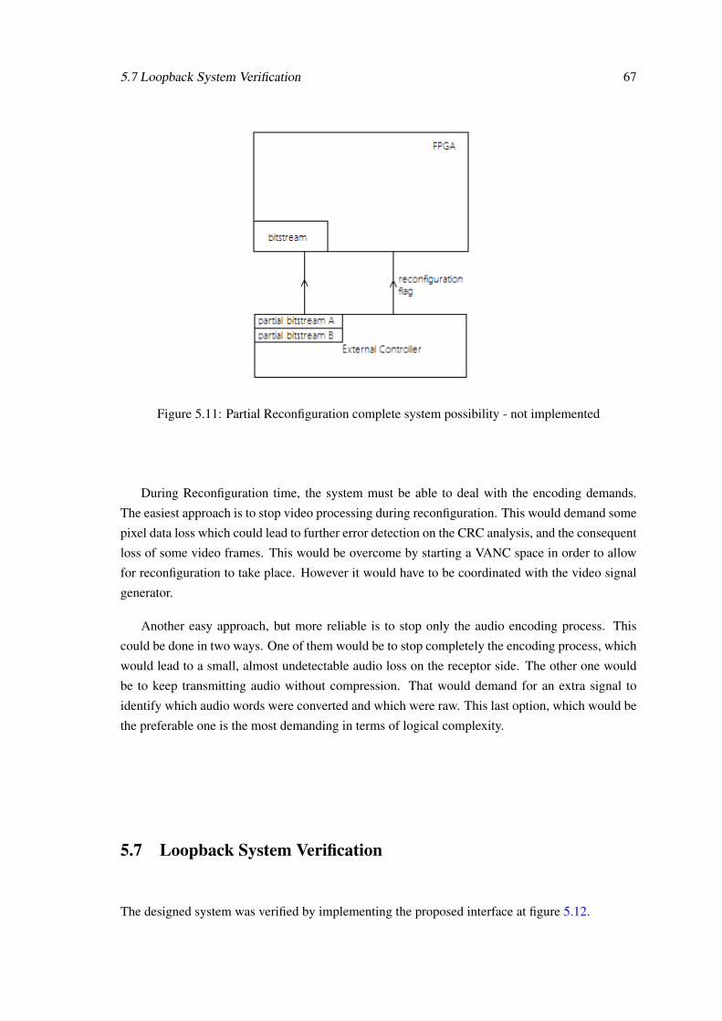
5.7 Loopback System Verification 67
Figure 5.11: Partial Reconfiguration complete system possibility - not implemented
During Reconfiguration time, the system must be able to deal with the encoding demands.
The easiest approach is to stop video processing during reconfiguration. This would demand some
pixel data loss which could lead to further error detection on the CRC analysis, and the consequent
loss of some video frames. This would be overcome by starting a VANC space in order to allow
for reconfiguration to take place. However it would have to be coordinated with the video signal
generator.
Another easy approach, but more reliable is to stop only the audio encoding process. This
could be done in two ways. One of them would be to stop completely the encoding process, which
would lead to a small, almost undetectable audio loss on the receptor side. The other one would
be to keep transmitting audio without compression. That would demand for an extra signal to
identify which audio words were converted and which were raw. This last option, which would be
the preferable one is the most demanding in terms of logical complexity.
5.7 Loopback System Verification
The designed system was verified by implementing the proposed interface at figure 5.12.
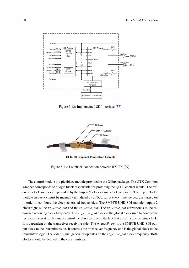
68 Functional Verification
Figure 5.12: Implemented SDI interface [37]
Figure 5.13: Loopback connection between RX-TX [39]
The control module is a picoblaze module provided in the Xilinx package. The GTX Common
wrapper corresponds to a logic block responsible for providing the QPLL control inputs. The ref-
erence clock sources are provided by the SuperClock2 external clock generator. The SuperClock2
module frequency must be manually initialized by a .TCL script every time the board is turned on
in order to configure the clock generated frequencies. The SMPTE UHD-SDI module outputs 2
clock signals, the rx_usrclk_out and the tx_usrclk_out. The rx_usrclk_out corresponds to the re-
covered receiving clock frequency. The rx_usrclk_out clock is the global clock used to control the
receiver side system. It cannot control the ILA core due to the fact that it isn’t a free running clock.
It is dependent on the transceiver receiving side. The tx_usrclk_out is the SMPTE UHD-SDI out-
put clock to the transmitter side. It controls the transceiver frequency and is the global clock to the
transmitter logic. The video signal generator operates on the tx_usrclk_out clock frequency. Both
clocks should be defined in the constraints as:
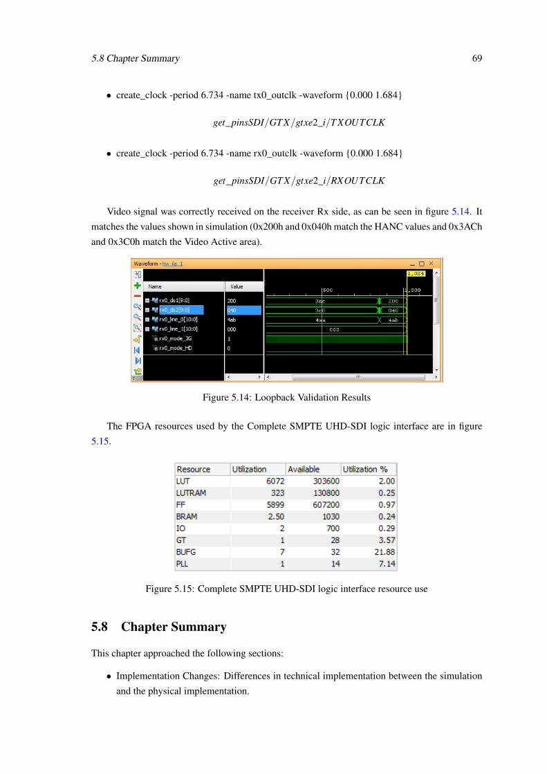
5.8 Chapter Summary 69
• create_clock -period 6.734 -name tx0_outclk -waveform {0.000 1.684}
get_pinsSDI/GT X/gtxe2_i/T XOUTCLK
• create_clock -period 6.734 -name rx0_outclk -waveform {0.000 1.684}
get_pinsSDI/GT X/gtxe2_i/RXOUTCLK
Video signal was correctly received on the receiver Rx side, as can be seen in figure 5.14. It
matches the values shown in simulation (0x200h and 0x040h match the HANC values and 0x3ACh
and 0x3C0h match the Video Active area).
Figure 5.14: Loopback Validation Results
The FPGA resources used by the Complete SMPTE UHD-SDI logic interface are in figure
5.15.
Figure 5.15: Complete SMPTE UHD-SDI logic interface resource use
5.8 Chapter Summary
This chapter approached the following sections:
• Implementation Changes: Differences in technical implementation between the simulation
and the physical implementation.
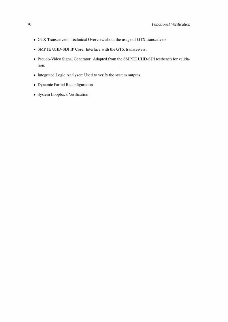
70 Functional Verification
• GTX Transceivers: Technical Overview about the usage of GTX transceivers.
• SMPTE UHD-SDI IP Core: Interface with the GTX transceivers.
• Pseudo-Video Signal Generator: Adapted from the SMPTE UHD-SDI testbench for valida-
tion.
• Integrated Logic Analyzer: Used to verify the system outputs.
• Dynamic Partial Reconfiguration
• System Loopback Verification
Chapter 6
Conclusions
6.1 Work Summary
The system designed and validated on the previous chapters was composed of multiple IP Cores
and tools, as well as self-developed modules during the realization of this project. In the first stage,
the whole system was simulated and validated through simulation and its outputs were manually
analysed. In the second stage, a prototype was built in order to show the feasibility of the simulated
design.
The first step of the project consisted on the assembly of an SMPTE UHD-SDI video interface
to a Data Select Module (designed in verilog for the project) that follows a set of SMPTE Standards
in order to detect and output Ancillary data as well as active video pixel data. One of the video
streams assumed to contain audio information (since embedded audio could not be generated)
was connected to an audio encoder, and dynamic reconfiguration was applied, allowing switching
between a-law or μ-law encoding.
The Data Select Module, as well as the audio encoder, were then connected to a DDR3 con-
troller that was responsible for organizing video data and ancillary data on the DDR3 RAM fol-
lowing a memory map (designed in verilog for the project).
The DDR3 RAM controller was then connected to a SMPTE 2022-6 (designed in verilog
for the project) in order to provide the video data from the RAM and for it to be assembled in
network Datagrams following both the RTP protocol as well as the SMPTE 2022-6 Standard for
Video Over IP. The DDR3 module had to be replaced by internal FPGA BRAM in the physical
implementation of the prototype, due to board connectivity constraints.
The feasibility of the prototype for uncompressed HD video resolutions and its features was
shown, as well as its tools and critical features analysed.
The system was fully verified by manually analyzing the output datagram bits corresponding
to the RTP protocol. The system was developed to be scalable to further upgrades.
The minimum system delay imposed to video signals by this architecture is 4 μs. However
network delays were not taken into account.
71
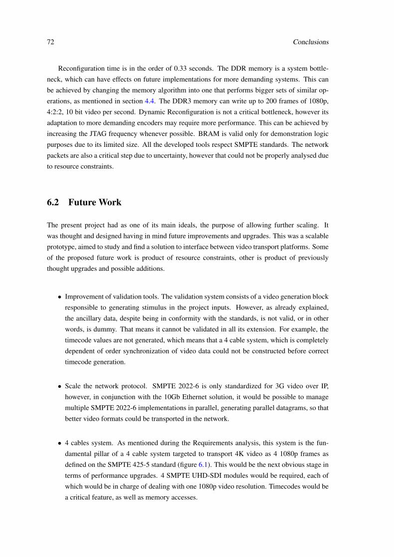
72 Conclusions
Reconfiguration time is in the order of 0.33 seconds. The DDR memory is a system bottle-
neck, which can have effects on future implementations for more demanding systems. This can
be achieved by changing the memory algorithm into one that performs bigger sets of similar op-
erations, as mentioned in section 4.4. The DDR3 memory can write up to 200 frames of 1080p,
4:2:2, 10 bit video per second. Dynamic Reconfiguration is not a critical bottleneck, however its
adaptation to more demanding encoders may require more performance. This can be achieved by
increasing the JTAG frequency whenever possible. BRAM is valid only for demonstration logic
purposes due to its limited size. All the developed tools respect SMPTE standards. The network
packets are also a critical step due to uncertainty, however that could not be properly analysed due
to resource constraints.
6.2 Future Work
The present project had as one of its main ideals, the purpose of allowing further scaling. It
was thought and designed having in mind future improvements and upgrades. This was a scalable
prototype, aimed to study and find a solution to interface between video transport platforms. Some
of the proposed future work is product of resource constraints, other is product of previously
thought upgrades and possible additions.
• Improvement of validation tools. The validation system consists of a video generation block
responsible to generating stimulus in the project inputs. However, as already explained,
the ancillary data, despite being in conformity with the standards, is not valid, or in other
words, is dummy. That means it cannot be validated in all its extension. For example, the
timecode values are not generated, which means that a 4 cable system, which is completely
dependent of order synchronization of video data could not be constructed before correct
timecode generation.
• Scale the network protocol. SMPTE 2022-6 is only standardized for 3G video over IP,
however, in conjunction with the 10Gb Ethernet solution, it would be possible to manage
multiple SMPTE 2022-6 implementations in parallel, generating parallel datagrams, so that
better video formats could be transported in the network.
• 4 cables system. As mentioned during the Requirements analysis, this system is the fun-
damental pillar of a 4 cable system targeted to transport 4K video as 4 1080p frames as
defined on the SMPTE 425-5 standard (figure 6.1). This would be the next obvious stage in
terms of performance upgrades. 4 SMPTE UHD-SDI modules would be required, each of
which would be in charge of dealing with one 1080p video resolution. Timecodes would be
a critical feature, as well as memory accesses.
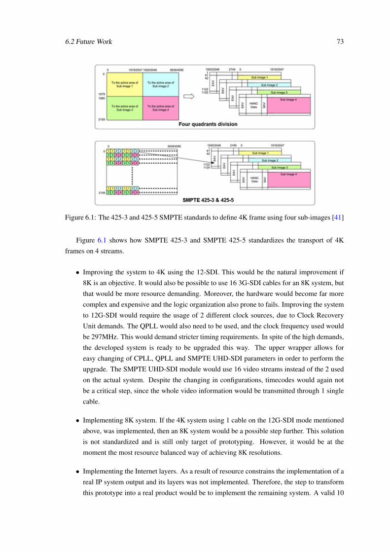
6.2 Future Work 73
Figure 6.1: The 425-3 and 425-5 SMPTE standards to define 4K frame using four sub-images [41]
Figure 6.1 shows how SMPTE 425-3 and SMPTE 425-5 standardizes the transport of 4K
frames on 4 streams.
• Improving the system to 4K using the 12-SDI. This would be the natural improvement if
8K is an objective. It would also be possible to use 16 3G-SDI cables for an 8K system, but
that would be more resource demanding. Moreover, the hardware would become far more
complex and expensive and the logic organization also prone to fails. Improving the system
to 12G-SDI would require the usage of 2 different clock sources, due to Clock Recovery
Unit demands. The QPLL would also need to be used, and the clock frequency used would
be 297MHz. This would demand stricter timing requirements. In spite of the high demands,
the developed system is ready to be upgraded this way. The upper wrapper allows for
easy changing of CPLL, QPLL and SMPTE UHD-SDI parameters in order to perform the
upgrade. The SMPTE UHD-SDI module would use 16 video streams instead of the 2 used
on the actual system. Despite the changing in configurations, timecodes would again not
be a critical step, since the whole video information would be transmitted through 1 single
cable.
• Implementing 8K system. If the 4K system using 1 cable on the 12G-SDI mode mentioned
above, was implemented, then an 8K system would be a possible step further. This solution
is not standardized and is still only target of prototyping. However, it would be at the
moment the most resource balanced way of achieving 8K resolutions.
• Implementing the Internet layers. As a result of resource constrains the implementation of a
real IP system output and its layers was not implemented. Therefore, the step to transform
this prototype into a real product would be to implement the remaining system. A valid 10
74 Conclusions
Gb Ethernet solution was already analyzed and could be the base of a more complex internet
distribution dedicated system.
• Forward Error Correction (FEC). The developed system incorporates CRC techniques that
allow the SMPTE UHD-SDI Receiver to identify if there were video transmission errors
during SDI transmission. However, the change of platforms from SDI to IP brings out a
different kind of data losses. Despite network packet loss, which is properly identified by
the RTP protocol, packet corruption can also be a problem. Therefore, the Forward Error
Correction algorithm can be applied to endure video network packets reliability. It is also
described on the SMPTE 2022-6 standard.
• Dynamic Partial Reconfiguration. The next step related to dynamic partial reconfiguration
is to implement an automatic system capable of loading the bitstreams when an event is
triggered.
References
[1] Jeremy G. Butler. Television: Critical Methods and Applications. Taylor & Francis, 2006,2006.
[2] Consumer Electronics Association (CEA). The Future is Clear – 4K Ultra High-DefinitionContinues to Build Positive Momentum, January 2015.
[3] Adam Flomenbaum. New research highlights rapid growth of 4kTV sales, cord-cutting households, 2015. [Online; accessed June24, 2016]. URL: http://www.thedrum.com/news/2015/10/15/new-research-highlights-rapid-growth-4k-tv-sales-cord-cutting-households.
[4] Charles Poynton. Digital Video and HDTV Algorithms and Interfaces. Number 1-55860-792-7. Morgan Kaufmann Publishers, 2003.
[5] John Hudson and Nigel Seth-Smith. 3G – The evolution of the Serial Digital Interface (SDI),January 2006.
[6] ADT Security Systems. Networked Video (Video Over IP) Benefits: A Guide for Small- toMedium-Sized Businesses. Technical report, ADT Security Systems, 2009.
[7] EBU UER. Advice on the use of 3 Gbit/s HD-SDI interfaces. (Technical Report 002), July2011.
[8] Richard F. Zarr. 4K Video: The Next Revolution. June 2014. [Online;accessed June 24, 2016]. URL: http://electronicdesign.com/embedded/4k-video-next-revolution.
[9] Xilinx. Video over IP. [Online; accessed June 24, 2016]. URL: http://www.xilinx.com/applications/broadcast/video-over-ip.html.
[10] Jeawoo Kim Hyun, Sangjin. Implementation of real time 4K S3D/8K UHD Capture system.
[11] M. Mitchell Waldrop. The chips are down for Moore’s law, February 2016.[Online; accessed June 24, 2016]. URL: http://www.nature.com/news/the-chips-are-down-for-moore-s-law-1.19338.
[12] Ilkka Tuomi. The Lives and Death of Moore’s Law. (Volume 7, Number 11), Novem-ber 2002. [Online; accessed June 24, 2016]. URL: http://firstmonday.org/ojs/index.php/fm/article/view/1000/921.
[13] Farzin Piltan. Research of Full Digital Control for Nonlinear Systems (e.g., Industrial RobotManipulator, IC Engine, Continuum Robot, and Spherical Motor) for Experimental Researchand Education Investor. Technical report, Iranian Institute of advanced science and Technol-ogy (IRAN SSP), 2012.
75
76 REFERENCES
[14] Louis Frenzel. Handbook of Serial Communications Interfaces: A Comprehensive Com-pendium of Serial Digital Input/Output (I/O) Standards. Newnes, 2015.
[15] SMPTE. Payload Identification Codes for Serial Digital Interfaces. (SMPTE ST 352-2010),March 2011.
[16] Wikipedia, the free encyclopedia. 8K UHD, 4K SHD, FHD and SD, 2015. [Online; accessedJune 24, 2016]. URL: https://commons.wikimedia.org/wiki/File:8K,_4K,_2K,_UHD,_HD.png.
[17] Chroma subsampling, 2015. [Online; accessed June 24,2016]. URL: http://calendar.perfplanet.com/2015/why-arent-your-images-using-chroma-subsampling/.
[18] Charles S. Swartz. Understanding Digital Cinema: A Professional Handbook. Taylor &Francis, 2004.
[19] Makarand Tapaswi. Why the RGB to YCbCr, July 2009. [Online; accessed June24, 2016]. URL: https://makarandtapaswi.wordpress.com/2009/07/20/why-the-rgb-to-ycbcr/.
[20] SMPTE. UHDTV Ecosystem Study Group Report. March 2014.
[21] SMPTE. 3 Gb/s Signal/Data Serial Interface. (SMPTE 424M-2006), April 2006.
[22] Tektronix. Broadcast Data Analysis. 2011.
[23] Xilinx. Zynq-7000 AP SoC and 7 Series Devices Memory Interface Solutions v2.4. Techni-cal Report WP-01055-1.0, Xilinx, March 2008.
[24] DDR comparison, 2004. [Online; accessed June 24, 2016]. URL: http://www.xbitlabs.com/articles/memory/display/ddr2_4.html.
[25] Xilinx. SMPTE UHD-SDI v1.0. (PG205), April 2015.
[26] Young Engineering. A-Law/Mu-Law Companding. (Revision 1.0), May 2003.
[27] Ralf Neuhaus. A Beginner’s Guide to Ethernet 802.3. (EE-269), June 2005.
[28] Industrial Ethernet Book. 10GbE relationship to OSI layer model, 2016. [Online; ac-cessed June 24, 2016]. URL: http://www.iebmedia.com/ethernet.php?id=5488&parentid=74&themeid=255&hft=39&showdetail=true&bb=1.
[29] Xilinx. XAUI v12.1. (PG053), November 2014.
[30] Agilent Technologies. 10 Gigabit Ethernet and the XAUI interface. Technical report, AgilentTechnologies, 2002.
[31] Marco D. Santambrogio et al Hsiung, Pao-Ann. Reconfigurable System Design and Verifica-tion. Number 9781420062670. Springer Science & Business Media, 2010.
[32] Video resolutions, 2014. [Online; accessed June 24, 2016]. URL: https://www.todoespacoonline.com/post.php?id=2745.
REFERENCES 77
[33] Xilinx. Xilinx Virtex-7 FPGA VC7203 Characterization Kit, 2014. [Online; accessedJune 24, 2016]. URL: http://www.xilinx.com/products/boards-and-kits/ck-v7-vc7203-g.html.
[34] Xilinx. Zynq-7000 AP SoC and 7 Series Devices Memory Interface Solutions v4.0.(UG586), June 2016.
[35] SMPTE. SMPTE Standards Update Webcast: Video Over IP Using The SMPTE 2022 Stan-dards, June 2013. [Online; accessed June 24, 2016]. URL: https://www.youtube.com/watch?v=ZtQdAvwSe1E.
[36] SMPTE. Transport of High Bit Rate Media Signals over IP Networks (HBRMT). (SMPTEST 2022-6:2012), October 2012.
[37] Xilinx. Implementing SMPTE SDI Interfaces with 7 Series GTX Transceivers. (XAP1249(v1.1), August 2015.
[38] Xilinx. Virtex-7 FPGA VC7203 Characterization Kit IBERT. (UG847 (v8.0)), October2014.
[39] Xilinx. VC7203 Virtex-7 FPGA GTX Transceiver Characterization Board. (UG957 (v1.3)),October 2014.
[40] Xilinx. Partial Reconfiguration. (UG947 (v2014.3)), October 2014.
[41] SMPTE. SMPTE 425-3 & SMPTE 425-5, June 2014. [Online; accessedJune 24, 2016]. URL: http://www.deltacast.tv/news/news/2014/deltacast-early-adopts-smpte-425-3-and-smpte-425-5-standards-for-4k-video.