
Study on buffer usage and data packing at the FE Federico Alessio, with inputs from Richard, Ken,...
38
Study on buffer usage and data packing at the FE Federico Alessio, with inputs from Richard, Ken, Guillaume LHCb Electronics Upgrade Meeting 11 April 2013
-
Upload
gerald-gallagher -
Category
Documents
-
view
217 -
download
0
Transcript of Study on buffer usage and data packing at the FE Federico Alessio, with inputs from Richard, Ken,...

Study on buffer usage and data packing at the FE
Federico Alessio, with inputs from Richard, Ken, Guillaume
LHCb Electronics Upgrade Meeting11 April 2013

LHCb Electronics Upgrade Meeting, 11/04/13 F. Alessio 2
Scope
Attempt to study: Impact of TFC commands on behaviour of FE buffer in
upgraded readout architecture Feasibility of packing algorithm across GBT link as specified
in readout architecture specifications
This presentation is NOT intended to show you how to pack across the GBT link or how to use the buffer. However, it IS intended to stimulate discussions using a practical example on possible solutions/implications at FE in the global readout architecture.
There is a published internal note which contains what I’m presenting here: LHCb-INT-2013-015 . It is not final, it is meant only to stimulate discussions feedbacks!

LHCb Electronics Upgrade Meeting, 11/04/13 F. Alessio 3
TFC simulation testbench
First simulation testbench (est. 2009) developed in VisualElite from Mentor Graphics. Includes:
• S-ODIN • SOL40 (only TFC) • LHC clock• LHC filling scheme• LLT emulation (based on current L0)• Custom-made FE emulation block
Generic FE emulation OT-like CALO-like
• No TELL40 emulation, throttle is faked • Everything is an HDL entity, portable to other simulation platforms
Basically, the aim is to simulate a (very small) slice of the readout system === Mini-DAQ including FE emulation• Could add few FE channels with different occupancies• *only problem is simulation time

LHCb Electronics Upgrade Meeting, 11/04/13 F. Alessio 4
(Simplified) TFC simulation testbench
S-ODIN Master logic
Emulated Control System
D
THROTTLE TFC
D
TELL40 emulation
Simplified Readout Logic
TFC Encoder/Decoder
Block
FE emulation
FE Logic
EMULATED DATA(programmable delay/distance)
TFCTHROTTLE
S-ODIN HDL code
Clock generators
40 MHz Clock
Orbit Clock
Filling Scheme emulator
SOL40 Fan-out/Fan-in logic
Emulated Control System
SOL40 HDL code
THROTTLE
TFC
L0 logic
LLT emulation
LLT
TFC
TFC
Emulation
Synthesizable

LHCb Electronics Upgrade Meeting, 11/04/13 F. Alessio 5
FE emulation, why?
Needed to develop a FE emulation block to simulate the generation of detector data
Used to • study impact of TFC commands at FE buffer behaviour• demonstrate feasibility of packing mechanism at FE as written in specs• emulate FE data generator to spy on sub-detectors for FE reviews….
Proposed to use it as a practical example of a generic FE data generator for the readout architecture simulation framework until sub-detectors’ codes become available
• Description of the code here• Simulation results• Considerations on packing mechanism• Considerations on buffer usage• Synthesis results
Practical proof of how important simulating code is…

LHCb Electronics Upgrade Meeting, 11/04/13 F. Alessio 6
Generic FE channel as in specs
FE channel contains a buffer: No trigger at FE, so buffer is actually a
derandomizer. Used to pipe data @ 40MHz to be
packed and sent over GBT link. If no TFC command and occupancy too
high, buffer will fill up very very quickly• We are running at 40MHz! It’s 40
times faster than now… • Mechanism to empty buffer• TFC commands come in handy
DATA coming out on GBT link:• No empty spaces, no unexpected 0s• Fully dynamic packing algorithm across
GBT frame-width• Wishingly, data should be in order…

LHCb Electronics Upgrade Meeting, 11/04/13 F. Alessio 7
The code: FE data generator
DERANDOMIZING BUFFERProgrammable Depth
Width: (number of channels * channel size) + header size
CHANNEL DATA GENERATOR
DATA OCCUPANCY GENERATOR
(POISSON)
LHC MACHINE (FILLING SCHEME)
DATA WORD(number of channels * channel size)
EVENT HEADER( 12 bits BCLK identifier
+ 4 status bits + 8 bits for data size )
ELSE
IF DATA_SIZE = 0 (no hit)or BX_VETO = 1
or HEADER_ONLY = 1
DO NOT WRITE TO DERANDOMIZER WHILE PACKING JUST HEADERS!à RECUPERATE BUFFER SPACE
à FORCE DATA SIZE TO 0 IN HEADER FOR TELL40 DECODINGà MAX # OF HEADERS IN WORD =
ROUND_TO_INT(GBT WORD SIZE / HEADER SIZE)
GBT PACKING LOGIC
GBT FRAME – EXAMPLE WITH GBT SIZE 84 BITS WITH FEC CORRECTION
IF NZS_MODE = 1 occupancy 100%
à put all channels in word
WRITE TO DERANDOMIZER
Padded to 0s... EVENT HEADER
EVENT HEADER
EVENT HEADER
...
0x5 NB: GBT HEADER = X”5” if data or X”6" if IDLEEV 01 HEADERDATA WORD of EV 01
0x5EV 02 HEADER REST OF DATA WORD of EV 01 DW of EV 02
0x5REST OF DATA WORD of EV 02
0x5REST OF EV 04
HEADER
EX: EV02 is NZS
0x5REST OF DATA WORD of EV 02
0x5REST OF DATA WORD of EV 02
FOLLOWING 3 EVENTS HAVE HEADER ONLY = 1 FROM TFC
EV 05 HEADEREV 06 HEADERDW OF EV 06
0x5REST OF DATA WORD of EV 06 NEXT EVENT IS IN LINE
0x5EV 07 HEADER REST OF DATA WORD of EV 06 DW of EV 07
0x5EV 08 HEADER REST OF DATA WORD of EV 07 DW of EV 08
0x5REST OF DATA WORD of EV 08
0x5
EV 09 HEADER
DATA WORD of EV 09
.
.
.GBT ENCODER
IF FE_RESET = 1 or SYNCH = 1
à reset derandomizer buffer
0x5EV XX HEADER00000MANUAL ALIGNMENT FRAME
(programmable via ECS)
.
.
.
This part should be replaced by sub-detector’s specific data generated from MonteCarlo simulation
NB: data word width can include other informationà e.g. width would be (number_of_channels *
channel_size) + hit_pattern_size (== number_of_channels)
0x600000DERANDOMIZER IS EMPTY, SEND IDLE
FRAME OVER GBT FRAME
0x5... TWO EMPTY EVENTS
DERANDOMIZER ALMOST FULL
à leaving some buffer space for safety margin
SYNCH will always follow a FE RESET in order to achieve link synchronizationà during SYNCH command asserted, FE should exchange data field with MANUAL
ALIGNMENT FRAME for links synchronization
0x5EV XX+1 HEADER
00000MANUAL ALIGNMENT FRAME
(programmable via ECS)
READ FROM DERANDOMIZER
FIXED OR DYNAMIC LATENCY,
Not implemented and sub-detector specific
SUPPRESSION / COMPRESSION
MECHANISM
DO NOT WRITE TO DERANDOMIZER WHILE PACKING JUST HEADERS!à RECUPERATE BUFFER SPACE
à SET TRUNCATED BIT = 1à MAX # OF HEADERS IN WORD =
ROUND_TO_INT(GBT WORD SIZE / HEADER SIZE)
Padded to 0s... EVENT HEADER
EVENT HEADER
EVENT HEADER
...
EV 03 HEADEREV 04
HEADER
GBT ENCODER
ELSE
EV 10 HEADEREV 11
HEADER
REST of EV 11 HEADER
LHCb Electronics Upgrade Meeting, 11/04/13 F. Alessio 8
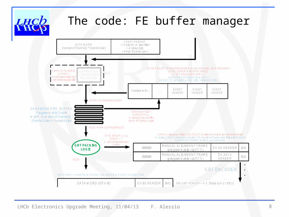
The code: FE buffer manager
DERANDOMIZING BUFFERProgrammable Depth
Width: (number of channels * channel size) + header size
CHANNEL DATA GENERATOR
DATA OCCUPANCY GENERATOR
(POISSON)
LHC MACHINE (FILLING SCHEME)
DATA WORD(number of channels * channel size)
EVENT HEADER( 12 bits BCLK identifier
+ 4 status bits + 8 bits for data size )
ELSE
IF DATA_SIZE = 0 (no hit)or BX_VETO = 1
or HEADER_ONLY = 1
DO NOT WRITE TO DERANDOMIZER WHILE PACKING JUST HEADERS!à RECUPERATE BUFFER SPACE
à FORCE DATA SIZE TO 0 IN HEADER FOR TELL40 DECODINGà MAX # OF HEADERS IN WORD =
ROUND_TO_INT(GBT WORD SIZE / HEADER SIZE)
GBT PACKING LOGIC
GBT FRAME – EXAMPLE WITH GBT SIZE 84 BITS WITH FEC CORRECTION
IF NZS_MODE = 1 occupancy 100%
à put all channels in word
WRITE TO DERANDOMIZER
Padded to 0s... EVENT HEADER
EVENT HEADER
EVENT HEADER
...
0x5 NB: GBT HEADER = X”5” if data or X”6" if IDLEEV 01 HEADERDATA WORD of EV 01
0x5EV 02 HEADER REST OF DATA WORD of EV 01 DW of EV 02
0x5REST OF DATA WORD of EV 02
0x5REST OF EV 04
HEADER
EX: EV02 is NZS
0x5REST OF DATA WORD of EV 02
0x5REST OF DATA WORD of EV 02
FOLLOWING 3 EVENTS HAVE HEADER ONLY = 1 FROM TFC
EV 05 HEADEREV 06 HEADERDW OF EV 06
0x5REST OF DATA WORD of EV 06 NEXT EVENT IS IN LINE
0x5EV 07 HEADER REST OF DATA WORD of EV 06 DW of EV 07
0x5EV 08 HEADER REST OF DATA WORD of EV 07 DW of EV 08
0x5REST OF DATA WORD of EV 08
0x5
EV 09 HEADER
DATA WORD of EV 09
.
.
.GBT ENCODER
IF FE_RESET = 1 or SYNCH = 1
à reset derandomizer buffer
0x5EV XX HEADER00000MANUAL ALIGNMENT FRAME
(programmable via ECS)
.
.
.
This part should be replaced by sub-detector’s specific data generated from MonteCarlo simulation
NB: data word width can include other informationà e.g. width would be (number_of_channels *
channel_size) + hit_pattern_size (== number_of_channels)
0x600000 DERANDOMIZER IS EMPTY, SEND IDLE FRAME OVER GBT FRAME
0x5... TWO EMPTY EVENTS
DERANDOMIZER ALMOST FULL
à leaving some buffer space for safety margin
SYNCH will always follow a FE RESET in order to achieve link synchronizationà during SYNCH command asserted, FE should exchange data field with MANUAL
ALIGNMENT FRAME for links synchronization
0x5EV XX+1 HEADER
00000MANUAL ALIGNMENT FRAME
(programmable via ECS)
READ FROM DERANDOMIZER
FIXED OR DYNAMIC LATENCY,
Not implemented and sub-detector specific
SUPPRESSION / COMPRESSION
MECHANISM
DO NOT WRITE TO DERANDOMIZER WHILE PACKING JUST HEADERS!à RECUPERATE BUFFER SPACE
à SET TRUNCATED BIT = 1à MAX # OF HEADERS IN WORD =
ROUND_TO_INT(GBT WORD SIZE / HEADER SIZE)
Padded to 0s... EVENT HEADER
EVENT HEADER
EVENT HEADER
...
EV 03 HEADEREV 04
HEADER
GBT ENCODER
ELSE
EV 10 HEADEREV 11
HEADER
REST of EV 11 HEADER

LHCb Electronics Upgrade Meeting, 11/04/13 F. Alessio 9
The code: GBT dynamic packing DERANDOMIZING BUFFERProgrammable Depth
Width: (number of channels * channel size) + header size
CHANNEL DATA GENERATOR
DATA OCCUPANCY GENERATOR (POISSON)
LHC MACHINE (FILLING SCHEME)
DATA WORD(number of channels * channel size)
EVENT HEADER( 12 bits BCLK identifier
+ 4 status bits + 8 bits for data size )
ELSE
IF DATA_SIZE = 0 (no hit)or BX_VETO = 1
or HEADER_ONLY = 1
DO NOT WRITE TO DERANDOMIZER WHILE PACKING JUST HEADERS!à RECUPERATE BUFFER SPACE
à FORCE DATA SIZE TO 0 IN HEADER FOR TELL40 DECODINGà MAX # OF HEADERS IN WORD =
ROUND_TO_INT(GBT WORD SIZE / HEADER SIZE)
GBT PACKING LOGIC
GBT FRAME – EXAMPLE WITH GBT SIZE 84 BITS WITH FEC CORRECTION
IF NZS_MODE = 1 occupancy 100%
à put all channels in word
WRITE TO DERANDOMIZER
Padded to 0s... EVENT HEADER
EVENT HEADER
EVENT HEADER
...
0x5 NB: GBT HEADER = X”5” if data or X”6" if IDLEEV 01 HEADERDATA WORD of EV 01
0x5EV 02 HEADER REST OF DATA WORD of EV 01 DW of EV 02
0x5REST OF DATA WORD of EV 02
0x5REST OF EV 04
HEADER
EX: EV02 is NZS
0x5REST OF DATA WORD of EV 02
0x5REST OF DATA WORD of EV 02
FOLLOWING 3 EVENTS HAVE HEADER ONLY = 1 FROM TFC
EV 05 HEADEREV 06 HEADERDW OF EV 06
0x5REST OF DATA WORD of EV 06 NEXT EVENT IS IN LINE
0x5EV 07 HEADER REST OF DATA WORD of EV 06 DW of EV 07
0x5EV 08 HEADER REST OF DATA WORD of EV 07 DW of EV 08
0x5REST OF DATA WORD of EV 08
0x5
EV 09 HEADER
DATA WORD of EV 09
.
.
.GBT ENCODER
IF FE_RESET = 1 or SYNCH = 1
à reset derandomizer buffer
0x5EV XX HEADER00000MANUAL ALIGNMENT FRAME
(programmable via ECS)
.
.
.
This part should be replaced by sub-detector’s specific data generated from MonteCarlo simulation
NB: data word width can include other informationà e.g. width would be (number_of_channels *
channel_size) + hit_pattern_size (== number_of_channels)
0x600000 DERANDOMIZER IS EMPTY, SEND IDLE FRAME OVER GBT FRAME
0x5... TWO EMPTY EVENTS
DERANDOMIZER ALMOST FULL
à leaving some buffer space for safety margin
SYNCH will always follow a FE RESET in order to achieve link synchronizationà during SYNCH command asserted, FE should exchange data field with MANUAL
ALIGNMENT FRAME for links synchronization
0x5EV XX+1 HEADER
00000MANUAL ALIGNMENT FRAME
(programmable via ECS)
READ FROM DERANDOMIZER
FIXED OR DYNAMIC LATENCY,
Not implemented and sub-detector specific
SUPPRESSION / COMPRESSION
MECHANISM
DO NOT WRITE TO DERANDOMIZER WHILE PACKING JUST HEADERS!à RECUPERATE BUFFER SPACE
à SET TRUNCATED BIT = 1à MAX # OF HEADERS IN WORD =
ROUND_TO_INT(GBT WORD SIZE / HEADER SIZE)
Padded to 0s... EVENT HEADER
EVENT HEADER
EVENT HEADER
...
EV 03 HEADEREV 04
HEADER
GBT ENCODER
ELSE
EV 10 HEADEREV 11
HEADER
REST of EV 11 HEADER
Very important to analyze simulation
output bit-by-bit and clock-by-clock!

LHCb Electronics Upgrade Meeting, 11/04/13 F. Alessio 10
FE generic data generator is fully programmable: Number of channels associated to GBT link Width of each channel Derandomizer depth Mean occupancy of the channels associated to GBT link Size of GBT frame (80 bits or WideBus + GBT header 4 bits)
Extremely flexible and easy to configure with parameters
Covers almost all possibilities (almost…) Including flexible transmission of NZS and ZS
Including TFC commands as defined in specs Study dependency of FE buffer behaviour with TFC commands Study effect of packing algorithm on TELL40 Study synchronization mechanism at beginning of run Study re-synchronization mechanism when de-synchronized Etc… etc… etc…
And it is fully synthesizable…
The code: configuration
LHCb Electronics Upgrade Meeting, 11/04/13 F. Alessio 11
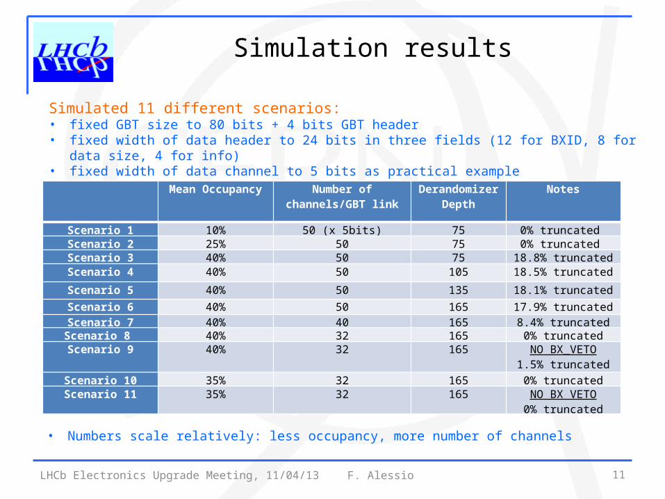
Simulated 11 different scenarios:• fixed GBT size to 80 bits + 4 bits GBT header• fixed width of data header to 24 bits in three fields (12 for BXID, 8 for data size, 4 for
info)• fixed width of data channel to 5 bits as practical example
Mean Occupancy Number of channels/GBT link
Derandomizer Depth
Notes
Scenario 1 10% 50 (x 5bits) 75 0% truncated Scenario 2 25% 50 75 0% truncated Scenario 3 40% 50 75 18.8% truncatedScenario 4 40% 50 105 18.5% truncated
Scenario 5 40% 50 135 18.1% truncatedScenario 6 40% 50 165 17.9% truncatedScenario 7 40% 40 165 8.4% truncatedScenario 8 40% 32 165 0% truncatedScenario 9 40% 32 165 NO BX_VETO
1.5% truncated
Scenario 10 35% 32 165 0% truncatedScenario 11 35% 32 165 NO BX VETO
0% truncated
Simulation results
• Numbers scale relatively: less occupancy, more number of channels

LHCb Electronics Upgrade Meeting, 11/04/13 F. Alessio 12
Scenario 1: 10% occupancy, 50x5bits channels, derandomizer depth 75
Scenario 2: 25% occupancy, 50x5bits channels, derandomizer depth 75
Simulation results
LHCb Electronics Upgrade Meeting, 11/04/13 F. Alessio 13
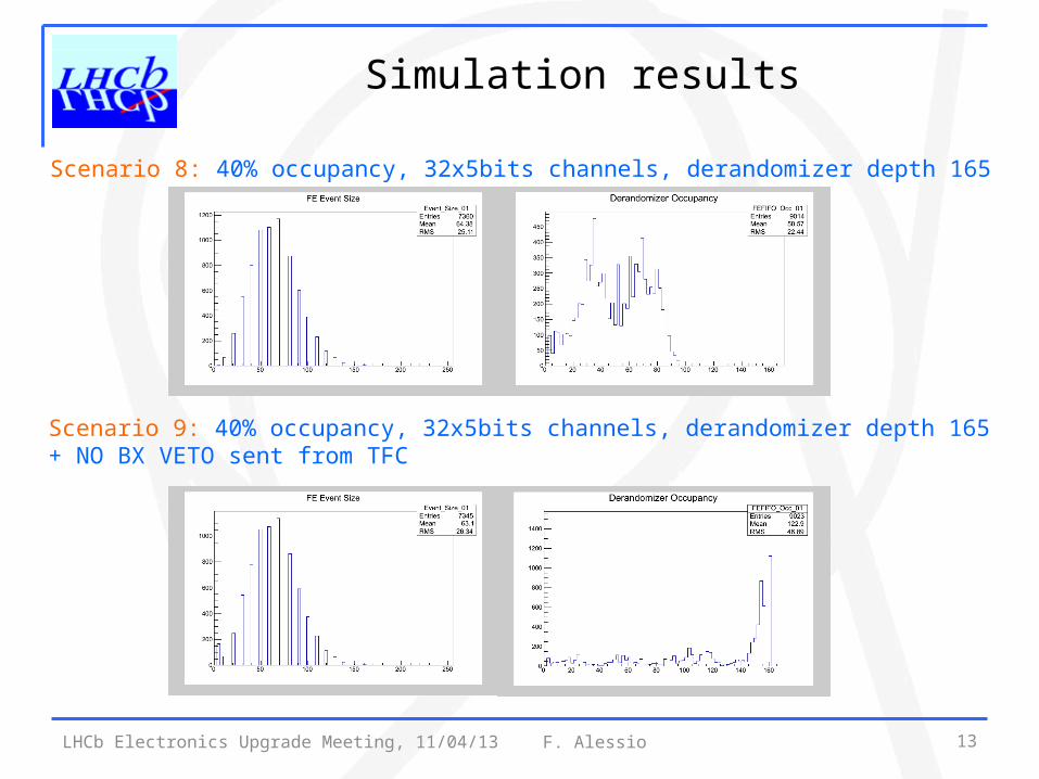
Scenario 8: 40% occupancy, 32x5bits channels, derandomizer depth 165
Scenario 9: 40% occupancy, 32x5bits channels, derandomizer depth 165 + NO BX VETO sent from TFC
Simulation results

LHCb Electronics Upgrade Meeting, 11/04/13 F. Alessio 14
For a bit-by-bit zoom in please come to my office
Filling scheme
TFC commands
GBT output
Derandomizer occupancy
FE data generated
Simulation results

LHCb Electronics Upgrade Meeting, 11/04/13 F. Alessio 15
For a bit-by-bit zoom in please come to my office or ask the code
Simulation results

LHCb Electronics Upgrade Meeting, 11/04/13 F. Alessio 16
Synthesis results
Stratix IV GX 230KF40C Resource
Usage
Estimated ALUTs Used 3228 (<2% Total)Dedicated logic registers 896 (<1% Total)Memory ALUTs Used 0 (0% Total)Estimated ALUTs Unavailable 719Total combinatorial functions 3228 7 input functions 18 6 input functions 947 5 input functions 379 4 input functions 430 <= 3 input functions 1454Combinatorial ALUTs by mode normal mode 2904 extended LUT mode 18 arithmetic mode 274 shared arithmetic mode 32Total registers 896 (no I/Os)Clock speed Fmax registered (only main clock)
172.71 MHz
ARRIA GX 35DF78 Resource
Usage
Estimated ALUTs Used 2636 (10% Total)Dedicated logic registers 846 (3% Total)Memory ALUTs Used 0 (0% Total)Estimated ALUTs Unavailable 457Total combinatorial functions 2635 7 input functions 17 6 input functions 895 5 input functions 387 4 input functions 252 <= 3 input functions 1084Combinatorial ALUTs by mode normal mode 2312 extended LUT mode 17 arithmetic mode 274 shared arithmetic mode 32Total registers 896 (no I/Os)
• Using Quartus Altera 12.1 SP1 • No synthesis optimization done, let fitter free, no pinout defined, no timing
constraint• No memory cells used• Doable, can be further improved though.

LHCb Electronics Upgrade Meeting, 11/04/13 F. Alessio 17
Simulation should be a coordinated effort Personal drive in order to be able to produce a (complex) code for TFC on time
FE generic code + TFC code should be merged with TELL40 effort To test both FE packing algorithm and FE buffer management To test decoding at TELL40 and investigate consequences/solutions To analyze effects of TFC commands on global system (including TELL40)
• Effort already ongoing between me and Guillaume to do so
We would very very much appreciate to have the code (emulation) of each sub-detectors a FE generic code is useful to study things on paper, but real code is
something different
Proposal is to use this simulation effort to validate FE code simulation performed by me and Guillaume to investigate solutions, issues in
FE
FYI, simulation outlook

LHCb Electronics Upgrade Meeting, 11/04/13 F. Alessio 18
Packing mechanism as specified in our document is feasible. Will be used temporarily to emulate FE generated data in global readout
and TFC simulation.
However, very big open questions: Is your FE compatible with such scheme? What about such code in an
ASIC?
Behaviour of FE derandomizer will strongly depend on your compression or suppression mechanism.
• If dynamic could create big latencies• If your data does not come out of order can become quite
complicated…
Behaviour of FE derandomizer will strongly depend on TFC commands• FE buffer depth should not rely on having a BX VETO! Aim at a
bandwidth for fully 40 MHz readout BX VETO solely to discard events synchronously.
• What about SYNCH command? When do you think you can apply it? Ideally after derandomizer and after suppression/compression, but…
How many clock cycles do you need to recover from an NZS event?• Can you handle consecutive NZS events?
Conclusions

LHCb Electronics Upgrade Meeting, 11/04/13 F. Alessio 19
Qs & As?

LHCb Electronics Upgrade Meeting, 11/04/13 F. Alessio 20
System and functional requirements
1. Bidirectional communication network
2. Clock jitter, and phase and latency control
At the FE, but also at TELL40 and between S-TFC boards
3. Partitioning to allow running with any ensemble and parallel partitions
4. LHC interfaces
5. Events rate control
6. Low-Level-Trigger input
7. Support for old TTC-based distribution system
8. Destination control for the event packets
9. Sub-detectors calibration triggers
10.S-ODIN data bank
Infomation about transmitted events
11.Test-bench support
LHCb Electronics Upgrade Meeting, 11/04/13 F. Alessio
Readout Supervisor
S-ODIN
Interface boardsSOL40
Readout BoardsTELL40s
Front-Ends
LHC Interfaces
TFC
TFC + ECS
TFC
EFFECS (FE)
LLT
THROTTLEECS
40 Gb/s
2.4 Gb/s
4.8 Gb/s
2.4 Gb/s
10 Gb/s
2.4 Gb/s 40 MHz clock
21
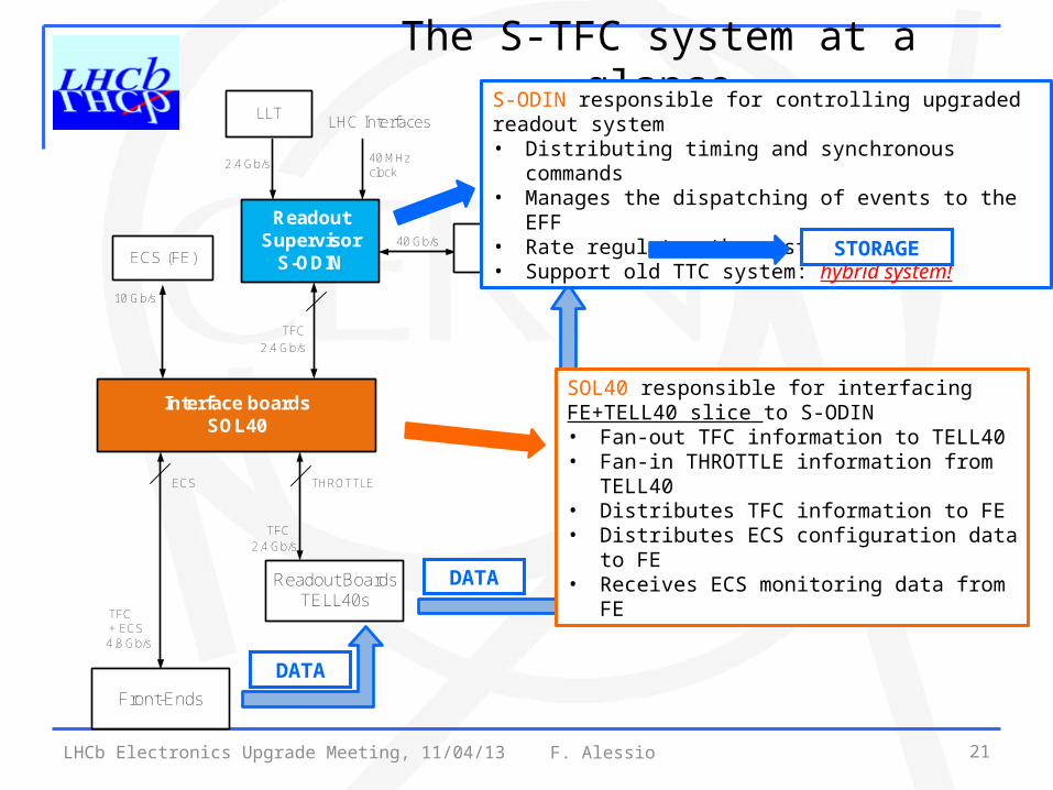
The S-TFC system at a glance
DATA
DATA
S-ODIN responsible for controlling upgraded readout system • Distributing timing and synchronous commands• Manages the dispatching of events to the EFF• Rate regulates the system• Support old TTC system: hybrid system!
SOL40 responsible for interfacing FE+TELL40 slice to S-ODIN• Fan-out TFC information to TELL40• Fan-in THROTTLE information from
TELL40• Distributes TFC information to FE • Distributes ECS configuration data to FE• Receives ECS monitoring data from FE
STORAGE

LHCb Electronics Upgrade Meeting, 11/04/13 F. Alessio
S-TFC concept reminder
22
LHC Interface
Clock Fanout
CLK
ECS
PH
Y
Programmable Switch layer (Partitioning)
Built-in GX Transceivers layer
PH
Y FARM
n
n
#links = #LHCb sub-systems
S-ODIN
TFC+ECS Interface
TF
C,
Th
rott
le
FAN-OUT/FAN-IN Logic
+ECS to FE
encoding Logic+
optional S-ODIN Logic
Switch Logic
Master FPGA (STRATIX IV/V GX)
S-ODIN Logic Instantiations (x6)
Master FPGA (STRATIX IV/V GX)
LLT
FE electronics
TELL40s
GB
T
FPGA-to-FPGA transceivers
S-ODIN Logic
PH
Y
ECS to FE

LHCb Electronics Upgrade Meeting, 11/04/13 F. Alessio
Readout Crate
Rea
do
ut
Bo
ard
s
FEs FEs FEs...FEs FEs FEs...FEs FEs FEs...
SO
L40
TFC on backplane
ECS
TFC Crate
S-O
DIN
, LL
T, L
HC
LHC clock, LHC interfaces
Tri
gg
er B
oar
ds
FARM
DATATFC+ECS
Rea
do
ut
Bo
ard
s
Rea
do
ut
Bo
ard
s
Rea
do
ut
Bo
ard
s
Rea
do
ut
Bo
ard
s
Rea
do
ut
Bo
ard
s
Rea
do
ut
Bo
ard
s
Rea
do
ut
Bo
ard
s
The upgraded physical readout slice
Common electronics board for upgraded readout system: Marseille’s ATCA board with 4 AMC cards
• S-ODIN AMC card• LLT AMC card• TELL40 AMC card• LHC Interfaces specific AMC card
23

LHCb Electronics Upgrade Meeting, 11/04/13 F. Alessio
Latest S-TFC protocol to TELL40
24
«Extended» TFC word to TELL40 via SOL40: 64 bits sent every 40 MHz = 2.56 Gb/s (on backplane) packed with 8b/10b protocol (i.e. total of 80 bits) no dedicated GBT buffer, use ALTERA GX simple 8b/10b
encoder/decoder
THROTTLE information from each TELL40 to SOL40: • no change: 1 bit for each AMC board + BXID for which the throttle was
set 16 bits in 8b/10b encoder same GX buffer as before (as same decoder!)
Constant latency after BXID
We will provide the TFC decoding block for the TELL40: VHDL entity with inputs/outputs
BXID(11..0) MEP Dest(31..0) Trigger Type(3..0) Calibration Type(3..0)
Trigger BX Veto NZS Mode
Header Only
BE Reset
BXID Reset
FE Reset
EID Reset
Synch Snapshot
Reserve
0123456789
13 .. 1017 .. 1449 .. 18505163 .. 52MEP
Accept
MEP accept command when MEP ready: Take MEP address and pack to FARM No need for special address, dynamic

LHCb Electronics Upgrade Meeting, 11/04/13 F. Alessio
S-TFC protocol to FE, no change
25
TFC word on downlink to FE via SOL40 embedded in GBT word: 24 bits in each GBT frame every 40 MHz = 0.98 Gb/s all commands associated to BXID in TFC word
Put local configurable delays for each TFC command • GBT does not support individual delays for each line• Need for «local» pipelining: detector delays+cables+operational logic (i.e. laser
pulse?) DATA SHOULD BE TAGGED WITH THE CROSSING TO WHICH IT BELONGS!
TFC word will arrive before the actual event takes place• To allow use of commands/resets for particular BXID• Accounting of delays in S-ODIN: for now, 16 clock cycles earlier + time to receive• Aligned to the furthest FE (simulation, then in situ calibration!)
TFC protocol to FE has implications on GBT configuration and ECS to/from FE• see specs document!
23 .. 12 11 10 9 8 .. 5 4 3 2 1 0
BXID(11..0) Synch NZS Mode
Header Only
BXID Reset
FE ResetCalibration Type(3..0) BX VetoSnapshotReserve

LHCb Electronics Upgrade Meeting, 11/04/13 F. Alessio 26
SODIN firmware v1r0 – block diagram
OR
BIT
BXID cnt BXIDBCLK
Internal Triggers
RndTrg Gen
PerTrg Gen
PerTrg Gen
CalibTrg Gen
CalibTrg Gen
CalibTrg Gen
CalibTrg Gen
BXID
RndTrgA
LumiTrgs
RndTrgC
RndTrgD
PerTrg01
PerTrg02
CalibTrgA
CalibTrgB
CalibTrgC
CalibTrgD
LLT INPUT LLT Trg
LLT Type
AUX INPUTAUX Trg
Trg Manager
FE reset handler
BE reset handler
FE RESET (from ECS)
BE RESET (from ECS)
Header Only TRG
BX Veto TRG
Trigger TRG
Trigger Type TRG
LLT Trg Enb
LLT Beamgas Enb
AUX Trg Enb
Calib Type TRG
Trigger BXID TRG
NZS/TAE handler
LLT BXID
BXID
NZ
S e
nb
NZ
S
con
secu
tive
NZ
S w
ait
EID RESET (from ECS)
EID reset handler
TA
E e
nb
FE Reset TRG (1 clock cycle)
BE Reset TRG (1 clock cycle)
Header Only TAE
BX Veto TAE
Calib Type TAE
Trigger BXID TAE
NZS mode TAE
Synch(from ECS)
Synch cmd
handler
Syn
ch Cm
d
MEP handler
FARM
ME
P w
ind
ow
MEP destination
TFC WORD (64bits in 8b/10b
encoder) ~2.5Gb/s
ME
P
des
tinat
ion
enb
Throttle handler
Throttle
Throttle BXID
BXID
S-ODIN Master Logic
SODIN data bank creator SODIN data bank to FARM
(12 x 32b Ethernet)~16Gb/s
ME
P d
estinatio
n
Trg BX Type TRG Trg BX Type TAE
UTC start time(from ECS)
UTC time++
OD
IN d
ata
ban
k e
nb
Throttle enb
BX Type Handler BX Type
WriteRead
Fill
ing
S
che
me
(f
rom
EC
S)
Filling Scheme RAM (224 x 32b)
EID cntEID accept
Run number (from ECS)
EID Reset TRG (1 clock cycle)
Synch Cmd TRG (2 or more clock cycles)
TCK (from ECS)
Snapshot(from ECS)
Snapshot cmd
handler
Synch length(from ECS)
Snapshot interval
(from ECS)
BX
ID R
ese
t
FE Reset TAE
BE Reset TAE
EID Reset TAE
Synch Cmd TAE
TA
E la
tenc
y co
mp
ens
atio
n
Trigger Type TAE
Trigger TAE
FE
Re
set wa
term
ark
FE
Re
set
BE
Re
set w
ate
rma
rk
BE
Re
set
EID
Re
set
Th
rottle
NZ
S+
TA
E
wa
term
ark
TA
E w
ind
ow
EID
Re
set
Sn
apsh
ot C
md
BXID reset handlerBXID
PA
US
E (fro
m E
CS
)
ME
P d
yna
mic
d
estin
atio
n en
b
MEP throttle
EID

LHCb Electronics Upgrade Meeting, 11/04/13 F. Alessio
Timing distribution
27
From TFC point of view, we ensure constant: LATENCY: Alignment with BXID FINE PHASE: Alignment with best sampling point
TELL40sTELL40s
Front-EndsFront-Ends
TFC+ECSInterfaceS-ODIN TELL40s
Front-Ends
LHC Clocks
= Receiver
= Transmitter
GBT for TFC+ECS GBT for
DATA
FE ASIC
FE ASIC
FE ASIC
Some resynchronization mechanisms envisaged: Within TFC boards With GBT
No impact on FE itself
Loopback mechanism: re-transmit TFC word
back allows for latency
measurement + monitoring of TFC commands and synchronization

LHCb Electronics Upgrade Meeting, 11/04/13 F. Alessio
DCS objectDCS
object
TELL40TELL40TELL40
GBTX SCA SCA
DCS object
GBTX GBTX GBTX GBTX GBTX GBTX
FE ASIC
FE ASIC
FE ASIC
FE ASIC
FE ASIC
24
DATA
TFC commands
SOL40
SCA
TFC+ECS GBT
DATA GBT
SCA SCA SCA Configuration data / monitoring data
I2C, JTAG…
Clock
TFC+ECS
Generic FE electronics architecture28
How to decode TFC in FE chips?
Use of TFC+ECS GBTs in FE is 100% common to everybody!! dashed lines indicate the detector
specific interface parts please pay particular care in the
clock transmission: the TFC clock must be used by FE to transmit data, i.e. low jitter!
Kapton cable, crate, copper between FE ASICs and GBTX
FE electronic block
LHCb Electronics Upgrade Meeting, 11/04/13 F. Alessio
FEModule
FEModule
Phase – Aligners + Ser/Des for E – Ports
FEModule
E – PortE – Port
E – Port
GBT – SCA
E – Port
Phase - Shifter
E – PortE – Port
E – PortE – Port
CDR
DEC/D
SCR
SER
SCR/ENC
I2C MasterI2C Slave
Control Logic Configuration(e-Fuses + reg-Bank)
Clock[7:0]
CLK Manager
CLK Reference/xPLL
External clock reference
clockscontroldata
one 80 Mb/s port
I2C port
I2C (light)
JTAG
80, 160 and 320 Mb/s ports
GBTIA
GBLD
GBTXe-Link
clock
data-up
data-down
ePLLTxePLLR
x
JTAG port
29
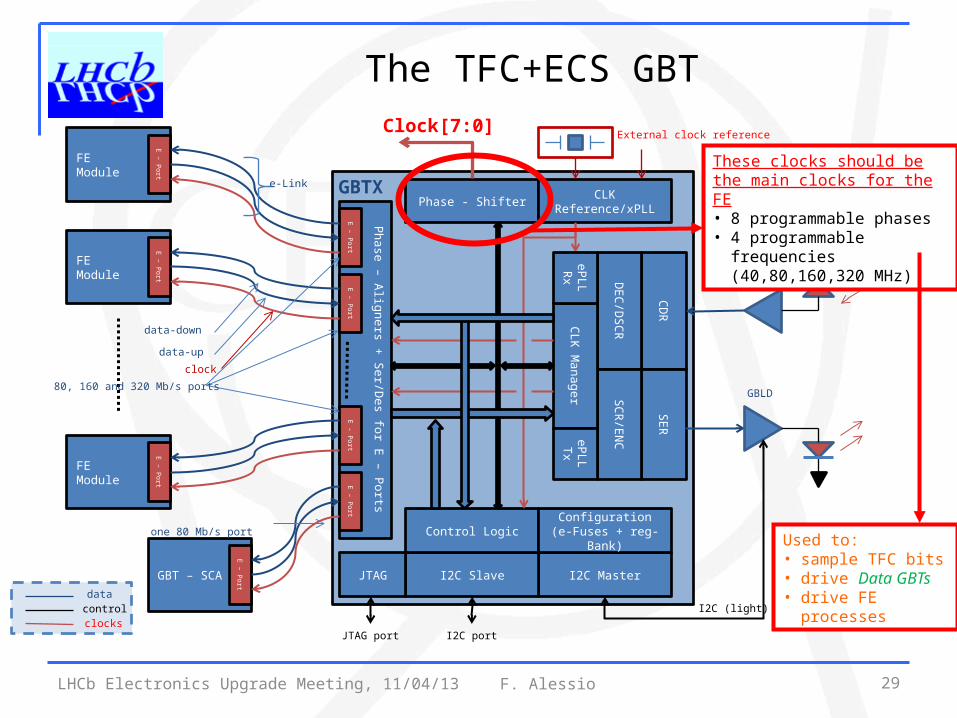
The TFC+ECS GBT
These clocks should be the main clocks for the FE• 8 programmable phases • 4 programmable
frequencies (40,80,160,320 MHz)
Used to:• sample TFC bits • drive Data GBTs • drive FE
processes
LHCb Electronics Upgrade Meeting, 11/04/13 F. Alessio 30
The TFC+ECS GBT protocol to FE
D0D1D2D3D4ECICHEADER FEC
GBT word: 120 bits
2x16 bits16bits2x2bits4bits
24 e-links @ 80 Mb/sfor TFC
Idle: 0110Data: 0101
1 e-link @ 80 Mb/s for
GBT internal use only 1 e-link @
80 Mb/s to GBT-SCA
SCA
16 e-link @ 80 Mb/s to 16 GBT-SCAs
for ECS
16bits16bits16bits16bits
SCAs SCAs
TFC protocol has direct implications in the way in which GBT should be used everywhere• 24 e-links @ 80 Mb/s dedicated to TFC word:
use 80 MHz phase shifter clock to sample TFC parallel word• TFC bits are packed in GBT frame so that they all come out on the same clock edge
We can repeat the TFC bits also on consecutive 80 MHz clock edge if needed
Leftover 17 e-links dedicated to GBT-SCAs for ECS configuring and monitoring (see later)

LHCb Electronics Upgrade Meeting, 11/04/13 F. Alessio 31
Words come out from GBT at 80 Mb/s
D0[14..2,0]D1D2D3D4EC[0]IC[0]H[2,0] FEC[30..6,4,2,0]
D0[15..3,1]D1D2D3D4EC[1]IC[1]H[3,1] FEC[31..7,5,3,1]
24bits x TFC à grouped e-link + 1
clock line
Other purposes?
17bits x ECSà 17 GBT-SCA
17bits x ECS msb first, odd bits
lsb second, even bits
In simple words:• Odd bits of GBT protocol on rising edge of 40 MHz clock (first, msb), • Even bits of GBT protocol on falling edge of 40 MHz clock (second,
lsb)

LHCb Electronics Upgrade Meeting, 11/04/13 F. Alessio 32
TFC decoding at FE after GBT
D0[1] D0[0] D0[1] D0[0]
D0[3] D0[2] D0[3] D0[2]
...... ......
D1[1] D1[0] D1[1] D1[0]
D0[7] D0[6] D0[7] D0[6]
...... ......
D2[1] D2[0] D2[1] D2[0]
D1[7] D1[6] D1[7] D1[6]
...... ......
D2[7] D2[6] D2[7] D2[6]
TFC[23..0] TFC[23..0]unused unused
24 2424 24
80 MHz
40 MHz
E-link 1, group 1
E-link 2, group 1
E-link 8, group 1
E-link 1, group 2
E-link 8, group 2
E-link 1, group 3
E-link 8, group 3
This is crucial!!
we can already specify where each TFC bit will come out on the GBT chip
this is the only way in which FE designers still have minimal freedom with GBT chip
if TFC info was packed to come out on only 12 e-links (first odd then even), then decoding in FE ASIC would be mandatory!
which would mean that the GBT bus would have to go to each FE ASIC for decoding of TFC command
there is also the idea to repeat the TFC bits on even and odd bits in TFC protocol
would that help? FE could tie logical blocks directly on GBT pins…

LHCb Electronics Upgrade Meeting, 11/04/13 F. Alessio 33
Now, what about the ECS part?
Each pair of bit from ECS field inside GBT can go to a GBT-SCA • One GBT-SCA is needed to configure the Data GBTs (EC one for example?)• The rest can go to either FE ASICs or DCS objects (temperature, pressure) via other
GBT-SCAs GBT-SCA chip has already everything for us: interfaces, e-links ports ..
No reason to go for something different! However, «silicon for SCA will come later than silicon for GBTX»…
We need something while we wait for it!
D0D1D2D3D4ECICHEADER FEC
GBT word: 120 bits
2x16 bits16bits2x2bits4bits
24 e-links @ 80 Mb/sfor TFC
Idle: 0110Data: 0101
1 e-link @ 80 Mb/s for
GBT internal use only 1 e-link @
80 Mb/s to GBT-SCA
SCA
16 e-link @ 80 Mb/s to 16 GBT-SCAs
for ECS
16bits16bits16bits16bits
SCAs SCAs
LHCb Electronics Upgrade Meeting, 11/04/13 F. Alessio 34
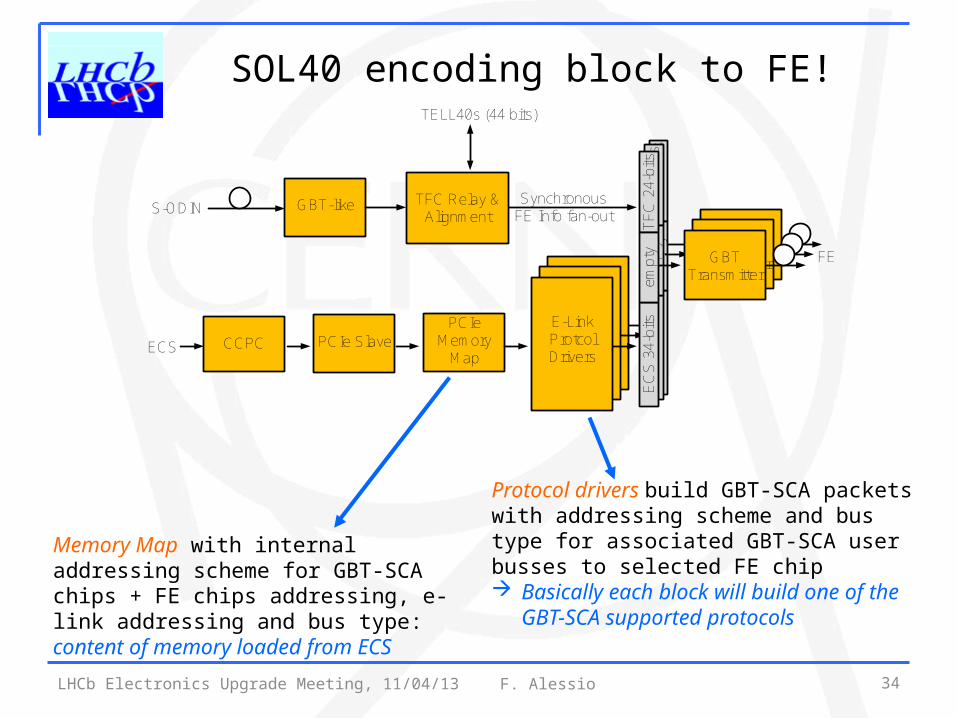
Protocol drivers build GBT-SCA packets with addressing scheme and bus type for associated GBT-SCA user busses to selected FE chip Basically each block will build one of
the GBT-SCA supported protocols
Memory Map with internal addressing scheme for GBT-SCA chips + FE chips addressing, e-link addressing and bus type: content of memory loaded from ECS
SOL40 encoding block to FE!
TF
C 2
4-bi
tsE
CS
34-
bits
empt
yT
FC
24-
bits
EC
S 3
4-bi
tsem
pty
E-LinkProtcolDrivers
GBT Transmitter
E-LinkProtcolDrivers
GBT Transmitter
PCIe SlavePCIe
MemoryMap
CCPC
TFC Relay & Alignment
GBT-like
TELL40s (44 bits)
S-ODINSynchronous
FE Info fan-out
ECS
FE
TF
C 2
4-bi
tsE
CS
34-
bitsE-Link
ProtcolDrivers
GBT Transmitterem
pty

LHCb Electronics Upgrade Meeting, 26/07/12 F. Alessio, R. Jacobsson
Usual considerations …
35
TFC+ECSInterface has the ECS load of an entire FE cluster for configurating and monitoring 34bits @ 40 MHz = 1.36Gb/s on single GBT link
• ~180 Gb/s for full TFC+ECSInterface (132 links)
• Single CCPC might become bottleneck… Clara & us, December 2011
How long to configure FE cluster? how many bits / FE? how many FEs/ GBT link? how many FEs / TFC+ECSInterface?
Numbers to be pinned down soon + GBT-SCA interfaces and protocols.
Readout CrateT
ELL
40
TE
LL40
TE
LL40
TE
LL40
TE
LL40
TE
LL40
TE
LL40
TE
LL40
FEs FEs FEsFEs...FEs FEs FEsFEs...FEs FEs FEsFEs...
SO
L40
ECS

LHCb Electronics Upgrade Meeting, 11/04/13 F. Alessio
Old TTC system support andrunning two systems in parallel
36
We already suggested the idea of a hybrid system:reminder: L0 electronics relying on TTC protocol part of the system runs with old TTC system part of the system runs with the new architecture
How?
1. Need connection between S-ODIN and ODIN (bidirectional) use dedicated RTM board on S-ODIN ATCA card
2. In an early commissioning phase ODIN is the master, S-ODIN is the slave S-ODIN task would be to distribute new commands to new FE, to new
TELL40s, and run processes in parallel to ODIN ODIN tasks are the ones today + S-ODIN controls the upgraded part
In this configuration, upgraded slice will run at 40 MHz, but positive triggers will come only at maximum 1.1MHz…
• Great testbench for development + tests + apprenticeship…• Bi-product: improve LHCb physics programme in 2015-2018…
3. In the final system, S-ODIN is the master, ODIN is the slave ODIN task is only to interface the L0 electronics path to S-ODIN
and toprovide clock resets on old TTC protocol

LHCb Electronics Upgrade Meeting, 11/04/13 F. Alessio
S-ODIN on Marseille’s ATCA board
37
S-ODIN
RJ45
CCPC GbE
FPGA
Clock crossbar
Serial crossbar
PCIe
Clock
Int. Comm.
MultiMaster
AMC
FARM
AMC
LLT Trigger
AMC
LHC Interfaces
AMC
FPGA
FPGA
FPGA
FPGA
Bac
kpla
ne c
onne
ctor
Clock
TFC+ Throttles
LHC Interfaces
LLT sub-trigger
FARM
TFC+ECS Interfaces
S-ODIN RTM
RT
M
conn
ecto
r
Ext
erna
l co
nnec
tors
à
OD
IN

LHCb Electronics Upgrade Meeting, 11/04/13 F. Alessio
TFC+ECSInterface on Marseille’s ATCA board
38
SOL40
RJ45
CCPC GbE
FPGA
Serial crossbar
PCIe
Clock
TFC + Throttles
FE
AMC
FE
AMC
FE
AMC
S-ODIN + FE
AMC
FPGA
FPGA
FPGA
MasterFPGA
Bac
kpla
ne c
onne
ctor
Clock
TFC+ Throttles
S-ODIN
FE (GBT, opt.)
FE (GBT)
FE (GBT)
FE (GBT)
Clock crossbar