Compiler Optimizations for Memory Hierarchy Chapter 20 trishulc/ tseng/ High Performance Compilers.
Storage Assignment and Memory
Optimizations during High-level
Synthesis for Configurable ArchitecturesWenrui Gong, Gang Wang, and Ryan Kastner
University of California, Santa Barbara.
Abstract
Modern, high performance configurable architectures integrate on-chip, distributed block
RAM modules to provide ample data storage. Synthesizing applications to these complex
systems requires an effective and efficient approach for data partitioning and storage as-
signment. In this paper, we formally describe this problem and show how it is much different
than the traditional data partitioning problem for compilation to parallel processing systems.
We present a data and iteration space partitioning solution that focuses on minimizing
remote memory accesses or, equivalently, maximizing the local computation. Using the same
code but different data partitionings, we can achieve up to 50% increase in frequency, without
increasing the number of cycles, by simply minimizing remote accesses. Other optimization
techniques like buffer insertion can further minimize remote accesses and lead to 46x
speedup in overall runtime.
Author’s address: Wenrui Gong, Gang Wang, and Ryan Kastner, University of California, Electrical and
Computer Engineering, Santa Barbara, 93106-9560 USA
May 1, 2006 DRAFT
1
Storage Assignment and Memory
Optimizations during High-level
Synthesis for Configurable Architectures
I. INTRODUCTION
Typical configurable computing systems consist of arrays of reconfigurable logic blocks
and flexible interconnect. In order to offer greater computing capabilities, high-performance
commercial configurable architectures provide ample configurable logic, and have integrated
a number of fixed components, including digital signal processing (DSP) and microprocessor
cores, custom hardware, and distributed block RAM modules. For instance, the Xilinx Virtex-
II Pro Platform FPGA series provides 3K to 125K logic cells, up to four PowerPC processor
cores and 1,738 kilobytes of distributed, embedded block RAM.
These configurable architectures, integrated with ample distributed block RAM modules,
exhibit superior computing abilities, storage capacities, and flexibilities over traditional
FPGAs. However, they currently lack the tools necessary to provide the application designer
efficient synthesis onto these complex architectures. In particular, there is a pressing need
for memory optimization techniques in the early stages of the design flow as modern con-
figurable architectures have a complex memory hierarchy, and earlier architectural-level
decisions greatly affect the final design qualities.
In traditional design flow of configurable devices, synthesis of block RAM modules are
generally handled as a physical problem. They are directly inferred from arrays, or in-
stantiated using vendor macros. They are packed a single component in placement, and
only partitioned when it is difficult to fit into the device. In most situations, the memory
bandwidth and storage capacities are not well utilized, and hence the generated designs are
not efficient in terms of latencies, throughput, and achieved frequencies.
This paper focuses on seeking a partitioning-based solution to the storage assignment
problem at the earliest stages of the design flow. We also show how other memory optimiza-
tions can achieve design goals, such as increase throughputs and reduce latencies, i.e. reduce
the number of clock cycles and increase the achievable clock frequencies.
May 1, 2006 DRAFT

2
The central contribution of this paper is a novel integrated approach of deriving an ap-
propriate data partitioning, and synthesizing the program behavior to configurable devices.
Through intensive research on the interplay between the data partitions and architectural
synthesis decisions, such as scheduling and binding, we show that designs that minimize
the number of global memory accesses and exhibit local computation can meet the design
goals, and minimize the execution time (or maximize the system throughput) under resource
constraints. Other optimization techniques, including buffer insertion, are applied to im-
prove maximum achieved clock frequencies and therefore improve the overall performance.
In particular, these optimizations further reduce latencies, and improve the achieve clock
frequencies.
This work is organized as follows. The next section gives details on the target configurable
architecture and the following section presents a motivating example. Section IV discusses
related work. Section V formally describes the data partitioning and storage assignment
problem and provides techniques to minimize the number of remote data memory accesses.
Section VI presents our experimental results and we conclude in Section VII.
II. TARGET CONFIGURABLE ARCHITECTURE
Many modern reconfigurable architectures incorporate a distributed memory module, amongst
their configurable logic blocks (CLBs). These architectures can be divided into homogeneous
and heterogeneous architectures according to the capacities and distribution of the RAM
blocks.
Mul
tiplie
r
Blo
ck R
AM
CLB
CLB
CLB
CLB
CLB
CLB
CLB
CLB
CLB
CLB
CLB
CLB
CLB
CLB
CLB
CLB
Mul
tiplie
r
Blo
ck R
AM
Mul
tiplie
r
Blo
ck R
AM
Mul
tiplie
r
Blo
ck R
AM
CLB
CLB
CLB
CLB
CLB
CLB
CLB
CLB
CLB
CLB
CLB
CLB
CLB
CLB
CLB
CLB
CLB
CLB
CLB
CLB
CLB
CLB
CLB
CLB
CLB
CLB
CLB
CLB
CLB
CLB
CLB
CLB
CLB
CLB
CLB
CLB
CLB
CLB
CLB
CLB
CLB
CLB
CLB
CLB
CLB
CLB
CLB
CLB
block RAM modules
Fig. 1. FPGA with distributed Block RAMs
Figure 1 presents an example of a homogeneous architecture. This roughly corresponds to
May 1, 2006 DRAFT
3
Xilinx Virtex II FPGA [1]. The block RAMs are evenly distributed on the chip and connected
with CLBs using reprogrammable interconnect. Every block RAM has the same capacity.
Additionally, there is an embedded multiplier located beside each block RAM. A large Virtex
II chip contains 168 blocks of 18 Kbits block RAM modules, providing 3,024 Kbits of on-chip
memory.
The heterogeneous architecture contains a variety of block RAM modules with different
capacities. For example, the TriMatrix memory on an Altera Stratix II FPGA chip [2] consists
of three types of on-chip block RAM modules: M512, M4K, and M-RAM. Their capacities are
576 bits, 4 Kbits, and 512 Kbits, respectively. A Stratix II chip may contain a large number
of M512 and M4K modules, but generally only a few M-RAM modules. Currently our work
only considers homogeneous architectures. However, if a design assigns a particular part of
such a device, which contains only one kind of RAM blocks. Under this circumstance, it is
possible to handle it as a homogeneous device.
ε
RA
M
RA
M
RA
M t t tt t tR
AM
RA
M
CL
B
6
�
?
����
Interconnect delayAccess latencyA fixed α
a variable
RA
M
Fig. 2. Total access latencies = α + ε
The access latency of the on-chip block RAM is equal to the propagation delay to the
memory port after the positive edge of the clock signal. This delay is usually a fixed number
α for a specific FPGA architecture. For example, α is 3.7 ns for Xilinx XC2V3000 FPGA.
Additionally it takes an extra ε ns to transfer data from the memory port to the accessing
CLB. Hence, a design running at 200MHz could take one clock cycle to retrieve data close
to the accessing CLB, but two or even more clock cycles to access data far away from the
CLB. On the other hand, it is often difficult to distinguish whether the data access is near
or far before placement and routing.
In addition to block RAM modules, CLBs can be configured as local memory, which is
convenient for storing intermediate results. When CLBs are configured as distributed mem-
ory, the access latency, i.e. the logic access time, is quite small. However, if a data array is
assigned to CLBs, an access involves extra delay for MUX selecting the addressed element.
May 1, 2006 DRAFT
4
For example, the delay for a 512 bit CLB memory is around 3.5 ns for Xilinx XC2V3000
FPGA; the delay for a 16 Kbit CLB memory increases to 6.2 ns.
The FPGA can be complimented by an external, global memory for storing large amounts
of data. Access latencies to the external memory depend on the bus protocol and type of
memory. The access latencies usually are an order of magnitude slower than those of on-
chip block RAM.
In this paper, we develop a methodology for partitioning data to distributed block RAM
modules. When compared to off-chip global memory and using CLBs as distributed RAM,
this approach is an effective and efficient solution for most applications.
III. MOTIVATING EXAMPLE: CORRELATION
In order to give the reader a understanding of the problem, we consider the synthesis of
a bank of correlators as a motivating example. This is a commonly occurring operation in
DSP applications, e.g. Kalman filters, matching pursuit (MP), recursive least squares (RLS),
and minimum mean-square error estimation (MMSE) [3].
The bank of correlators multiplies each sample of a received vector r with the correspond-
ing sample of a column in an S matrix, i.e. Ci =∑l
j=1 rj × Sj,i, where r is a vector of l
complex numbers, and S is a m× l real numbers. l and m will vary based on the application.
For instance, if we wish to perform radiolocation in the ISM band (i. e. 802.11x) using the
matching pursuit algorithm, both l and m are equal to 88 [4].
We assume a large enough memory module could be embedded in our chip, and assign the
S matrix on this memory module. The commercial high-level synthesis tool, such as Catapult
C, may generates a design with an extremely slow execution time of about 77,440 ns. Some
other tools may fail to synthesize this design due to the huge S matrix. On the other hand,
distributing the data accesses to block RAM modules results in designs that executes in up
to 80 times faster. Obviously the partitioning of the S matrix to the block RAM modules
greatly affects the system overall performance.
The data space is intuitively partitioned by column or by row. By simple analysis, column-
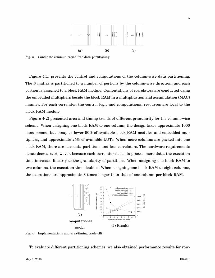
wise partition results in a communication-free partitioning. Figure 3 suggests several can-
didates column-wise partitionings. Figure 3(a), (b), and (c) assign one block RAM to one
column, four columns, and eight columns, respectively.
May 1, 2006 DRAFT
5
10 8685 87
(a)
84
8783
80
79
76
73
0 4
(b)
7
0 8
15 79
80
87
72
71
64
(c)
Fig. 3. Candidate communication-free data partitioning
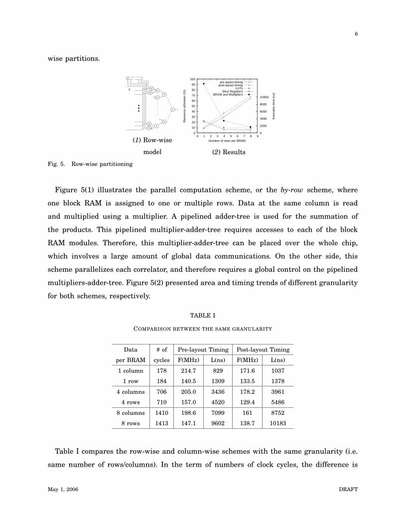
Figure 4(1) presents the control and computations of the column-wise data partitioning.
The S matrix is partitioned to a number of portions by the column-wise direction, and each
portion is assigned to a block RAM module. Computations of correlators are conducted using
the embedded multipliers beside the block RAM in a multiplication and accumulation (MAC)
manner. For each correlator, the control logic and computational resources are local to the
block RAM module.
Figure 4(2) presented area and timing trends of different granularity for the column-wise
scheme. When assigning one block RAM to one column, the design takes approximate 1000
nano second, but occupies lower 90% of available block RAM modules and embedded mul-
tipliers, and approximate 25% of available LUTs. When more columns are packed into one
block RAM, there are less data partitions and less correlators. The hardware requirements
hence decrease. However, because each correlator needs to process more data, the execution
time increases linearly to the granularity of partitions. When assigning one block RAM to
two columns, the execution time doubled. When assigning one block RAM to eight columns,
the executions are approximate 8 times longer than that of one column per block RAM.
rS
(1)
Computational
model
100
90
80
70
60
50
40
30
20
10
0 0 1 2 3 4 5 6 7 8 9
10000
8000
6000
4000
2000
0
Res
ourc
e ut
iliza
tion
(%)
Exe
cutio
n tim
e (n
s)
Number of columns per BRAM
pre-layout timingpost-layout timing
LUTsSlice Registers
BRAM and Multipliers
(2) Results
Fig. 4. Implementations and area/timing trade-offs
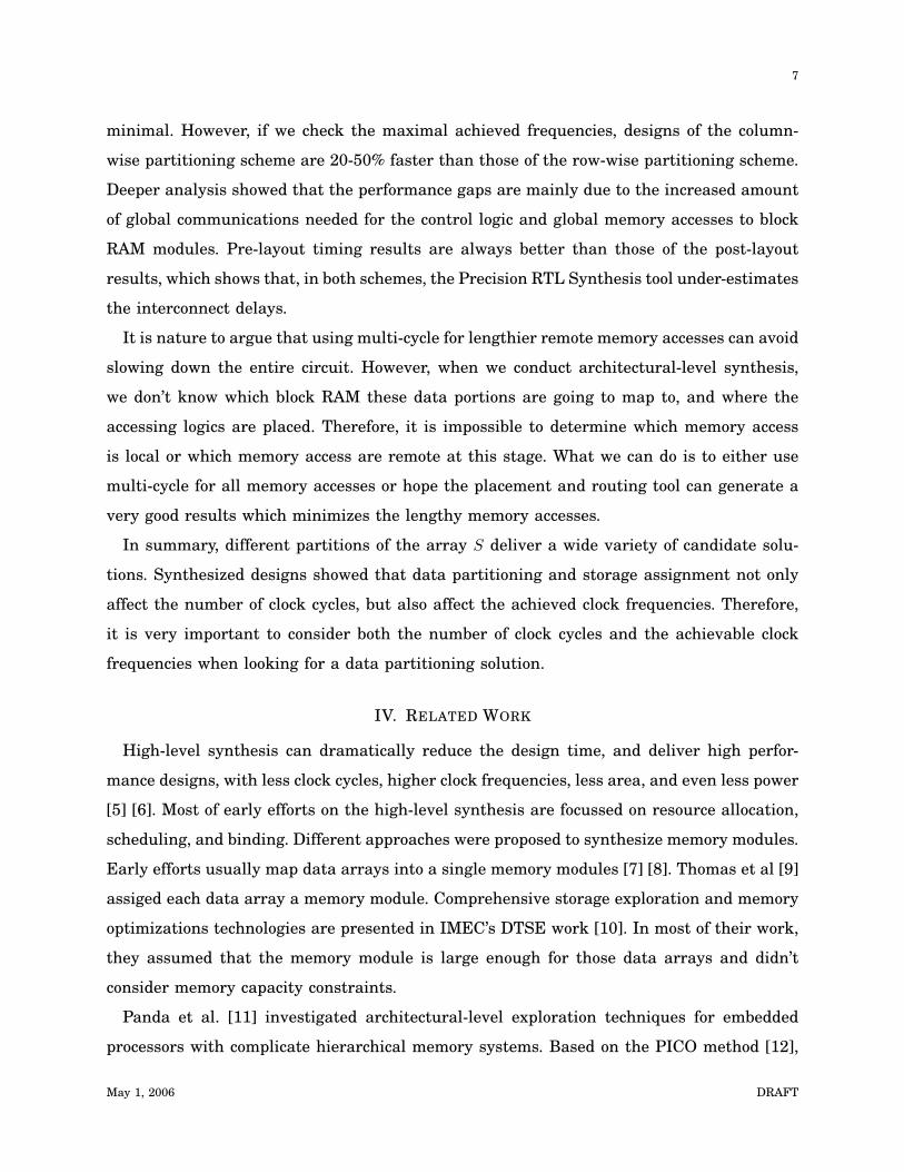
To evaluate different partitioning schemes, we also obtained performance results for row-
May 1, 2006 DRAFT
6
wise partitions.
r
S
(1) Row-wise
model
100
90
80
70
60
50
40
30
20
10
0 0 1 2 3 4 5 6 7 8 9
10000
8000
6000
4000
2000
0
Res
ourc
e ut
iliza
tion
(%)
Exe
cutio
n tim
e (n
s)
Number of rows per BRAM
pre-layout timingpost-layout timing
LUTsSlice Registers
BRAM and Multipliers
(2) Results
Fig. 5. Row-wise partitioning
Figure 5(1) illustrates the parallel computation scheme, or the by-row scheme, where
one block RAM is assigned to one or multiple rows. Data at the same column is read
and multiplied using a multiplier. A pipelined adder-tree is used for the summation of
the products. This pipelined multiplier-adder-tree requires accesses to each of the block
RAM modules. Therefore, this multiplier-adder-tree can be placed over the whole chip,
which involves a large amount of global data communications. On the other side, this
scheme parallelizes each correlator, and therefore requires a global control on the pipelined
multipliers-adder-tree. Figure 5(2) presented area and timing trends of different granularity
for both schemes, respectively.
TABLE I
COMPARISON BETWEEN THE SAME GRANULARITY
Data # of Pre-layout Timing Post-layout Timing
per BRAM cycles F(MHz) L(ns) F(MHz) L(ns)
1 column 178 214.7 829 171.6 1037
1 row 184 140.5 1309 133.5 1378
4 columns 706 205.0 3436 178.2 3961
4 rows 710 157.0 4520 129.4 5486
8 columns 1410 198.6 7099 161 8752
8 rows 1413 147.1 9602 138.7 10183
Table I compares the row-wise and column-wise schemes with the same granularity (i.e.
same number of rows/columns). In the term of numbers of clock cycles, the difference is
May 1, 2006 DRAFT
7
minimal. However, if we check the maximal achieved frequencies, designs of the column-
wise partitioning scheme are 20-50% faster than those of the row-wise partitioning scheme.
Deeper analysis showed that the performance gaps are mainly due to the increased amount
of global communications needed for the control logic and global memory accesses to block
RAM modules. Pre-layout timing results are always better than those of the post-layout
results, which shows that, in both schemes, the Precision RTL Synthesis tool under-estimates
the interconnect delays.
It is nature to argue that using multi-cycle for lengthier remote memory accesses can avoid
slowing down the entire circuit. However, when we conduct architectural-level synthesis,
we don’t know which block RAM these data portions are going to map to, and where the
accessing logics are placed. Therefore, it is impossible to determine which memory access
is local or which memory access are remote at this stage. What we can do is to either use
multi-cycle for all memory accesses or hope the placement and routing tool can generate a
very good results which minimizes the lengthy memory accesses.
In summary, different partitions of the array S deliver a wide variety of candidate solu-
tions. Synthesized designs showed that data partitioning and storage assignment not only
affect the number of clock cycles, but also affect the achieved clock frequencies. Therefore,
it is very important to consider both the number of clock cycles and the achievable clock
frequencies when looking for a data partitioning solution.
IV. RELATED WORK
High-level synthesis can dramatically reduce the design time, and deliver high perfor-
mance designs, with less clock cycles, higher clock frequencies, less area, and even less power
[5] [6]. Most of early efforts on the high-level synthesis are focussed on resource allocation,
scheduling, and binding. Different approaches were proposed to synthesize memory modules.
Early efforts usually map data arrays into a single memory modules [7] [8]. Thomas et al [9]
assiged each data array a memory module. Comprehensive storage exploration and memory
optimizations technologies are presented in IMEC’s DTSE work [10]. In most of their work,
they assumed that the memory module is large enough for those data arrays and didn’t
consider memory capacity constraints.
Panda et al. [11] investigated architectural-level exploration techniques for embedded
processors with complicate hierarchical memory systems. Based on the PICO method [12],
May 1, 2006 DRAFT
8
Kurdur et al. [13] presented an ILP formulation to solve the storage arrangement problem.
They assume every data array can fit into one of the local memory, and they use an extra
move operation to access remote data. These works are more like a processor-based data
exploration and memory optimization works.
Early efforts on utilizing multiple memory modules on FPGA [14] allocated an entire
array to a single memory module rather than partitioning data arrays. Furthermore, they
assumed that the latencies differences had little effect on system throughput. As to memory
optimization in synthesis to configurable platforms, Budiu et al. [15], and Diniz et al. [16],
respectively, presented some effective techniques to reduce memory accesses and benefit
high-level synthesis.
Huang et al. [17] presented their work in high-level synthesis with integrated data par-
titioning for ASIC design flow. Their work is quite similar to our work as they adapt code
analysis techniques from traditional parallelizing compilation field. However, their work was
more like in an ASIC flow and are not limited by the capacities of available memory modules.
They start from a fixed number of partitioning. Our proposed work starts from the program
cores and the resource constraints, and uses granularity adjustment to find out how many
partitions are reasonable for the design.
The data partitioning and storage assignment problem is well studied in the field of paral-
lelizing compilation [18] [19] [20]. Early efforts developed effective analysis techniques and
program transformations to reduce global communications and improve system performance.
Shih and Sheu [21] and Ramanujam and Sadayappan [22] addressed the methodology to
achieve communication-free iteration space and data partitioning problem. Pande [23] pre-
sented an communication-efficient data partitioning solution when it is impossible to get a
communication-free partitioning.
The following differences make it impossible to directly migrate these approaches into a
system compiler for configurable architectures with distributed block RAM modules.
• The target architectures are different. Multiprocessor systems have a fixed number of
microprocessors. Each microprocessor has its own local memory, and is connected with
a different remote memory modules that exhibit non uniform memory access (NUMA)
attributes.
• Configurable architectures execute programs using CLBs rather than microprocessors.
The number of block RAM modules are fixed. There is not fixed number of CLBs as-
May 1, 2006 DRAFT
9
sociated with a particular block RAM. Hence the boundaries between local and remote
memory are indistinct.
Our problem is distinguished from the previous studies as follows. First of all, these
differences violate a fundamental assumption held in the previous research. Most of the
previous efforts assumed that global communications or latencies to remote memory are an
order of magnitude slower than access latencies to local memory. This makes it reasonable
to simplify the objective function to simply reduce the amount of global communications.
This assumption is not true in the context of data partitioning for configurable archi-
tectures. As previously described, the boundaries between local and remote memory are
indistinct. Access latencies to block RAM modules depends on the distance between the
accessing CLBs and the memory ports. There is no way to determine the exact delay before
performing placement and routing.
Second, data partition and storage assignment have more compound effects on system per-
formance. In parallelizing compilation for multiprocessor architectures, once computations
and data are partitioned, it will be relatively easy to estimate the execution time since the
clock period is fixed, and the number of clock cycles consists of the communication overheads
and computation latencies for each instruction. However, it is extremely difficult to determine
the execution time in configurable systems before physical synthesis. Our results in Section
VI show that even though number of clock cycles are almost the same, there can be 30-50%
deviations in execution time due to variation in frequency. Therefore, the control logic and
computation times are effected, and not just the memory access delays.
Moreover, the flexibility to configure block RAM modules make this problem even more
difficult. Block RAM modules could be configured with a variety of width×depth schemes,
and as described before, even CLBs could be used to store small data arrays.
In summary, configurable architectures are drastically different from traditional NUMA
machines, making it difficult to estimate candidate solutions during the early stages of
synthesis. Flexibilities in configuring block RAM modules greatly enlarge the solution space,
making the problem even more challenging.
V. DATA PARTITIONING AND STORAGE ASSIGNMENT
This section formally describes the data partitioning and storage assignment problem, and
proposes an approach to computing the number of memory accesses for a given partition.
May 1, 2006 DRAFT

10
Then, we discuss some of the techniques that we use to reduce memory accesses and improve
system performance for FPGA-based configurable architectures with distributed block RAM
modules.
A. Problem formulation
We focus on data-intensive applications in digital signal processing. These applications
usually contain nested loops and multiple data arrays.
In order to simplify our problem, we assume that a) the input programs are nested loops;
b) index expressions of array references are affine functions of loop indices; c) there is no
indirect array references, or other similar pointer operations; d) all data arrays are assigned
to block RAM modules; and e) each data element is assigned one and only one single block
RAM modules, i.e. no duplicate data. Furthermore, we assume that all data types are fixed-
point numbers due to the current capability of our system compiler. If there are conditional
constructs, such as branch, transformation techniques, such as speculative execution and
loop normalization, could be applied to pre-process the input programs.
The inputs to this data partitioning and storage assignment problem are as follows:
• A program d contains an l-level perfectly nested loop L = {L1, L2, . . . , Ll}
• The program d accesses a set of n data arrays N = {N1, N2, . . . , Nn}.
• A specific target architecture, i.e. an FPGA, contains a set of m block RAM modules
M = {M1,M2, . . . ,Mm}. This FPGA also contains A CLBs.
• We set our desired frequency to F , and the maximum execution time to L.
The problem of data partitioning and storage assignment is to partition N into a set of p
data portions P = {P1, P2, . . . , Pp}, where p ≤ m, and seek an assignment {P →M} subject
to the following constraints
•⋃p
i=1 Pi = N, and Pi⋂
Pj = ∅, i.e. that all data arrays are assigned to block RAM and
each data element is assigned to one and only one block RAM module.
• ∀(Pi,Mj) ∈ {P→M}, the memory requirement of Pi is less than the capacity of Mj
After obtaining data partitions and storage assignment, we reconstruct the input program
d, and conduct behavioral-level synthesis. After RTL and physical synthesis, the synthesized
design must satisfy the following constraint:
• The slices of CLBs occupied by synthesized design d is less than A.
May 1, 2006 DRAFT

11
The objective is to minimize the total execution time (or maximize the system throughput)
under the resource constraints of specific configurable architectures. The desired frequency
F and the maximum execution time T are used as target metrics during compilation and
synthesis.
B. Overview of the proposed approach
Our proposed approach is based on our current efforts on synthesizing C programs into
RTL designs. Our system compiler takes C programs, performs necessary transformations
and optimizations. By specifying target architecture, and desired performance (throughput),
this compiler performs resource allocation, scheduling, and binding tasks, and generates
Verilog RTL designs, which can then be synthesized or simulated using commercial tools.
As discussed before, in configurable architectures, the boundaries between local and re-
mote accesses are indistinct. In our preliminary experiments, we found that, given the same
datapath with memory accesses to block RAM modules with different locations, the lengths
of critical path achieved after placement and routing can have a 30-50% variation. And a
limited number of functional units could be placed near the block RAM modules which they
access.
Therefore, we could still assume that, once the data space is partitioned, we can obtain
a corresponding partitioning of the iteration space, or a partitioning of the computations.
Each portion of the data space can be mapped to one portion of the iteration space. Then
we divide all memory accesses into local accesses and remote ones. However, these local and
remote memory accesses are different from those in parallel multiprocessor systems in that
the access latencies are usually on the same order of magnitude.
Based on this further assumption, we adapt some concepts and analysis techniques in
tradition parallelizing compilation. A Communication-free partitioning refers to a situation
when each partition of the iteration space only accesses the associated partition of the data
space. If we can not find a communication-free partitioning, we look for a communication-
efficient partitioning to minimize the execution time.
Our proposed approach integrates traditional program test and transformation techniques
in parallelizing compilation into our system compiler framework. In order to tackle the
performance estimation during data space partitioning, we use our behavioral-level synthesis
techniques, i.e. resource allocation, scheduling and binding.
May 1, 2006 DRAFT
12
C. Data and iteration space partitioning
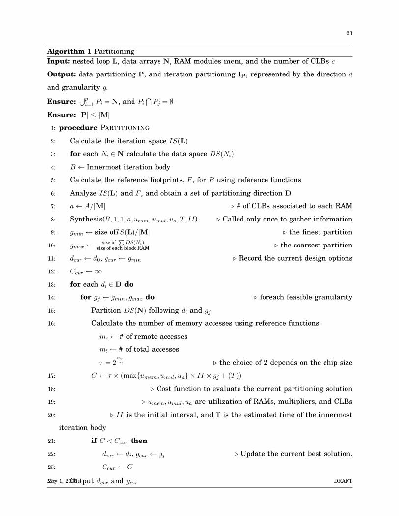
This section discusses our data and iteration space partitioning algorithm in detail. Our
approach is illustrated in Algorithm 1. Before line 7, we adapt existing analysis techniques
in parallelizing compilation to determine a set of directions to partition. In line 7 and 8, we
call our behavioral-synthesis algorithms to synthesize the innermost iteration body. After
that, we evaluate every candidate partitioning, and return the one with the most likelihood
achieving the short execution time subject to the resource constraints.
1) Program analysis: Given a l-level nested loops, the iteration space is an l-dimensional
integer space. The loop bounds of each nested level set the bounds of the iteration space. An
integer point in this iteration space solely refers to an iteration, which includes all state-
ments in the innermost iteration body. Each m-dimension data array has a corresponding
m-dimensional integer space. An integer point refers to a data element with that data index.
for (i=1; i<ROW-1; i++)
for (j=1; j<COL-1; j++)
d[i][j]=(s[i][j-1]+(s[i][j]<<1)+s[i][j+1])>>2;
Fig. 6. 1-dimensional mean filter
(2, 3)
j
i
(a) Iteration space
s[2][2−4]
col
row
(b) Data spaces of d and s
Fig. 7. Iteration space and data spaces of the 1D mean filter
For example, Figure 6 shows the kernel of a 1-dimensional mean filter. This simplest mean
filter blurs the image and removes speckles of high frequency noise in the row direction. The
corresponding iteration space is shown in Figure 7(a).
In each iteration, data elements in the data space are accessed. Since we assume that
index expressions of array references are affine functions of loop indices, a footprint of each
May 1, 2006 DRAFT
13
iteration can be calculated using the affine functions, i.e. each iteration is mapped to a set of
data points in the data space by means of specified array reference. In the above mean filter
example, given an iteration (2,3), we can easily obtain the access footprints in the DS((S))
as {(2, 2), (2, 3), (2, 4)} (as shown in the rectangle box in Figure 7(b)).
With the iteration space IS(L) and the reference footprints F , we can determine a set
of directions to partition the iteration space. The direction can be represented by a multi-
dimensional vector. For example, if we have a 2-level nested loop, we usually do row-wise or
column-wise partitioning, or in the (col, row) vector form, (0,1) or (1,0), respectively. Figure
8(a) shows a row-wise bi-partitioning of the iteration space of the above mean filter example,
and the corresponding data space partitioning is shown in Figure 8(b).
i
j
(a) Iteration space
rowcol
(b) Data spaces of d and s
Fig. 8. Data spaces are correspondingly partitioned when the iteration space is partitioned.
j
i
(a) Iteration space
row
col
(b) Data spaces of d and s
row
col
(c) Data spaces partition-
ing of d and s
Fig. 9. Partitioning of overlapped data access footprints
In the row-wise partitioning of the mean filter example, the data access footprints of any
iteration are in one of the data space portions. This could mean that, after synthesis and
May 1, 2006 DRAFT
14
physical design, all data accesses can be local memory accesses. However, in some cases,
data access footprints may be broken. Hence, some iterations may access data from more
than one data space partitions. As shown in Figure 9(b), the data in the rectangle boxes
are overlapped with the dashed box, i.e. data are required by iterations in both iteration
partitions This is the reason why we have non-local or remote data accesses. Although we
could not achieve communication-free partitioning, we could evenly partition the overlapped
data spaces. For instance, this arrays are partitioned like these boxes shown in Figure 9(c).
As to some applications, there may be other partitioning directions, such as a vector (1,1).
There could be a number of feasible partitioning solutions. However, it is possible to limit
our design spaces by seeking partitioning directions which result the least overlapped data
access footprints.
Above shows how we can partition the data and iteration space when the dimension of
iteration space equals to that of the data space. If the dimension of the data space is higher
than that of the iteration space, then a sub-space of the data space are accessed during
execution, and other parts of the data space do not affect the synthesized circuits. We can
apply similar approach to determine the data space partitioning. When the dimension of the
iteration space is higher than that of the data spaces, except some simple cases, it is very
hard to partition the data space and map those portions to block RAM modules.
2) Synthesis of iteration bodies: In order to evaluate our candidate solutions, their perfor-
mance on target configurable architectures should be determined. Since most design prob-
lems in behavior synthesis are NP -complete, and time-consuming, it is extremely inefficient
to perform synthesis on each candidate solutions.
In our approach, we first synthesize the innermost iteration body with proper resource
constraint, obtain performance results for the single iteration, and then use them to evaluate
our cost function in line 17 of Algorithm 1.
The innermost iteration body is scheduled and pipelined using allocated resources, includ-
ing 1 block RAM modules, 1 embedded multipliers, and a portion of CLBs, which, by our
assumption, are associated with a specific block RAM module. The design is pipelined using
allocated resources. The execution time and achieved throughput are reported. For a large
iteration space IS(L), the pipelined iteration body gives the shortest execution time, or the
highest throughput, and the best resource utilization. After synthesis, we return the resource
utilization for the block RAM, multiplier, and the CLBs, respectively. We also output the
May 1, 2006 DRAFT
15
number of total clock cycles, and the initial interval (II), which determines the maximum
system throughput. In case that there are true data dependencies between iterations, no
additional transformations are applied to solve these dependencies since our goal is to gather
performance information, mainly the resource utilization, which .
3) Granularity adjustment: For each partitioning direction, we evaluate every possible
partition granularity. Given a specific nested loop and data arrays, and a specific archi-
tecture, we can determine the finest and coarsest grain for a homogeneous partitioning. As
shown in line 9 of Algorithm 1, the finest partition granularity partitions the iteration space
(and the data space) into as many portions as possible. It hence depends on the number of
block RAM modules. The coarsest grained partition requires that each block RAM store as
much data as possible. It depends on the capacity of a block RAM module.
Our cost function, C ← τ×(max{umem, umul, ua}×II×gj+(T )), as shown in line 17, give us a
good idea how long the execution time will be. It consists of two parts. The first one is the τ , a
ratio factor of the global memory accesses over all memory accesses, which is greater than or
equal to 1, as shown in line 16. This τ includes effects of remote memory accesses. When there
is no remote memory access, τ = 1, and we can achieve a communication-free partitioning;
otherwise, we want to minimize it, which reduces the execution time. The second part is an
experiential formula estimating the total clock cycles for a pipelined design under resource
constraints. Since the iteration body is pipelined, the most utilized components determines
the performance (or throughput) when more than one iterations are assigned to this block.
For example, after pipelining, II = 1, T = 10, max{umem, umul, uc} = umul = 1. All multipliers
are busy at all time. If there are ten iterations in one partition, then the execution time will
be 1 × II × 10 + (T − II) = 19 clock cycles, without considering effects of remote memory
accesses. Another example could be, after pipelining, II = 1, T = 10, max{umem, umul, uc} =
umul = 0.5, there are still ten iterations in one partition, then the execution time will be
0.5 × II × 10 + (T − II) = 14 clock cycles, without considering effects of remote memory
accesses. The reason why the second one is faster is that the half of multipliers and more
of other resources are free, which allow more operations are scheduled and executed at the
same time.
May 1, 2006 DRAFT
16
D. Improving Clock Frequencies
The maximum achieved clock frequency greatly affects the overall performance of the
generated design. However, it is very difficult to accurately estimate the clock frequency
before placement and routing.
The motivating example show up to 25% differences between the pre-layout and post-
layout timing results. When the granularities of the data partitions decrease, the differences
between the pre-layout and the post-layout timing results increases since that, the finer the
partition granularity is, the more partitions there are and the more complicated designs are
generated.
(a)
(d)
Blo
ck R
AM
CLB
CLB
CLB
CLB
CLB
CLB
CLB
CLB
CLB
CLB
CLB
CLB
CLB
CLB
CLB
CLBM
ultip
lier
Blo
ck R
AM
CLB
CLB
CLB
CLB
CLB
CLB
(a) (b)(c)+
Mul
tiplie
r
=⇒
(b)
register
Blo
ck R
AM
CLB
CLB
CLB
CLB
CLB
CLB
CLB
CLB
CLB
CLB
CLB
CLB
CLB
CLB
Mul
tiplie
r
Blo
ck R
AM
CLB
CLB
CLB
CLB
CLB
CLB
CLB
(a) (b)(c)+ CLB(d)
Mul
tiplie
r
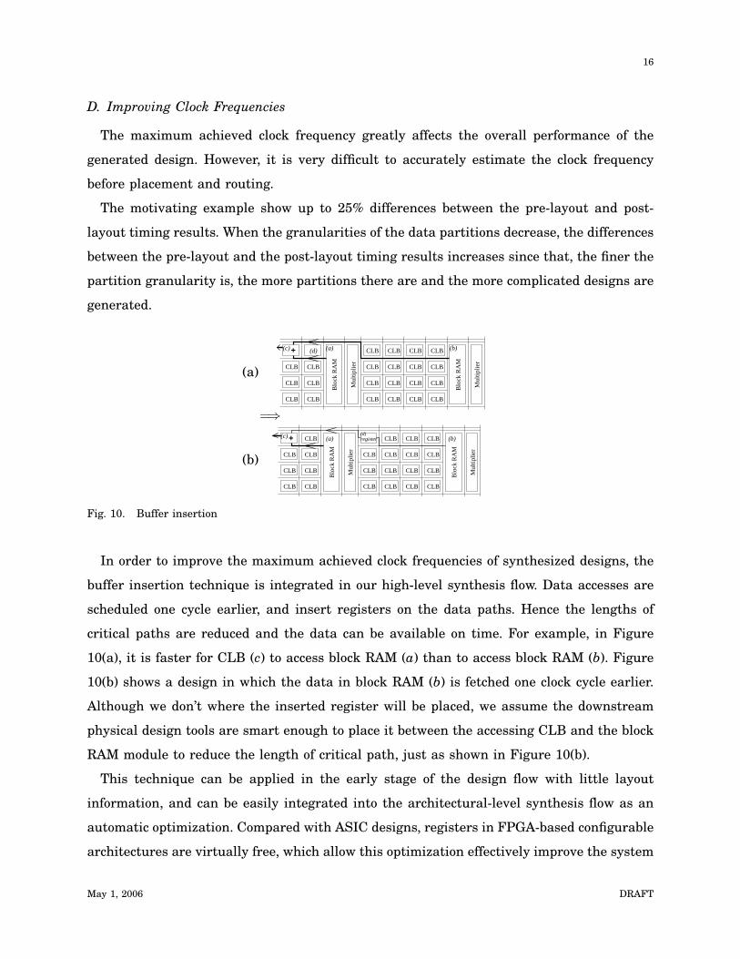
Fig. 10. Buffer insertion
In order to improve the maximum achieved clock frequencies of synthesized designs, the
buffer insertion technique is integrated in our high-level synthesis flow. Data accesses are
scheduled one cycle earlier, and insert registers on the data paths. Hence the lengths of
critical paths are reduced and the data can be available on time. For example, in Figure
10(a), it is faster for CLB (c) to access block RAM (a) than to access block RAM (b). Figure
10(b) shows a design in which the data in block RAM (b) is fetched one clock cycle earlier.
Although we don’t where the inserted register will be placed, we assume the downstream
physical design tools are smart enough to place it between the accessing CLB and the block
RAM module to reduce the length of critical path, just as shown in Figure 10(b).
This technique can be applied in the early stage of the design flow with little layout
information, and can be easily integrated into the architectural-level synthesis flow as an
automatic optimization. Compared with ASIC designs, registers in FPGA-based configurable
architectures are virtually free, which allow this optimization effectively improve the system
May 1, 2006 DRAFT

17
performance with little cost.
VI. EXPERIMENTAL RESULTS
This section presents our experimental setup and results.
A. Experimental Setup
Our benchmark suite consist of several DSP and image processing applications. SOBEL
edge detection, which applies horizontal and vertical detection masks to an input image.
Bilinear filtering is a suitable way to eliminate blocky textures in 3-D image engine.
2D Gauss applies lowpass filtering to 2D arrays aka blurring 2D images, and 1D Gauss
is more general lowpass filter. A number of DSP and image applications have the similar
control structure and memory access patterns, such as texture smoothing and convolution
[24]. Except the SOBEL ones, all other four algorithm cores have the same input size and
resource constraints.
The target architecture is Xilinx Virtex II FPGA series, which contains evenly distributed
block RAM modules. The target frequency was set to 150 MHz for our benchmark suite.
This frequency represents a typical clock frequencies of high-speed designs for the specific
target Virtex II FPGA. There is no other special reason for us to select this particular clock
frequency.
We partitioned the arrays using the algorithm proposed in Section 4.2, and performed
program transformations, and generate RTL hardware designs. We then used Precision RTL
Synthesis and Xilinx physical design tools to obtain area and timing results. Experiments
results are collected after RTL synthesis and placement and routing.
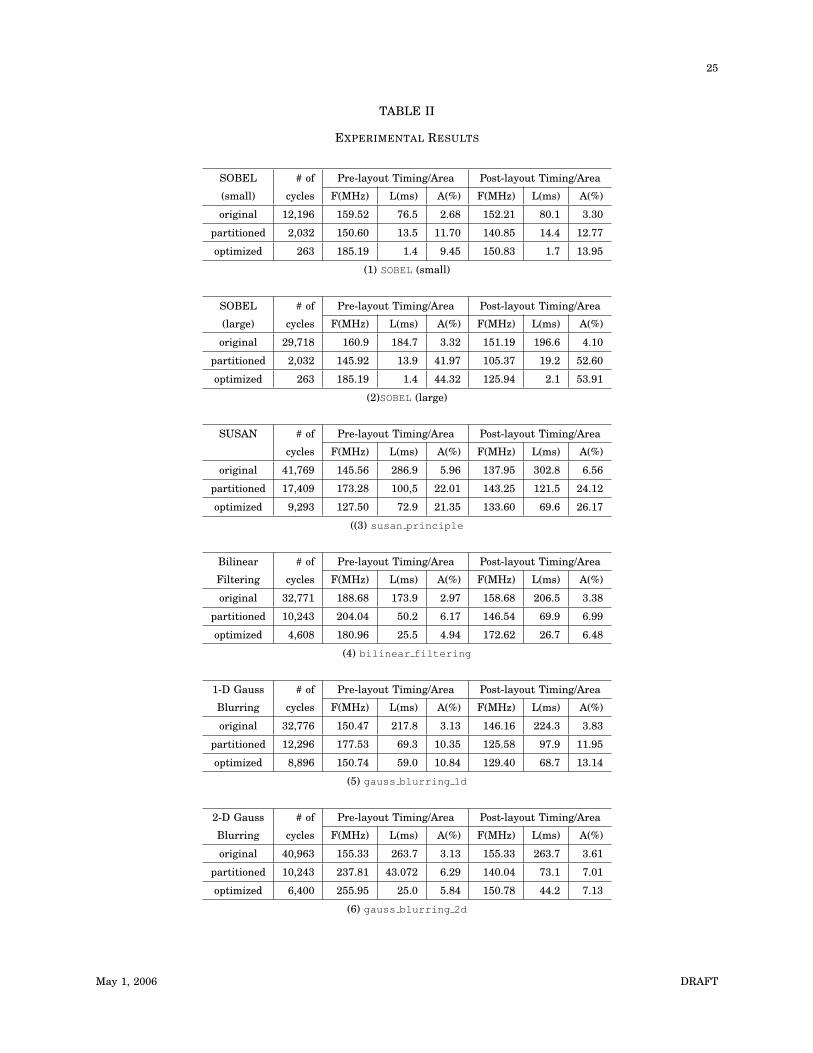
Table II presents detailed results of these benchmarks. For each benchmark, there is
an original design, of where the iteration space and data spaces are not partitioned, a
partitioned design, of which the iteration space and data spaces are partitioned under the
resource constraints, and an optimized design, on which more memory optimizations, scalar
replacement and buffer insertions, are applied. There are timing and area results for both
pre-layout and post-layout designs. For each design, the number of clock cycles are reported.
With the reported clock frequencies, we can calculated the execution time before actual
physical synthesis. After placement and routing, the achieved clock frequencies are collected,
and the execution time are calculated.
May 1, 2006 DRAFT
18
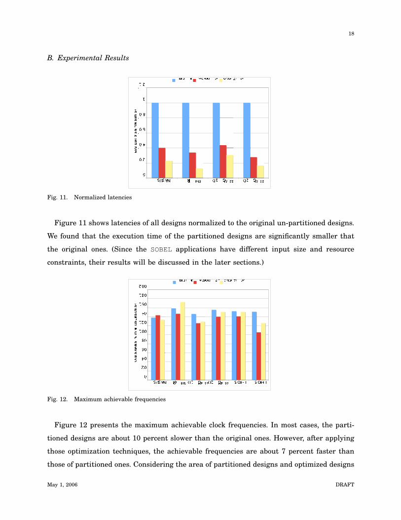
B. Experimental Results
00. 20. 40. 60. 8
11 . 2
S U S A N B i l in e a r 1D G au s s 2 D G au s s
N orm alizi edL aten ci es
O r ig i n a l P a r t i t io n e d Op t im iz e d
Fig. 11. Normalized latencies
Figure 11 shows latencies of all designs normalized to the original un-partitioned designs.
We found that the execution time of the partitioned designs are significantly smaller that
the original ones. (Since the SOBEL applications have different input size and resource
constraints, their results will be discussed in the later sections.)
02 04 06 08 01 0 01 2 01 4 01 6 01 8 02 0 0
S U S A N B i l in e a r 1D G au s s 2 D G au s s S O B E L S O B E LA chi ev abl e Cl ockFr e quen ci es
O r ig in a l P a r t i t io n e d Op t im iz e d
Fig. 12. Maximum achievable frequencies
Figure 12 presents the maximum achievable clock frequencies. In most cases, the parti-
tioned designs are about 10 percent slower than the original ones. However, after applying
those optimization techniques, the achievable frequencies are about 7 percent faster than
those of partitioned ones. Considering the area of partitioned designs and optimized designs
May 1, 2006 DRAFT
19
are much larger than the original ones and with more complicated control, these results are
quite good.
If we only partition the data arrays, the number of clock cycles is reduced, and the maximal
frequencies after placement and routing are slower than our desired frequencies. In order
to reduce memory accesses, optimization techniques such as buffer insertion and scalar
replacement are utilized.
After partitioning, the average speedup over the original ones is 2.75 times faster, and
after further optimizations, the average speedup is 4.80 times faster.
The buffer insertion is an effective optimization to improve the achieved clock frequencies.
Comparing optimized designs with partitioned designs, clock frequencies after placement
and routing are improved 8% in average, and up to 20% percent. Among half of those designs,
the optimized designs could finally achieve the 150 MHz goals design target. These improve-
ments on achieved clock frequencies are considered more important than the decreases of
the numbers of clock cycles since that the improvements on clock frequencies can speed up
the execution of the whole design, if other modules can run at higher clock frequencies.
C. Performance effects of partitioning decisions
Tables II(1) and II(2) show timing results for SOBEL edge detection with two different
input image sizes. In the smaller design, we achieve the 150 MHz design goal, and with a
46x speedup compared to the original design. However, we could not achieve the design goal
in the larger SOBEL design. The constraints on the block RAM modules results the original
design partitioned into up to 16 portions, which is hard for later stages of placement and
routing. This points to the fact that as the number of partitions increases, the effects of
physical designs on performance also increases, hence the clock frequencies decrease.
D. Summary
Architectural-level decision on data partition and storage assignment in the early stage
could affect the final result greatly. In general, a partitioned design will decrease execution
time, but occupies more memory and hardware resources. Different optimization techniques
can be utilized to reduce memory access, and improve the overall performance. When the
size of designs increase, it becomes more difficult to achieve design goals since it lacks the
support from down-stream tools, especially physical design tools.
May 1, 2006 DRAFT
20
VII. CONCLUSION
Modern configurable computing systems offer enormous computing capacities, and con-
tinue to integrate on-chip computation and storage components. Advanced synthesis tools
are required to map large applications to these increasingly complicated chips. More impor-
tantly, these tools must be powerful and smart enough to conduct memory optimizations to
effectively utilize on-chip distributed block RAM modules.
This work showed that a data and iteration space partitioning approach integrated with
existing architectural-level synthesis techniques can parallelize input designs, and dramat-
ically improve system performance. Experimental results indicated that partitioned designs
achieve much better performance.
In future work, we plan to investigate analysis and transformation techniques to deal
with configurable architectures with heterogeneous memory arrangment. It will also be
interesting to have better buffer insertion techniques for different design complexities.
ACKNOWLEDGMENT
The authors would like to thank...
May 1, 2006 DRAFT
21
REFERENCES
[1] Virtex-II Platform FPGAs: Complete Data Sheet, Xilinx, Inc., October 2003.
[2] Stratix II Device Handbook, Altera Corporation, January 2005.
[3] S. Haykin, Adaptive Filter Theory, Fourth Edition. Englewood Cliffs, NJ: Prentice Hall, 2001.
[4] Y. Meng, A. P. Brown, R. A. Iltis, T. S. herwood, H. Lee, and R. Kastner, “Mp core: Algorithm and design
techniques for efficient channel estimation in wireless applications,” in Proceedings of the 42nd Design
Automation Conference (DAC), Anaheim, California, USA, June 2005.
[5] G. De Micheli, Synthesis and Optimization of Digital Circuits. Hightstown, NJ: McGraw-Hill, Inc., 1994.
[6] D. D. Gajski and L. Ramachandran, “Introduction to High-Level synthesis,” IEEE Design and Test of
Computers, vol. 11, no. 4, pp. 44–54, Winter 1994.
[7] R. J. Cloutier and D. E. Thomas, “The Combination of Scheduling, Allocation, and Mapping in a Single
Algorithm,” in Proceedings of the 27th ACM/IEEE Design Automation Conference, 1990.
[8] H. De Man, F. Catthoor, G. Goossens, J. Vanhoof, J. V. Meerbergen, S. Note, and J. Huisken, “Architecture-
driven synthesis techniques for VLSl implementation of DSP algorithms,” Proc. of the IEEE, vol. 78, no. 2,
pp. 319–35, February 1990.
[9] D. E. Thomas, E. D. Lagnese, J. A. Nestor, J. V. Rajan, R. L. Blackburn, and R. A. Walker, Algorithmic
and Register-Transfer Level Synthesis: The System Architect’s Workbench. Norwell, MA: Kluwer Academic
Publishers, 1989.
[10] F. Catthoor, K. Danckart, C. Kulkarni, E. Brockmeyer, P. G. Kjeldsberg, T. Van Achteren, and T. Omnes,
Data Access and Storage Management for Embedded Programmable Processors. Norwell, MA: Kluwer
Academic Publishers, 2002.
[11] P. R. Panda, N. D. Dutt, and A. Nicolau, “Exploiting Off-Chip Memory Access Modes in High-Level
Synthesis,” in Proceedings of the 1997 IEEE/ACM International Conference on Computer-Aided Design,
1997.
[12] R. Schreiber, S. Aditya, S. Mahlke, V. Kathail, B. R. Rau, D. Cronquist, and M. Sivaraman, “Pico-npa: High-
level synthesis of nonprogrammable hardware accelerators,” Journal of VLSI Signal Processing Systems,
vol. 31, no. 2, pp. 127–42, June 2002.
[13] M. Kudlur, K. Fan, M. Chu, and S. Mahlke, “Automatic synthesis of customized local memories for
multicluster application accelerators,” in Proceedings of IEEE 15th International Conference on Application-
Specific Systems, Architectures and Processors, 2004.
[14] M. B. Gokhale and J. M. Stone, “Automatic Allocation of Arrays to Memories in FPGA Processors with
Multiple Memory Banks,” in Proceedings of the Seventh Annual IEEE Symposium on Field-Programmable
Custom Computing Machines, 1999.
[15] M. Budiu and S. C. Goldstein, “Optimizing Memory Accesses For Spatial Computation,” in International
Symposium on Code Generation and Optimization, 2003.
[16] N. Baradaran and P. C. Diniz, “A register allocation algorithm in the presence of scalar replacement for fine-
grain configurable architectures,” in Proceedings of the 2005 Conferenc on Design Automation and Testing
in Europe (DATE05), 2005.
[17] C. Huang, S. Ravi, A. Raghunathan, and N. K. Jha, “High-Level Synthesis of Distributed Logic-Memory
May 1, 2006 DRAFT
22
Architectures,” in Proceedings of the 2002 IEEE/ACM International Conference on Computer-Aided Design.
San Jose, California: ACM Press, 2002.
[18] R. Allen and K. Kennedy, Optimizing Compilers for Modern Architectures. San Francisco, CA: Morgan
Karfmann Publishers, 2002.
[19] S. Pande and D. P. Agrawal, Eds., Compiler Optimizations for Scalable Parallel Systems: Languages,
Compilation Techniques, and Run Time Systems. Heidelberg, Germany: Springer, 2001.
[20] M. Wolfe, High Performance Compilers for Parallel Computing. Redwood City, CA: Addison-Wesley, 1996.
[21] K.-P. Shih, J.-P. Sheu, and C.-H. Huang, “Statement-Level Communication-Free Partitioning Techniques
for Parallelizing Compilers,” in Proceedings of the 9th Workshop on Languages and Compilers for Parallel
Computing, 1996.
[22] J. Ramanujam and P. Sadayappan, “Compile-time Techniques for Data Distribution in Distributed Memory
Machines,” IEEE Transactions on Parallel and Distributed Systems, vol. 2, no. 4, pp. 472–82, October 1991.
[23] S. Pande, “A Compile Time Partitioning Method for DOALL Loops on Distributed Memory Systems,” in
Proceedings of 1996 International Conference on Parallel Processing, 1996.
[24] R. C. Gonzalez and R. E. Woods, Digital Image Processing, 2nd Edition. Englewood Cliffs, NJ: Prentice
Hall, 2002.
May 1, 2006 DRAFT
23
Algorithm 1 PartitioningInput: nested loop L, data arrays N, RAM modules mem, and the number of CLBs c
Output: data partitioning P, and iteration partitioning IP, represented by the direction d
and granularity g.
Ensure:⋃p
i=1 Pi = N, and Pi⋂
Pj = ∅
Ensure: |P| ≤ |M|
1: procedure PARTITIONING
2: Calculate the iteration space IS(L)
3: for each Ni ∈ N calculate the data space DS(Ni)
4: B ← Innermost iteration body
5: Calculate the reference footprints, F , for B using reference functions
6: Analyze IS(L) and F , and obtain a set of partitioning direction D
7: a← A/|M| . # of CLBs associated to each RAM
8: Synthesis(B, 1, 1, a, uram, umul, ua, T, II) . Called only once to gather information
9: gmin ← size ofIS(L)/|M| . the finest partition
10: gmax ← size ofP
DS(Ni)size of each block RAM . the coarsest partition
11: dcur ← d0, gcur ← gmin . Record the current design options
12: Ccur ←∞
13: for each di ∈ D do
14: for gj ← gmin, gmax do . foreach feasible granularity
15: Partition DS(N) following di and gj
16: Calculate the number of memory accesses using reference functions
mr ← # of remote accesses
mt ← # of total accesses
τ = 2mrmt . the choice of 2 depends on the chip size
17: C ← τ × (max{umem, umul, ua} × II × gj + (T ))
18: . Cost function to evaluate the current partitioning solution
19: . umem, umul, ua are utilization of RAMs, multipliers, and CLBs
20: . II is the initial interval, and T is the estimated time of the innermost
iteration body
21: if C < Ccur then
22: dcur ← di, gcur ← gj . Update the current best solution.
23: Ccur ← C
24: Output dcur and gcurMay 1, 2006 DRAFT
24
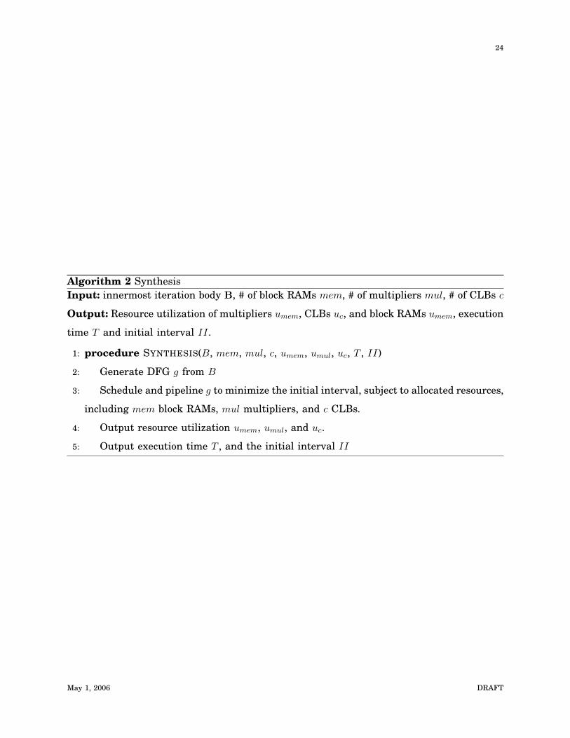
Algorithm 2 SynthesisInput: innermost iteration body B, # of block RAMs mem, # of multipliers mul, # of CLBs c
Output: Resource utilization of multipliers umem, CLBs uc, and block RAMs umem, execution
time T and initial interval II.
1: procedure SYNTHESIS(B, mem, mul, c, umem, umul, uc, T , II)
2: Generate DFG g from B
3: Schedule and pipeline g to minimize the initial interval, subject to allocated resources,
including mem block RAMs, mul multipliers, and c CLBs.
4: Output resource utilization umem, umul, and uc.
5: Output execution time T , and the initial interval II
May 1, 2006 DRAFT
25
TABLE II
EXPERIMENTAL RESULTS
SOBEL # of Pre-layout Timing/Area Post-layout Timing/Area
(small) cycles F(MHz) L(ms) A(%) F(MHz) L(ms) A(%)
original 12,196 159.52 76.5 2.68 152.21 80.1 3.30
partitioned 2,032 150.60 13.5 11.70 140.85 14.4 12.77
optimized 263 185.19 1.4 9.45 150.83 1.7 13.95
(1) SOBEL (small)
SOBEL # of Pre-layout Timing/Area Post-layout Timing/Area
(large) cycles F(MHz) L(ms) A(%) F(MHz) L(ms) A(%)
original 29,718 160.9 184.7 3.32 151.19 196.6 4.10
partitioned 2,032 145.92 13.9 41.97 105.37 19.2 52.60
optimized 263 185.19 1.4 44.32 125.94 2.1 53.91
(2)SOBEL (large)
SUSAN # of Pre-layout Timing/Area Post-layout Timing/Area
cycles F(MHz) L(ms) A(%) F(MHz) L(ms) A(%)
original 41,769 145.56 286.9 5.96 137.95 302.8 6.56
partitioned 17,409 173.28 100,5 22.01 143.25 121.5 24.12
optimized 9,293 127.50 72.9 21.35 133.60 69.6 26.17
((3) susan principle
Bilinear # of Pre-layout Timing/Area Post-layout Timing/Area
Filtering cycles F(MHz) L(ms) A(%) F(MHz) L(ms) A(%)
original 32,771 188.68 173.9 2.97 158.68 206.5 3.38
partitioned 10,243 204.04 50.2 6.17 146.54 69.9 6.99
optimized 4,608 180.96 25.5 4.94 172.62 26.7 6.48
(4) bilinear filtering
1-D Gauss # of Pre-layout Timing/Area Post-layout Timing/Area
Blurring cycles F(MHz) L(ms) A(%) F(MHz) L(ms) A(%)
original 32,776 150.47 217.8 3.13 146.16 224.3 3.83
partitioned 12,296 177.53 69.3 10.35 125.58 97.9 11.95
optimized 8,896 150.74 59.0 10.84 129.40 68.7 13.14
(5) gauss blurring 1d
2-D Gauss # of Pre-layout Timing/Area Post-layout Timing/Area
Blurring cycles F(MHz) L(ms) A(%) F(MHz) L(ms) A(%)
original 40,963 155.33 263.7 3.13 155.33 263.7 3.61
partitioned 10,243 237.81 43.072 6.29 140.04 73.1 7.01
optimized 6,400 255.95 25.0 5.84 150.78 44.2 7.13
(6) gauss blurring 2d
May 1, 2006 DRAFT