CS252 Graduate Computer Architecture Lecture 16 Cache Optimizations (Con’t) Memory Technology
62
CS252 Graduate Computer Architecture Lecture 16 Cache Optimizations (Con’t) Memory Technology John Kubiatowicz Electrical Engineering and Computer Sciences University of California, Berkeley http://www.eecs.berkeley.edu/~kubitron/ cs252 http://www-inst.eecs.berkeley.edu/~cs252
description
CS252 Graduate Computer Architecture Lecture 16 Cache Optimizations (Con’t) Memory Technology. John Kubiatowicz Electrical Engineering and Computer Sciences University of California, Berkeley http://www.eecs.berkeley.edu/~kubitron/cs252 http://www-inst.eecs.berkeley.edu/~cs252. - PowerPoint PPT Presentation
Transcript of CS252 Graduate Computer Architecture Lecture 16 Cache Optimizations (Con’t) Memory Technology

CS252Graduate Computer Architecture
Lecture 16
Cache Optimizations (Con’t)Memory Technology
John KubiatowiczElectrical Engineering and Computer Sciences
University of California, Berkeley
http://www.eecs.berkeley.edu/~kubitron/cs252http://www-inst.eecs.berkeley.edu/~cs252

3/19/2007 cs252-S07, Lecture 16 2
Review: Cache performance
CycleTimeyMissPenaltMissRateInst
MemAccessCPIICCPUtime Execution
• Miss-oriented Approach to Memory Access:
• Separating out Memory component entirely– AMAT = Average Memory Access Time
CycleTimeAMATInst
MemAccessCPIICCPUtime AluOps
yMissPenaltMissRateHitTimeAMAT DataDataData
InstInstInst
yMissPenaltMissRateHitTimeyMissPenaltMissRateHitTime

3/19/2007 cs252-S07, Lecture 16 3
Review: 6 Basic Cache Optimizations• Reducing hit time1. Avoiding Address Translation during Cache
Indexing• E.g., Overlap TLB and cache access, Virtual Addressed Caches
• Reducing Miss Penalty2. Giving Reads Priority over Writes
• E.g., Read complete before earlier writes in write buffer3. Multilevel Caches
• Reducing Miss Rate4. Larger Block size (Compulsory misses)5. Larger Cache size (Capacity misses)6. Higher Associativity (Conflict misses)

3/19/2007 cs252-S07, Lecture 16 4
1. Fast hits by Avoiding Address Translation
• Send virtual address to cache? Called Virtually Addressed Cache or just Virtual Cache vs. Physical Cache
– Every time process is switched logically must flush the cache; otherwise get false hits
» Cost is time to flush + “compulsory” misses from empty cache– Dealing with aliases (sometimes called synonyms);
Two different virtual addresses map to same physical address– I/O must interact with cache, so need virtual address
• Solution to aliases– HW guaranteess covers index field & direct mapped, they must be unique;
called page coloring
• Solution to cache flush– Add process identifier tag that identifies process as well as address within
process: can’t get a hit if wrong process

3/19/2007 cs252-S07, Lecture 16 5
Two options for avoiding translation:CPU
TB
$
MEM
VA
PA
PA
Physically Addressed(“indexed)
ConventionalOrganization
CPU
$
TB
MEM
VA
VA
PA
Virtually Addressed (“indexed”)Cache Translate only on miss
Synonym Problem
VATags
CPU
$ TB
MEM
VA
PATags
PA
Still Physically IndexedOverlap $ access
with VA translation:requires $ index to
remain invariantacross translation
L2 $
Variation A Variation B

3/19/2007 cs252-S07, Lecture 16 6
3. Multi-level cache
• L2 EquationsAMAT = Hit TimeL1 + Miss RateL1 x Miss PenaltyL1
Miss PenaltyL1 = Hit TimeL2 + Miss RateL2 x Miss PenaltyL2
AMAT = Hit TimeL1 + Miss RateL1 x (Hit TimeL2 + Miss RateL2 + Miss PenaltyL2)
• Definitions:– Local miss rate— misses in this cache divided by the total number of
memory accesses to this cache (Miss rateL2)– Global miss rate—misses in this cache divided by the total number of
memory accesses generated by the CPU (Miss RateL1 x Miss RateL2)
– Global Miss Rate is what matters

3/19/2007 cs252-S07, Lecture 16 7
Review: (Con’t)12 Advanced Cache Optimizations• Reducing hit time1.Small and simple
caches2.Way prediction3.Trace caches
• Increasing cache bandwidth
4.Pipelined caches5.Multibanked caches6.Nonblocking caches
• Reducing Miss Penalty7. Critical word first8. Merging write buffers
• Reducing Miss Rate9. Victim Cache10. Hardware prefetching11. Compiler prefetching12. Compiler
Optimizations

3/19/2007 cs252-S07, Lecture 16 8
4: Increasing Cache Bandwidth by Pipelining
• Pipeline cache access to maintain bandwidth, but higher latency
• Instruction cache access pipeline stages:1: Pentium2: Pentium Pro through Pentium III 4: Pentium 4
greater penalty on mispredicted branches more clock cycles between the issue of the load
and the use of the data

3/19/2007 cs252-S07, Lecture 16 9
5. Increasing Cache Bandwidth: Non-Blocking Caches
• Non-blocking cache or lockup-free cache allow data cache to continue to supply cache hits during a miss
– requires F/E bits on registers or out-of-order execution– requires multi-bank memories
• “hit under miss” reduces the effective miss penalty by working during miss vs. ignoring CPU requests
• “hit under multiple miss” or “miss under miss” may further lower the effective miss penalty by overlapping multiple misses
– Significantly increases the complexity of the cache controller as there can be multiple outstanding memory accesses
– Requires muliple memory banks (otherwise cannot support)– Penium Pro allows 4 outstanding memory misses

3/19/2007 cs252-S07, Lecture 16 10
Value of Hit Under Miss for SPEC (old data)
• FP programs on average: AMAT= 0.68 -> 0.52 -> 0.34 -> 0.26• Int programs on average: AMAT= 0.24 -> 0.20 -> 0.19 -> 0.19• 8 KB Data Cache, Direct Mapped, 32B block, 16 cycle miss, SPEC 92
Hit Under i Misses
Avg.
Mem
. Acc
ess
Tim
e
0
0.2
0.4
0.6
0.8
1
1.2
1.4
1.6
1.8
2
eqnt
ott
espr
esso
xlisp
com
pres
s
mdl
jsp2 ear
fppp
pto
mca
tv
swm
256
dodu
csu
2cor
wave
5
mdl
jdp2
hydr
o2d
alvi
nn
nasa
7sp
ice2g
6or
a
0->1
1->2
2->64
Base
Integer Floating Point
“Hit under n Misses”
0->11->22->64Base
3/19/2007 cs252-S07, Lecture 16 11
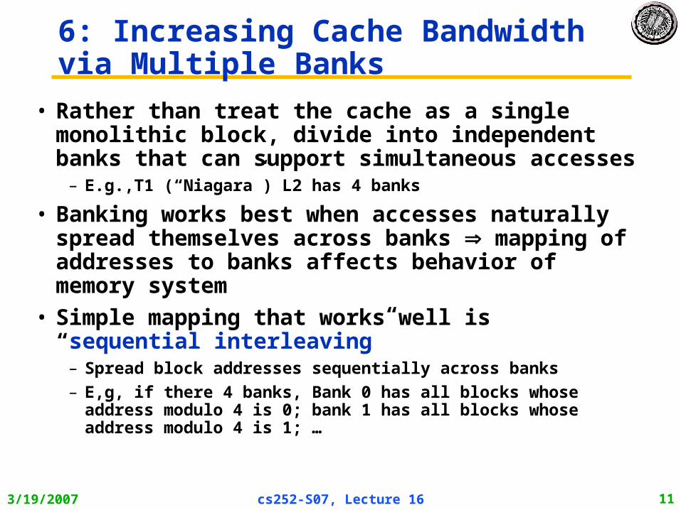
6: Increasing Cache Bandwidth via Multiple Banks
• Rather than treat the cache as a single monolithic block, divide into independent banks that can support simultaneous accesses
– E.g.,T1 (“Niagara”) L2 has 4 banks
• Banking works best when accesses naturally spread themselves across banks mapping of addresses to banks affects behavior of memory system
• Simple mapping that works well is “sequential interleaving”
– Spread block addresses sequentially across banks– E,g, if there 4 banks, Bank 0 has all blocks whose address modulo 4
is 0; bank 1 has all blocks whose address modulo 4 is 1; …

3/19/2007 cs252-S07, Lecture 16 12
7. Reduce Miss Penalty: Early Restart and Critical Word First
• Don’t wait for full block before restarting CPU• Early restart—As soon as the requested word of the
block arrives, send it to the CPU and let the CPU continue execution
– Spatial locality tend to want next sequential word, so not clear size of benefit of just early restart
• Critical Word First—Request the missed word first from memory and send it to the CPU as soon as it arrives; let the CPU continue execution while filling the rest of the words in the block
– Long blocks more popular today Critical Word 1st Widely used
block

3/19/2007 cs252-S07, Lecture 16 13
8. Merging Write Buffer to Reduce Miss Penalty• Write buffer to allow processor to continue
while waiting to write to memory• If buffer contains modified blocks, the
addresses can be checked to see if address of new data matches the address of a valid write buffer entry
• If so, new data are combined with that entry• Increases block size of write for write-through
cache of writes to sequential words, bytes since multiword writes more efficient to memory
• The Sun T1 (Niagara) processor, among many others, uses write merging

3/19/2007 cs252-S07, Lecture 16 14
9. Reducing Misses: a “Victim Cache”
• How to combine fast hit time of direct mapped yet still avoid conflict misses?
• Add buffer to place data discarded from cache
• Jouppi [1990]: 4-entry victim cache removed 20% to 95% of conflicts for a 4 KB direct mapped data cache
• Used in Alpha, HP machinesTo Next Lower Level In
Hierarchy
DATATAGS
One Cache line of DataTag and Comparator
One Cache line of DataTag and Comparator
One Cache line of DataTag and Comparator
One Cache line of DataTag and Comparator

3/19/2007 cs252-S07, Lecture 16 15
10. Reducing Misses by Hardware Prefetching of Instructions & Data
• Prefetching relies on having extra memory bandwidth that can be used without penalty
• Instruction Prefetching– Typically, CPU fetches 2 blocks on a miss: the requested block and the next
consecutive block. – Requested block is placed in instruction cache when it returns, and prefetched
block is placed into instruction stream buffer• Data Prefetching
– Pentium 4 can prefetch data into L2 cache from up to 8 streams from 8 different 4 KB pages
– Prefetching invoked if 2 successive L2 cache misses to a page, if distance between those cache blocks is < 256 bytes
1.16
1.45
1.18 1.20 1.21 1.26 1.29 1.32 1.40 1.49
1.97
1.001.201.401.601.802.002.20
Per
form
ance
Impr
ovem
ent
SPECint2000 SPECfp2000

3/19/2007 cs252-S07, Lecture 16 16
11. Reducing Misses by Software Prefetching Data
• Data Prefetch– Load data into register (HP PA-RISC loads)– Cache Prefetch: load into cache
(MIPS IV, PowerPC, SPARC v. 9)– Special prefetching instructions cannot cause faults;
a form of speculative execution
• Issuing Prefetch Instructions takes time– Is cost of prefetch issues < savings in reduced misses?– Higher superscalar reduces difficulty of issue bandwidth

3/19/2007 cs252-S07, Lecture 16 17
12. Reducing Misses by Compiler Optimizations
• McFarling [1989] reduced caches misses by 75% on 8KB direct mapped cache, 4 byte blocks in software
• Instructions– Reorder procedures in memory so as to reduce conflict misses– Profiling to look at conflicts(using tools they developed)
• Data– Merging Arrays: improve spatial locality by single array of compound elements
vs. 2 arrays– Loop Interchange: change nesting of loops to access data in order stored in
memory– Loop Fusion: Combine 2 independent loops that have same looping and some
variables overlap– Blocking: Improve temporal locality by accessing “blocks” of data repeatedly vs.
going down whole columns or rows

3/19/2007 cs252-S07, Lecture 16 18
Merging Arrays Example/* Before: 2 sequential arrays */int val[SIZE];int key[SIZE];
/* After: 1 array of stuctures */struct merge {
int val;int key;
};struct merge merged_array[SIZE];
Reducing conflicts between val & key; improve spatial locality

3/19/2007 cs252-S07, Lecture 16 19
Loop Interchange Example/* Before */for (k = 0; k < 100; k = k+1)
for (j = 0; j < 100; j = j+1)for (i = 0; i < 5000; i = i+1)x[i][j] = 2 * x[i][j];
/* After */for (k = 0; k < 100; k = k+1)
for (i = 0; i < 5000; i = i+1)for (j = 0; j < 100; j = j+1)x[i][j] = 2 * x[i][j];
Sequential accesses instead of striding through memory every 100 words; improved spatial locality
3/19/2007 cs252-S07, Lecture 16 20
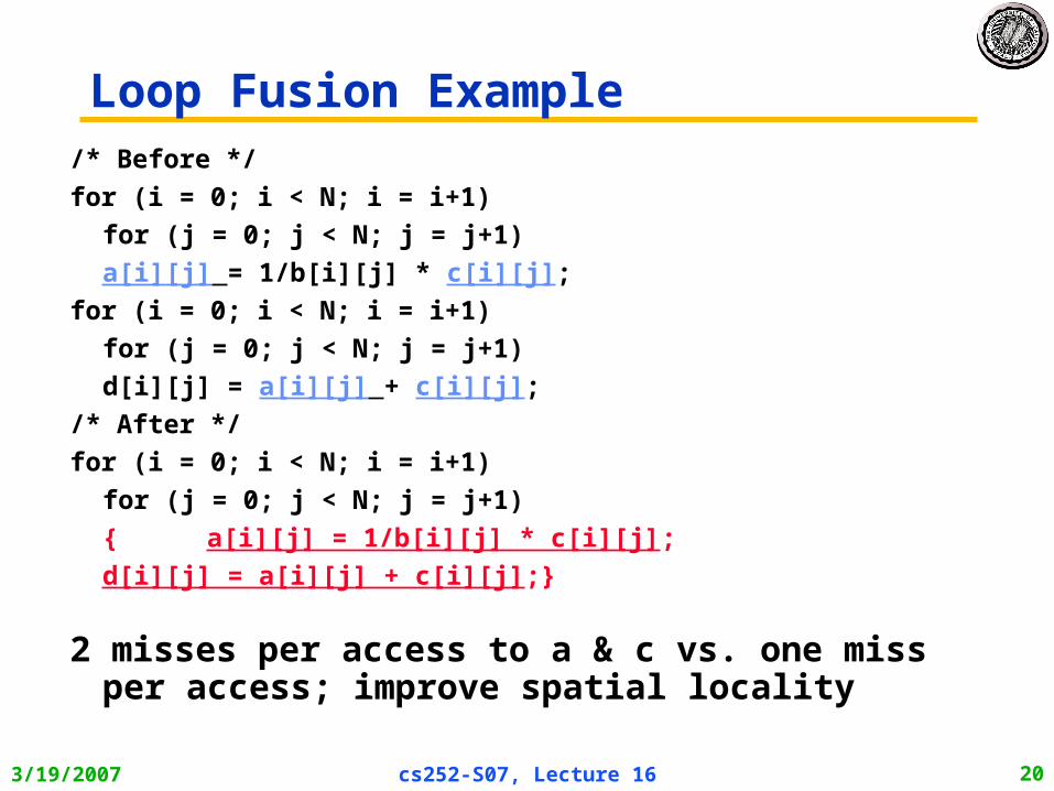
Loop Fusion Example/* Before */for (i = 0; i < N; i = i+1)
for (j = 0; j < N; j = j+1)a[i][j] = 1/b[i][j] * c[i][j];
for (i = 0; i < N; i = i+1)for (j = 0; j < N; j = j+1)d[i][j] = a[i][j] + c[i][j];
/* After */for (i = 0; i < N; i = i+1)
for (j = 0; j < N; j = j+1){ a[i][j] = 1/b[i][j] * c[i][j];d[i][j] = a[i][j] + c[i][j];}
2 misses per access to a & c vs. one miss per access; improve spatial locality

3/19/2007 cs252-S07, Lecture 16 21
Blocking Example/* Before */for (i = 0; i < N; i = i+1)
for (j = 0; j < N; j = j+1){r = 0; for (k = 0; k < N; k = k+1){r = r + y[i][k]*z[k][j];}; x[i][j] = r;};
• Two Inner Loops:– Read all NxN elements of z[]– Read N elements of 1 row of y[] repeatedly– Write N elements of 1 row of x[]
• Capacity Misses a function of N & Cache Size:– 2N3 + N2 => (assuming no conflict; otherwise …)
• Idea: compute on BxB submatrix that fits

3/19/2007 cs252-S07, Lecture 16 22
Blocking Example
/* After */for (jj = 0; jj < N; jj = jj+B)for (kk = 0; kk < N; kk = kk+B)for (i = 0; i < N; i = i+1)
for (j = jj; j < min(jj+B-1,N); j = j+1){r = 0; for (k = kk; k < min(kk+B-1,N); k = k+1) {r = r + y[i][k]*z[k][j];}; x[i][j] = x[i][j] + r;};
• B called Blocking Factor• Capacity Misses from 2N3 + N2 to 2N3/B +N2
• Conflict Misses Too?

3/19/2007 cs252-S07, Lecture 16 23
Reducing Conflict Misses by Blocking
• Conflict misses in caches not FA vs. Blocking size– Lam et al [1991] a blocking factor of 24 had a fifth the misses vs. 48
despite both fit in cache
Blocking Factor
Mis
s Ra
te
0
0.05
0.1
0 50 100 150
Fully Associative Cache
Direct Mapped Cache

3/19/2007 cs252-S07, Lecture 16 24
Performance Improvement 1 1.5 2 2.5 3
compress
cholesky(nasa7)
spicemxm (nasa7)btrix (nasa7)
tomcatvgmty (nasa7)
vpenta (nasa7)
mergedarrays
loopinterchange
loop fusion blocking
Summary of Compiler Optimizations to Reduce Cache Misses (by hand)

3/19/2007 cs252-S07, Lecture 16 25
Compiler Optimization vs. Memory Hierarchy Search
• Compiler tries to figure out memory hierarchy optimizations
• New approach: “Auto-tuners” 1st run variations of program on computer to find best combinations of optimizations (blocking, padding, …) and algorithms, then produce C code to be compiled for that computer
• “Auto-tuner” targeted to numerical method– E.g., PHiPAC (BLAS), Atlas (BLAS),
Sparsity (Sparse linear algebra), Spiral (DSP), FFT-W

3/19/2007 cs252-S07, Lecture 16 26
Reference
Best: 4x2
Mflop/s
Mflop/s
Sparse Matrix – Search for Blockingfor finite element problem [Im, Yelick, Vuduc, 2005]

3/19/2007 cs252-S07, Lecture 16 27
Best Sparse Blocking for 8 Computers
• All possible column block sizes selected for 8 computers; How could compiler know?
Intel Pentium M
Sun Ultra 2, Sun Ultra 3,
AMD Opteron
IBM Power 4, Intel/HP Itanium
Intel/HP Itanium 2
IBM Power 3
8
4
2
1
1 2 4 8
row
blo
ck s
ize
(r)
column block size (c)
3/19/2007 cs252-S07, Lecture 16 28
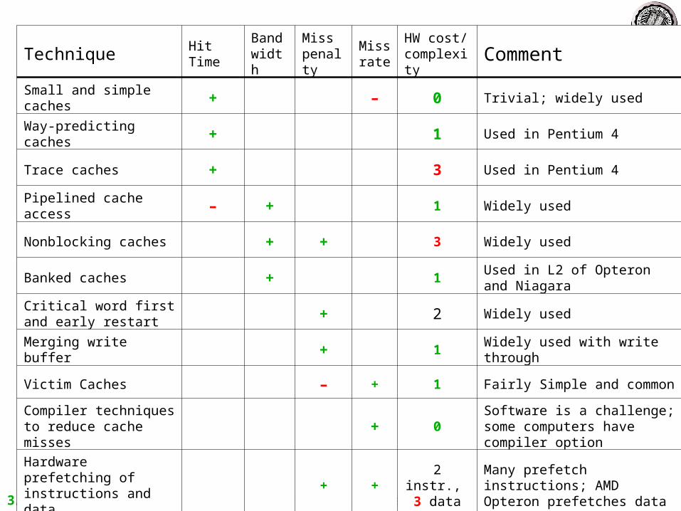
Technique Hit Time
Bandwidth
Miss penalty
Miss rate
HW cost/ complexity Comment
Small and simple caches + – 0 Trivial; widely used
Way-predicting caches + 1 Used in Pentium 4
Trace caches + 3 Used in Pentium 4
Pipelined cache access – + 1 Widely used
Nonblocking caches + + 3 Widely used
Banked caches + 1 Used in L2 of Opteron and Niagara
Critical word first and early restart + 2 Widely used
Merging write buffer + 1 Widely used with write through
Victim Caches – + 1 Fairly Simple and common
Compiler techniques to reduce cache misses + 0 Software is a challenge; some
computers have compiler option
Hardware prefetching of instructions and data + + 2 instr.,
3 dataMany prefetch instructions; AMD Opteron prefetches data
Compiler-controlled prefetching + + 3 Needs nonblocking cache; in
many CPUs

3/19/2007 cs252-S07, Lecture 16 29
AMD Opteron Memory Hierarchy• 12-stage integer pipeline yields a maximum clock rate of 2.8
GHz and fastest memory PC3200 DDR SDRAM• 48-bit virtual and 40-bit physical addresses• I and D cache: 64 KB, 2-way set associative, 64-B block, LRU• L2 cache: 1 MB, 16-way, 64-B block, pseudo LRU• Data and L2 caches use write back, write allocate • L1 caches are virtually indexed and physically tagged• L1 I TLB and L1 D TLB: fully associative, 40 entries
– 32 entries for 4 KB pages and 8 for 2 MB or 4 MB pages • L2 I TLB and L1 D TLB: 4-way, 512 entities of 4 KB pages• Memory controller allows up to 10 cache misses
– 8 from D cache and 2 from I cache

3/19/2007 cs252-S07, Lecture 16 30
Opteron Memory Hierarchy Performance
• For SPEC2000– I cache misses per instruction is 0.01% to 0.09% – D cache misses per instruction are 1.34% to 1.43% – L2 cache misses per instruction are 0.23% to 0.36%
• Commercial benchmark (“TPC-C-like”)– I cache misses per instruction is 1.83% (100X!)– D cache misses per instruction are 1.39% ( same)– L2 cache misses per instruction are 0.62% (2X to 3X)
• How compare to ideal CPI of 0.33?

3/19/2007 cs252-S07, Lecture 16 31
CPI breakdown for Integer Programs
-0.501.001.502.002.503.00
perlb
mk
craf
ty
eon
gzip
gap
vorte
x
bzip
2
gcc
pars
er vpr
twol
f
TPC
-C
CPI
Min Pipeline StallMax Memory CPIBase CPI
• CPI above base attributable to memory 50%• L2 cache misses 25% overall (50% memory CPI)
– Assumes misses are not overlapped with the execution pipeline or with each other, so the pipeline stall portion is a lower bound
3/19/2007 cs252-S07, Lecture 16 32
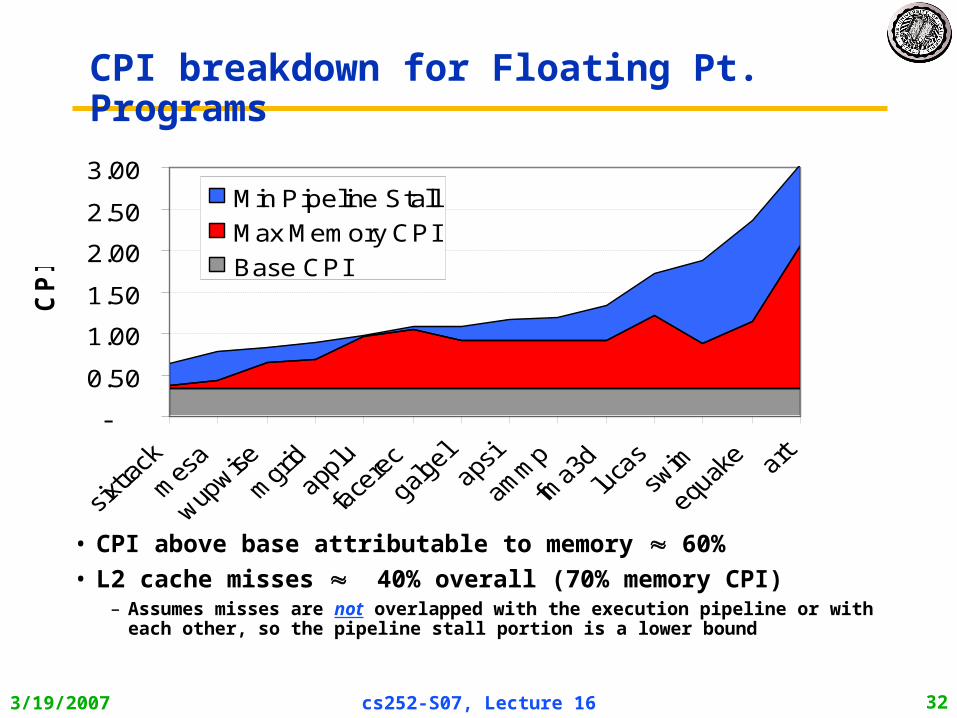
CPI breakdown for Floating Pt. Programs
• CPI above base attributable to memory 60%• L2 cache misses 40% overall (70% memory CPI)
– Assumes misses are not overlapped with the execution pipeline or with each other, so the pipeline stall portion is a lower bound
-
0.50
1.00
1.50
2.00
2.50
3.00
CPI
Min Pipeline StallMax Memory CPIBase CPI
3/19/2007 cs252-S07, Lecture 16 33
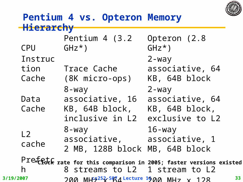
Pentium 4 vs. Opteron Memory Hierarchy
CPU Pentium 4 (3.2 GHz*) Opteron (2.8 GHz*)Instruction Cache
Trace Cache (8K micro-ops)
2-way associative, 64 KB, 64B block
Data Cache
8-way associative, 16 KB, 64B block, inclusive in L2
2-way associative, 64 KB, 64B block, exclusive to L2
L2 cache 8-way associative, 2 MB, 128B block
16-way associative, 1 MB, 64B block
Prefetch 8 streams to L2 1 stream to L2
Memory 200 MHz x 64 bits 200 MHz x 128 bits*Clock rate for this comparison in 2005; faster versions existed

3/19/2007 cs252-S07, Lecture 16 34
Misses Per Instruction: Pentium 4 vs. Opteron
-
1
2
3
4
5
6
7gz
ip vpr
gcc
mcf
cra f
ty
wup
wis
e
swim
mgr
id
appl
u
mes
a
Rat
io o
f MP
I: P
entiu
m 4
/Opt
eron
D cache: P4/Opteron
L2 cache: P4/Opteron
SPECint2000 SPECfp2000
Opteron better
Pentium better
• D cache miss: P4 is 2.3X to 3.4X vs. Opteron• L2 cache miss: P4 is 0.5X to 1.5X vs. Opteron• Note: Same ISA, but not same instruction count
2.3X3.4X
0.5X
1.5X

3/19/2007 cs252-S07, Lecture 16 35
Fallacies and Pitfalls• Not delivering high memory bandwidth in a cache-based system
– 10 Fastest computers at Stream benchmark [McCalpin 2005]– Only 4/10 computers rely on data caches, and their memory BW
per processor is 7X to 25X slower than NEC SX7
1,000
10,000
100,000
1,000,000
System Memory BW
Per Processor Memory BW

3/19/2007 cs252-S07, Lecture 16 36
Main Memory Background• Performance of Main Memory:
– Latency: Cache Miss Penalty» Access Time: time between request and word arrives» Cycle Time: time between requests
– Bandwidth: I/O & Large Block Miss Penalty (L2)
• Main Memory is DRAM: Dynamic Random Access Memory– Dynamic since needs to be refreshed periodically (8 ms, 1% time)– Addresses divided into 2 halves (Memory as a 2D matrix):
» RAS or Row Address Strobe» CAS or Column Address Strobe
• Cache uses SRAM: Static Random Access Memory– No refresh (6 transistors/bit vs. 1 transistor
Size: DRAM/SRAM 4-8, Cost/Cycle time: SRAM/DRAM 8-16

3/19/2007 cs252-S07, Lecture 16 37
Main Memory Deep Background• “Out-of-Core”, “In-Core,” “Core Dump”?• “Core memory”?• Non-volatile, magnetic• Lost to 4 Kbit DRAM (today using 512Mbit DRAM)• Access time 750 ns, cycle time 1500-3000 ns

3/19/2007 cs252-S07, Lecture 16 38
Core Memories (1950s & 60s)
• Core Memory stored data as magnetization in iron rings
– Iron “cores” woven into a 2-dimensional mesh of wires– Origin of the term “Dump Core”– Rumor that IBM consulted Life Saver company
• See: http://www.columbia.edu/acis/history/core.html
The first magnetic core memory, from the IBM 405 Alphabetical Accounting Machine.

3/19/2007 cs252-S07, Lecture 16 39
DRAM logical organization (4 Mbit)
• Square root of bits per RAS/CAS
Column Decoder
Sense Amps & I/O
Memory Array(2,048 x 2,048)
A0…A10
…11 D
Q
Word Line Storage Cell

3/19/2007 cs252-S07, Lecture 16 40
Quest for DRAM Performance1. Fast Page mode
– Add timing signals that allow repeated accesses to row buffer without another row access time
– Such a buffer comes naturally, as each array will buffer 1024 to 2048 bits for each access
2. Synchronous DRAM (SDRAM)– Add a clock signal to DRAM interface, so that the repeated
transfers would not bear overhead to synchronize with DRAM controller
3. Double Data Rate (DDR SDRAM)– Transfer data on both the rising edge and falling edge of the
DRAM clock signal doubling the peak data rate– DDR2 lowers power by dropping the voltage from 2.5 to 1.8
volts + offers higher clock rates: up to 400 MHz– DDR3 drops to 1.5 volts + higher clock rates: up to 800 MHz
• Improved Bandwidth, not Latency

3/19/2007 cs252-S07, Lecture 16 41
DRAM name based on Peak Chip Transfers / SecDIMM name based on Peak DIMM MBytes / Sec
Stan-dard
Clock Rate (MHz)
M transfers / second
DRAM Name
Mbytes/s/ DIMM
DIMM Name
DDR 133 266 DDR266 2128 PC2100
DDR 150 300 DDR300 2400 PC2400
DDR 200 400 DDR400 3200 PC3200
DDR2 266 533 DDR2-533 4264 PC4300
DDR2 333 667 DDR2-667 5336 PC5300
DDR2 400 800 DDR2-800 6400 PC6400
DDR3 533 1066 DDR3-1066 8528 PC8500
DDR3 666 1333 DDR3-1333 10664 PC10700
DDR3 800 1600 DDR3-1600 12800 PC12800x 2 x 8
Fast
est f
or s
ale
4/06
($12
5/G
B)
3/19/2007 cs252-S07, Lecture 16 42
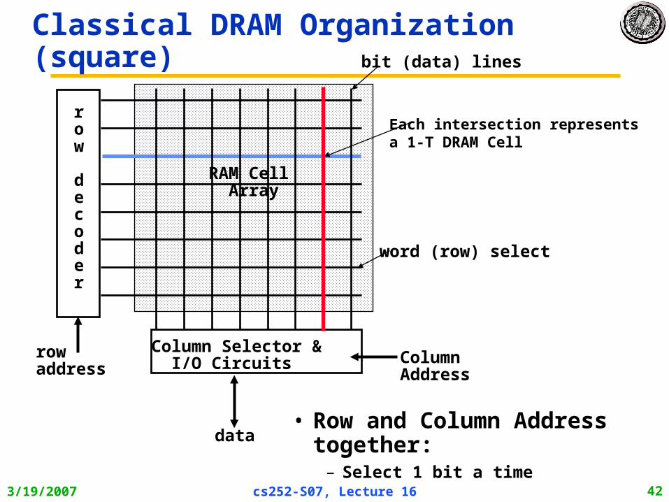
Classical DRAM Organization (square)
row
decoder
rowaddress
Column Selector & I/O Circuits Column
Address
data
RAM Cell Array
word (row) select
bit (data) lines
• Row and Column Address together:
– Select 1 bit a time
Each intersection representsa 1-T DRAM Cell

3/19/2007 cs252-S07, Lecture 16 43
Review:1-T Memory Cell (DRAM)
• Write:– 1. Drive bit line– 2.. Select row
• Read:– 1. Precharge bit line to Vdd/2– 2.. Select row– 3. Cell and bit line share charges
» Very small voltage changes on the bit line– 4. Sense (fancy sense amp)
» Can detect changes of ~1 million electrons– 5. Write: restore the value
• Refresh– 1. Just do a dummy read to every cell.
row select
bit

3/19/2007 cs252-S07, Lecture 16 44
DRAM Capacitors: more capacitance in a small area
• Trench capacitors:– Logic ABOVE capacitor– Gain in surface area of capacitor– Better Scaling properties– Better Planarization
• Stacked capacitors– Logic BELOW capacitor– Gain in surface area of capacitor– 2-dim cross-section quite small

3/19/2007 cs252-S07, Lecture 16 45
AD
OE_L
256K x 8DRAM9 8
WE_LCAS_LRAS_L
OE_L
A Row Address
WE_L
Junk
Read AccessTime
Output EnableDelay
CAS_L
RAS_L
Col Address Row Address JunkCol Address
D High Z Data Out
DRAM Read Cycle Time
Early Read Cycle: OE_L asserted before CAS_L Late Read Cycle: OE_L asserted after CAS_L
• Every DRAM access begins at:
– The assertion of the RAS_L– 2 ways to read:
early or late v. CAS
Junk Data Out High Z
DRAM Read Timing

3/19/2007 cs252-S07, Lecture 16 46
4 Key DRAM Timing Parameters• tRAC: minimum time from RAS line falling to the valid data
output. – Quoted as the speed of a DRAM when buy– A typical 4Mb DRAM tRAC = 60 ns– Speed of DRAM since on purchase sheet?
• tRC: minimum time from the start of one row access to the start of the next.
– tRC = 110 ns for a 4Mbit DRAM with a tRAC of 60 ns
• tCAC: minimum time from CAS line falling to valid data output. – 15 ns for a 4Mbit DRAM with a tRAC of 60 ns
• tPC: minimum time from the start of one column access to the start of the next.
– 35 ns for a 4Mbit DRAM with a tRAC of 60 ns
3/19/2007 cs252-S07, Lecture 16 47
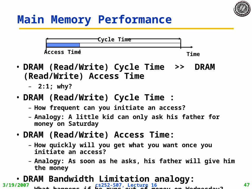
• DRAM (Read/Write) Cycle Time >> DRAM (Read/Write) Access Time
– 2:1; why?
• DRAM (Read/Write) Cycle Time :– How frequent can you initiate an access?– Analogy: A little kid can only ask his father for money on Saturday
• DRAM (Read/Write) Access Time:– How quickly will you get what you want once you initiate an access?– Analogy: As soon as he asks, his father will give him the money
• DRAM Bandwidth Limitation analogy:– What happens if he runs out of money on Wednesday?
TimeAccess Time
Cycle Time
Main Memory Performance

3/19/2007 cs252-S07, Lecture 16 48
Access Pattern without Interleaving:
Start Access for D1
CPU Memory
Start Access for D2D1 available
Access Pattern with 4-way Interleaving:
Acc
ess B
ank
0
Access Bank 1Access Bank 2
Access Bank 3We can Access Bank 0 again
CPU
MemoryBank 1
MemoryBank 0
MemoryBank 3
MemoryBank 2
Increasing Bandwidth - Interleaving

3/19/2007 cs252-S07, Lecture 16 49
• Simple: – CPU, Cache, Bus, Memory
same width (32 bits)
• Interleaved: – CPU, Cache, Bus 1 word:
Memory N Modules(4 Modules); example is word interleaved
• Wide: – CPU/Mux 1 word;
Mux/Cache, Bus, Memory N words (Alpha: 64 bits & 256 bits)
Main Memory Performance

3/19/2007 cs252-S07, Lecture 16 50
• Timing model– 1 to send address, – 4 for access time, 10 cycle time, 1 to send data– Cache Block is 4 words
• Simple M.P. = 4 x (1+10+1) = 48• Wide M.P. = 1 + 10 + 1 = 12• Interleaved M.P. = 1+10+1 + 3 =15
address
Bank 0
048
12
address
Bank 1
159
13
address
Bank 2
26
1014
address
Bank 3
37
1115
Main Memory Performance

3/19/2007 cs252-S07, Lecture 16 51
Avoiding Bank Conflicts
• Lots of banksint x[256][512];for (j = 0; j < 512; j = j+1)for (i = 0; i < 256; i = i+1)x[i][j] = 2 * x[i][j];
• Even with 128 banks, since 512 is multiple of 128, conflict on word accesses
• SW: loop interchange or declaring array not power of 2 (“array padding”)
• HW: Prime number of banks– bank number = address mod number of banks– bank number = address mod number of banks– address within bank = address / number of words in bank– modulo & divide per memory access with prime no. banks?

3/19/2007 cs252-S07, Lecture 16 52
Finding Bank Number and Address within a bank
Problem: We want to determine the number of banks, Nb, to useand the number of words to store in each bank, Wb, such that:
• given a word address x, it is easy to find the bank where x will be found, B(x), and the address of x within the bank, A(x).
• for any address x, B(x) and A(x) are unique.
• the number of bank conflicts is minimized

3/19/2007 cs252-S07, Lecture 16 53
Finding Bank Number and Address within a bank
Solution: We will use the following relation to determine the banknumber for x, B(x), and the address of x within the bank, A(x):
B(x) = x MOD NbA(x) = x MOD Wb
and we will choose Nb and Wb to be co-prime, i.e., there is no primenumber that is a factor of Nb and Wb (this condition is satisfiedif we choose Nb to be a prime number that is equal to an integerpower of two minus 1). We can then use the Chinese Remainder Theorem to show that B(x) and A(x) is always unique.

3/19/2007 cs252-S07, Lecture 16 54
• Chinese Remainder TheoremAs long as two sets of integers ai and bi follow these rules
and that ai and aj are co-prime if i j, then the integer x has only one solution (unambiguous mapping):
– bank number = b0, number of banks = a0 – address within bank = b1, number of words in bank = a1
– N word address 0 to N-1, prime no. banks, words power of 2
• 3 banks Nb = 3, and 8 words per bank, Wb = 8.
bi xmodai,0 bi ai, 0 x a0 a1a2
Fast Bank Number
Seq. Interleaved Modulo InterleavedBank Number: 0 1 2 0 1 2
Address within Bank: 0 0 1 2 0 16 8
1 3 4 5 9 1 172 6 7 8 18 10 23 9 10 11 3 19 114 12 13 14 12 4 205 15 16 17 21 13 56 18 19 20 6 22 147 21 22 23 15 7 23

3/19/2007 cs252-S07, Lecture 16 55
Fast Memory Systems: DRAM specific
• Multiple CAS accesses: several names (page mode)– Extended Data Out (EDO): 30% faster in page mode
• New DRAMs to address gap; what will they cost, will they survive?
– RAMBUS: startup company; reinvent DRAM interface» Each Chip a module vs. slice of memory» Short bus between CPU and chips» Does own refresh» Variable amount of data returned» 1 byte / 2 ns (500 MB/s per chip)
– Synchronous DRAM: 2 banks on chip, a clock signal to DRAM, transfer synchronous to system clock (66 - 150 MHz)
– Intel claims RAMBUS Direct (16 b wide) is future PC memory
• Niche memory or main memory?– e.g., Video RAM for frame buffers, DRAM + fast serial output

3/19/2007 cs252-S07, Lecture 16 56
Fast Page Mode Operation• Regular DRAM Organization:
– N rows x N column x M-bit– Read & Write M-bit at a time– Each M-bit access requires
a RAS / CAS cycle• Fast Page Mode DRAM
– N x M “SRAM” to save a row• After a row is read into the
register– Only CAS is needed to access
other M-bit blocks on that row– RAS_L remains asserted while
CAS_L is toggled
N ro
ws
N cols
DRAM
ColumnAddress
M-bit OutputM bits
N x M “SRAM”
RowAddress
A Row Address
CAS_L
RAS_L
Col Address Col Address
1st M-bit Access
Col Address Col Address
2nd M-bit 3rd M-bit 4th M-bit

3/19/2007 cs252-S07, Lecture 16 57
• Tunneling Magnetic Junction RAM (TMJ-RAM)– Speed of SRAM, density of DRAM, non-volatile (no refresh)– “Spintronics”: combination quantum spin and electronics– Same technology used in high-density disk-drives
Something new: Structure of Tunneling Magnetic Junction

3/19/2007 cs252-S07, Lecture 16 58
MEMS-based Storage• Magnetic “sled” floats
on array of read/write heads
– Approx 250 Gbit/in2
– Data rates:IBM: 250 MB/s w 1000 headsCMU: 3.1 MB/s w 400 heads
• Electrostatic actuators move media around to align it with heads
– Sweep sled ±50m in < 0.5s
• Capacity estimated to be in the 1-10GB in 10cm2
See Ganger et all: http://www.lcs.ece.cmu.edu/research/MEMS

3/19/2007 cs252-S07, Lecture 16 59
• Motivation:– DRAM is dense Signals are easily disturbed– High Capacity higher probability of failure
• Approach: Redundancy– Add extra information so that we can recover from errors– Can we do better than just create complete copies?
• Block Codes: Data Coded in blocks– k data bits coded into n encoded bits– Measure of overhead: Rate of Code: K/N – Often called an (n,k) code– Consider data as vectors in GF(2) [ i.e. vectors of bits ]
• Code Space is set of all 2n vectors, Data space set of 2k vectors
– Encoding function: C=f(d)– Decoding function: d=f(C’)– Not all possible code vectors, C, are valid!
Big storage (such as DRAM/DISK):Potential for Errors!

3/19/2007 cs252-S07, Lecture 16 60
Need for Error Correction!• Motivation:
– Failures/time proportional to number of bits!– As DRAM cells shrink, more vulnerable
• Went through period in which failure rate was low enough without error correction that people didn’t do correction
– DRAM banks too large now– Servers always corrected memory systems
• Basic idea: add redundancy through parity bits– Common configuration: Random error correction
» SEC-DED (single error correct, double error detect)» One example: 64 data bits + 8 parity bits (11% overhead)
– Really want to handle failures of physical components as well» Organization is multiple DRAMs/DIMM, multiple DIMMs» Want to recover from failed DRAM and failed DIMM!» “Chip kill” handle failures width of single DRAM chip
3/19/2007 cs252-S07, Lecture 16 61
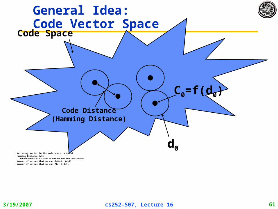
• Not every vector in the code space is valid• Hamming Distance (d):
– Minimum number of bit flips to turn one code word into another• Number of errors that we can detect: (d-1)• Number of errors that we can fix: ½(d-1)
Code Space
d0
C0=f(d0)Code Distance
(Hamming Distance)
General Idea:Code Vector Space

3/19/2007 cs252-S07, Lecture 16 62
Conclusion• Memory wall inspires optimizations since so much
performance lost there– Reducing hit time: Small and simple caches, Way prediction,
Trace caches– Increasing cache bandwidth: Pipelined caches, Multibanked
caches, Nonblocking caches– Reducing Miss Penalty: Critical word first, Merging write buffers– Reducing Miss Rate: Compiler optimizations– Reducing miss penalty or miss rate via parallelism: Hardware
prefetching, Compiler prefetching
• “Auto-tuners” search replacing static compilation to explore optimization space?