Standard Operating Procedure I - ywcmatsci.yale.edu MCC SEM SOP v1_7.pdf · Version 1.7, May 2018 ....
33
Version 1.7, May 2018 Standard Operating Procedure I: SEM, BSE and STEM ywcmatsci.yale.edu ESC II, Room A119F 810 West Campus Drive West Haven, CT 06516
Transcript of Standard Operating Procedure I - ywcmatsci.yale.edu MCC SEM SOP v1_7.pdf · Version 1.7, May 2018 ....

Version 1.7, May 2018
Standard Operating Procedure I: SEM, BSE and STEM
ywcmatsci.yale.edu
ESC II, Room A119F 810 West Campus Drive West Haven, CT 06516

Hitachi SU8230 SEM
1
Yale West Campus Materials Characterization Core

Hitachi SU8230 SEM
1
Yale West Campus Materials Characterization Core
> FOLLOW the SOP strictly to keep the instrument in good condition. Any violation will lead to user account suspension.
> NEVER use your own USB drive on instrument computer. Data can be transferred with the Jump Drive provided by the Core.
> NEVER surf the web on the instrument computer to minimize the risk of the computer being hacked.
> NEVER allow other users to get access to instrument computer on your reservation.
> REPORT any issues to Core director immediately so they can be fixed on time.

Hitachi SU8230 SEM
2
Yale West Campus Materials Characterization Core

Hitachi SU8230 SEM
1
Yale West Campus Materials Characterization Core
Table of Contents 1 Introduction ............................................................................................................................. 1
2 Specimen Preparation ............................................................................................................. 2
3 Starting Instrument .................................................................................................................. 3
4 System Status Check ............................................................................................................... 4
5 Loading the Specimen............................................................................................................. 7
6 Image Observation ................................................................................................................ 10
7 Closing SEM measurement................................................................................................... 19
8 Checklist after Experiment ................................................................................................... 20
9 Photodiode Back Scattered Electron (PD-BSE) ................................................................... 21
10 Scanning Transmission Electron Microscopy (STEM) ........................................................ 24

Hitachi SU8230 SEM
1
Yale West Campus Materials Characterization Core

Hitachi SU8230 SEM
1
Yale West Campus Materials Characterization Core
Hitachi SU8230 Standard Operating Procedure 1 Introduction
1) Instrument features: > Cold field emission (CFE) e-beam source: high resolution on conductive surfaces (0.8
nm on Au clusters/magnetic tape) > Sliding-in annular Energy Dispersive Spectroscopy (EDS) detector: high elemental
mapping resolution > Sliding-in annular Photo Diode PD-BSE detector: high signal intensity from
backscattered electron > Scanning Transmission Electron Microscopy (STEM) detector: high resolution
compositional contrast imaging, ideal for EDS mapping 2) Location
Materials Characterization Core Room A119 810 West Campus Drive West Haven, CT 06516
3) Primary Staff Contact
Dr. Min Li Tel: 203-737-8270 Email: [email protected] Office: ESC II, Room A119D
Zishan Wu, Lab Assistant [email protected] 203-824-5563 (cell) Office: ESC II
Yiren Zhong, Lab Assistant [email protected] 203-710-9820 (cell)
The Yale West Campus MCC Facilities are operated for the benefit of all researchers. If you encounter any problems with this facility, please contact the staff member listed above immediately. There is never a penalty for asking questions. If the equipment is not behaving exactly the way it should, contact a staff member.
Warning: Please follow strictly the SOP to keep the facility at good condition. We DO NOT recommend user explorations on program unless endorsed by core director.

Hitachi SU8230 SEM
2
Yale West Campus Materials Characterization Core
2 Specimen Preparation1 1) Always wear gloves for vacuum sample preparation!! Change gloves if touched computer
keyboard and mouse. 2) The sample for SEM needs to be completely dried!
a) The powders samples can be dripped and dried on Si substrate. Alternately, powders can be sprinkled on Conducting Graphite Paint (supplied in the Core) directly applied on the specimen stub, or on to double sided conducting carbon tape. Note: • Do not press powders too hard as it may change surface morphology. • The Conducting Graphite Paint is highly recommended to fix the samples
especially magnetic particles for high magnification (>100 k) measurement. b) The solid samples, large size flakes, single crystals can be fixed directly onto the
sample holder using Conducting Graphite Paint.
3) Attach the specimen stub to the specimen holder; DO NOT overtighten the locking ring. 4) Adjust the height of specimen so that the highest point on the sample matches the lower
surface of the height gauge (see photo below).
Warning: Samples mounted above the dashed line will crash into the lens system or detectors (EDS, STEM), and the repair fee will be charged to PI’s account.)
5) Clean sample holder: bring the specimen stub inside the fume hood and blow off loose particles on the sample surface using the N2 gun.2
1 Always wear gloves for your sample preparation in your own lab or in MCC! Warnings will be given for violations and the user account will be revoked after three warnings with notice to PI. Further training at PI’s expense will be required to resume the account. 2 This step is crucial to keep the SEM chamber vacuum at good pressure, which in turn improves the imaging resolution with less surface contamination and keeps the SEM lens system at good condition.
Specimen stub
Locking ring
Specimen holder
Hitachi SU8230 SEM
3
Yale West Campus Materials Characterization Core
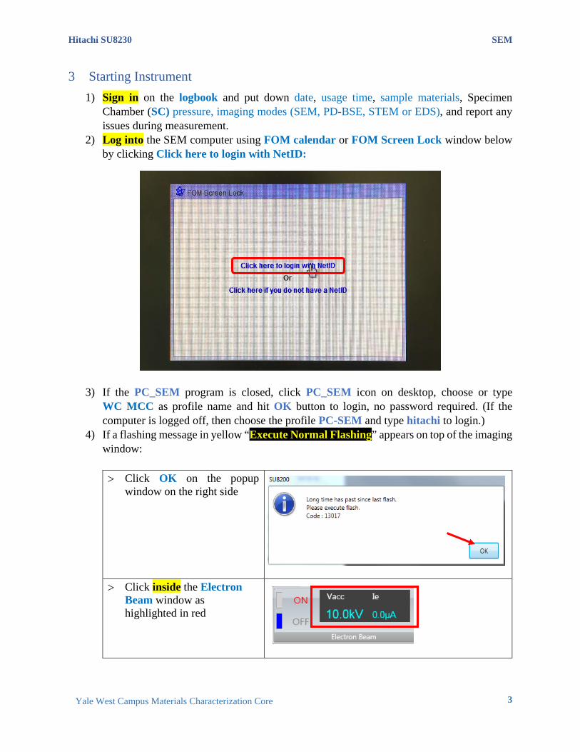
3 Starting Instrument 1) Sign in on the logbook and put down date, usage time, sample materials, Specimen
Chamber (SC) pressure, imaging modes (SEM, PD-BSE, STEM or EDS), and report any issues during measurement.
2) Log into the SEM computer using FOM calendar or FOM Screen Lock window below by clicking Click here to login with NetID:
3) If the PC_SEM program is closed, click PC_SEM icon on desktop, choose or type
WC MCC as profile name and hit OK button to login, no password required. (If the computer is logged off, then choose the profile PC-SEM and type hitachi to login.)
4) If a flashing message in yellow “Execute Normal Flashing” appears on top of the imaging window: > Click OK on the popup
window on the right side
> Click inside the Electron
Beam window as highlighted in red

Hitachi SU8230 SEM
4
Yale West Campus Materials Characterization Core
> Click button in the popup Vacc (accelerating voltage) and Ie (emission current) setting window:
> Click Execute button highlighted in the Flashing window below to flash the tip.
> Click Close button in the popup Vacc and Ie setting window
4 System Status Check 1) Check building supplied Compressed Air (CA) and Nitrogen (N2) pressure on the wall,
make sure the CA pressure reads around 80 psi and N2 around 2 psi. If both gauges read zero, contact Core Manager immediately. Warning: Operating without compressed air and nitrogen will lead to system damage.

Hitachi SU8230 SEM
5
Yale West Campus Materials Characterization Core
2) Check the Electron Beam window below:
> The accelerating voltage Vacc should be OFF with a solid blue bar highlighted by arrow. If Vacc is ON, click the OFF button to turn the beam off.
3) Turn on the small LCD on the table by pressing the switch at the top left corner in the
back. This unit includes the Specimen Chamber (SC) camera display and the camera power supply.
> Check and make sure the specimen stage is at the exchange EXC position and NO sample holders on it, as highlighted in the picture below:
> Check and make sure no other detectors (PD-BSE or EDS) underneath the SEM column, as highlighted in the picture below:
4) Check and make sure the PD-BSE, STEM and EDS detectors are fully retracted on the
left side of SEM chamber:
Empty specimen stage at EXC position
SEM column
No detector
CA ~ 80 psi
N2 ~ 2 psi

Hitachi SU8230 SEM
6
Yale West Campus Materials Characterization Core
5) Check to make sure the Specimen Chamber SC pressure is at LE-4 Pascal.
6) Check to make sure that the LN2 level in the dewar attached to SEM SC chamber as highlighted is high enough to support the measurement. A full tank can support ~1 hour. Warning: momentarily check the LN2 level to prevent sudden outgassing inside chamber which will lead to pressure burst above 10-3 Pa and beam shutdown3
3 Note: this step is highly recommended for high magnifications >100 k or low accelerating voltages < 1 kV.
Dewar
Fully retracted
Fully retracted
Fully retracted
PD-BSE
BF-STEM
EDS
Hitachi SU8230 SEM
7
Yale West Campus Materials Characterization Core
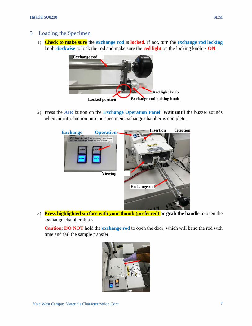
5 Loading the Specimen 1) Check to make sure the exchange rod is locked. If not, turn the exchange rod locking
knob clockwise to lock the rod and make sure the red light on the locking knob is ON.
2) Press the AIR button on the Exchange Operation Panel. Wait until the buzzer sounds
when air introduction into the specimen exchange chamber is complete.
3) Press highlighted surface with your thumb (preferred) or grab the handle to open the exchange chamber door.
Caution: DO NOT hold the exchange rod to open the door, which will bend the rod with time and fail the sample transfer.
Exchange Operation
Insertion detection
Viewing
Exchange rod
Exchange rod locking knob Red light knob
Exchange rod
Locked position
Hitachi SU8230 SEM
8
Yale West Campus Materials Characterization Core
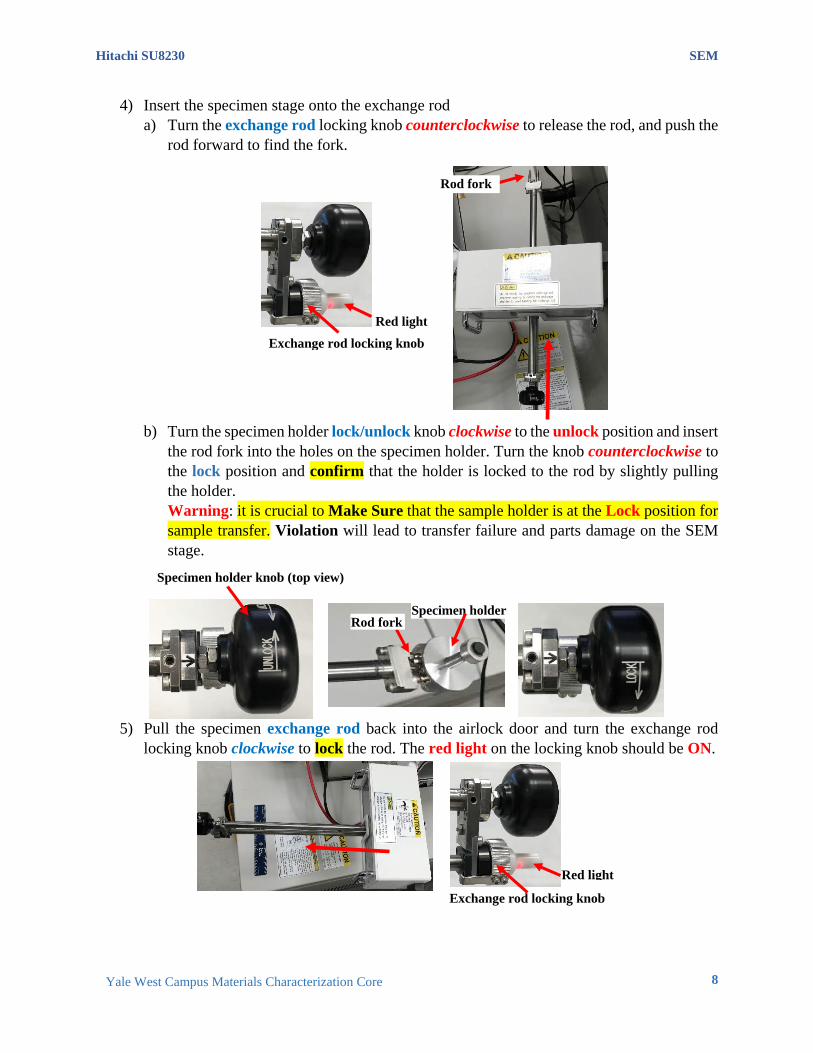
4) Insert the specimen stage onto the exchange rod a) Turn the exchange rod locking knob counterclockwise to release the rod, and push the
rod forward to find the fork.
b) Turn the specimen holder lock/unlock knob clockwise to the unlock position and insert the rod fork into the holes on the specimen holder. Turn the knob counterclockwise to the lock position and confirm that the holder is locked to the rod by slightly pulling the holder. Warning: it is crucial to Make Sure that the sample holder is at the Lock position for sample transfer. Violation will lead to transfer failure and parts damage on the SEM stage.
5) Pull the specimen exchange rod back into the airlock door and turn the exchange rod locking knob clockwise to lock the rod. The red light on the locking knob should be ON.
Specimen holder knob (top view)
Specimen holder Rod fork
Exchange rod locking knob
Red light
Rod fork
Exchange rod locking knob
Red light

Hitachi SU8230 SEM
9
Yale West Campus Materials Characterization Core
6) Close and hold exchange chamber door and press the EVAC button on the exchange operation panel. Wait until the buzzer sounds indicating the chamber is evacuated back into vacuum Caution: DO NOT hold the exchange rod to close the door as this will lead to rod bending with time.
7) Press OPEN button on the exchange operation panel. Wait until the buzzer sounds and the gate valve is open.
8) Turn the exchange rod locking knob counterclockwise to release the lock. Push the transfer
rod forward slowly into specimen chamber until the insertion detection lamp on top of the exchange chamber is lit in blue. Warning:
> DO NOT rotate the specimen holder knob while pushing the rod into specimen chamber. This may cause accidental switch of Lock position to Unlock on the rod leading to sample transfer failure and mechanic damage.
> Always hold the knob when pushing the transfer forward to prevent rod accidental sliding into specimen chamber.
9) Turn the specimen holder knob clockwise to UNLOCK position. With left hand holding the door, right hand grabs the knob and slowly pushes against glass window with
Exchange Operation Panel
Exchange rod locking knob Red light
Specimen holder knob
Insertion detection lamp

Hitachi SU8230 SEM
10
Yale West Campus Materials Characterization Core
knuckles and pull the rod all the way to the back and turn exchange rod locking knob clockwise to lock the rod. The red light on the locking knob should be ON.
10) Press the CLOSE button on the exchange operation panel and wait until the buzzer sounds, indicating the sample transfer is complete.
6 Image Observation
1) Click the HOME button on the menu at the top right of PC-SEM window (Caution: DO NOT repeatedly click this button as this may lead to STOP button next ineffective) and watch the sample holder moving in the specimen chamber scope LCD from the exchange EXC position to HOME (measurement) position underneath the electron column.
2) Click Set button in the Stage tab to set the specimen stub Size and Height
3) In the popup window below
a) Choose the Size of specimen stub one size up for safety purpose, e.g.: choose 2 inches for 1 inch specimen stub).4
b) Set Height to Standard.
4 Failure to follow the instruction may lead to severe damage to the lens system; the user account will be revoked and the repair fee will be charged to PI’s account.
a) b) c)

Hitachi SU8230 SEM
11
Yale West Campus Materials Characterization Core
Warning: make sure the specimen stub has been carefully aligned using height gauge.
c) Confirm that the boxes next to additional detectors (EDX, BSE, BF-STEM and FQ-EDX) are not checked.
4) Setting imaging parameters. a) Confirm the accelerating voltage Vacc is OFF in the Electron Beam window
below.
b) Set accelerating voltage Vacc: > Click inside Electron Beam window in highlighted rectangle region
above and choose Vacc from dropdown list. (typical values: 1kV, 5 kV, 10kV or 15kV)
Warning: > Do Not type arbitrary numbers, as the beams from dropdown list have been
calibrated by service engineer. > Always try small voltage first to avoid surface damage, over-charging and
ebeam induced carbon deposition (black imaging box) c) Set emission current Ie:
> Click inside Electron Beam window above to choose Ie at 10 µA. Note:
> Consider smaller values if surface charging or carbon deposition is a concern.
d) Confirm the LM (Lower Magnification mode) is active inside Magnification
window below. If not, click to switch back to LM mode.
e) Choose Rapid Scan Mode in the window below to start with.
Hitachi SU8230 SEM
12
Yale West Campus Materials Characterization Core
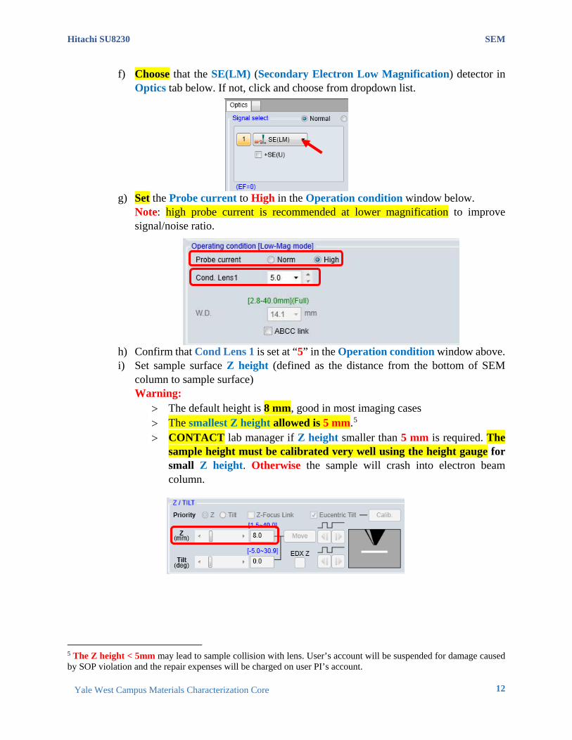
f) Choose that the SE(LM) (Secondary Electron Low Magnification) detector in Optics tab below. If not, click and choose from dropdown list.
g) Set the Probe current to High in the Operation condition window below. Note: high probe current is recommended at lower magnification to improve signal/noise ratio.
h) Confirm that Cond Lens 1 is set at “5” in the Operation condition window above. i) Set sample surface Z height (defined as the distance from the bottom of SEM
column to sample surface) Warning:
> The default height is 8 mm, good in most imaging cases > The smallest Z height allowed is 5 mm.5 > CONTACT lab manager if Z height smaller than 5 mm is required. The
sample height must be calibrated very well using the height gauge for small Z height. Otherwise the sample will crash into electron beam column.
5 The Z height < 5mm may lead to sample collision with lens. User’s account will be suspended for damage caused by SOP violation and the repair expenses will be charged on user PI’s account.

Hitachi SU8230 SEM
13
Yale West Campus Materials Characterization Core
Warning: To avoid sample collision with detectors, always check the table below before changing Z height value
5) Check and Confirm the Specimen Chamber (SC) pressure has reached LE-4 Pascal on EVAC CONTROL panel as highlighted below.6
6) Click the ON button to turn on beam voltage Vacc in the Electron Beam window below:
Note: the process takes seconds, please be patient and wait till the popup window disappears.
7) Click on the top menu bar or AUTO button on the Manual Operation Panel below if the image is too bright or dark. The BIRGHTNESS and CONTRAST knobs can be used separately for manual adjustment.
6 Turning on beam too early will cause electron gun chamber contamination and downgrade the SEM performance eventually.
Z height setting restrictions (Severe damage to lens may happen with z < 5 mm): Regular SEM: 5 – 20 mm EDS: 11 – 20 mm PD-BSE: 8 – 20 mm BF-STEM: 5 – 20 mm

Hitachi SU8230 SEM
14
Yale West Campus Materials Characterization Core
8) Roll the track ball on the STAGE CONTROLLER to find the field of interested in LM mode:
9) Adjust magnification using MAGNIFICATION knob on the Manual Operation Panel. 10) Adjust focus using FOCUS COARSE and FINE knobs. Move the stage to look for the
field of interest in LM mode, and then click to switch to High Magnification (HM) mode.
11) In HM mode, change the magnification and adjust imaging quality using FOCUS and STIGMA X/Y knobs on Manual Operation Panel
a) If image drifts (swaying or heaving) during focusing: > Click Alignment tab and click
Beam Align button. The ALIGNMENT LED on the Manual Operation Panel should be flashing.
Manual Operation Panel

Hitachi SU8230 SEM
15
Yale West Campus Materials Characterization Core
> Bring the circular image to the center of the image area by adjusting X and Y knobs on the panel.
> Click Aperture Align button below
and adjust STIGMA/ALIGNMENT X /Y knobs on the panel to minimize the wobbling motion in image.
> Click Stigma Align X button below and adjust STIGMA/ALIGNMENT X /Y knobs to minimize the wobbling motion in image. Repeat similar adjustment on by clicking Stigma Align Y button. (Note: reduce Magnification below 50k for this step)
> Click on Alignment tab. Make sure the Alignment LED on Manual Operation Panel is OFF
b) If image distorts (stretching), correct astigmatism:
> Make sure the Stigma LED on Manual Operation Panel is ON. Use the STIGMA/ALIGNMENT X/Y knobs alternating with FINE FOCUS knob to reduce distortion and obtain the sharpest image.
c) Repeat steps a) and b) if necessary when switched to higher magnification. 12) Save image:
a) Select the field of view, confirm image with slow scan or .

Hitachi SU8230 SEM
16
Yale West Campus Materials Characterization Core
b) Click the Capture button .
c) Click button next to to resume live image scan. 13) Image capture settings for charging samples (image distorts, streaky, drifts during scan):
a) Choose CSS (Charge Suppressed Scan) mode: > Clicking on the small box in the Scan Menu to open the Scan Button Setting
window.
> Check the radio button next to CSS. Hit Apply button and Close in the
window below:
> The CSS Scan menu should appear as follows:
Hitachi SU8230 SEM
17
Yale West Campus Materials Characterization Core
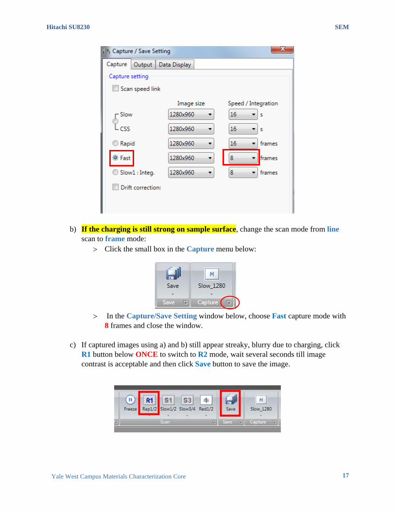
b) If the charging is still strong on sample surface, change the scan mode from line
scan to frame mode: > Click the small box in the Capture menu below:
> In the Capture/Save Setting window below, choose Fast capture mode with 8 frames and close the window.
c) If captured images using a) and b) still appear streaky, blurry due to charging, click
R1 button below ONCE to switch to R2 mode, wait several seconds till image contrast is acceptable and then click Save button to save the image.

Hitachi SU8230 SEM
18
Yale West Campus Materials Characterization Core
14) Data save: a) Click ALL button on the bottom of the image thumbnail column below:
b) Click PCI button in above window, the collected images will be transferred into
Quartz PCI program below. Click File in the menu and select Export All… on the dropdown menu, then Browse to choose Export to Path and File Format and hit OK.

Hitachi SU8230 SEM
19
Yale West Campus Materials Characterization Core
7 Closing SEM measurement 1) Click the OFF button to turn off electron beam in the Electron Beam window below:
2) Click inside Electron Beam window above in highlighted rectangle region and set beam voltage (Vacc) to 10 kV, and emission current Ie to 10 µA
3) If Deceleration Mode was used, change back to regular mode 4) Switch imaging mode to Lower Magnification (LM) Mode
5) Click the EXC button on PC-SEM software top menu to move the specimen stage to the exchange position.
6) Check and confirm in Stage > Set: Set Sample Size/Detectors window below that all detector check boxes are unchecked.
7) Unloading samples from the specimen chamber: following the reversed order from
sample loading, check Section 5, steps 1) to 10). 8) Turn off the small LCD below SEM computer monitor (SC chamberscope LCD). 9) DO NOT close or minimize PC-SEM program 10) Use ONLY the Core USB flash drive for data transfer. 11) Log off FOM from SEM computer or user’s FOM SEM calendar. Make sure the
following FOM Screen Lock window with dark background appear on the monitor to stop being continuously charged. Note: if reporting issues, please check “Something wrong” in FOM logoff window and describe the issues in the empty box below.

Hitachi SU8230 SEM
20
Yale West Campus Materials Characterization Core
8 Checklist after Experiment 1) Sign off logbook. 2) Remove samples from the stub on the specimen holder, and clean the holder with
Kimwipes using IPA. Warning: Do Not dissemble the specimen holder.
3) Store the specimen holder in assigned organizer box. 4) Clear the SEM work bench.
Warning: failed to follow checklist twice in one month will lead to temporary account suspension.

Hitachi SU8230 SEM
21
Yale West Campus Materials Characterization Core
9 Photodiode Back Scattered Electron (PD-BSE) 1) Make sure Vacc is OFF 2) In PC_SEM program with the sample holder at EXC or HOME position, click Set button
in the Stage tab and check the BSE box
3) To AVOID damages to detectors, choose Z range: 8-20 mm, typically 8 mm
4) Select Vacc at 15 kV and regular Ie=10 µA as the PD-BSE requires high e-beam kV 5) Select Dual Screen mode on the PC_SEM top menu bar, and choose detector
for the first screen and detector the second
6) Switch to LM mode and turn Vacc ON 7) Make sure sample Z height is between 8mm and 20 mm 8) Slowly move the PD-BSE detector to the measurement position
Caution: > Slow detector motion helps minimizing the vibrations from both detector and SC
chamber, stop moving quickly once stopped 9) Monitor the movement of PD-BSE detector until it stops between sample and lens on
chamber scope LCD screen and then TURN OFF LCD screen Warning: the PD-BSE detector is very sensitive to ambient light; the LCD screen must be turned off before PD-BSE imaging

Hitachi SU8230 SEM
22
Yale West Campus Materials Characterization Core
10) Click beside to activate SE imaging: a) Find interested areas on the sample inside the annular PD-BSE detector in LM
mode; adjust focus and switch to HM mode. b) Get a GOOD image in HM mode
Caution: Always switch to SE window to adjust image quality for PD-BSE imaging
11) Click beside to activate BSE imaging:
a) Click or AUTO button on the Manual Operation Panel to adjust the image brightness/contrast. The BIRGHTNESS and CONTRAST knobs can be used separately to do manual adjustment
b) Select the field of view, confirm image with slow scan or and then,
click the Capture button .
Notice: do not use rapid scan mode for PD-BSE imaging 12) To quit PD-BSE detection mode:
a) Switch to LM mode b) In PC_SEM program, click the OFF button to turn off Vacc
c) Turn the chamber scope LCD ON d) Crank to fully retract the PD-BSE detector e) Click the EXC button to move the specimen stage to the exchange position. Wait until
the flashing green signal bar becomes solid next to EXC button.
f) Click Set button in the Stage tab; uncheck BSE(PD) box, and then follow Section 7
Closing SEM measurement and 8 Checklist after Experiment to close the measurement.

Hitachi SU8230 SEM
23
Yale West Campus Materials Characterization Core

Hitachi SU8230 SEM
24
Yale West Campus Materials Characterization Core
10 Scanning Transmission Electron Microscopy (STEM) Notice: The STEM sample holder has a standard height of 36 mm, so NO Height Gauge is
required.
1) Make sure Vacc is OFF 2) In PC_SEM program with the sample holder at EXC or HOME position, click Set button
in the Stage tab and check the BF-STEM (Bright Field) box
3) To AVOID damages to STEM detector, choose Z range: 8-20 mm, typically 8 mm 4) Select Vacc ≤ 20 kV and regular Ie=10 µA in STEM
5) Select Dual Screen mode on the PC_SEM top menu bar, and choose detector for the first screen and detector the second
6) Switch to LM mode and turn Vacc ON 7) Make sure the Z ≤ 20 mm, slowly move the STEM detector to the measurement position
above sample Caution: moving slowly prevents the vibrations of detector and SC chamber, stop moving once feel stopped
8) Click beside to activate SE imaging: a) Find interested areas on the sample in LM mode; adjust focus and switch to HM
mode.
Hitachi SU8230 SEM
25
Yale West Campus Materials Characterization Core
b) Following instructions in Section 6 Image Observation to get a well focused image in HM mode Caution: Always switch to SE window to adjust image quality for STEM imaging
9) Click beside to activate STEM imaging:
a) Click or AUTO button on the Manual Operation Panel to adjust the image brightness/contrast. The BIRGHTNESS and CONTRAST knobs can be used separately to do manual adjustments
b) Select the field of view, confirm image with slow scan or and then,
click the Capture button .
Notice: do not use rapid scan mode for STEM imaging 10) To quit STEM detection mode:
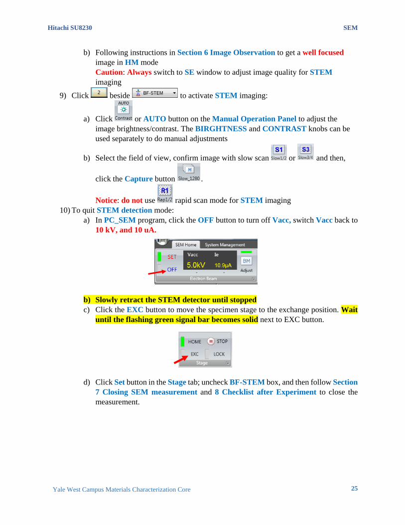
a) In PC_SEM program, click the OFF button to turn off Vacc, switch Vacc back to 10 kV, and 10 uA.
b) Slowly retract the STEM detector until stopped c) Click the EXC button to move the specimen stage to the exchange position. Wait
until the flashing green signal bar becomes solid next to EXC button.
d) Click Set button in the Stage tab; uncheck BF-STEM box, and then follow Section
7 Closing SEM measurement and 8 Checklist after Experiment to close the measurement.

Hitachi SU8230 SEM
26
Yale West Campus Materials Characterization Core

Hitachi SU8230 SEM
27
Yale West Campus Materials Characterization Core