HD44780U (LCD-II), (Dot Matrix Liquid Crystal Display Controller ...
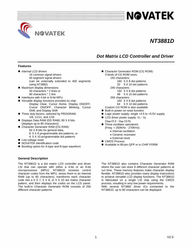
NT3881D
Dot Matrix LCD Controller and Driver
1 V2.5
Features ! Internal LCD drivers 16 common signal drivers 40 segment signal drivers (can be externally extended to 400 segments using NT3882) ! Maximum display dimensions 40 characters * 2 lines or 80 characters * 1 line ! Interfaces with 4-bit or 8-bit MPU ! Versatile display functions provided on chip: Display Clear, Cursor Home, Display ON/OFF, Cursor ON/OFF, Character Blinking, Cursor Shift, and Display Shift ! Three duty factors, selected by PROGRAM: 1/8, 11/11, and 1/16 ! Displays Data RAM (DD RAM): 80 X 8 bits (displays up to 80 characters) ! Character Generator RAM (CG RAM): 64 X 8 bits for general data, 8 5 X 8 programmable dot patterns, or 4 5 X 10 programmable dot patterns ! Low voltage reset ! NOVATEK Identification code ! Bonding option for A-type and B-type waveform
! Character Generator ROM (CG ROM): 3 kinds of CG ROM sizes: 192 characters: 160 5 X 8 dot patterns 32 5 X 10 dot patterns 240 characters: 192 5 X 8 dot patterns 48 5 X 10 dot patterns 256 characters: 192 5 X 8 dot patterns 64 5 X 10 dot patterns Custom CG ROM is also available ! Built-in power-on reset function ! Logic power supply: single +4.5 to +5.5V supply ! LCD driver power supply: V1 - V5 (VDD+0.3 - VDD-13.5) ! Three oscillator operations (Freq. = 250KHz - 270KHz): • Internal oscillation • Ceramic resonator • External clock ! CMOS Process ! Available in 80-pin QFP or in CHIP FORM
General Description The NT3881D is a dot matrix LCD controller and driver LSI that can operate with either a 4-bit or an 8-bit microprocessor (MPU). NT3881D receives control character codes from the MPU, stores them in an internal RAM (up to 80 characters), transforms each character code into a 5 X 7, 5 X 8, or 5 X 10 dot matrix character pattern, and then displays the codes on the LCD panel. The built-in Character Generator ROM consists of 256 different character patterns.
The NT3881D also contains Character Generator RAM where the user can store 8 different character patterns at run time. These memory features make character display flexible. NT3881D also provides many display instructions to achieve versatile LCD display functions. The NT3881D is fabricated on a single LSI chip using the CMOS process, resulting in very low power requirements. With several NT3882 driver ICs connected to the NT3881D, up to 80 characters can be displayed.

NT3881D
2 V2.5
Pin Configuration
``UM3881DFNT3881DF
SEG21
SEG20
SEG19
SEG18
SEG17
SEG16
SEG15
SEG14
SEG13
SEG12
SEG11
SEG10
SEG9
SEG8
SEG7
SEG6
SEG5
SEG4
SEG3
SEG2
SEG1
GND
OSC1
SEG23
SEG24
SEG25
SEG26
SEG27
SEG28
SEG29
SEG30
SEG31
SEG32
SEG33
SEG34
SEG35
SEG36
SEG37
SEG38 DB1
DB0
E
R/W
RS
D
M
VDD
CL2
CL1
V5
V4
V3
V2
V1
OSC2
SEG22
SEG39
SEG40
COM16
COM15
COM14
COM13
COM12
COM11
COM10
COM9
COM8
COM7
COM6
COM5
COM4
COM3
COM2
COM1
DB7
DB6
DB5
DB4
DB3
DB2
64 63 62 61 60 59 58 57 56 55 54 53 52 51 50 49 48 47 46 45 44 43 42 41
65
66
67
68
69
70
71
72
73
74
75
76
77
78
79
80
1 2 3 4 5 6 7 8 9 10 11 12 13 14 15 16 17 18 19 20 21 22 23 24
40
39
38
37
36
35
34
33
32
31
30
29
28
27
26
25

NT3881D
3 V2.5
Pad Configuration
1
2
3
4
5
6
7
8
9
10
11
12
13
14
15
16
17
18
19
20
21
22
23
24
25 26 27 28 29 30 31 32 81 34 35 36 37 38 39 40
41
42
43
44
45
46
47
48
49
50
51
52
53
54
55
56
57
58
59
60
61
62
63
64
656768697071727374757677787980
NT3881DH
66
33
SEG22
SEG21
SEG20
SEG19
SEG18
SEG17
SEG16
SEG15
SEG14
SEG13
SEG12
SEG11
SEG10
SEG9
SEG8
SEG7
SEG6
SEG5
SEG4
SEG3
SEG2
SEG1
GND
OSC1
SEG39
SEG40COM16COM15COM14COM13COM12COM11COM10COM9
COM8
COM7
COM6
COM5
COM4
COM3
COM2
COM1
DB7
DB6
DB5
DB4
DB3
DB2
OSC2
V1
V2
V3
V4
V5
CL1
CL2
VDDA
M D RS
R/W
E DB0
DB1
VDDB
SEG23
SEG24
SEG25
SEG26
SEG27
SEG28
SEG29
SEG30
SEG31
SEG32
SEG33
SEG34
SEG35
SEG36
SEG37
SEG38

NT3881D
4 V2.5
Block Diagram
I/OBUTTER
INSTRUCTIONREGISTER
(IR)
ADDRESSCOUNTER
TIMINGGENERATOR
INSTRUCTION
DECODER
CUR50RADDRESSCOURTER
DISPLAY DATARAM
(DD RAM)80 X 8 BITS
BUSYFLAG(BF)
DATAREGISTER
(DR)
7
8 CURSOR/BLINK
CONTROLLER
16-BITSHIFT
REGISTER
COMMONSIGNALDRIVER
CHARACTERGENERATOR
RAM(CG RAM)
64 X 8 BITS
CHARACTERGENERATOR
ROM(CG ROM)
40-BITLATCH
CIRCUIT
SEGMENTSIGNALDRIVER
PARALLEL-TO-SERIALCONVERTER 40-BIT SHIFT REGISTER
7
55
78 8
40
DB7~DB4
4
4
DB3~DB040
16
MCL1CL2
COM1|
COM16
SEG1|
SEG40
D
OSC2
8
RS
R/W
E
8
V1
V2V3V4
V5
OSC1
GND
VDD
7 7
7 7
8
3
16

NT3881D
5 V2.5
Pin and Pad Descriptions
Pin and Pad No. Designation I/O External Connection Description
1 - 22 SEG22 - SEG1 O LCD panel Segment signal output pins
24, 25 OSC1, OSC2 Pins connected to resistor or ceramic filter for internal clock oscillation. For external clock operation, clock inputs to OSC1.
26 - 30 V1 - V5 P Power supply Power supply for LCD driver
31 CL1 O NT3882 Clock to latch serial data D sent to NT3882.
32 CL2 O NT3882 Clock to shift serial data D
33, 81 VDDB, VDDA P Power supply VDD: +5V A-Type waveform: VDD bond to VDDA B-Type waveform: VDD bond to VDDB
23 GND P Power supply GND: 0V
34 M O NT3882 Switch signal to convert LCD drive waveform to AC
35 D O NT3882 Character pattern data corresponding to each common signal is transmitted serially from this output. 0-Non selection, 1-selection.
36 RS I MPU Register select signal 0: Instruction register (write) Busy flag, address counter (read) 1: Data register (write, read)
37 R/W I MPU Read/Write control signal 0: Write 1: Read
38 E I MPU Read/Write start signal
39 - 42 DB0 - DB3 I/O MPU Lower 4 tri-state bi-directional data bus for transmitting data between MPU and NT3881D. Not used during 4-bit operation.
43 - 46 DB4 - DB7 I/O MPU Higher 4 tri-state bi-directional data bus for transmitting data between MPU and NT3881D. DB7 is also used as busy flag.
47 - 62 COM1 - COM16 O LCD panel Common signal output pins
63 - 80 SEG40 - SEG23 O LCD panel Segment signal output pins

NT3881D
6 V2.5
Functional Description The NT3881D is a dot-matrix LCD controller and driver LSI. It operates with either a 4-bit or an 8-bit microprocessor (MPU). The NT3881D receives both instructions and data from the MPU. Some instructions set operation modes, such as the function mode, data entry mode, and display mode; as well as some control LCD display functions, such as clear display, restore display, shift display, and cursor. Other instructions include read and write both data and addresses. All instructions allow users convenient and powerful functions to control the LCD dot-matrix displays. Data is written into and read from the Data Display RAM (DD RAM) or the Character Generator RAM (CG RAM). As display character codes, the data stored in the DD RAM decodes a set of dot-matrix character patterns that are built into the Character Generator ROM (CG ROM). The CG ROM, with many character patterns (up to 256 patterns), defines the character pattern fonts. The NT3881D regularly scans the character patterns through the segment drivers. The CG RAM stores character pattern fonts at run time if users intend to show character patterns that are not defined in the CG ROM. This feature makes character display flexible. Other unused bytes can be used as general-purpose data storage. The LCD driver circuit consists of 16 common signal drivers and 40 segment signal drivers allowing a variety of application configurations to be implemented. Additionally, the user can extend display size by cascading the segment driver LSI NT3882. The maximum display dimensions can be either 80 characters in a 1-line display or 40 characters in a 2-line display.
Character Generator ROM (CG ROM) The character generator ROM generates LCD dot character patterns from the 8-bit character pattern codes. The NT3881D provides 3 CG ROM configurations: 1. 192 Characters: The CG ROM contains 160 5 X 8 dot character patterns and 32 5 X 10 dot character patterns. An example is the NT3881D-01, in which the relation between the character codes and character patterns is shown in Table 1. The character codes from 00H to 0FH are used to get character patterns from the CG RAM. Character codes from 10H to 1FH and from 80H to 9FH map to full
character patterns. Character codes from E0H to FFH are assigned to generate 5 X 10 dot character patterns, and other codes are used to generate 5x8 dot character patterns. 2. 240 Characters: The CG ROM contains 192 5 X 8 dot character patterns and 48 5 X 10 dot character patterns. An example of this type is the NT3881D-02, in which the relation between the character codes and character patterns is shown in Table 2. The character codes from 00H to 0FH are used to get character patterns from the CG RAM. Character codes from 10H to 1FH and from E0H to FFH are assigned to generate 5 X 10 dot character patterns, and other codes to generate 5 X 8 dot character patterns. No null character pattern exists in this type. Note that the underlined cursor, displayed on the 8th duty may be obscure if the 8th row of a dot character pattern is coded. We recommend that users display the cursor in the blinking mode if they code 5x8 dot character patterns is their custom CG ROM. 3. 256 Characters: The CG ROM contains 192 5 X 8 dot character patterns and 64 5 X 10 dot character patterns. No adequate example is presented here. The only difference between this type and the just mentioned second type is that the character codes from 00H to 0FH get character patterns from the CG ROM rather than from the CG RAM. These character codes are assigned to generate 5 X 10 dot character patterns. In this application, the CG RAM would be employed as a general-purpose data storage. Custom character patterns are available by mask-programming ROM. For convenience of character pattern development, NOVATEK has developed a user-friendly editor program for the NT3881D to help determine the character patterns users prefer. By executing the program on the computer, users can easily create and modify their character patterns. By transferring the resulting files generated by the program through a modem or some other communication method, the user and NOVATEK have established a reliable, fast link for programming the CG ROM.
NT3881D
7 V2.5
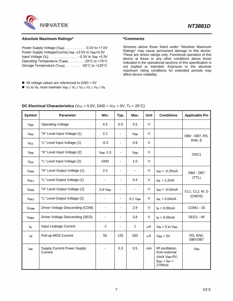
Absolute Maximum Ratings* Power Supply Voltage (VDD) . . . . . . . . . . -0.3V to +7.0V Power Supply Voltage(V1toV5).VDD -13.5V to VDD+0.3V Input Voltage (VI) . . . . . . . . . . . . . . . -0.3V to VDD +0.3V Operating Temperature (TOPR) . . . . . . . . -20°C to +75°C Storage Temperature (TSTG) . . . . . . . -55°C to +125°C
*Comments Stresses above those listed under "Absolute Maximum Ratings" may cause permanent damage to this device. These are stress ratings only. Functional operation of this device at these or any other conditions above those indicated in the operational sections of this specification is not implied or intended. Exposure to the absolute maximum rating conditions for extended periods may affect device reliability.
! All voltage values are referenced to GND = 0V ! V1 to V5, must maintain VDD ≥ V1 ≥ V2 ≥ V3 ≥ V4 ≥ V5.
DC Electrical Characteristics (VDD = 5.0V, GND = VEE = 0V, TA = 25°C)
Symbol Parameter Min. Typ. Max. Unit Conditions Applicable Pin
VDD Operating Voltage 4.5 5.0 5.5 V
VIH1 "H" Level Input Voltage (1) 2.2 - VDD V DB0 - DB7, RS,
VIL1 "L" Level Input Voltage (1) -0.3 - 0.8 V R/W, E
VIH2 "H" Level Input Voltage (2) VDD -1.0 - VDD V OSC1
VIL2 "L" Level Input Voltage (2) GND - 1.0 V
VOH1 "H" Level Output Voltage (1) 2.4 - - V IOH = -0.25mA DB0 - DB7
VOL1 "L" Level Output Voltage (1) - - 0.4 V IOL = 1.2mA (TTL)
VOH2 "H" Level Output Voltage (2) 0.9 VDD - - V IOH = -0.04mA CL1, CL2, M, D
VOL2 "L" Level Output Voltage (2) - - 0.1 VDD V IOL = 0.04mA (CMOS)
VCOM Driver Voltage Descending (COM) - - 2.9 V ID = 0.05mA COM1 - 16
VSEG Driver Voltage Descending (SEG) - - 3.8 V ID = 0.05mA SEG1 - 40
IIL Input Leakage Current -1 - 1 µA VIN = 0 to VDD
-IP Pull-up MOS Current 50 125 250 µA VDD = 5V RS, R/W, DB0-DB7
IOP Supply Current Power Supply Current
- 0.3 0.5 mA Rf oscillation, from external clock VDD=5V, fOSC = fCP = 270KHz
VDD

NT3881D
8 V2.5
DC Electrical Character (continued)
Symbol Parameter Min. Typ. Max. Unit Conditions Applicable Pin
External Clock Operation
fCP External Clock Operating Frequency
125 270 350 KHz
tDUTY External Clock Duty Cycle 45 50 55 %
tRCP External Clock Rise Time 0.1 - 0.5 µs
tFCP External Clock Fall Time 0.1 - 0.5 µs
Internal Clock Operation (RC Oscillator)
fOSC Oscillator Frequency 190 270 350 KHz Rf = 91KΩ ± 2%
Internal Clock Operation (Ceramic Resonator Oscillator)
fOSC Oscillator Frequency 245 250 255 KHz Ceramic resonator
VLCD1 VLCD2
LCD Driving Voltage 4.6 3.0 - VDD V VDD- V5
1/5 bias 1/4bias
AC Characteristics Read Cycle (VDD = 5.0V, GND = VEE = 0V, TA = 25°C)
Symbol Parameter Min. Typ. Max. Unit Conditions
tCYCE Enable Cycle Time 500 - - ns Figure 1
tWHE Enable "H" Level Pulse Width 300 - - ns Figure 1
tRE, tFE Enable Rise/Fall Time - - 25 ns Figure 1
601
tAS RS, R/W Setup Time 1002
- - ns Figure 1
tAH RS, R/W Address Hold Time 10 - - ns Figure 1
tRD Read Data Output Delay - - 190 ns Figure 1
tDHR Read Data Hold Time 20 - - ns Figure 1
NT3881D
9 V2.5
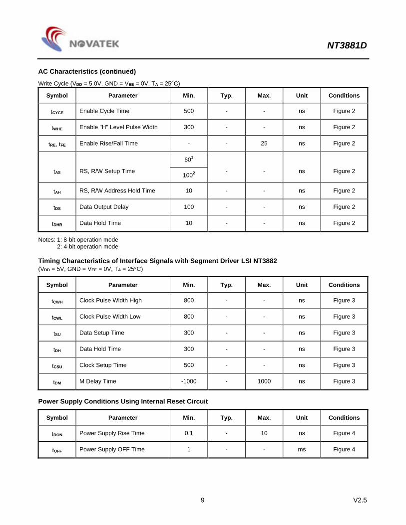
AC Characteristics (continued)
Write Cycle (VDD = 5.0V, GND = VEE = 0V, TA = 25°C)
Symbol Parameter Min. Typ. Max. Unit Conditions
tCYCE Enable Cycle Time 500 - - ns Figure 2
tWHE Enable "H" Level Pulse Width 300 - - ns Figure 2
tRE, tFE Enable Rise/Fall Time - - 25 ns Figure 2
601
tAS RS, R/W Setup Time 1002
- - ns Figure 2
tAH RS, R/W Address Hold Time 10 - - ns Figure 2
tDS Data Output Delay 100 - - ns Figure 2
tDHR Data Hold Time 10 - - ns Figure 2
Notes: 1: 8-bit operation mode 2: 4-bit operation mode Timing Characteristics of Interface Signals with Segment Driver LSI NT3882 (VDD = 5V, GND = VEE = 0V, TA = 25°C)
Symbol Parameter Min. Typ. Max. Unit Conditions
tCWH Clock Pulse Width High 800 - - ns Figure 3
tCWL Clock Pulse Width Low 800 - - ns Figure 3
tSU Data Setup Time 300 - - ns Figure 3
tDH Data Hold Time 300 - - ns Figure 3
tCSU Clock Setup Time 500 - - ns Figure 3
tDM M Delay Time -1000 - 1000 ns Figure 3
Power Supply Conditions Using Internal Reset Circuit
Symbol Parameter Min. Typ. Max. Unit Conditions
tRON Power Supply Rise Time 0.1 - 10 ns Figure 4
tOFF Power Supply OFF Time 1 - - ms Figure 4

NT3881D
10 V2.5
Timing Waveforms Read Operation
RS
R/W
E
DB0~DB7
VIH1
VIL1
VIH1
VIL1
VIH1
VIL1VIL1
VIH1
VIL1VIL1
VIH1VALD DATA
tDHR
tAH
tFE
tWEM
tRE
VIH1
VIL1
tAS tAH
tRD
tCYCE
Figure 1. Bus Read Operation Sequence
(Reading out data from NT3881D to MPU) Write Operation
RS
R/W
E
DB0 ~ DB7
VIH1
VIL1
VIH1
VIL1
VIL1
VIL1
VIH1
VIL1VIL1
VIH1VALD DATA
tDHW
tAH
tFE
tWEM
tRE
VIH1
VIL1
tAStAH
VIH1
VIL1
VIL1
tDS
tCYCE
Figure 2. Bus Write Operation Sequence
(Writing data from MPU to NT3881D)

NT3881D
11 V2.5
Timing Waveforms (continued) Interface Signals with Segment Driver LSI
0.9 VDD 0.9 VDD
0.1 VDD 0.9 VDD
tCWHtCWH
tCSU 0.9 VDD
0.1 VDD
tCWL
tDHtSU
0.9 VDD
0.1 VDD
0.1 VDD
CLK1
CLK2
D0.9 VDD
0.1 VDD
0.1 VDD
tDM
M
tCSU
Figure 3. Sending Data to Segment Driver LSI NT3882
Interface Signals with Segment Driver LSI (continued)
0.2V0.2V0.2V
4.5V
VDD tRON tOFFtOFF > 1ms0.1ms > tRON > 10ms
Figure 4. tOFF stipulates the time of power OFF for instantaneous power supply to or when power supply repeats ON and OFF. Note 1: The NT3881D has three clock options:
A. Internal Oscillator Operation (With Ceramic Filter)
CERAMICFILTER
OSC1 OSC2
C1 C2
Rf : 1MΩ ± 10% Rd : 3.3KΩ ± 5% C1 = C2 : 680pF ± 10%

NT3881D
12 V2.5
B. Internal Oscillator (With Rf Resistor)
OSC1 OSC2
Rf: 91kohm + 2%
Only Rf may be connected between OSC1 and OSC2. The wire connection Rf must be as short as possible.
C. External Clock Operation
OSC1 OSC2
PULSE INPUT
OSC1 and OSC2.
Note 2 : Input/Output Terminals: A. Input Terminal
Applicable Terminal : E (No Pull Up MOS)
PMOS
NMOS
VDD
Applicable Terminals: RS, R/W (with Pull Up MOS)
PULL UP MOS
NMOS
PMOS
VDD
PMOS
VDD

NT3881D
13 V2.5
B. Output Terminal Applicable Terminals: CL1, CL2, M, D
PMOS
NMOS
VDD
C. I/O Terminal Applicable Terminals: DB0 to DB7
PULL UP MOS
NMOS
PMOS
VDD
PMOS
VDD
VDD
ENABLE
PMOS
NMOS DATA
(OUTPUT CIRCUIT)(TRISTATE)

NT3881D
14 V2.5
Table 1. Correspondence between Character Codes and Character Patterns (NOVATEK Standard NT3881D-01)

NT3881D
15 V2.5
Table 2. Correspondence between Character Codes and Character Patterns (NOVATEK Standard NT3881D-02)

NT3881D
16 V2.5
Instruction Set
Instruction Code Function Executiontime (max)
RS RW DB7 DB6 DB5 DB4 DB3 DB2 DB1 DB0 (fOSC = 250KHz)
Display Clear
0
0
0
0
0
0
0
0
0
1
Clear entire display area, restore display from shift, and load address counter with DD RAM address 00H.
1.64ms
Display/ Cursor Home
0
0
0
0
0
0
0
0
1
*
Restore display from shift and load address counter with DD RAM address 00H.
1.64ms
Entry Mode Set
0
0
0
0
0
0
0
1
I/D
S
Specify direction of cursor movement and display shift mode. This operation takes place after each data transfer (read/write).
40µs
Display ON/OFF
0
0
0
0
0
0
1
D
C
B
Specify activation of display (D) cursor (C) and blinking of character at cursor position (B).
40µs
Display/ Cursor Shift
0 0 0 0 0 1 S/C R/L * * Shift display or move cursor. 40µs
Function Set
0
0
0
0
1
DL
N
F
*
*
Set interface data length (DL), number of display line (N), and character font (F).
40µs
RAM Address Set
0
0
0
1
ACG
Load the address counter with a CG RAM address. Subsequent data access is for CG RAM data.
40µs
DD RAM Address Set
0
0
1
ADD
Load the address counter with a DD RAM address. Subsequent data access is for DD RAM data.
40µs
Busy Flag/ Address Counter Read
0 1 BF AC
Read Busy Flag (BF) and contents of Address Counter (AC).
0µs
CG RAM/ DD RAM Data Write
1
0
Write data
Write data to CG RAM or DD RAM.
40µs
CG RAM/ DD RAM Data Read
1
1
Read data
Read data from CG RAM or DD RAM.
40µs
Note 1: Symbol "*" signifies an insignificant bit (disregard). Note 2: Correct input value for "N" is predetermined for each model.

NT3881D
17 V2.5
Instruction Set (continued)
Instruction Code Function Executiontime (max)
RS RW DB7 DB6 DB5 DB4 DB3 DB2 DB1 DB0 (fOSC = 250KHz)
I/D = 1 : Increment I/D = 0 : Decrement S = 1 : Display Shift On D = 1 : Display On C = 1 : Cursor Display On B = 1 : Cursor Blink On S/C = 1 : Shift Display S/C = 0 : Move Cursor R/L = 1 : Shift Right R/L = 0 : Shift Left DL = 1 : 8-Bit DL = 0 : 4-Bit N = 1 : Dual Line N = 0 : Signal Line F = 1 : 5x10 dots F = 0 : 5x8 dots BF = 1 : Internal Operation BF = 0 : Ready for Instruction
DD RAM : Display Data RAM CG RAM : Character Generator RAM ACG : Character Generator RAM Address ADD : Display Data RAM Address AC : Address Counter
Note 1: Symbol "*" signifies an insignificant bit (disregard). Note 2: Correct input value for "N" is predetermined for each model.

NT3881D
18 V2.5
Interface to LCD (1) Character Font and Number of Lines The NT3881D provides a 5 X 7 dot character font 1-line mode, a 5 X 10 dot character font 1-line mode and a 5 X 7 dot character font 2-line mode, as shown in the table below.
Three types of common signals are available as displayed in the table. The number of lines and the font type can be selected by the program.
Number of Lines Character Font Number of Common Signals Duty Factor
1 5 X 7 dots + Cursor (or 5x8 dots)
8 1/8
1 5 X 10 dots + Cursor 11 1/11
2 5 X 7 dots + Cursor (or 5x8 dots)
16 1/16
(2) Connection to LCD The following 4 LCD connection examples show the various combinations between characters and lines. NT3881D can directly drive the following combinations: (a) 5 X 8 Font - 8 character X 1 line (1/8 duty cycle, 1/4 bias)
NT3881D
COM1
COM8
SEG1
SEG40
LCD PANEL

NT3881D
19 V2.5
(b) 5 X 10 Font - 8 character X 1 line (1/11 duty cycle, 1/4 bias)
NT3881D
COM1
COM8
SEG1
SEG40
LCD PANEL
COM11
COM9
(c) 5 X 8 Font - 8 character X 2 lines (1/16 duty cycle, 1/5 bias)
NT3881D
COM1
COM8
SEG1
SEG40
LCD PANEL
COM16
COM9
NT3881D
20 V2.5
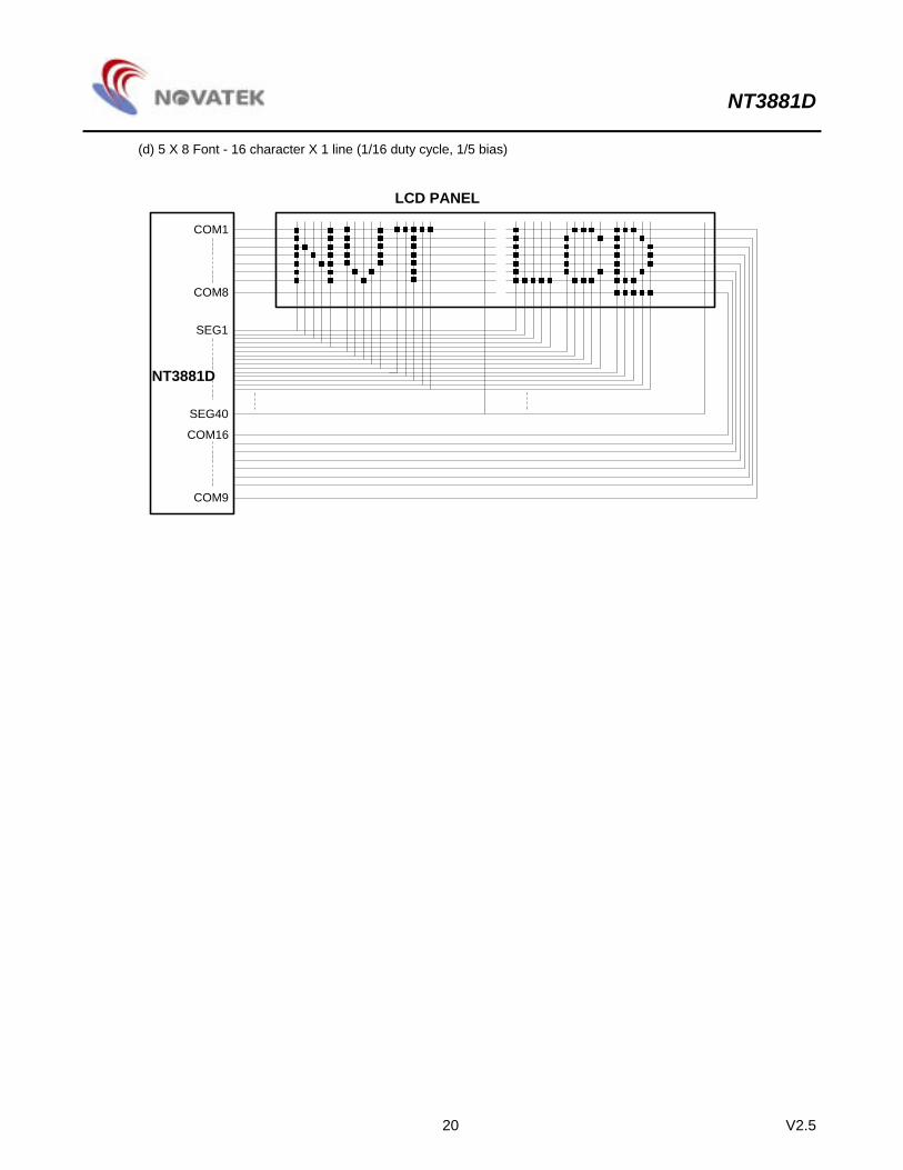
(d) 5 X 8 Font - 16 character X 1 line (1/16 duty cycle, 1/5 bias)
NT3881D
COM1
COM8
SEG1
SEG40
LCD PANEL
COM16
COM9

NT3881D
21 V2.5
(3) Bias Power Connection NT3881D provides 1/4 or 1/5 bias for various duty cycle applications. The power division voltage is described in the following table. The connection of NT3881D, power supply, and resistors are also shown as follows:
Power Division 1/8, 1/11 Duty Cycle - 1/4 Bias 1/16 Duty Cycle - 1/5 Bias
V1 VDD - 1/4 VLCD VDD - 1/5 VLCD
V2 VDD - 1/2 VLCD VDD - 2/5 VLCD
V3 VDD - 1/2 VLCD VDD - 3/5 VLCD
V4 VDD - 3/4 VLCD VDD - 4/5 VLCD
V5 VDD - VLCD VDD - VLCD
NT3881D
VDD
V1
V2
V3
V4
V5
VR
VEE
VDD
R
R
R
R
VLCD
VDD
V1
V2
V3
V4
V5
VR
VDD
R
R
R
R
R
VLCD
VEE
NT3881D
Note: The resistance value depends on the LCD panel size.

NT3881D
22 V2.5
(4) LCD Waveform A-type, 1/8 Duty Cycle, 1/4 Bias
400 CLOCKS
1 2 3 4 5 8 1 2
1 FRAME
VDD
V1
V2 (V3)
V4
V5
COM1
A-type, 1/11 Duty Cycle, 1/4 Bias
400 CLOCKS
1 2 3 4 5 11 1 2
1 FRAME
VDD
V1
V2 (V3)
V4
V5
COM1
A-type, 1/16 Duty Cycle, 1/5 Bias
200 CLOCKS
1 2 3 4 5 16 1 2
1 FRAME
VDD
V1
V2 (V3)
V4
V5
COM1

NT3881D
23 V2.5
B-type, 1/8 Duty Cycle, 1/4 Bias
COM1
VDD
V1
V2 (V3)
V4
V5
1 2 3 4 9
400 CLOCKS
1 Frame
11.9ms8400270K1secFrame 1 =××= 84.3Hz
11.9ms1Frequency Frame ==
5 6 7 8 16 21
B-type, 1/11 Duty Cycle, 1/4 Bias
COM1
VDD
V1
V2 (V3)
V4
V5
1 2 3 4 9
400 CLOCKS
1 Frame
16.3ms11400270K1sec1Frame =××= 61.4Hz
16.3ms1Frequency Frame ==
5 6 7 8 22 2110 11 12 21
B-type, 1/16 Duty Cycle, 1/5 Bias
COM1
VDD
V1
V2
V4
V5
1 2 3 4
200 CLOCKS
1 Frame
11.9ms16200270K1sec1Frame =××= 84.3Hz
11.9ms1Frequency Frame ==
5 32 2115 16 17 311413
V3

NT3881D
24 V2.5
Application Circuit (for reference only)
NT3881D
LCD PANEL
NT3882
C1 - C16 S1 - S40D
CL2
CL1
M
VDD
GND
V1
V2
V3
V4
V5
DL1
CL2
CL1
M
VDD
GND
V3 V4 V5
DR1
DL2
DR2
S1 - S40 S1 - S40
DR2
DL2
DR1
GND
VDD
M
CL1
CL2
DL1
R R R R R
VR
C C C C C
GND or othernegative voltage
SEL1
FCS
SEL2
FCS
SEL1
SEL2V2 V6V1 V3 V4 V5V2 V6V1
NT3882

NT3881D
25 V2.5
Bonding Diagram
1
2
3
4
5
6
7
8
9
10
11
12
13
14
15
16
17
18
19
20
21
22
23
24
25 26 27 28 29 30 31 32 81 34 35 36 37 38 39 40
41
42
43
44
45
46
47
48
49
50
51
52
53
54
55
56
57
58
59
60
61
62
63
64
656768697071727374757677787980
(0, 0)
NT3881DH
Y
X
3175 µm
3861 µm
66
33
* Substrate Connect to VDD or keep floating * Pad window area: 120 m X 110 m

NT3881D
26 V2.5
Bonding Dimensions Unit: µm
Pad No. Designation X Y Pad No. Designation X Y 1 SEG22 -1469 1743 41 DB2 1469 -1707 2 SEG21 -1469 1593 42 DB3 1469 -1557 3 SEG20 -1469 1443 43 DB4 1469 -1407 4 SEG19 -1469 1293 44 DB5 1469 -1257 5 SEG18 -1469 1143 45 DB6 1469 -1107 6 SEG17 -1469 993 46 DB7 1469 -957 7 SEG16 -1469 843 47 COM1 1469 -807 8 SEG15 -1469 693 48 COM2 1469 -657 9 SEG14 -1469 543 49 COM3 1469 -507
10 SEG13 -1469 393 50 COM4 1469 -357 11 SEG12 -1469 243 51 COM5 1469 -207 12 SEG11 -1469 93 52 COM6 1469 -57 13 SEG10 -1469 -57 53 COM7 1469 93 14 SEG9 -1469 -207 54 COM8 1469 243 15 SEG8 -1469 -357 55 COM9 1469 393 16 SEG7 -1469 -507 56 COM10 1469 543 17 SEG6 -1469 -657 57 COM11 1469 693 18 SEG5 -1469 -807 58 COM12 1469 843 19 SEG4 -1469 -957 59 COM13 1469 993 20 SEG3 -1469 -1107 60 COM14 1469 1143 21 SEG2 -1469 -1257 61 COM15 1469 1292 22 SEG1 -1469 -1407 62 COM16 1469 1443 23 GND -1469 -1557 63 SEG40 1469 1593 24 OSC1 -1469 -1707 64 SEG39 1469 1743 25 OSC2 -1183 -1862 65 SEG38 1125 1862 26 V1 -1033 -1862 66 SEG37 975 1862 27 V2 -883 -1862 67 SEG36 825 1862 28 V3 -733 -1862 68 SEG35 675 1862 29 V4 -583 -1862 69 SEG34 525 1862 30 V5 -433 -1862 70 SEG33 375 1862 31 CL1 -283 -1862 71 SEG32 225 1862 32 CL2 -133 -1862 72 SEG31 75 1862 33 VDDB 76 -1691 73 SEG30 -75 1862 34 M 268 -1862 74 SEG29 -225 1862 35 D 418 -1862 75 SEG28 -375 1862 36 RS 568 -1862 76 SEG27 -525 1862 37 R/W 719 -1862 77 SEG26 -675 1862 38 E 870 -1862 78 SEG25 -825 1862 39 DB0 1020 -1862 79 SEG24 -975 1862 40 DB1 1170 -1862 80 SEG23 -1125 1862 81 VDDA 76 -1816
NT3881D
27 V2.5
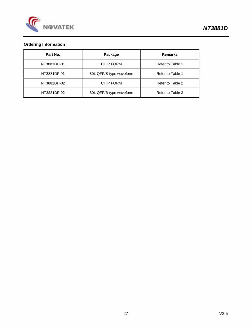
Ordering Information
Part No. Package Remarks
NT3881DH-01 CHIP FORM Refer to Table 1
NT3881DF-01 80L QFP/B-type waveform Refer to Table 1
NT3881DH-02 CHIP FORM Refer to Table 2
NT3881DF-02 80L QFP/B-type waveform Refer to Table 2

NT3881D
28 V2.5
Package Information
QFP 80L Outline Dimensions unit: inches/mm
A1A2 A
Seating Plane
1
24
b25 40
41
64
6580
E
e
GE
GD
See Detail F
Detail F
DHD
HE
D yL
GD ~ ~~
L1c
Symbol Dimensions in inches Dimensions in mm
A 0.130 Max. 3.30 Max.
A1 0.004 Min. 0.10 Min.
A2 0.112±0.005 2.85±0.13
b 0.014 +0.004 0.35 +0.10 -0.002 -0.05
c 0.006 +0.004 0.15 +0.10 -0.002 -0.05
D 0.551±0.005 14.00±0.13
E 0.787±0.005 20.00±0.13
e 0.031±0.006 0.80±0.15
GD 0.693 NOM. 17.60 NOM.
GE 0.929 NOM. 23.60 NOM.
HD 0.740±0.012 18.80±0.31
HE 0.976±0.012 24.79±0.31
L 0.047±0.008 1.19±0.20
L1 0.095±0.008 2.41±0.20
y 0.006 Max. 0.15 Max.
θ 0° ~ 12° 0° ~ 12°
Notes: 1. Dimensions D & E do not include resin fins. 2. Dimensions GD & GE are for PC Board surface mount pad pitch design reference only.

NT3881D
29 V2.5
Product Spec. Change Notice
NT3881 Specification Revision History
Version Content Date
2.5
Specification of operating voltage is added from 4.5V to 5.5V (Page 1, 7) Pin configuration drawing modified (Page 2, Added Pin 1 circle mark)
Dec.2002
2.4 B-type waveform modified(Page 23 , Document mistake corrected) Apr.2002
2.3 PAD 33 VDDB,PAD 81 VDDA modified( Page 5, 24) Nov.2001
2.2 Updated Page 16. Nov.2001
2.1 Updated all diagrams. Nov.1999
2.0 Modified Page1 -
1.0 NEW SPEC -