Standard Hardware API Design Guide - picmg.org · PDF fileM icroTCATM Standard Hardware API...
48
MicroTCA TM Standard Hardware API Design Guide Guideline for designing Hardware Access APIs for MTCA.4 Systems MTCA_DG.1 R1.0 January 9, 2017
Transcript of Standard Hardware API Design Guide - picmg.org · PDF fileM icroTCATM Standard Hardware API...

MicroTCATM
Standard Hardware API Design Guide Guideline for designing Hardware Access APIs for MTCA.4 Systems
MTCA_DG.1 R1.0 January 9, 2017


DISCLAIMER:
This design guide is not a specification. It contains additional detail information but does not
replace any applicable PICMG MTCA.4 specifications.
For complete guidelines on the design of MTCA.4 compliant boards and systems, refer also to the
full specification – do not use this design guide as the only reference for any design decisions.
© Copyright 2017, PCI Industrial Computer Manufacturers Group. The attention of adopters is
directed to the possibility that compliance with or adoption of PICMG® specifications may
require use of an invention covered by patent rights. PICMG® shall not be responsible for
identifying patents for which a license may be required by any PICMG® specification or for
conducting legal inquiries into the legal validity or scope of those patents that are brought to its
attention. PICMG® specifications are prospective and advisory only. Prospective users are
responsible for protecting themselves against liability for infringement of patents.
The information contained in this document is subject to change without notice. The material in
this document details a PICMG® specification in accordance with the license and notices set
forth on this page. This document does not represent a commitment to implement any portion of
this specification in any company's products.
WHILE THE INFORMATION IN THIS PUBLICATION IS BELIEVED TO BE ACCURATE,
PICMG® MAKES NO WARRANTY OF ANY KIND, EXPRESS OR IMPLIED, WITH
REGARD TO THIS MATERIAL INCLUDING, BUT NOT LIMITED TO, ANY WARRANTY
OF TITLE OR OWNERSHIP, IMPLIED WARRANTY OF MERCHANTABILITY OR
WARRANTY OF FITNESS FOR PARTICULAR PURPOSE OR USE.
In no event shall PICMG® be liable for errors contained herein or for indirect, incidental, special,
consequential, reliance or cover damages, including loss of profits, revenue, data or use, incurred
by any user or any third party. Compliance with this specification does not absolve manufacturers
of equipment from the requirements of safety and regulatory agencies (UL, CSA, FCC, IEC, etc.).
IMPORTANT NOTICE:
This document includes references to specifications, standards or other material not created by
PICMG. Such referenced materials will typically have been created by organizations that operate
under IPR policies with terms that vary widely, and under process controls with varying degrees
of strictness and efficacy. PICMG has not made any enquiry into the nature or effectiveness of
any such policies, processes or controls, and therefore ANY USE OF REFERENCED
MATERIALS IS ENTIRELY AT THE RISK OF THE USER. Users should therefore make such
investigations regarding referenced materials, and the organizations that have created them, as
they deem appropriate.
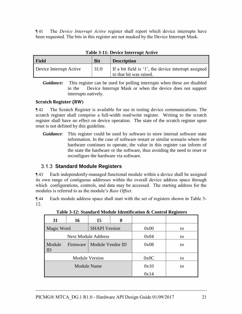
PICMG®, CompactPCI®, AdvancedTCA®, AdvancedTCA® 300,ATCA®, ATCA® 300,
CompactPCI® Express, COM Express®, SHB Express®, and the PICMG, CompactPCI,
AdvancedTCA, µTCA and ATCA logos are registered trademarks, and MicroTCA™, xTCA™,
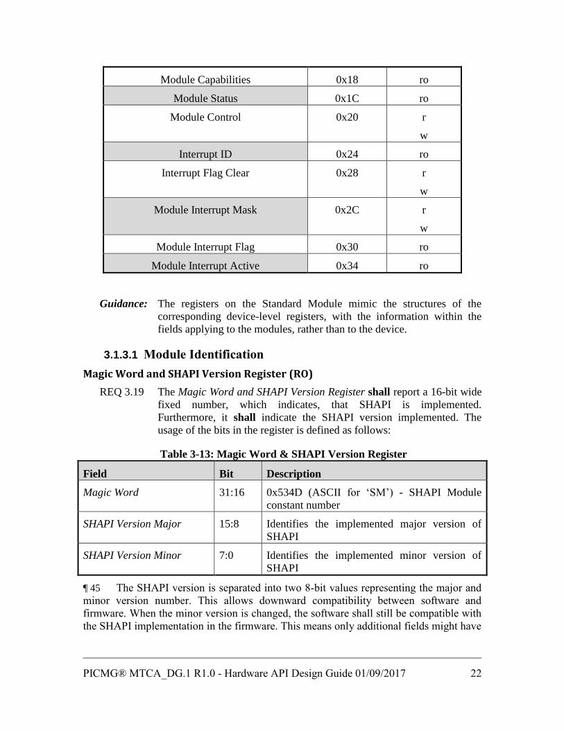
AdvancedMC™, IRTM™ and the IRTM logo are trademarks of the PCI Industrial Computer
Manufacturers Group. All other brand or product names may be trademarks or registered
trademarks of their respective holders.


PICMG® MTCA_DG.1 R1.0 - Hardware API Design Guide 01/09/2017 v
Contents
1 Preface ............................................................................................................................................... 1
1.1 About This Document ................................................................................................................................... 1
1.2 Intended Audience .......................................................................................................................................... 1
1.3 Special Word Usage ....................................................................................................................................... 1
1.4 Statements of Compliance .......................................................................................................................... 1
1.5 Correctness Disclaimer................................................................................................................................. 1
1.6 Name and Logo Usage .................................................................................................................................. 2
1.7 Intellectual Property ..................................................................................................................................... 2
1.8 Copyright Notice ............................................................................................................................................. 3
1.9 Acronyms and Abbreviations Used ......................................................................................................... 3
1.10 API Terminology ............................................................................................................................................. 4
2 Introduction ..................................................................................................................................... 6
2.1 Overview ............................................................................................................................................................. 6
2.2 Contributors ...................................................................................................................................................... 6
2.3 Nomenclature ................................................................................................................................................... 7
2.4 Background ....................................................................................................................................................... 8
Context and Rationale .................................................................................................................. 8
Guidance: Functional Requirements Summary ................................................................. 9
Technology and Operations Summary .................................................................................. 9
2.4.3.1 Address-Mapped I/O .......................................................................................................................... 9
2.4.3.2 Stream-Oriented I/O ......................................................................................................................... 10
2.4.3.3 Interrupts ............................................................................................................................................... 11
2.4.3.4 Hot Plugging ......................................................................................................................................... 11
3 Guidelines ...................................................................................................................................... 11
3.1 SHAPI Architecture ...................................................................................................................................... 11
Behavioral Model and Constraints ....................................................................................... 13
Standard Device Registers ....................................................................................................... 13
3.1.2.1 Device Identification ......................................................................................................................... 14
3.1.2.2 Device Management .......................................................................................................................... 18
Standard Module Registers ..................................................................................................... 21
3.1.3.1 Module Identification ....................................................................................................................... 22
3.1.3.2 Module Management ........................................................................................................................ 25
3.1.3.3 Module Interrupt Register Set ...................................................................................................... 27
PICMG® MTCA_DG.1 R1.0 - Hardware API Design Guide 01/09/2017 vi
4 Design Example ........................................................................................................................... 30
5 Standard Module Example ....................................................................................................... 31
6 Example of Interrupts ............................................................................................................... 35
7 Revision History .......................................................................................................................... 36
8 Table of Requirements .............................................................................................................. 37
PICMG® MTCA_DG.1 R1.0 - Hardware API Design Guide 01/09/2017 vii
Figures
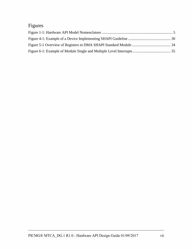
Figure 1-1: Hardware API Model Nomenclature ........................................................................... 5
Figure 4-1: Example of a Device Implementing SHAPI Guideline ............................................. 30
Figure 5-1 Overview of Registers in DMA SHAPI Standard Module ......................................... 34
Figure 6-1: Example of Module Single and Multiple Level Interrupts ........................................ 35
PICMG® MTCA_DG.1 R1.0 - Hardware API Design Guide 01/09/2017 viii
Tables
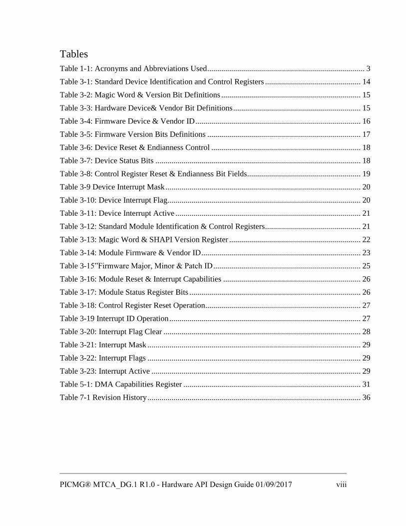
Table 1-1: Acronyms and Abbreviations Used ............................................................................... 3
Table 3-1: Standard Device Identification and Control Registers ................................................ 14
Table 3-2: Magic Word & Version Bit Definitions ...................................................................... 15
Table 3-3: Hardware Device& Vendor Bit Definitions ................................................................ 15
Table 3-4: Firmware Device & Vendor ID ................................................................................... 16
Table 3-5: Firmware Version Bits Definitions ............................................................................. 17
Table 3-6: Device Reset & Endianness Control ........................................................................... 18
Table 3-7: Device Status Bits ....................................................................................................... 18
Table 3-8: Control Register Reset & Endianness Bit Fields......................................................... 19
Table 3-9 Device Interrupt Mask .................................................................................................. 20
Table 3-10: Device Interrupt Flag................................................................................................. 20
Table 3-11: Device Interrupt Active ............................................................................................. 21
Table 3-12: Standard Module Identification & Control Registers ................................................ 21
Table 3-13: Magic Word & SHAPI Version Register .................................................................. 22
Table 3-14: Module Firmware & Vendor ID ................................................................................ 23
Table 3-15”Firmware Major, Minor & Patch ID .......................................................................... 25
Table 3-16: Module Reset & Interrupt Capabilities ..................................................................... 26
Table 3-17: Module Status Register Bits ...................................................................................... 26
Table 3-18: Control Register Reset Operation .............................................................................. 27
Table 3-19 Interrupt ID Operation ................................................................................................ 27
Table 3-20: Interrupt Flag Clear ................................................................................................... 28
Table 3-21: Interrupt Mask ........................................................................................................... 29
Table 3-22: Interrupt Flags ........................................................................................................... 29
Table 3-23: Interrupt Active ......................................................................................................... 29
Table 5-1: DMA Capabilities Register ......................................................................................... 31
Table 7-1 Revision History ........................................................................................................... 36

PICMG® MTCA_DG.1 R1.0 - Hardware API Design Guide 01/09/2017 ix
PICMG® MTCA_DG.1 R1.0 - Hardware API Design Guide 01/09/2017 1
1 Preface
1.1 About This Document
This guideline defines the functions and Application Programming Interfaces (APIs) for
the general-use hardware module developed for the MTCA.4 effort within PICMG. It is
applicable to systems developed in conjunction with the standards released as part of that
effort, and more generally to systems developed for instrumentation and machine control
applications.
This guideline defines a standard operating model and Application Programming
Interface (API) for board hardware and code development to facilitate module re-use and
portability. It is recommended, but not required, that applications developed for use with
MTCA.4 systems make use of these guidelines to the greatest reasonable extent.
This guideline applies specifically to devices with complex configuration, management,
and data access requirements that fall outside the paradigm of a simple stream data access
mechanism. It is not intended or appropriate for use with simple data streaming devices.
This design guide is not a specification. It contains additional detail information, but
does not replace any applicable PICMG MTCA.4 specifications.
For complete guidelines on the design of MTCA.4 compliant boards and systems, refer
also to the full specification; do not use this design guide as the only reference for any
design decisions.
1.2 Intended Audience
This design guide is intended for hardware engineers, software engineers, and
programmers designing boards and software for use with MTCA.4 systems.
1.3 Special Word Usage
Even though this is a Guideline and not a Specification, it is necessary to make
recommendations that can be considered mandatory if the user wants to maintain
maximum interoperability with other users. Therefore the standard Requirements
protocol has been used to flag those situations with “shall” and “should” statements.
1.4 Statements of Compliance
Compliance with the Guideline is completely optional with the warning stated above.
1.5 Correctness Disclaimer
The code examples given in this document are believed to be correct but no guarantee is
given. In most cases the examples come from designs that have been built and tested.
PICMG® MTCA_DG.1 R1.0 - Hardware API Design Guide 01/09/2017 2
1.6 Name and Logo Usage
The PCI Industrial Computer Manufacturers Group’s policies regarding the use of its
logos and trademarks are as follows:
Permission to use the PICMG organization logo is automatically granted to designated
members only as stipulated on the most recent Membership Privileges document
(available at www.picmg.org) during the period of time for which their membership dues
are paid. Nonmembers must not use the PICMG organization logo.
The PICMG organization logo must be printed in black or color as shown in the files
available for download from the member’s side of the Web site. Logos with or without
the “Open Modular Computing Specifications” banner can be used. Nothing may be
added or deleted from the PICMG logo.
The PICMG® name and logo are registered trademarks of The PICMG®. Registered
trademarks must be followed by the ® symbol, and the following statement must appear
in all published literature and advertising material in which the logo appears:
PICMG and the PICMG logo are registered trademarks of the PCI Industrial Computer
Manufacturers Group.
1.7 Intellectual Property
The Consortium draws attention to the fact that implementing recommendations made in
this document could involve the use of one or more patent claims (“IPR”). The
Consortium takes no position concerning the evidence, validity, or scope of this IPR.
Attention is also drawn to the possibility that some of the elements of this specification
could be the subject of unidentified IPR. The Consortium is not responsible for
identifying any or all such IPR.
No representation is made as to the availability of any license rights for use of any IPR
that might be required to implement the recommendations of this Guide. This document
conforms to the Specification Development and doASCIIes not contain any known
intellectual property that is not available for licensing under Reasonable and
Nondiscriminatory terms. In the course of Membership Review the following disclosures
were made:
Necessary Claims (referring to mandatory or recommended features):

PICMG® MTCA_DG.1 R1.0 - Hardware API Design Guide 01/09/2017 3
No disclosures in this category were made during Member Review
Unnecessary Claims (referring to optional features or non-normative elements):
No disclosures in this category were made during Member Review
Third Party Disclosures (Note that third party IPR submissions do not contain any claim
of willingness to license the IPR.):
No disclosures in this category were made during Member Review
THIS DOCUMENT IS BEING OFFERED WITHOUT ANY WARRANTY
WHATSOEVER, AND IN PARTICULAR, ANY WARRANTY OF
NONINFRINGEMENT IS EXPRESSLY DISCLAIMED. ANY USE OF THIS
DOCUMENT SHALL BE MADE ENTIRELY AT THE IMPLEMENTER’S OWN
RISK, AND NEITHER THE CONSORTIUM, NOR ANY OF ITS MEMBERS OR
SUBMITTERS, SHALL HAVE ANY LIABILITY WHATSOEVER TO ANY
IMPLEMENTER OR THIRD PARTY FOR ANY DAMAGES OF ANY NATURE
WHATSOEVER, DIRECTLY OR INDIRECTLY, ARISING FROM THE USE OF
THIS DOCUMENT.
1.8 Copyright Notice
Copyright © 2016, PICMG. All rights reserved. All text, pictures, and graphics are
protected by copyrights. No copying is permitted without written permission from
PICMG.
PICMG has made every attempt to ensure that the information in this document is
accurate, yet the information contained within is supplied “as-is”.
Trademarks
PCI Express is a registered trademark of Peripheral Component Interconnect Special
Interest Group (PCI-SIG). All product names and logos are property of their owners.
1.9 Acronyms and Abbreviations Used
Table 1-1: Acronyms and Abbreviations Used
Word(s) Definition
API Application Programming Interface
ASCII American Standard Code for Information Interchange
ATCA Advanced Telecommunication Computing Architecture
BAR Base Address Registers
LSB Least Significant Bit
MTCA MicroTCA
PICMG® MTCA_DG.1 R1.0 - Hardware API Design Guide 01/09/2017 4
1.10 API Terminology
For purposes of describing the Standard Hardware API and its environment the following
terminology is applicable and is illustrated in Figure 1; highlighted elements are the
subject of this guideline:
Channel The logical communication path between a hardware device
management/data interface and the software accessing that device.
Includes both electronic and software components.
Device A hardware component which interacts with software through a
communication path; may refer either to a Physical Device or to a
Logical Device, depending on context
Logical Device The API through which a Physical Device is accessed
Module Independently-managed functional component within a device
Physical Device A hardware board/board subsystem
Register A single location within an addressable I/O space

PICMG® MTCA_DG.1 R1.0 - Hardware API Design Guide 01/09/2017 5
PHY
Protocol
Encoder/Decoder
Protocol Formatter/
Parser
FPGA
Register Set or
Application
Logical
ADC
Formatter
/Parser
Encoder/
Decoder
Physical
ADC Ph
ys
ica
l De
vic
e
Lo
gic
al D
ev
ice
Pro
toc
ol
Ch
an
ne
l
PHY
Protocol
Encoder/Decoder
Protocol Formatter/
Parser
Ch
an
ne
lP
roto
co
l
Standard
Addressable Device
Model
FPGA API Model
Logical ADC Model
Application
De
vic
e M
od
el S
tac
k
PCIe, Ethernet,
SRIO, USB,
RS232, custom
bus
Message-
based or
bus-based
Mapped into
Addressable
Space
Parameterized
API &
State-Machine
Sta
nd
ard
AP
Is
FP
GA
Lo
gic
So
ftwa
re
Standard
Communication
Model
Hardware API
Hardware
PHY
Pa
ss-T
hro
ug
h L
ay
er
FPGA
Virtualization
Figure 1-1: Hardware API Model Nomenclature

PICMG® MTCA_DG.1 R1.0 - Hardware API Design Guide 01/09/2017 6
2 Introduction
2.1 Overview
¶ 1 The Advanced Telecommunication Computing Architecture (ATCA)
specification and related standards maintained by the PCI Industrial Computer
Manufacturers Group (PICMG) define an infrastructure for development of distributed
data processing systems for the telecommunications industry. At the urging of the
experimental physics community a set of committees were formed under the auspices of
PICMG to extend the ATCA family of standards for use in embedded instrumentation
and machine control applications, with particular emphasis on scientific applications.
These committees, known collectively as the MTCA.4 committees, were chartered to
adapt and/or extend the existing ATCA family specifications to accommodate sensor and
control I/O, including: support for analog signals; timing, synchronization, and interlock
mechanisms required for instrumentation and control operations; and low latency data
distribution protocols to support time-critical data processing and control constraints.
As part of the standardization effort the committees also defined common development
architectures to encourage hardware and software component interoperability and
portability among the various scientific centers. To that end, guidelines for various
aspects of hardware and software development of MTCA.4 systems were developed and
published.
This guideline defines the function and usage for a Standard Hardware API especially
for, but not limited to, use in MTCA.4 applications.
2.2 Contributors
The following companies and institutions contributed to the creation of this
document:
DESY/XFEL Germany
Institute of High Energy Physics (IHEP) PR China
Pentair Schroff Germany/USA
ITER France
IPFN Portugal
SLAC National Accelerator Laboratory USA
Triple Ring Technologies USA
VadaTech USA

PICMG® MTCA_DG.1 R1.0 - Hardware API Design Guide 01/09/2017 7
2.3 Nomenclature
¶ 1 Recommendations are designated within this document by the words shall, will,
should, is, and are. These terms are interchangeable and usage is driven entirely by
context and stylistic considerations.
¶ 2 Although this is a guideline, rather than a standard, its intent is to define
mechanisms and practices that facilitate interoperability of hardware and software
modules across different projects and facilities. As such, it is useful to provide language
that allows a discussion among implementers about the degree to which their applications
do or do not conform to the recommendations presented here, and therefore the degree to
which they can expect that goal of interoperability to be achieved. To that end, four
levels of recommendation may be identified:
• Mandatory: These recommendations must be implemented to be fully conformant
with this guideline.
• Required: These recommendations must be implemented to be fully
conformant with this guideline, but may be excluded from a particular
implementation provided the release notes for the implementation specifically
identify them as areas of non-conformance. An implementation with exclusions
may be considered “conditionally conformant”.
• Desired: These recommendations comprise design goals, performance
targets, and “nice to haves” that are desirable but not necessary for full
conformance with this guideline. Application developers should not depend on
availability of these items on all implementations.
• Guidance: These recommendations are provided for guidance and clarification to
the designer regarding the intent of other specific recommendations, expected
guideline usage, external interfaces and constraints, and preferred or potential
design approaches, technologies, and practices. These items should be taken into
account during design and deviations may be noted within the standard design
documentation, but they are not binding for design.
Required, Desired, and Guidance recommendations must be specifically
designated as such within the text of the specification. Any recommendation
without such a designation is presumed to be Mandatory.
PICMG® MTCA_DG.1 R1.0 - Hardware API Design Guide 01/09/2017 8
2.4 Background
Context and Rationale
¶ 3 The Standard Hardware API (SHAPI) defined in this guideline is intended to
apply to applications developed in conjunction with the MTCA.4 family of standards
from PICMG. These applications typically involve large networks of distributed
computing elements, sensors, actuators, and signal generators forming integrated control
and data acquisition/analysis systems. Although such systems will often make use of
large general-purpose computing platforms for system monitoring/control and offline
analysis, a large fraction of hardware and software components in such systems operate
within embedded environments, remote from the high-level control/analysis systems and
with soft and hard real-time requirements.
¶ 4 Further, the operating environment for such systems is anticipated to be dynamic
in terms of both hardware and software configuration as experiments evolve, and to
involve a high degree of sharing, both of expertise and of actual hardware and software
modules, among the various laboratories participating in the work. Both the dynamic
nature of the environment and the degree of sharing between facilities leads to a strong
desire for a hardware and software development infrastructure that facilitates rapid
prototyping of new components, efficient code development and validation, and device
and code portability. That desire has been formalized by the PICMG MTCA.4 Software
and Protocols committee as a set of guidelines for creating standard I/O interfaces,
communication protocols, and other commonly used functional blocks and APIs. This
standard defines the hardware API model which supports standardized hardware access
functions.
¶ 5 The purpose of the SHAPI guideline is to provide a standardized and portable
way for software applications to interact with physical hardware devices.
¶ 6 The SHAPI defines a standardized Application Programming Interface (API)
suitable for interacting with most types of hardware devices. The SHAPI defines the
logical structure for device access; it does not define or restrict the physical channels
through which device communications occur and does not address the mechanisms by
which software accesses such channels.
Guidance: This guideline defines a structural and methodological approach to device
access for purposes of increasing application robustness and portability
and to facilitate rapid application development. In an effort to assist
developers and encourage adoption of this guideline various code
libraries and example applications will be developed and made publicly
available as part of the guideline development project; and it is assumed

PICMG® MTCA_DG.1 R1.0 - Hardware API Design Guide 01/09/2017 9
that further libraries and examples will be made available by the
developer community as the guideline is adopted. However, although
this guideline itself will be maintained by PICMG under version control,
the various SHAPI code sets do not constitute a tool-set per se in the
sense of a single integrated, managed, maintained, and version-
controlled package. Rather, the SHAPI should be considered a logical
framework for hardware and software development, and the associated
code sets should be considered open-source design resources available to
developers for integration into, or as templates for creating, their own
projects.
Guidance: Functional Requirements Summary
¶ 7 Figure 1-1 illustrates a ‘typical’ hardware device and its relationship to a software
application. As shown, it comprises:
• A physical device, in this case an analog-to-digital converter, which performs
some system function
• A logical device interface at the hardware level through which the physical device
may be configured/monitored and through which device-related data may be
moved.
• A channel through which device-related information is transmitted; the channel
may comprise both physical and logical (e.g. protocol) components.
• A logical device model/stack by which software connects to the channel; the
device model/stack exposes a logical device interface at the software level
through which the application interacts with the device.
• Application software which utilizes the device to perform some system function
¶ 8 This guideline applies to the logical device interfaces at both the hardware and the
software levels (highlighted in the figure). The overall requirement for the logical device
API is to:
• Define a standardized access paradigm that is independent of the physical and
logical channel through which access flows
• Define a common method for device identification and top-level device control
• Define a common method for customization of the API for use with specific
devices
Technology and Operations Summary
¶ 9 The following sections describe the various types of device functions, access
mechanisms, and operating paradigms a Standard Hardware API must accommodate.
2.4.3.1 Address-Mapped I/O
¶ 10 At the fundamental hardware level internal and external software-accessible
hardware components connected to a processor core are almost always mapped in some
fashion into the processor’s address space, and software access to these components
operates by reading to or writing from the appropriate addressable elements. Address-

PICMG® MTCA_DG.1 R1.0 - Hardware API Design Guide 01/09/2017 10
Mapped I/O is the general term used to describe way a processor accesses these
components – the processor reads (I) data from/writes (O) data to the hardware
component, or “device”, by reading from or writing to a location in its addressable space.
¶ 11 Aside from its close alignment with the physical implementation of processor-
connected devices, this I/O model is also a generally useful paradigm for access to any
device, physical or logical, which can be modeled as having some store of static data that
may be changed from time to time.
¶ 12 An Address-Mapped access model is well-suited to modeling the structure of data
held within a device, with each datum accessible at its allotted place within the structure.
2.4.3.2 Stream-Oriented I/O
¶ 13 A stream is a model for an ordered, sequential flow of data rather than for data
statically arranged within a fixed structure. A stream can model a temporal flow (eg. the
samples reported by a data acquisition module) or it can model a geometric flow (eg. the
sequence of bytes within a file). In practice all stream APIs are temporal in nature
because the software accesses are sequential in time, but the crucial aspect of a stream
interface is ordering not timing; time is merely the by-product of sequence in any real-
world system. In a stream API the order of data passed into the interface is maintained,
such that when it appears for output at some other stream interface – say at the receiving
end of a communication channel or when it is read back from a disk – the original
ordering is intact.
¶ 14 Some streams are identified as “addressable” or as supporting “random access” –
that is, they provide a mechanism for altering the ordering of data within the stream by
moving the “location” at which the next element submitted through the interface will
appear. This functionality is restricted to devices modeling geometric sequences, like
disk drives, since a temporal sequence is ephemeral; you cannot rearrange the past. It
might appear that an addressable stream model for device access is no different than an
address-mapped model, but even an addressable stream enforces ordering: changing the
stream “address” merely moves the starting point within the sequence for subsequent data
transfers; the transfers themselves still proceed in sequential order from that starting
point.
¶ 15 For practical implementation purposes, a “stream” may be modeled as a
sequential access through a single device access port. Hence, it is easily mapped into an
addressable I/O space by assigning a specific address through which the stream data is
accessed.

PICMG® MTCA_DG.1 R1.0 - Hardware API Design Guide 01/09/2017 11
2.4.3.3 Interrupts
¶ 16 Interrupts and interrupt handling are generally coupled to the platform hardware
environment. A standardized model is described in this guideline which should be
compatible with different devices and cope with multiple interrupt sources or multiple
interrupts generated by a single module.
¶ 17 This model allows one to identify and manage the Module(s) responsible for
generating interrupts and their priority. Modules can have multiple interrupt sources, and
each one can be individually enabled. Acknowledge and reset of Interrupt flags are
handled at a Module level.
¶ 18 A single Module can also generate multiple device level interrupts. In such case,
the registers responsible for identifying and enabling sources are not used.
2.4.3.4 Hot Plugging
¶ 19 Hot plugging guidelines for MTCA.4 applications are not covered in this
document. Standard operating and usage models and the related API are defined in the
PICMIG document PCI Express Hot Plug Design Guide. That guideline defines a
standard usage model for all devices and software components that support hot plug
capabilities. However a separate MTCA.4 Hot Plug procedure Guideline is also under
construction.
3 Guidelines
3.1 SHAPI Architecture
REQ 3.1 The fundamental paradigm for device access defined by the SHAPI
shall be an addressable I/O space through which various device
functions may be managed. That paradigm applies at both the hardware
and software levels identified in Figure 1-1.
¶ 20 The fundamental data access element within the SHAPI is a register, which
represents an element accessible through a single I/O address.
Guidance: The use of the term “register” is not intended to imply any particular
hardware implementation. It merely designates a logical element at a
single address in the addressable space. Data accessed through a logical
“register” may be held in a physical register or in some dynamic
PICMG® MTCA_DG.1 R1.0 - Hardware API Design Guide 01/09/2017 12
memory element, or it may be generated on-the-fly during a read and/or
invoke some logical process, rather than being stored, during a write.
REQ 3.2 All Registers shall be 32-bits wide and presented at the software API in
native processor byte-order.
Guidance: This basic access paradigm is independent of the physical channel
through which accesses are routed. If the physical access channel
includes a serial communication link, the packetization on the link
should implement access to registers in the logical address space.
Guidance: For hardware that is designed in accordance with this guideline and
exposes the standard SHAPI at its logical interface, the logical software
API may be simply a pass-through of the hardware implementation.
¶ 21 For hardware that was not designed in accordance with this guideline, the logical
software API shall provide a mapping between the SHAPI at the application interface and
the underlying hardware device implementation, such that the application interface to the
device conforms to this guideline.
Guidance: To the extent that hardware devices are designed in accordance with this
guideline and export the SHAPI, the device model stack shown in Figure
1 will be a common element applicable to all devices, minimizing the
effort involved in connecting to new devices as they are added to the
system. Adaptation to non-SHAPI devices at the software logical device
level will allow applications to interact with those devices as if they
were SHAPI devices; this requires some software effort to do the
adaptation, but means that application software may be developed
independently of the details of particular hardware devices.
REQ 3.3 Devices shall export a logical access API which comprises an
addressable space through which registers may be accessed.

PICMG® MTCA_DG.1 R1.0 - Hardware API Design Guide 01/09/2017 13
Behavioral Model and Constraints
REQ 3.4 Devices shall map all configuration, control, and data flow functions
into the addressable register API.
REQ 3.5 Within hardware devices, register sets that represent monolithic data
elements wider than 32-bits at successive addresses shall be accessed in
little-endian word-order.
REQ 3.6 Desired: Devices shall minimize the use of stream-oriented “command
sequences” and instead, implement controls through arrays of static
configuration and control registers.
Desired: Information written into a register that persists in some form (eg. stored
data or a hardware configuration) should be readable through the same
register; there should be no “write-only” configurations and/or data.
Guidance: If a particular piece of hardware does not provide a capability for
readback, the logical device API adaptation at the software level should
mirror the information and provide the readback capability.
Standard Device Registers
¶ 22 At a minimum, SHAPI devices shall expose a standard device register set as
shown in Table 3-1. The following sections defined the contents of the standard registers.
Guidance: If a device supports multiple Base Address Registers (BARs) and
implements SHAPI, it is not necessary that all BARs conform to SHAPI,
or that the ones which confrom to SHAPI are consecutive. However, the
first BAR that implements the SHAPI guideline shall start with the
Standard Device register set. Other BARs that implement SHAPI start
with a Standard Module register set as described in section 3.1.3.

PICMG® MTCA_DG.1 R1.0 - Hardware API Design Guide 01/09/2017 14
Table 3-1: Standard Device Identification and Control Registers
31 16 15 0
Magic Word SHAPI Version 0x00 ro
First Module Address 0x04 ro
Hardware ID Hardware Vendor ID 0x08 ro
Device Firmware ID Device Vendor ID 0x0C ro
Firmware Version 0x10 ro
Firmware Timestamp 0x14 ro
Firmware Name
0x18 ro
0x1C ro
0x20 ro
Device Capabilities 0x24 ro
Device Status 0x28 ro
Device Control 0x2C rw
Device Interrupt Mask 0x30 rw
Device Interrupt Flag 0x34 ro
Device Interrupt Active 0x38 ro
Scratch Register 0x3C rw
3.1.2.1 Device Identification
¶ 23 The following registers allow identification of the device and also provide the
information concerning its version:
3.1.2.1.1 Magic Word and SHAPI Version 1.0

PICMG® MTCA_DG.1 R1.0 - Hardware API Design Guide 01/09/2017 15
REQ 3.7 The Magic Word and SHAPI Version Register shall report a 16-bit wide
fixed number, which indicates that SHAPI is implemented. Furthermore,
it shall indicate the SHAPI version implemented. The bits in the register
are defined as follows:
Table 3-2: Magic Word & Version Bit Definitions
¶ 24 The SHAPI version is separated into two 8-bit values representing the major and
minor version number. This document describes SHAPI version 1.0, therefore a device
following this guideline shall have the value of 1 in bits 15:8 and 0 in bits 7:0 of the
Magic Word and SHAPI Version register.
3.1.2.1.2 First Module Address (RO)
REQ 3.8 The First Module Address shall report the absolute address of the first
module in the firmware. Each module register address space starts with a
standard set as specified in 3.1.3. A value of ‘0’ shall be reserved to
designate that no modules are implemented.
Guidance: If a device supports multiple BAR, a value of ‘0’ indicates that there are
no modules implemented in the current BAR. SHAPI Modules can be
implemented in other BARs, in which case the BAR starts with a
Standard Module register set as described in section 3.1.3.
3.1.2.1.3 Hardware ID and Hardware Vendor ID (RO)
REQ 3.9 The Hardware ID and Hardware Vendor ID Register shall report a
unique device identifier for each unique device vendor. The register
shall comprise two 16-bit fields, as follows:
Table 3-3: Hardware Device& Vendor Bit Definitions
Field Bit Description
Hardware ID 31:16 Identifies the hardware device
Hardware Vendor ID 15:0 Identifies the hardware device vendor
Field Bit Description
Magic Word 31:16 0x5348 (ASCII for ‘SH’) - SHAPI Hardware
constant number
SHAPI VersionMajor 15:8 Identifies the implemented major version of
SHAPI
SHAPI Version Minor 7:0 Identifies the implemented minor version of
SHAPI
PICMG® MTCA_DG.1 R1.0 - Hardware API Design Guide 01/09/2017 16
REQ 3.10 The Hardware ID shall be assigned by the vendor or, in the case of a
“standard” API, by PICMIG.
REQ 3.11 The Hardware Vendor ID shall be unique to each board vendor and shall
identify the entity responsible for the board design. The Hardware
Vendor ID shall be assigned by PICMIG.
REQ 3.12 A Hardware Vendor ID value of 0 shall be reserved to designate devices
that implement an agreed-upon “standard” API that is not unique to a
particular vendor.
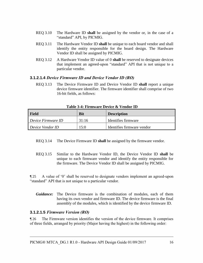
3.1.2.1.4 Device Firmware ID and Device Vendor ID (RO)
REQ 3.13 The Device Firmware ID and Device Vendor ID shall report a unique
device firmware identifier. The firmware identifier shall comprise of two
16-bit fields, as follows:
Table 3-4: Firmware Device & Vendor ID
Field Bit Description
Device Firmware ID 31:16 Identifies firmware
Device Vendor ID 15:0 Identifies firmware vendor
REQ 3.14 The Device Firmware ID shall be assigned by the firmware vendor.
REQ 3.15 Similar to the Hardware Vendor ID, the Device Vendor ID shall be
unique to each firmware vendor and identify the entity responsible for
the firmware. The Device Vendor ID shall be assigned by PICMIG.
¶ 25 A value of ‘0’ shall be reserved to designate vendors implement an agreed-upon
“standard” API that is not unique to a particular vendor.
Guidance: The Device firmware is the combination of modules, each of them
having its own vendor and firmware ID. The device firmware is the final
assembly of the modules, which is identified by the device firmware ID.
3.1.2.1.5 Firmware Version (RO)
¶ 26 The Firmware version identifies the version of the device firmware. It comprises
of three fields, arranged by priority (Major having the highest) in the following order:

PICMG® MTCA_DG.1 R1.0 - Hardware API Design Guide 01/09/2017 17
Table 3-5: Firmware Version Bits Definitions
Field Bit Description
Firmware Version Major 31:24 Identifies the Major version of the Firmware
Firmware Version Minor 23:16 Identifies the Minor version of the Firmware
Firmware Version Patch 15:0 Identifies the Patch version of the Firmware
REQ 3.16 When a version field is increased, the corresponding lower priority fields
shall be reset.
Guidance: Similar to the SHAPI version, the firmware version fields identify
downward compatibility between software and firmware. An increase in
a version field reflects the following:
• Major Value: software compatibility is no longer assured;
• Minor Value: changes in the firmware and device level registers which
do not interfere with available software;
• Patch Value: internal firmware changes with no effect to external
interfaces.
3.1.2.1.6 Firmware Timestamp (RO)
REQ 3.17 The Firmware Timestamp shall report the UNIX timestamp of the
firmware version currently running on the device. The value shall be
reported in unsigned 32 bit integer format.
Guidance: The time can correspond to the compilation or release time of the
firmware.
3.1.2.1.7 Firmware Name (RO)
¶ 27 The Firmware Name shall report up to 12 ASCII characters, used to name the
firmware currently running in the device. Unused characters should be placed in the least
significant bit fields and filled with null bytes.
Guidance: The information on this register may be used by the device driver in
order to name the driver device file. The usage of this register may not
strictly conform to the “firmware name” designator when the values in
the Firmware Device and Vendor ID are sufficient to properly identify
the device.
PICMG® MTCA_DG.1 R1.0 - Hardware API Design Guide 01/09/2017 18
3.1.2.2 Device Management
¶ 28 The following registers allow users to read and change the current state of the
device, read its capabilities and enable or disable certain features.
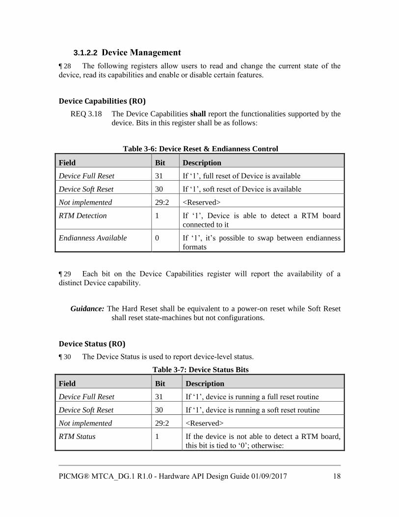
Device Capabilities (RO)
REQ 3.18 The Device Capabilities shall report the functionalities supported by the
device. Bits in this register shall be as follows:
Table 3-6: Device Reset & Endianness Control
Field Bit Description
Device Full Reset 31 If ‘1’, full reset of Device is available
Device Soft Reset 30 If ‘1’, soft reset of Device is available
Not implemented 29:2 <Reserved>
RTM Detection 1 If ‘1’, Device is able to detect a RTM board
connected to it
Endianness Available 0 If ‘1’, it’s possible to swap between endianness
formats
¶ 29 Each bit on the Device Capabilities register will report the availability of a
distinct Device capability.
Guidance: The Hard Reset shall be equivalent to a power-on reset while Soft Reset
shall reset state-machines but not configurations.
Device Status (RO)
¶ 30 The Device Status is used to report device-level status.
Table 3-7: Device Status Bits
Field Bit Description
Device Full Reset 31 If ‘1’, device is running a full reset routine
Device Soft Reset 30 If ‘1’, device is running a soft reset routine
Not implemented 29:2 <Reserved>
RTM Status 1 If the device is not able to detect a RTM board,
this bit is tied to ‘0’; otherwise:
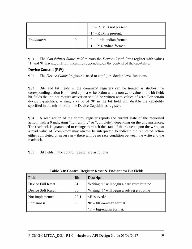
PICMG® MTCA_DG.1 R1.0 - Hardware API Design Guide 01/09/2017 19
‘0’ – RTM is not present
‘1’ – RTM is present.
Endianness 0 ‘0’ – little-endian format
‘1’ – big-endian format.
¶ 31 The Capabilities Status field mirrors the Device Capabilities register with values
‘1’ and ‘0’ having different meanings depending on the context of the capability.
Device Control (RW)
¶ 32 The Device Control register is used to configure device-level functions.
¶ 33 Bits and bit fields in the command registers can be treated as strobes; the
corresponding action is initiated upon a write action with a non-zero value in the bit field;
bit fields that do not require activation should be written with values of zero. For certain
device capabilities, writing a value of ‘0’ in the bit field will disable the capability
specified in the mirror bit on the Device Capabilities register.
¶ 34 A read action of the control register reports the current state of the requested
action, with a 0 indicating “not running” or “complete”, depending on the circumstances.
The readback is guaranteed to change to match the state of the request upon the write, so
a read value of “complete” may always be interpreted to indicate the requested action
either completed or never ran – there will be no race condition between the write and the
readback.
¶ 35 Bit fields in the control register are as follows:
Table 3-8: Control Register Reset & Endianness Bit Fields
Field Bit Description
Device Full Reset 31 Writing ‘1’ will begin a hard reset routine
Device Soft Reset 30 Writing ‘1’ will begin a soft reset routine
Not implemented 29:1 <Reserved>
Endianness 0 ‘0’ – little-endian format.
‘1’ – big-endian format.

PICMG® MTCA_DG.1 R1.0 - Hardware API Design Guide 01/09/2017 20
3.1.2.2.1 Device Interrupt Register Set
¶ 36 The following registers allow users to configure the interrupts generated by the
device as well as identifying the source module.
Device Interrupt Mask (RW)
¶ 37 The Device Interrupt Mask register configures which device interrupts are
enabled.
Table 3-9 Device Interrupt Mask
Field Bit Description
Device Interrupt Mask 31:0 A bit field of ‘1’ enables device interrupts
assigned to that bit.
¶ 38 A value of ‘1’ in a bit field of the Device Interrupt Mask enables interrupt
generation at the CPU level for interrupt assigned to that specific bit.
¶ 39 Interrupt sources are identified via the Module Interrupt ID register, described in
section 3.1.3.2. Priority of Interrupts is asserted by bit position, with LSBs having higher
priority.
Guidance: By reading all the Interrupt ID registers available in the hardware, the
software can build up a look-up table which relates each bit in the
Device Interrupt Mask, Flags and Active register with the correspondent
Module.
Device Interrupt Flag (RO)
¶ 40 The Device Interrupt Flag register shall report which device interrupts have been
requested. The bits in this register are masked by the Device Interrupt Mask.
Table 3-10: Device Interrupt Flag
Field Bit Description
Device Interrupt Flag 31:0 If a bit field is ‘1’, the device interrupt assigned
to that bit was raised.
Device Interrupt Active (RO)
PICMG® MTCA_DG.1 R1.0 - Hardware API Design Guide 01/09/2017 21
¶ 41 The Device Interrupt Active register shall report which device interrupts have
been requested. The bits in this register are not masked by the Device Interrupt Mask.
Table 3-11: Device Interrupt Active
Field Bit Description
Device Interrupt Active 31:0 If a bit field is ‘1’, the device interrupt assigned
to that bit was raised.
Guidance: This register can be used for polling interrupts when these are disabled
in the Device Interrupt Mask or when the device does not support
interrupts natively.
Scratch Register (RW)
¶ 42 The Scratch Register is available for use in testing device communications. The
scratch register shall comprise a full-width read/write register. Writing to the scratch
register shall have no effect on device operation. The state of the scratch register upon
reset is not defined by this guideline.
Guidance: This register could be used by software to store internal software state
information. In the case of software restart or similar scenario where the
hardware continues to operate, the value in this register can inform of
the state the hardware or the software, thus avoiding the need to reset or
reconfigure the hardware via software.
Standard Module Registers
¶ 43 Each independently-managed functional module within a device shall be assigned
its own range of contiguous addresses within the overall device address space through
which configurations, controls, and data may be accessed. The starting address for the
modules is referred to as the module’s Base Offset.
¶ 44 Each module address space shall start with the set of registers shown in Table 3-
12.
Table 3-12: Standard Module Identification & Control Registers
31 16 15 0
Magic Word SHAPI Version 0x00 ro
Next Module Address 0x04 ro
Module Firmware
ID
Module Vendor ID 0x08 ro
Module Version 0x0C ro
Module Name
0x10
0x14
ro
PICMG® MTCA_DG.1 R1.0 - Hardware API Design Guide 01/09/2017 22
Module Capabilities 0x18 ro
Module Status 0x1C ro
Module Control
0x20 r
w
Interrupt ID 0x24 ro
Interrupt Flag Clear
0x28 r
w
Module Interrupt Mask
0x2C r
w
Module Interrupt Flag 0x30 ro
Module Interrupt Active 0x34 ro
Guidance: The registers on the Standard Module mimic the structures of the
corresponding device-level registers, with the information within the
fields applying to the modules, rather than to the device.
3.1.3.1 Module Identification
Magic Word and SHAPI Version Register (RO)
REQ 3.19 The Magic Word and SHAPI Version Register shall report a 16-bit wide
fixed number, which indicates, that SHAPI is implemented.
Furthermore, it shall indicate the SHAPI version implemented. The
usage of the bits in the register is defined as follows:
Table 3-13: Magic Word & SHAPI Version Register
Field Bit Description
Magic Word 31:16 0x534D (ASCII for ‘SM’) - SHAPI Module
constant number
SHAPI Version Major 15:8 Identifies the implemented major version of
SHAPI
SHAPI Version Minor 7:0 Identifies the implemented minor version of
SHAPI
¶ 45 The SHAPI version is separated into two 8-bit values representing the major and
minor version number. This allows downward compatibility between software and
firmware. When the minor version is changed, the software shall still be compatible with
the SHAPI implementation in the firmware. This means only additional fields might have

PICMG® MTCA_DG.1 R1.0 - Hardware API Design Guide 01/09/2017 23
been added, but no interference with existing definitions shall occur. Otherwise the major
version shall be increased, while the minor version shall be reset to 0.
Next Module Address (RO)
REQ 3.20 The Next Module Address shall report the absolute address of the
following module in the firmware. Each module register address space
starts with a standard set as specified in 3.1.3. A value of ‘0’ shall be
reserved to designate that no more modules are implemented.
Guidance: If a device supports multiple BAR, a value of ‘0’ indicates that there are
no more modules implemented in the current BAR. SHAPI Modules can
be implemented in other BARs, in which case the BAR starts with a
Standard Module register set as described in 3.1.3.
Module Firmware ID and Vendor ID (RO)
REQ 3.21 The Module Firmware and Vendor ID shall report the module firmware
identifier. The firmware identifier shall comprise of two 16-bit fields, as
follows:
Table 3-14: Module Firmware & Vendor ID
Field Bit Description
Module Firmware ID 31:16 Identifies module firmware
Module Vendor ID 15:0 Identifies module firmware vendor
REQ 3.22 The Module Firmware ID shall be assigned by the firmware vendor.
REQ 3.23 The Module Vendor ID shall be unique to each firmware vendor and
identify the entity responsible for the firmware. The Module Vendor ID
shall be assigned by PICMIG.
Guidance: The Vendor ID field is included in the module ID register to
accommodate reporting on things like plug-in modules.
REQ 3.24 A value of ‘0’ shall be reserved to designate vendors implement an
agreed-upon “standard” API that is not unique to a particular vendor.
This includes modules that are responsible for DMA transfers or upload
of firmware to the device. Although the Standard Set of these modules
PICMG® MTCA_DG.1 R1.0 - Hardware API Design Guide 01/09/2017 24
will have a similar structure to the one described in this guideline, the
information on the Capabilities, Status and Control registers will be
described in the guideline that defines these modules.
Module Version (RO)
¶ 46 The Module Firmware version identifies the version of the Module Firmware ID.
It comprises of three fields, arranged by priority (Major having the highest) in the
following order:

PICMG® MTCA_DG.1 R1.0 - Hardware API Design Guide 01/09/2017 25
Table 3-15”Firmware Major, Minor & Patch ID
Field Bit Description
Firmware Version Major 31:24 Identifies the major version of the Firmware
Firmware Version Minor 23:16 Identifies the minor version of the Firmware
Firmware Version Patch 15:0 Identifies the patch version of the Firmware
REQ 3.25
When a version field is increased, the corresponding lower priority fields
shall be reset.
Guidance: Similar to the Device Firmware version, the module firmware version
fields identify downward compatibility between software and firmware.
An increase in a version field reflects the following:
• Major Value: software compatibility is no longer assured;
• Minor Value: changes in the firmware and module level registers
which do not interfere with available software;
• Patch Value: internal firmware changes, no effect to external
interfaces.
Module Name (RO)
¶ 47 The Module Name shall report up to 8 ASCII characters used to name the
firmware’s module. Unused characters should be placed in the least significant bit fields
and filled with null bytes.
Guidance: The information on this register can be used to distinguish multiple
instantiations of the same module within a device. However, usage of
this register is not strictly conformed to the “Module Name” designator
when the values in the Module Firmware and Vendor ID are sufficient to
properly identify the module.
3.1.3.2 Module Management
¶ 48 The following registers allow users to read and change the current state of the
module and its capabilities.
Module Capabilities (RO)
¶ 49 The Module Capabilities shall report the functionalities supported by the module.
Bits in this register shall be as follows:
PICMG® MTCA_DG.1 R1.0 - Hardware API Design Guide 01/09/2017 26
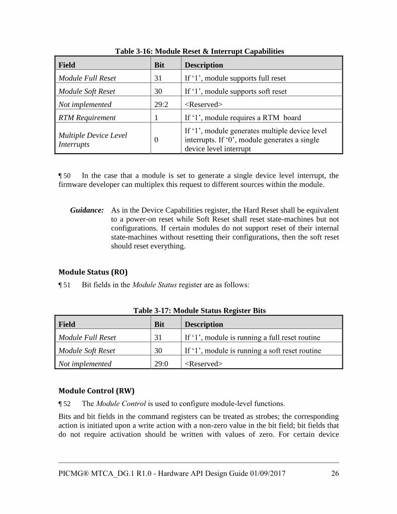
Table 3-16: Module Reset & Interrupt Capabilities
Field Bit Description
Module Full Reset 31 If ‘1’, module supports full reset
Module Soft Reset 30 If ‘1’, module supports soft reset
Not implemented 29:2 <Reserved>
RTM Requirement 1 If ‘1’, module requires a RTM board
Multiple Device Level
Interrupts 0
If ‘1’, module generates multiple device level
interrupts. If ‘0’, module generates a single
device level interrupt
¶ 50 In the case that a module is set to generate a single device level interrupt, the
firmware developer can multiplex this request to different sources within the module.
Guidance: As in the Device Capabilities register, the Hard Reset shall be equivalent
to a power-on reset while Soft Reset shall reset state-machines but not
configurations. If certain modules do not support reset of their internal
state-machines without resetting their configurations, then the soft reset
should reset everything.
Module Status (RO)
¶ 51 Bit fields in the Module Status register are as follows:
Table 3-17: Module Status Register Bits
Field Bit Description
Module Full Reset 31 If ‘1’, module is running a full reset routine
Module Soft Reset 30 If ‘1’, module is running a soft reset routine
Not implemented 29:0 <Reserved>
Module Control (RW)
¶ 52 The Module Control is used to configure module-level functions.
Bits and bit fields in the command registers can be treated as strobes; the corresponding
action is initiated upon a write action with a non-zero value in the bit field; bit fields that
do not require activation should be written with values of zero. For certain device

PICMG® MTCA_DG.1 R1.0 - Hardware API Design Guide 01/09/2017 27
capabilities, writing a value of ‘0’ in the bit field will disable the capability specified in
the mirror bit on the Device Capabilities register.
¶ 53 A read action of the control register reports the current state of the requested
action, with a 0 indicating “not running” or “complete”, depending on the circumstances.
The readback is guaranteed to change to match the state of the request upon the write, so
a read value of “complete” may always be interpreted to indicate the requested action
either completed or never ran – there will be no race condition between the write and the
readback.
¶ 54 Bit fields in the control register are as follows:
Table 3-18: Control Register Reset Operation
Field Bit Description
Module Full Reset 31 Writing ‘1’ will begin a hard reset routine
Module Soft Reset 30 Writing ‘1’ will begin a soft reset routine
Control Capabilities 29:0 <Reserved>
3.1.3.3 Module Interrupt Register Set
¶ 55 The following registers allow users to identify and configure the interrupts
generated by the module.
Interrupt ID (RO)
¶ 56 The Interrupt ID register shall identify the module at a device interrupts level.
Table 3-19 Interrupt ID Operation
Field Bit Description
Interrupt ID 31:0 Interrupt ID of the module
REQ 3.26 The bits in the register shall describe which device level interrupts can
be raised by this module. A value of ‘0’ in this register indicates that the
module does not generate device level interrupts.
¶ 57 The bit in the Module Capabilities register which determine if the module
generate multiple or single device level interrupts, determines if only 1 or multiple bits in
the Interrupt ID register are set to ‘1’.
Case ‘0’ - Module generates a single device level interrupt
¶ 58 Only one bit can be set to ‘1’ in the Interrupt ID register. The Module may have
multiple sources which can request a module interrupt. To identify the source, it is
necessary to read the information in the Module Interrupt Flag register.
PICMG® MTCA_DG.1 R1.0 - Hardware API Design Guide 01/09/2017 28
Guidance: Even without generating device level interrupts (either because the
current employ hardware firmware does not allow it or if the actual
device does not support it), interrupts generated by the different sources
in the module can still be used by polling the Device Interrupts Flag
register.
Case ‘1’ - Module generates multiple device level interrupts
¶ 59 Multiple bits can be set to ‘1’ in the Interrupt ID register. The Module does not
contain internal interrupt sources and therefore the module registers Module Interrupt
Mask, Flag and Active have no usage.
Interrupt Flag Clear (RW)
¶ 60 The Interrupt Flag Clear register allows, if necessary, resetting of the bits which
identify the generated device interrupts.
Table 3-20: Interrupt Flag Clear
Field Bit Description
Interrupt Flag Clear 31:0 A write ‘1’ strobe will clear the bit(s) which
identifies the generated interrupt.
Guidance: Clearing an interrupt flag can be used by the firmware as an interrupt
acknowledge.
¶ 61 Similar to the Interrupt ID register, the usage of this register depends on the value
of the bit in the Module Capabilities register which determines if the module generates
multiple or single device level interrupts.
Case ‘0’ - Module generates a single device level interrupt
¶ 62 The Interrupt Flag Clear register will clear the corresponding bit in the Module
Interrupts Flag and Active register of the module and the bits in the Device Interrupt
Flag and Active registers which identify the module.
Case ‘1’ - Module generates multiple device level interrupt
¶ 63 The Interrupt Flag Clear register will clear the corresponding bits in the Device
Interrupt Flag and Active registers.

PICMG® MTCA_DG.1 R1.0 - Hardware API Design Guide 01/09/2017 29
¶ 64 The following registers are only meaningful when the module is configured to
generate a single device level interrupt. Otherwise they have no effect on module
operation.
Module Interrupt Mask (RW)
¶ 65 The Module Interrupt Mask register configures which source interrupts are
enable.
Table 3-21: Interrupt Mask
Field Bit Description
Interrupt Mask 31:0 A bit field of ‘1’ enables source interrupts
assigned to that bit.
Module Interrupt Flag (RO)
¶ 66 The Module Interrupt Flag register shall report which source interrupts have been
requested. The bits in this register are masked by the Module Interrupt Mask.
Table 3-22: Interrupt Flags
Field Bit Description
Interrupt Flag 31:0 If a bit field is ‘1’, the source interrupt assigned to
that bit was raised.
Module Interrupt Active (RO)
REQ 3.27 The Module Interrupt Active register shall report which source
interrupts have been requested. The bits in this register are not
masked by the Module Interrupt Mask.
Table 3-23: Interrupt Active
Field Bit Description
Interrupt Active 31:0 If a bit field is ‘1’, the source interrupt assigned to
that bit was raised.
Guidance: This register can be used for polling source interrupts when these are
disabled in the Interrupt Mask.
PICMG® MTCA_DG.1 R1.0 - Hardware API Design Guide 01/09/2017 30
¶ 67 Module-specific implementation registers follow immediately after the Interrupt
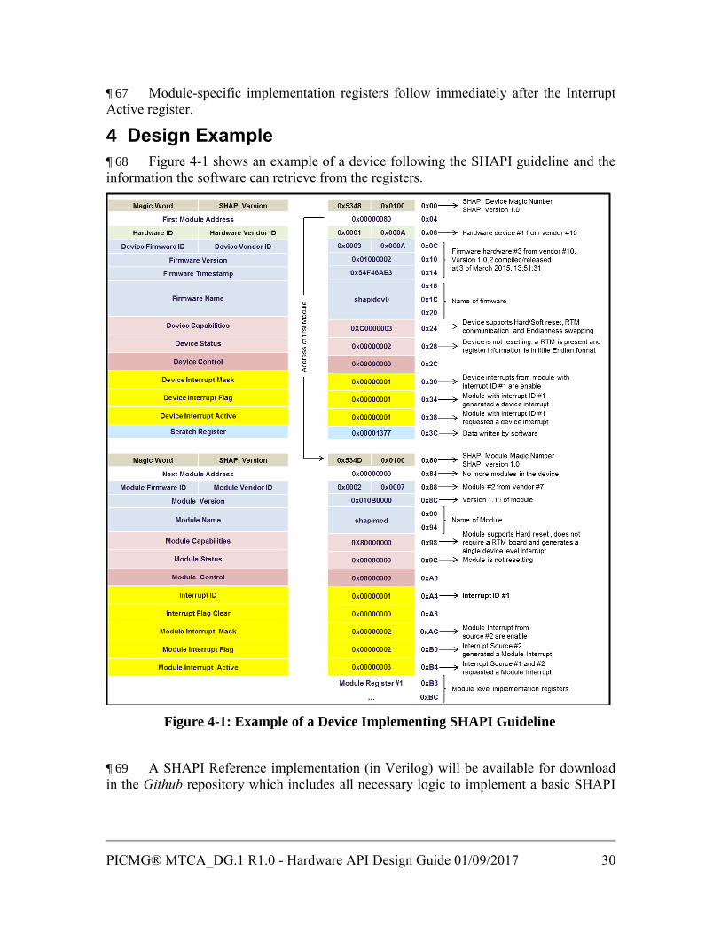
Active register.
4 Design Example
¶ 68 Figure 4-1 shows an example of a device following the SHAPI guideline and the
information the software can retrieve from the registers.
¶ 69 A SHAPI Reference implementation (in Verilog) will be available for download
in the Github repository which includes all necessary logic to implement a basic SHAPI
Figure 4-1: Example of a Device Implementing SHAPI Guideline

PICMG® MTCA_DG.1 R1.0 - Hardware API Design Guide 01/09/2017 31
device module register set together with a library to build application specific registers.
See https://github.com/MicroTCA/MTCA.4.
5 Standard Module Example
¶ 70 The following section describes an example of a standard SHAPI Module. These
are modules which are not unique to a particular vendor and are commonly used within
different instructions. Following the spirit of the SHAPI guidelines, a separate guideline
shall be written for each of these modules which define the registers that the module
implements. The Vendor ID for these modules is fixed to ‘0’.
A standard SHAPI module for DMA is described in this section.
Information in the SHAPI Module Standard Register Set
REQ 5.1 The Module Firmware ID for DMA is 1 and, as stated before,
because this is a standard SHAPI Module the Vendor ID shall be 0.
REQ 5.2 The remaining registers of the Standard Register set report the same
information as any other SHAPI Modules. The following registers
shall follow the SHAPI Module standard register set:
¶ 71 When the device requires a RTM board (see section 3.1.3.2) to perform a DMA
transfer, the device developer should implement the logic so that the transfer does not
occur if no RTM is detected (when this is possible). In the case a RTM is removed during
a DMA transfer, it is recommended that the device generates a interrupt informing the
device driver to stop the transfer.
DMA Capabilities (RO)
¶ 72 Bit fields in the DMA Capabilities register are as follows:
Table 5-1: DMA Capabilities Register
Field Bit Description
Not implemented 31:6 <Reserved>
RTM Requirement 5 If ‘1’, DMA requires a RTM board to operate
correctly
Data Transfer 4 If ‘1’, To/From Data Transfers registers report the
size of data that has been transfer
Simultaneous Read/Write
Transfers 3
If ‘1’, DMA supports simultaneous write and read
transfers.
To Device Transfer 2 If ‘1’, DMA supports transfers to the device
From Device Transfer 1 If ‘1’, DMA supports transfers from the device

PICMG® MTCA_DG.1 R1.0 - Hardware API Design Guide 01/09/2017 32
Endianness Available 0 If ‘1’, it’s possible to swap between DMA data
endianness formats
Guidance: The DMA Endianness configuration is independent of the Device
Endianness configuration.
DMA Status (RO)
¶ 73 Bit fields in the DMA Status register are as follows:
Field Bit Description
Not implemented 31:8 <Reserved>
To Device Timeout 7 If ‘1’, last DMA write transfer ended due to a
timeout.
To Device Done 6 If ‘1’, last DMA transfer to the device has
finished.
To Device Active 5 If ‘1’, DMA is currently transferring data to the
Device.
From Device Timeout 4 If ‘1’, last DMA transfer from device ended due
to a timeout.
From Device Done 3 If ‘1’, last DMA transfer from device has
finished.
From Device Active 2 If ‘1’, DMA is currently transferring data from
the Device.
DMA Initialization Done 1 If ‘1’, DMA controller initialization is finished
and can begin issuing commands to the memory.
Endianness 0 ‘0’ – little-endian format.
‘1’ – big-endian format
DMA Control (RW)
Bit fields in the DMA control register are as follows:
Field Bit Description
Not implemented 31:3 <Reserved>
Start To Device Transfer 2 A write ‘1’ strobe to this bit will begin transfer of
data to the Device.
Start From Device Transfer 1 A write ‘1’ strobe to this bit will begin transfer of
data from the Device.
Endianness 0 ‘0’ – little-endian format.

PICMG® MTCA_DG.1 R1.0 - Hardware API Design Guide 01/09/2017 33
‘1’ – big-endian format
From Device Destination (RW)
¶ 74 The From Device Destination shall compromise two 32-bit words which defines
the starting address to which the data from the DMA shall start to be written (usually
CPU system memory space).
From Device Source (RW)
¶ 75 The From Device Source shall compromise two 32-bit words which defines the
memory address offset to the DMA transfer located in the device.
From Device Data Size (RW)
¶ 76 The From Device Data Size shall define the size of data to be transfer from the
Device (in bytes).
From Device Data Transfer (RO)
¶ 77 The From Device Data Transfer shall report the size of data transfer in the last
From Data Transfer operation (in bytes).
To Device Destination (RW)
¶ 78 The To Device Destination shall compromise two 32-bit words which defines the
starting device memory address to which the data from the DMA shall start to be written.
To Device Source (RW)
¶ 79 The To Device Source shall compromise two 32-bit words which defines the
memory address offset to the DMA transfer (usually the CPU system memory space).
To Device Data Size (RW)
¶ 80 The To Device Source shall define the size of data to be transfer to the Device (in
bytes).
To Device Data Transfer (RO)
¶ 81 The To Device Data Transfer shall report the size of data that has been transferred
in the last To Device Transfer operation (in bytes).
Guidance: The driver should not expose these registers to the user space to avoid
misuse.
Guidance: For DMA controllers supporting different channels, each one can be
treated as a separate interrupt source, therefore having a single interrupt
for the DMA standard module, or instantiate for each channel a DMA
standard module and assign different interrupts for each module.
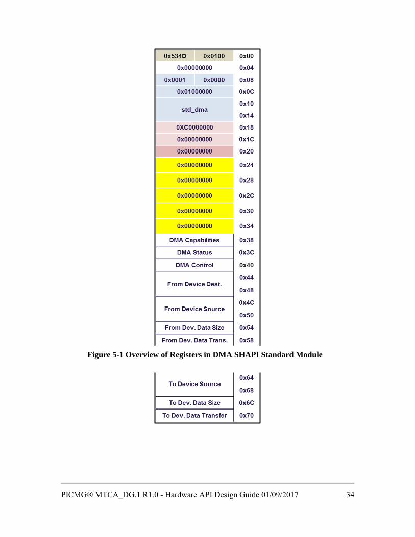
PICMG® MTCA_DG.1 R1.0 - Hardware API Design Guide 01/09/2017 34
Figure 5-1 Overview of Registers in DMA SHAPI Standard Module
PICMG® MTCA_DG.1 R1.0 - Hardware API Design Guide 01/09/2017 35
6 Example of Interrupts
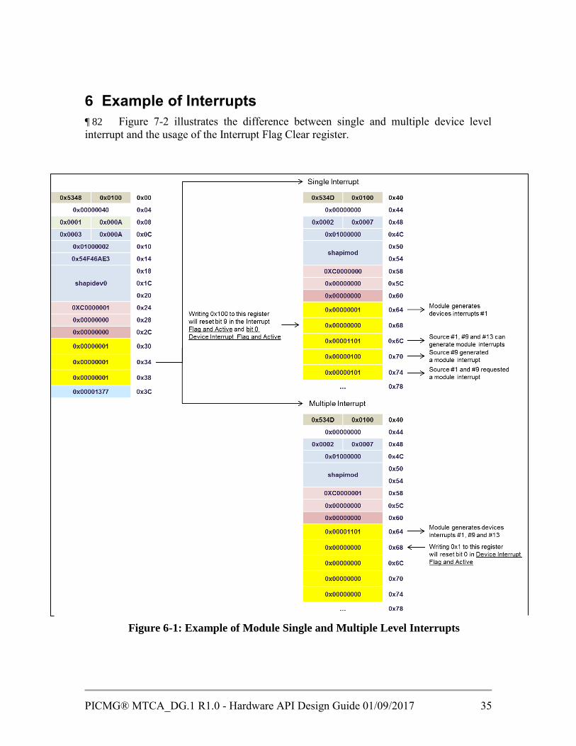
¶ 82 Figure 7-2 illustrates the difference between single and multiple device level
interrupt and the usage of the Interrupt Flag Clear register.
Figure 6-1: Example of Module Single and Multiple Level Interrupts

PICMG® MTCA_DG.1 R1.0 - Hardware API Design Guide 01/09/2017 36
7 Revision History
Table 7-1 Revision History
Revision Date Description
R1.0 01/09/2017 Initial Release

PICMG® MTCA_DG.1 R1.0 - Hardware API Design Guide 01/09/2017 37
8 Table of Requirements
REQ 3.1 The fundamental paradigm for device access defined by the SHAPI shall be
an addressable I/O space through which various device functions may be managed.
That paradigm applies at both the hardware and software levels identified in Figure
1. 11
REQ 3.2 All Registers shall be 32-bits wide and presented at the software API in
native processor byte-order. .................................................................................................. 12
REQ 3.3 Devices shall export a logical access API which comprises an addressable
space through which registers may be accessed. .................................................................. 12
REQ 3.4 Devices shall map all configuration, control, and data flow functions into
the addressable register API.................................................................................................. 13
REQ 3.5 Within hardware devices, register sets that represent monolithic data
elements wider than 32-bits at successive addresses shall be accessed in little-endian
word-order............................................................................................................................. 13
REQ 3.6 Desired: Devices shall minimize the use of stream-oriented “command
sequences” and instead, implement controls through arrays of static configuration
and control registers. ............................................................................................................. 13
REQ 3.7 The Magic Word and SHAPI Version Register shall report a 16-bit wide
fixed number, which indicates that SHAPI is implemented. Furthermore, it shall
indicate the SHAPI version implemented. The bits in the register are defined as
follows: ................................................................................................................................. 15
REQ 3.8 The First Module Address shall report the absolute address of the first
module in the firmware. Each module register address space starts with a standard
set as specified in 3.1.3. A value of ‘0’ shall be reserved to designate that no
modules are implemented. .................................................................................................... 15
REQ 3.9 The Hardware ID and Hardware Vendor ID Register shall report a unique
device identifier for each unique device vendor. The register shall comprise two 16-
bit fields, as follows: ............................................................................................................. 15
REQ 3.10 The Hardware ID shall be assigned by the vendor or, in the case of a
“standard” API, by PICMIG. ................................................................................................ 16
REQ 3.11 The Hardware Vendor ID shall be unique to each board vendor and shall
identify the entity responsible for the board design. The Hardware Vendor ID shall
be assigned by PICMIG. ....................................................................................................... 16
REQ 3.12 A Hardware Vendor ID value of 0 shall be reserved to designate devices
that implement an agreed-upon “standard” API that is not unique to a particular
vendor. 16
REQ 3.13 The Device Firmware ID and Device Vendor ID shall report a unique device
firmware identifier. The firmware identifier shall comprise of two 16-bit fields, as
follows: ................................................................................................................................. 16

PICMG® MTCA_DG.1 R1.0 - Hardware API Design Guide 01/09/2017 38
REQ 3.14 The Device Firmware ID shall be assigned by the firmware vendor. ...................... 16
REQ 3.15 Similar to the Hardware Vendor ID, the Device Vendor ID shall be unique
to each firmware vendor and identify the entity responsible for the firmware. The
Device Vendor ID shall be assigned by PICMIG. ................................................................ 16
REQ 3.16 When a version field is increased, the corresponding lower priority fields
shall be reset. ........................................................................................................................ 17
REQ 3.17 The Firmware Timestamp shall report the UNIX timestamp of the
firmware version currently running on the device. The value shall be reported in
unsigned 32 bit integer format. ............................................................................................. 17
REQ 3.18 The Device Capabilities shall report the functionalities supported by the
device. Bits in this register shall be as follows: .................................................................... 18
REQ 3.19 The Magic Word and SHAPI Version Register shall report a 16-bit wide
fixed number, which indicates, that SHAPI is implemented. Furthermore, it shall
indicate the SHAPI version implemented. The usage of the bits in the register is
defined as follows: ................................................................................................................ 22
REQ 3.20 The Next Module Address shall report the absolute address of the following
module in the firmware. Each module register address space starts with a standard
set as specified in 3.1.3. A value of ‘0’ shall be reserved to designate that no more
modules are implemented. .................................................................................................... 23
REQ 3.21 The Module Firmware and Vendor ID shall report the module firmware
identifier. The firmware identifier shall comprise of two 16-bit fields, as follows: ............ 23
REQ 3.22 The Module Firmware ID shall be assigned by the firmware vendor. ..................... 23
REQ 3.23 The Module Vendor ID shall be unique to each firmware vendor and identify
the entity responsible for the firmware. The Module Vendor ID shall be assigned by
PICMIG................................................................................................................................. 23
REQ 3.24 A value of ‘0’ shall be reserved to designate vendors implement an
agreed-upon “standard” API that is not unique to a particular vendor. This includes
modules that are responsible for DMA transfers or upload of firmware to the device.
Although the Standard Set of these modules will have a similar structure to the one
described in this guideline, the information on the Capabilities, Status and Control
registers will be described in the guideline that defines these modules. .............................. 23
REQ 3.25....................................................................................................................................... 25
REQ 3.26 The bits in the register shall describe which device level interrupts can be
raised by this module. A value of ‘0’ in this register indicates that the module does
not generate device level interrupts. ..................................................................................... 27
REQ 3.27 The Module Interrupt Active register shall report which source interrupts
have been requested. The bits in this register are not masked by the Module
Interrupt Mask. ..................................................................................................................... 29

PICMG® MTCA_DG.1 R1.0 - Hardware API Design Guide 01/09/2017 39
REQ 5.1 The Module Firmware ID for DMA is 1 and, as stated before, because this is
a standard SHAPI Module the Vendor ID shall be 0. .......................................................... 31
REQ 5.2 The remaining registers of the Standard Register set report the same
information as any other SHAPI Modules. The following registers shall follow the
SHAPI Module standard register set: ................................................................................... 31