Standard Bipolar Applications - UT Arlington – UTA PNP transistor
43
Standard Bipolar Process
Transcript of Standard Bipolar Applications - UT Arlington – UTA PNP transistor

Standard Bipolar Process
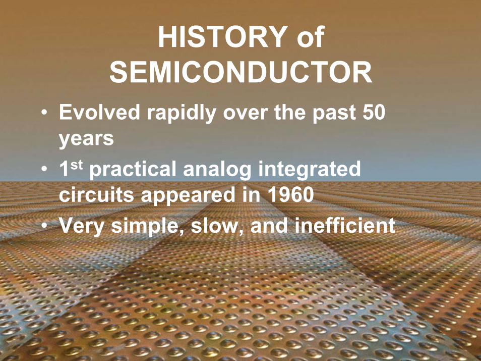
• Evolved rapidly over the past 50years
• 1st practical analog integratedcircuits appeared in 1960
• Very simple, slow, and inefficient
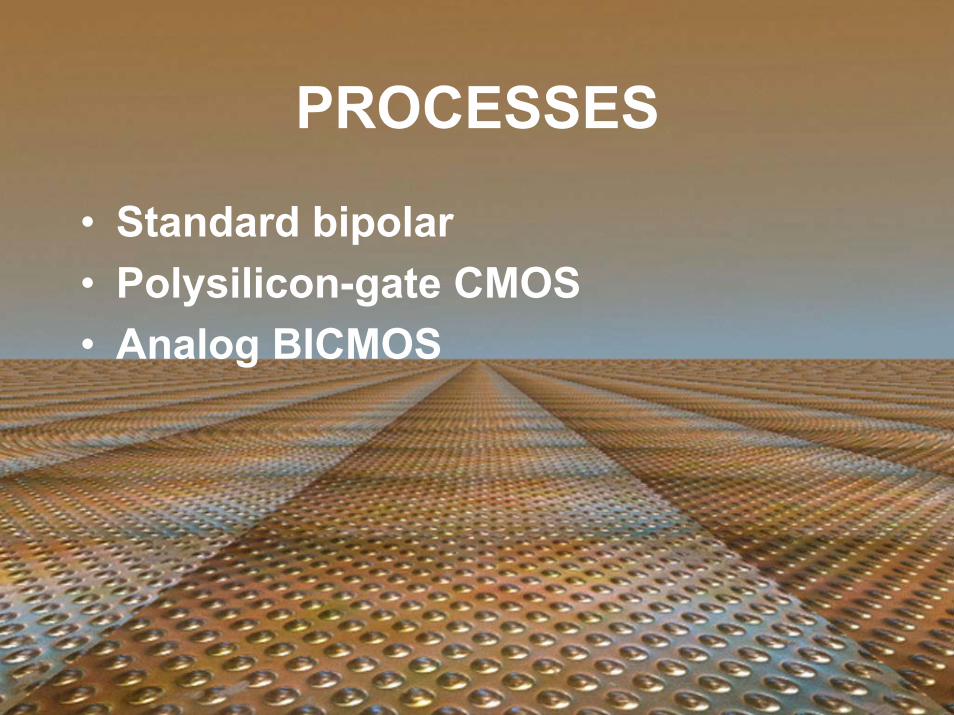
• Standard bipolar• Polysilicon-gate CMOS• Analog BICMOS
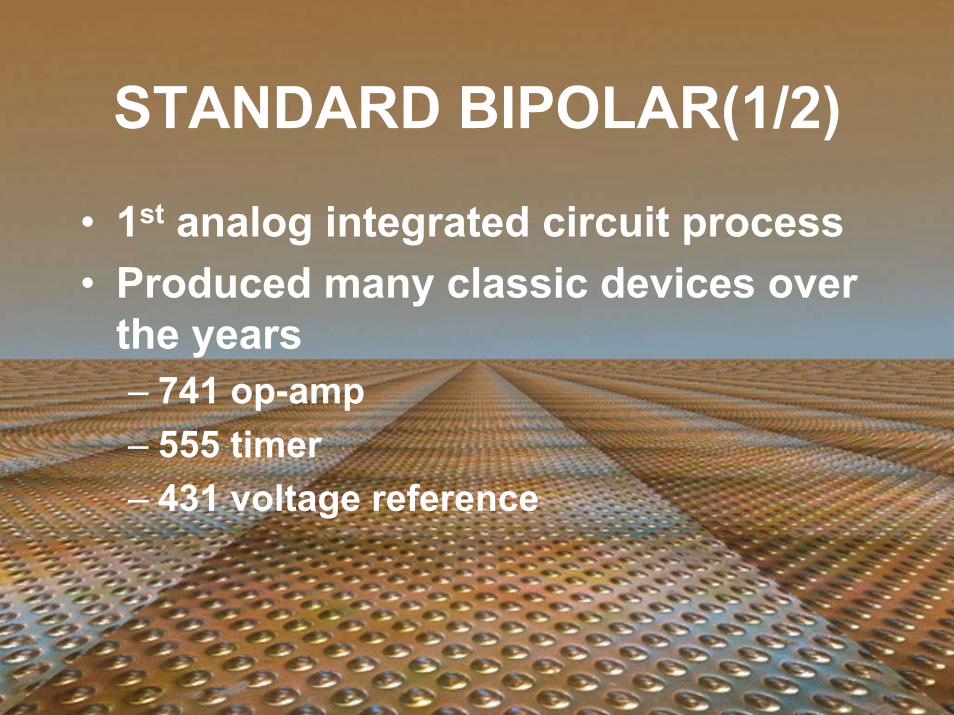
• 1st analog integrated circuit process• Produced many classic devices over
the years– 741 op-amp– 555 timer– 431 voltage reference
• Seldom used for new designs• Knowledge from standard bipolar will
never become obsolete• Same devices, parasitic
mechanisms, design tradeoffs,layout principles
• Shaped to optimize the NPN at theexpense of the PNP transistors
• NPN will outperform PNP bye morethen 2:1
• Early processes optimized NPN andavoided PNP transistors altogether
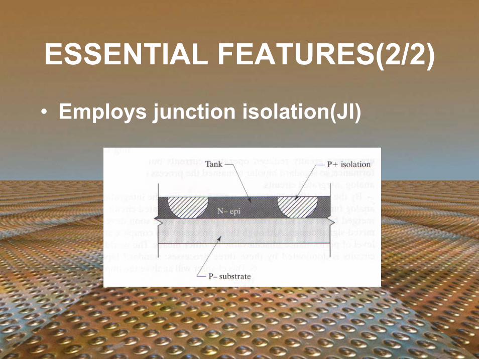
• Employs junction isolation(JI)

• Reverse-biased JIs exhibit enoughcapacitance to slow the operation ofmany circuits
• High temperatures can causesignificant leakage currents
• Unusual operating conditions canforward bias the JIs and injectminority carriers into the substrate
• Successfully fabricate most circuits• Considerably cheaper than any of its
alternatives

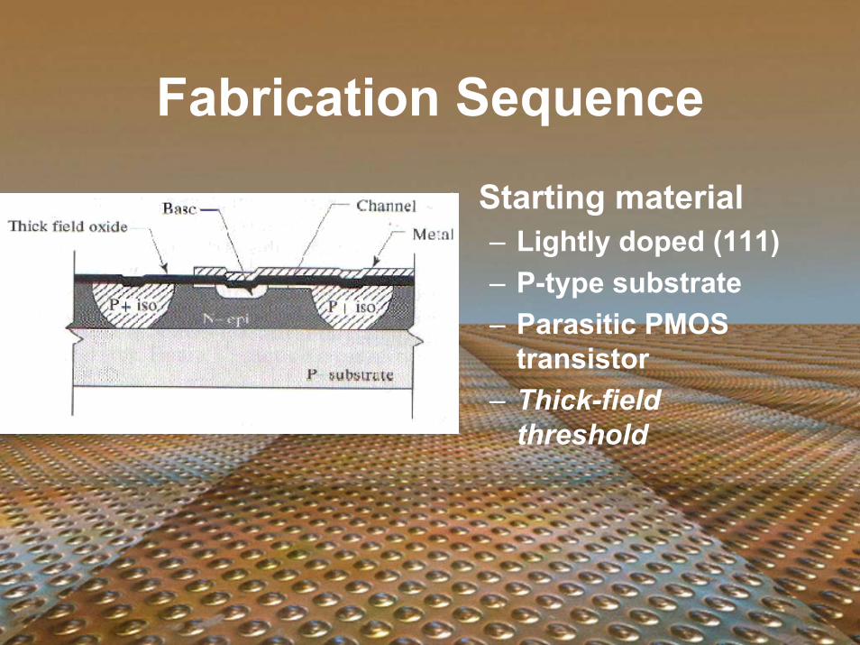
• Starting material– Lightly doped (111)– P-type substrate– Parasitic PMOS
transistor– Thick-field
threshold
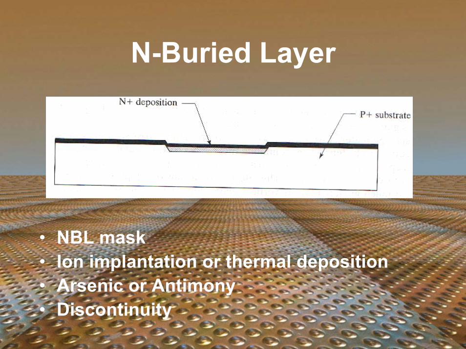
• NBL mask• Ion implantation or thermal deposition• Arsenic or Antimony• Discontinuity

• 25m of n-type epi• 45º discontinuity propagation• NBL shadow• Lateral shift = thickness of epi
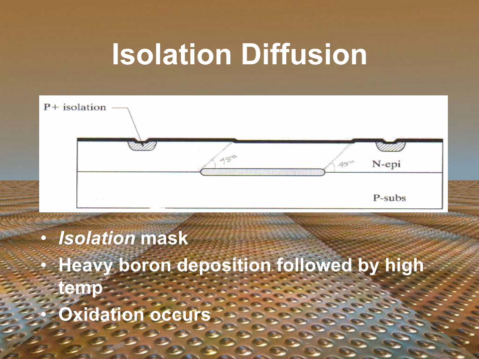
• Isolation mask• Heavy boron deposition followed by high
temp• Oxidation occurs
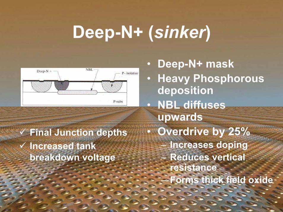
sinker
Final Junction depths Increased tank
breakdown voltage
• Deep-N+ mask• Heavy Phosphorous
deposition• NBL diffuses
upwards• Overdrive by 25%– Increases doping– Reduces vertical
resistance– Forms thick field oxide
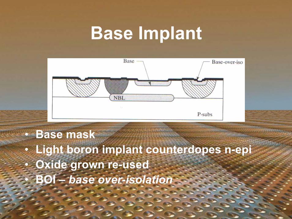
• Base mask• Light boron implant counterdopes n-epi• Oxide grown re-used• BOI – base over-isolation
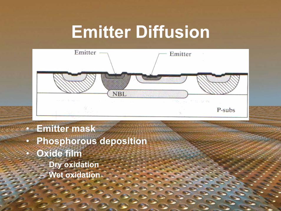
• Emitter mask• Phosphorous deposition• Oxide film
– Dry oxidation– Wet oxidation
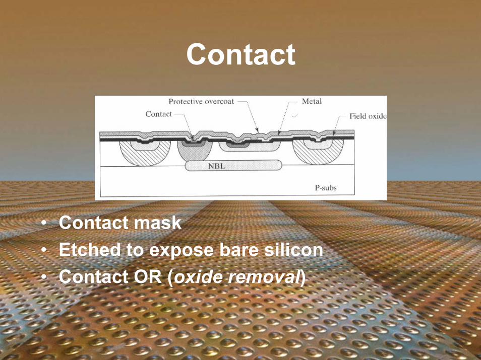
• Contact mask• Etched to expose bare silicon• Contact OR (oxide removal)
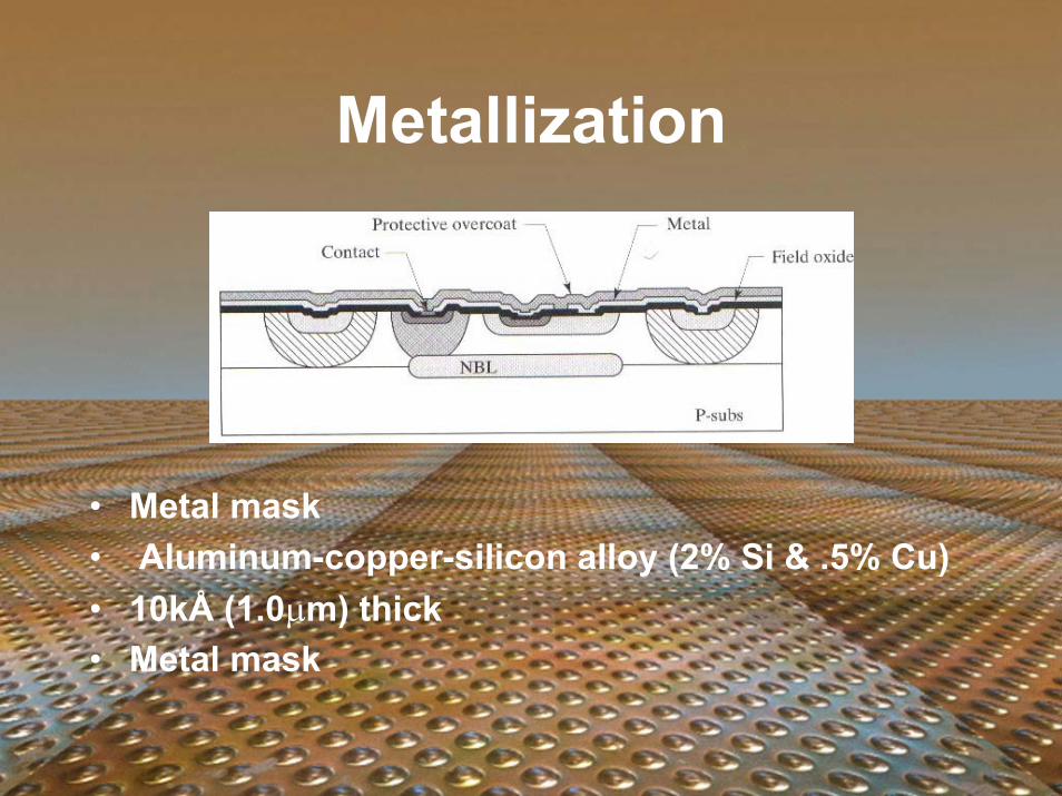
• Metal mask• Aluminum-copper-silicon alloy (2% Si & .5% Cu)• 10kÅ (1.0m) thick• Metal mask
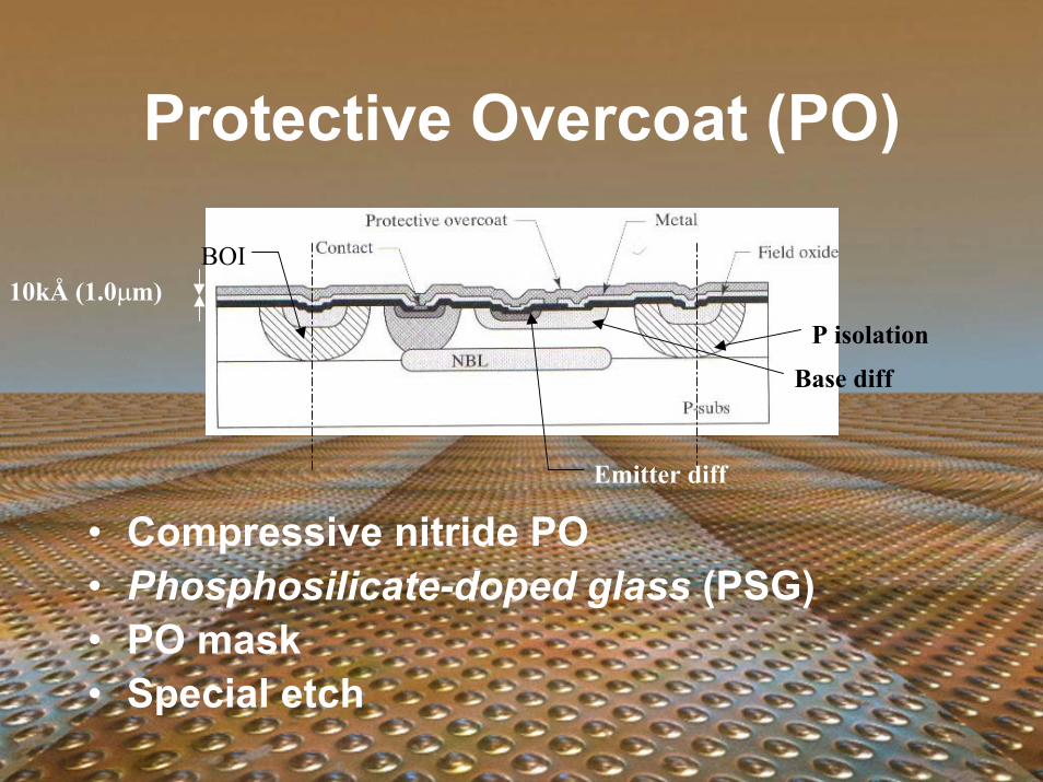
• Compressive nitride PO• Phosphosilicate-doped glass (PSG)• PO mask• Special etch
Base diff
Emitter diff
BOI
P isolation10kÅ (1.0m)
Bipolar NPN transistorsTwo types of PNP transistors:
Substrate + LateralDiffused resistors
Capacitors
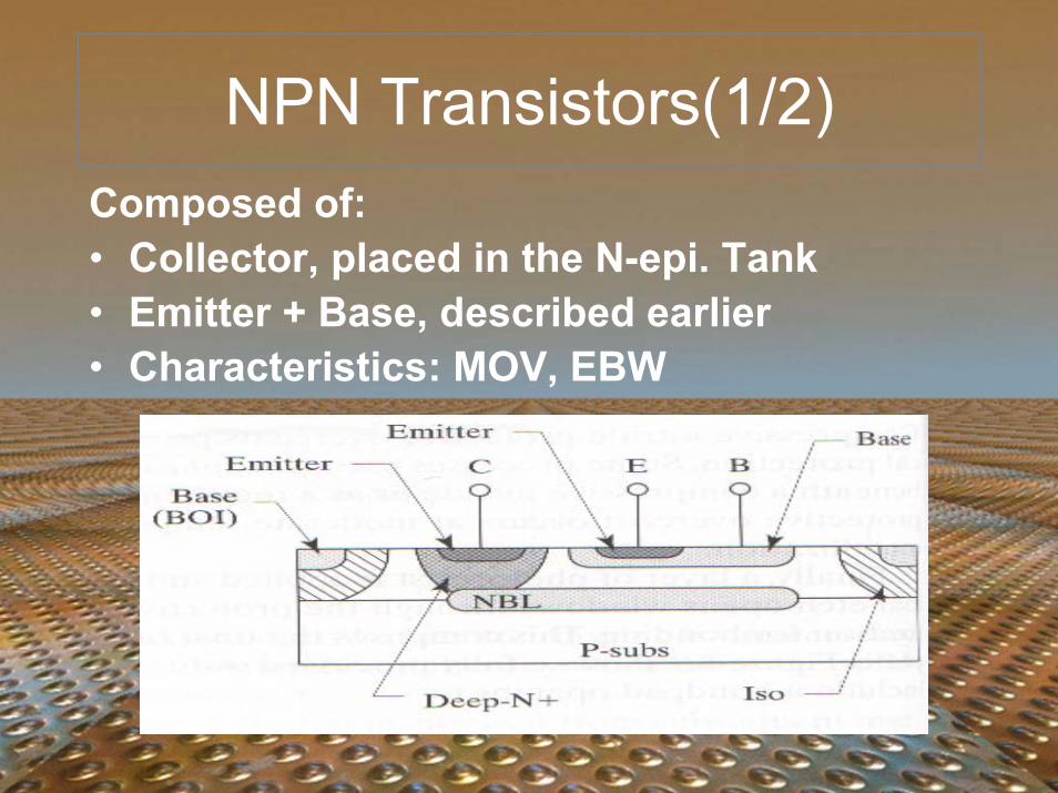
Composed of:• Collector, placed in the N-epi. Tank• Emitter + Base, described earlier• Characteristics: MOV, EBW
• Maximum Operating Voltage, up to (50 –80v)
• Effective Base Width: E & B width• Diode formation: CB Shorted Diode• B & C for anode, E for Cathode• Drawbacks: Low breakdown VEBO• Alternative: Act as a Zener diode• NPN is the best to be designed by this
process and shows a good performance
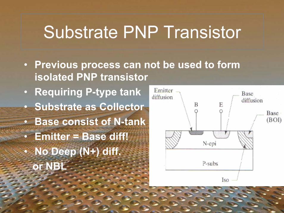
• Previous process can not be used to formisolated PNP transistor
• Requiring P-type tank• Substrate as Collector• Base consist of N-tank• Emitter = Base diff!• No Deep (N+) diff. or NBL
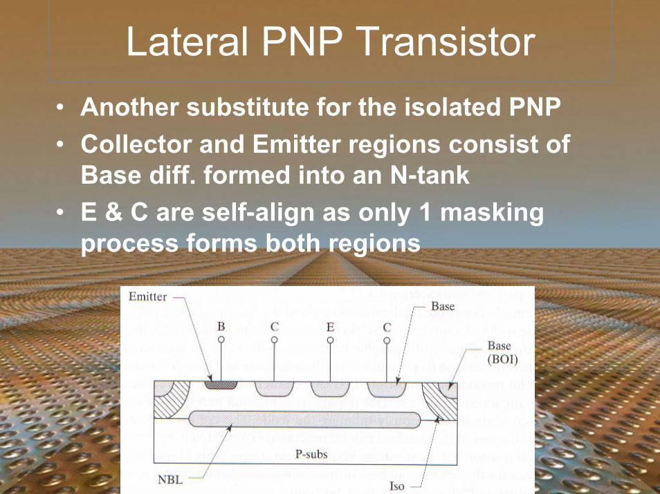
• Another substitute for the isolated PNP• Collector and Emitter regions consist of
Base diff. formed into an N-tank• E & C are self-align as only 1 masking
process forms both regions
• Based on Characteristics Sheet resistanceprinciple:resistance measured across asquare of the material connected onopposite sides (Ω / ? )
• Diffusion causes non uniform doping• 3 types of resistors:
Base ResistorEmitter ResistorPinch Resistor
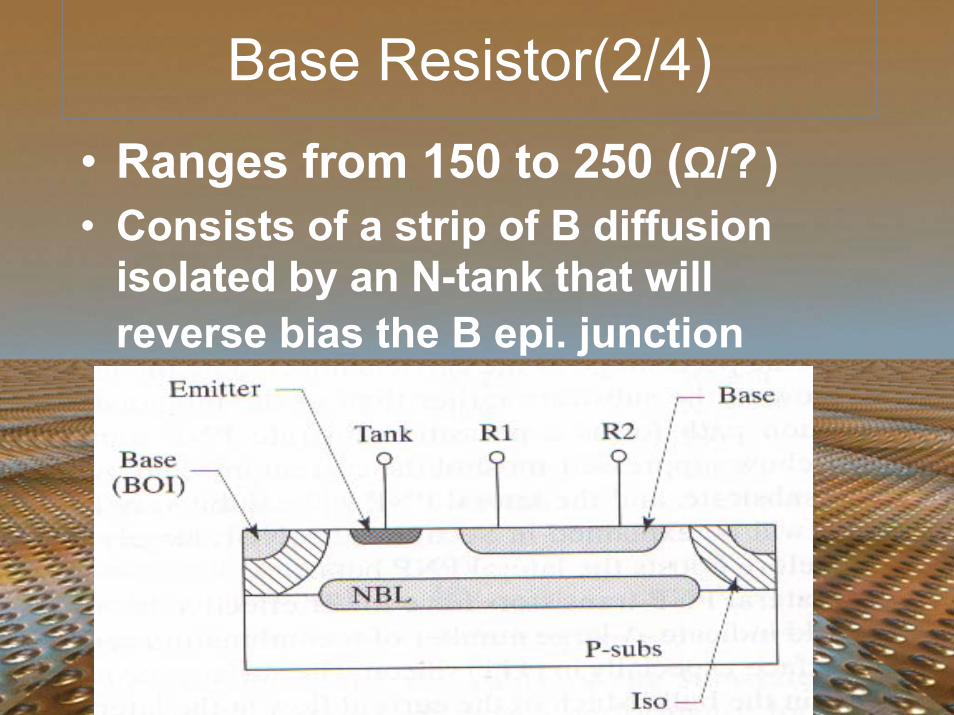
Ω/ )• Consists of a strip of B diffusion
isolated by an N-tank that willreverse bias the B epi. junction

•A strip of E diff. Isolated by B diff. enclosed within the N-tank•B region to reverse bias E-B junc.•E sheet resistance less than 10 Ω/ )
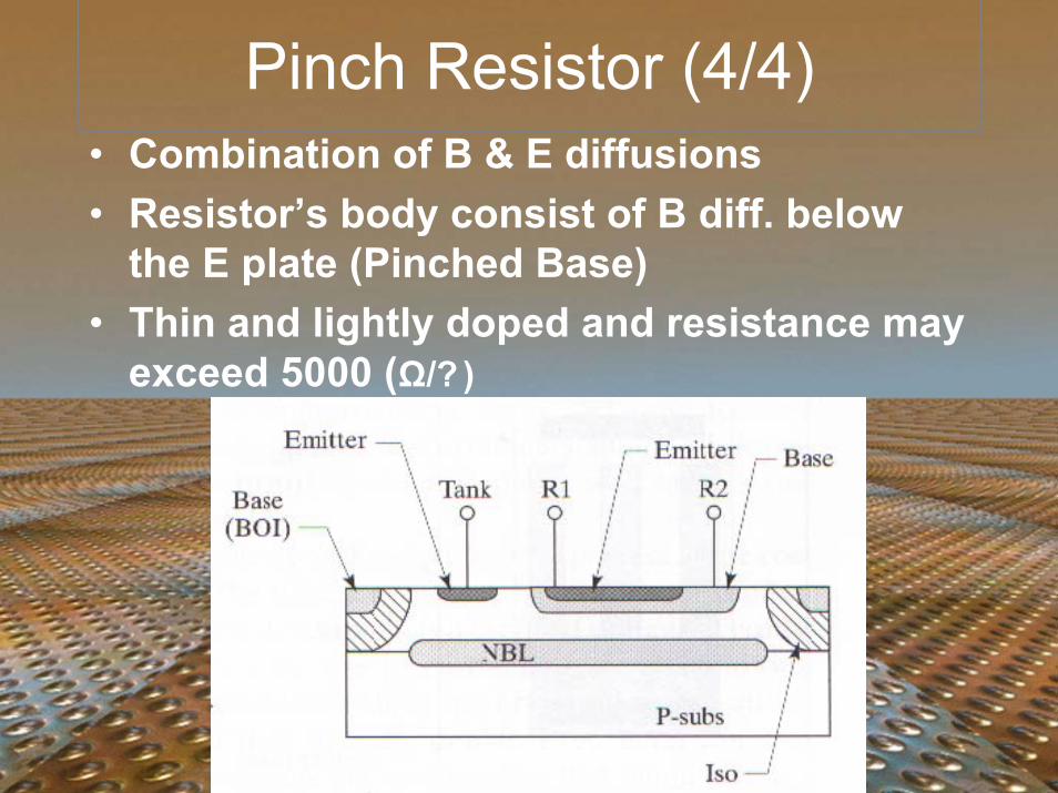
• Combination of B & E diffusions• Resistor’s body consist of B diff. below
the E plate (Pinched Base)• Thin and lightly doped and resistance may
exceed 5000 (Ω/? )
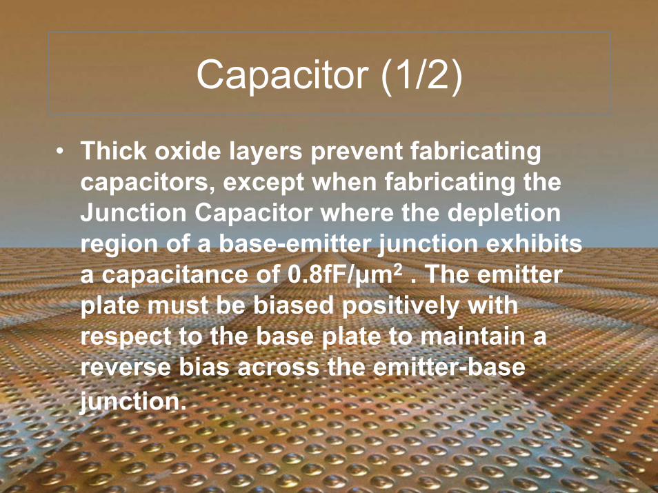
• Thick oxide layers prevent fabricatingcapacitors, except when fabricating theJunction Capacitor where the depletionregion of a base-emitter junction exhibitsa capacitance of 0.8fF/µm2 . The emitterplate must be biased positively withrespect to the base plate to maintain areverse bias across the emitter-basejunction.
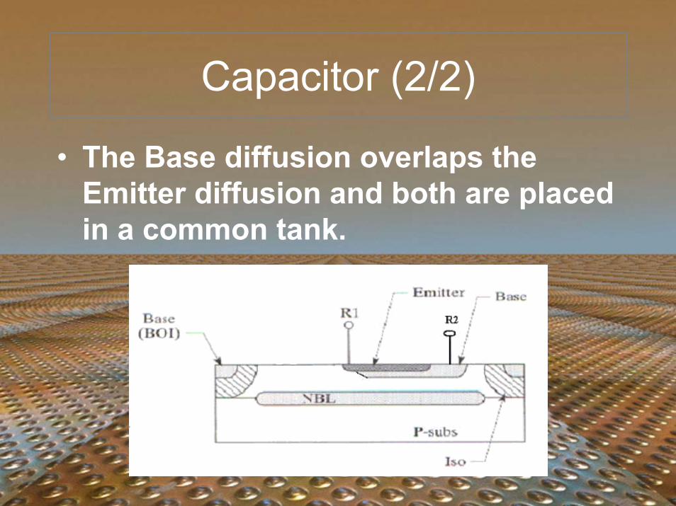
• The Base diffusion overlaps theEmitter diffusion and both are placedin a common tank.
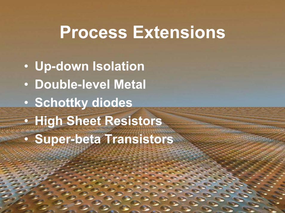
• Up-down Isolation• Double-level Metal• Schottky diodes• High Sheet Resistors• Super-beta Transistors
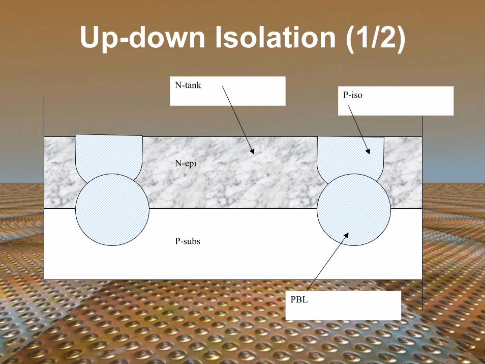
P-iso
N-epi
P-subs
PBL
N-tank
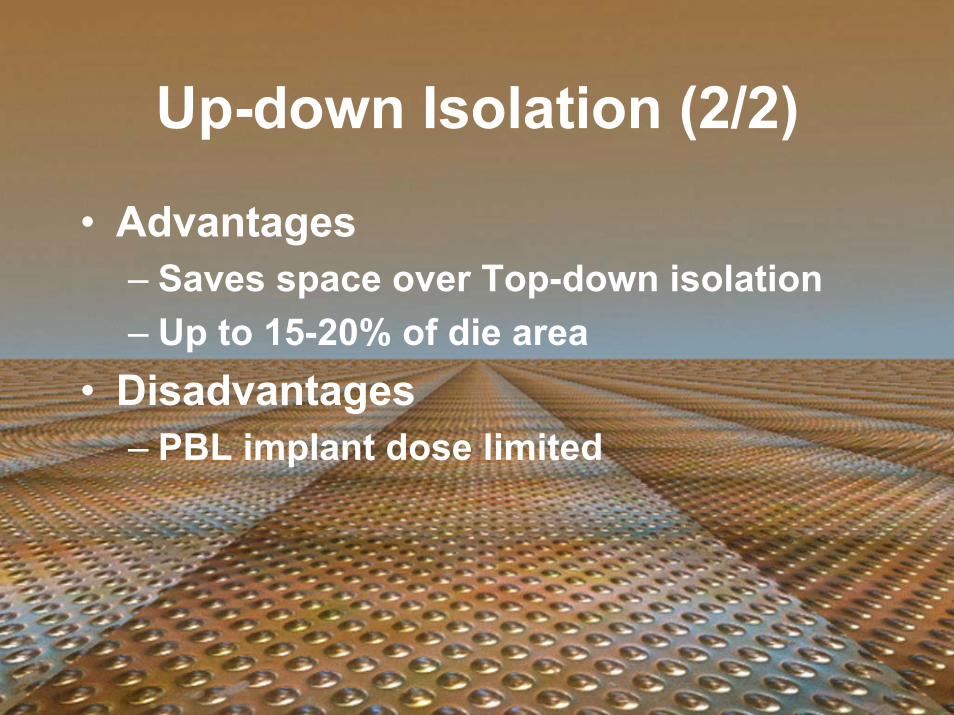
• Advantages– Saves space over Top-down isolation– Up to 15-20% of die area
• Disadvantages– PBL implant dose limited

• Advantages– Reduces die area by 30% over single-level metal– Allows component standardization
• Disadvantages– Requires two extra masks: vias and metal-2– P-Buried Layer (PBL) requires additional steps– Costly
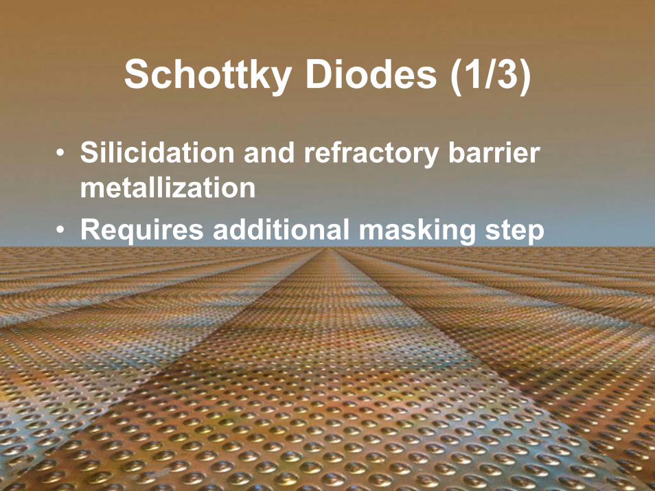
• Silicidation and refractory barriermetallization
• Requires additional masking step
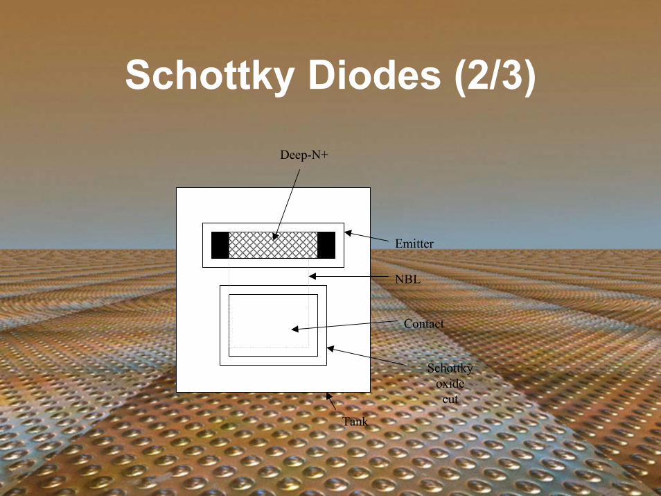
Deep-N+
Emitter
NBL
Contact
Schottkyoxide
cut
Tank
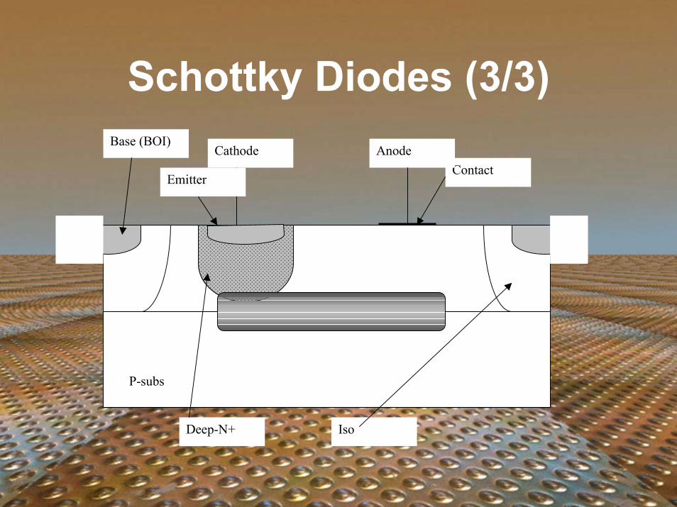
ContactCathode Anode
P-subsP-subs
Deep-N+ Iso
Emitter
Base (BOI)
• Compensates for base diffusion andpinch resistor
• Beta increased by narrowing basewidth
• Betas of 1000 to 3000
• The Art of Analog Layout, AlanHastings