ST7 TECHNICAL TRAINING - st.com · ¾6 internal registers: Accumulator (A), X and Y index...
59
ST7 TECHNICAL TRAINING 1. INTRODUCTION 2. CORE 3. ADDRESSING MODES 4. ASSEMBLY TOOLCHAIN 5. STVD7 DEBUGGER 6. HARDWARE TOOLS 7. PERIPHERALS 8. ST-REALIZER II 9. C TOOLCHAINS
Transcript of ST7 TECHNICAL TRAINING - st.com · ¾6 internal registers: Accumulator (A), X and Y index...

ST7 TECHNICAL TRAINING1. INTRODUCTION2. CORE3. ADDRESSING MODES4. ASSEMBLY TOOLCHAIN5. STVD7 DEBUGGER6. HARDWARE TOOLS7. PERIPHERALS8. ST-REALIZER II9. C TOOLCHAINS
ST7 CORE
WATCHDOG
LOWPOWER
MODES
INTERNAL
REGISTERS
ST7STACK
CLOCK
CONTROLLER
INTERRUPTS
MEMORY
SPACE
RESET
SYSTEM
LVD

ST7 CORE General Description
• The ST7 core (von neuman architecture) is built around:An 8-bit Arithmetic and Logic Unit (ALU)6 internal registers: Accumulator (A), X and Y index registers, Program Counter (PC), the Stack Pointer (SP) and the Code Condition register (CC)A controller block
• It interfaces with:An on-chip oscillatorA reset blockAddress and data buses to access memories and peripheralsAn interrupt controller

ISPSEL/ Vpp/ICCSEL
AD
DR
ESS B
US
DA
TA B
US
RAM
Program memory
WatchdogLVDEnhancedReset
Internal CLOCK
SP
PCHPCL
CONTROL
8 -BIT ALU
AccuIndex XIndex Y
CC
Mutli oscillatorClock controller
OSCin
OSCout
RESET
ST7 COREBlock Diagram
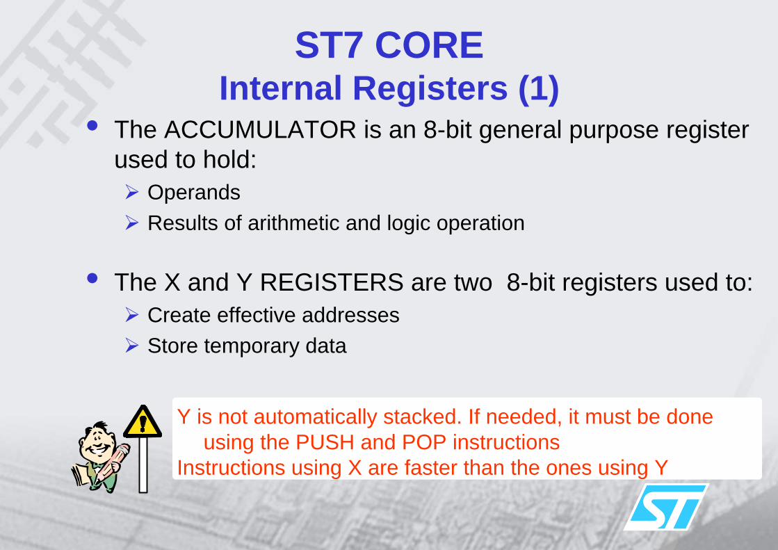
ST7 COREInternal Registers (1)
• The ACCUMULATOR is an 8-bit general purpose register used to hold:
OperandsResults of arithmetic and logic operation
• The X and Y REGISTERS are two 8-bit registers used to:Create effective addressesStore temporary data
Y is not automatically stacked. If needed, it must be done using the PUSH and POP instructions
Instructions using X are faster than the ones using Y
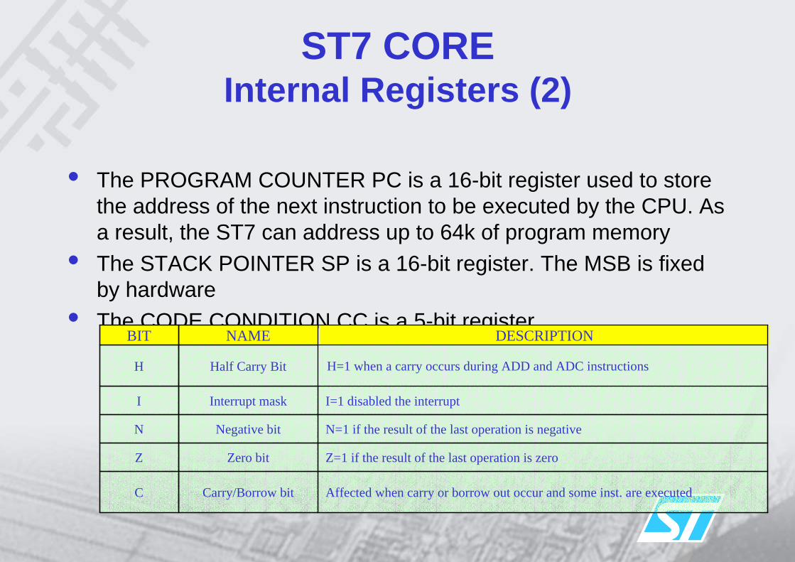
ST7 COREInternal Registers (2)
• The PROGRAM COUNTER PC is a 16-bit register used to store the address of the next instruction to be executed by the CPU. As a result, the ST7 can address up to 64k of program memory
• The STACK POINTER SP is a 16-bit register. The MSB is fixed by hardware
• The CODE CONDITION CC is a 5-bit register
Affected when carry or borrow out occur and some inst. are executedCarry/Borrow bitC
Z=1 if the result of the last operation is zeroZero bitZ
N=1 if the result of the last operation is negativeNegative bitN
I=1 disabled the interruptInterrupt maskI
H=1 when a carry occurs during ADD and ADC instructionsHalf Carry BitH
DESCRIPTIONNAMEBIT
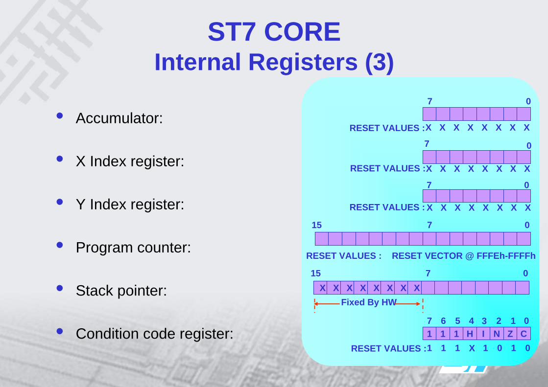
ST7 COREInternal Registers (3)
• Accumulator:
• X Index register:
• Y Index register:
• Program counter:
• Stack pointer:
• Condition code register:
7 0
RESET VALUES :X X X X X X X X
0
XXXXXXXXRESET VALUES :
7 0
RESET VALUES : XX X X X X X X
RESET VALUES : RESET VECTOR @ FFFEh-FFFFh
0715
07 6 5 4 3 2 1
RESET VALUES : 0101X111
7
1 11 H I CZN
15 7 0
Fixed By HWX X XX XXXX

ST7 COREStack manipulation (1)
• Purpose:Save the CPU context during subroutine calls or interruptsSave temporary user's data (PUSH and POP instructions)
• In case of overflow (lower limit exceeded):SP rolls over to the higher addressValue at the higher address is overwritten so lost Stack overflow is not indicated
Lower Address
Higher Address
Push YCall subroutines or interrupt
Pop YReturn from subroutines or interrupt
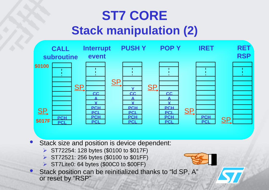
ST7 COREStack manipulation (2)
• Stack size and position is device dependent:ST72254: 128 bytes ($0100 to $017F)ST72521: 256 bytes ($0100 to $01FF)ST7Lite0: 64 bytes ($00C0 to $00FF)
• Stack position can be reinitialized thanks to “ld SP, A” or reset by “RSP”
RETRSP
IRETPOP YPUSH YInterrupt event
CALLsubroutine
$017F
SP
SP
PCLPCHPCL
SP
PCHPCL
SPPCHPCL SPPCH
PCHPCL
AX
CC
PCHPCL
AX
CC
PCHPCL
AX
CCY
$0100
SP
PCHPCL

ST7 COREThe memory space
• The memory can be made of 6 different blocks:
Peripherals hardware registerI/O Ports, TIM, ADC, WDG,SPI, I2C, EEPROM …Ram 0: ram in first pageStack: from 128 to 256 bytes (device dependent)EEPROM Data (up to 256 bytes)Program memoryInterrupt and Reset vectors
$00
$80
ROM/EPROM8KBytes
INTERRUPTS& RESETVECTORS
$FFE0
$FFFF
PERIPHERALS HARDWARE REGISTERS
RAM 0128 Bytes
STACKUp to 256 Bytes
$0100
RESERVED
$0200
$E000
Short AddressingMode Location

HDFlashHigh Density FlashTrue Flash technology
XFlasheXtended FlashE²prom technology
1K 4K 16K8K 60K
XFlash program memory(data E2PROM 128 or 256 bytes)
HDFlash program memory(emulated data E2PROM)
TWO FLASH TECHNOLOGIESfor cost vs. feature optimization
• General features:0.5µ technologyVery high reliability with 20 year retentionHigh cycling capability up to 300 K W/EPatented high memory protection level
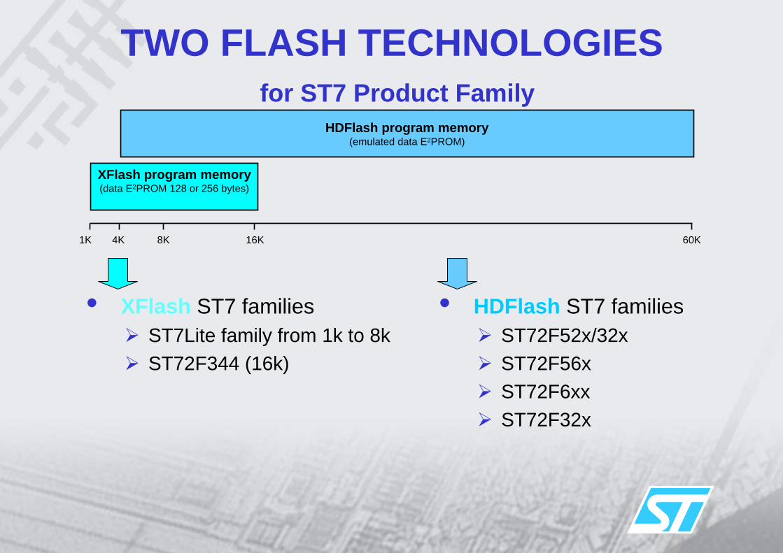
TWO FLASH TECHNOLOGIESfor ST7 Product Family
• XFlash ST7 familiesST7Lite family from 1k to 8kST72F344 (16k)
• HDFlash ST7 familiesST72F52x/32xST72F56xST72F6xxST72F32x
1K 4K 16K8K 60K
XFlash program memory(data E2PROM 128 or 256 bytes)
HDFlash program memory(emulated data E2PROM)

TWO FLASH TECHNOLOGIESfor cost vs. feature optimization
XFlashSingle voltageCycling:
10K in program memory300K in data e²prom
Programming method:Byte per byte or parallel (x32) programming withhardware control
Prog/Erase time:5ms for 1 to 32Bytes(including erasing)
Supply conditions2.4V ≤ VDD ≤ 5.5V
HDFlashDual voltageCycling:
100 in program memoryEmulated Data E²prom
Programming method:Byte per byte or parallel(x256) programming andsectorized erasing with« Embedded Commands »
Prog/Erase time:See dedicated slide
Supply conditions3.8V ≤ VDD ≤ 5.5V (dedicated low voltage version)11.4V ≤ VPP ≤ 12.6V

FLASH PROGRAMMING
• How to program:ICP: allows to PROGRAM or REPROGRAM (Xflash and HDFlash devices) the Program Memory when the micro is soldered on the application board or on an EPB socket.IAP: allows to program the whole FLASH memory exceptsector 0, when the application is running

ST7 IN-APPLICATION PROGRAMMING (IAP)
• In-Application Programming• Possible with Xflash and HDFlash• Requirements:
Standard application reset sequenceAny interface supported by the microcontroller (SPI, USB, CAN…)Always go through a RAM execution to program FLASH parts
• Capabilities: Programming of the whole FLASH memory except sector 0

ST7 IN-SITU PROGRAMING (ISP)
• What is it for ?To PROGRAM or REPROGRAM (flash devices) the Program Memory when the micro is soldered on the application board.
• Main features:Only 6 wires are used (including VDD & VSS).Do not need double voltage on the application board.Supported by ST Visual Programmer (STVP7) tools.
• Performances:~ 5 s to program 8Kbytes.

ST7 IN-SITU PROGRAMING (ISP)
1
Boot-ROM allows an executable software to be downloaded in RAM through ISPCLK & ISPDATA
Software executed in RAM programs the prog memory
Boot-ROM
RAM
ISPCLKISPDATA
RESET/ISPSELVCC/VSS
4
PROGMEMORY
I/Os
RAM
Periphs
PROGMEMORY
2
Software executed in RAM runs any applicative software with I/Osand peripherals accessIn-Situ Programming uses 6 wires only
ISPCLKISPDATA
RESET/ISPSELVCC/VSS
4

ST7 IN-CIRCUIT PROGRAMING(ICP)
• What is it for ?To PROGRAM or REPROGRAM (flash devices) the Program Memory when the micro is soldered on the application board.
• Main features:Only 4 to 7 wires are used (including VSS and clock depending theconfiguration).Do not need double voltage on the application board.Supported by the ST Visual Programmer (STVP7) tools.
• Performances:XFlash: 1.3s to program 8Kbytes.HDFlash: 640ms to program 8Kbytes
• ICP versus ISPICP based on a different protocol called ICC (In-CircuitCommunication)ICP more flexible cause the protocol adapts to the slowest part.Flash Programming and ICC Reference Manual available on Internet.
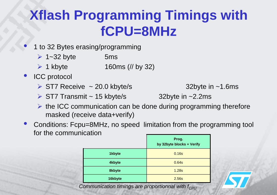
Xflash Programming Timings withfCPU=8MHz
• 1 to 32 Bytes erasing/programming1~32 byte 5ms1 kbyte 160ms (// by 32)
• ICC protocolST7 Receive ~ 20.0 kbyte/s 32byte in ~1.6msST7 Transmit ~ 15 kbyte/s 32byte in ~2.2msthe ICC communication can be done during programming thereforemasked (receive data+verify)
• Conditions: Fcpu=8MHz, no speed limitation from the programming toolfor the communication
1.28s8kbyte
2.56s16kbyte
0.64s4kbyte
0.16s1kbyte
Prog.by 32byte blocks + Verify
Communication timings are proportionnal with fCPU
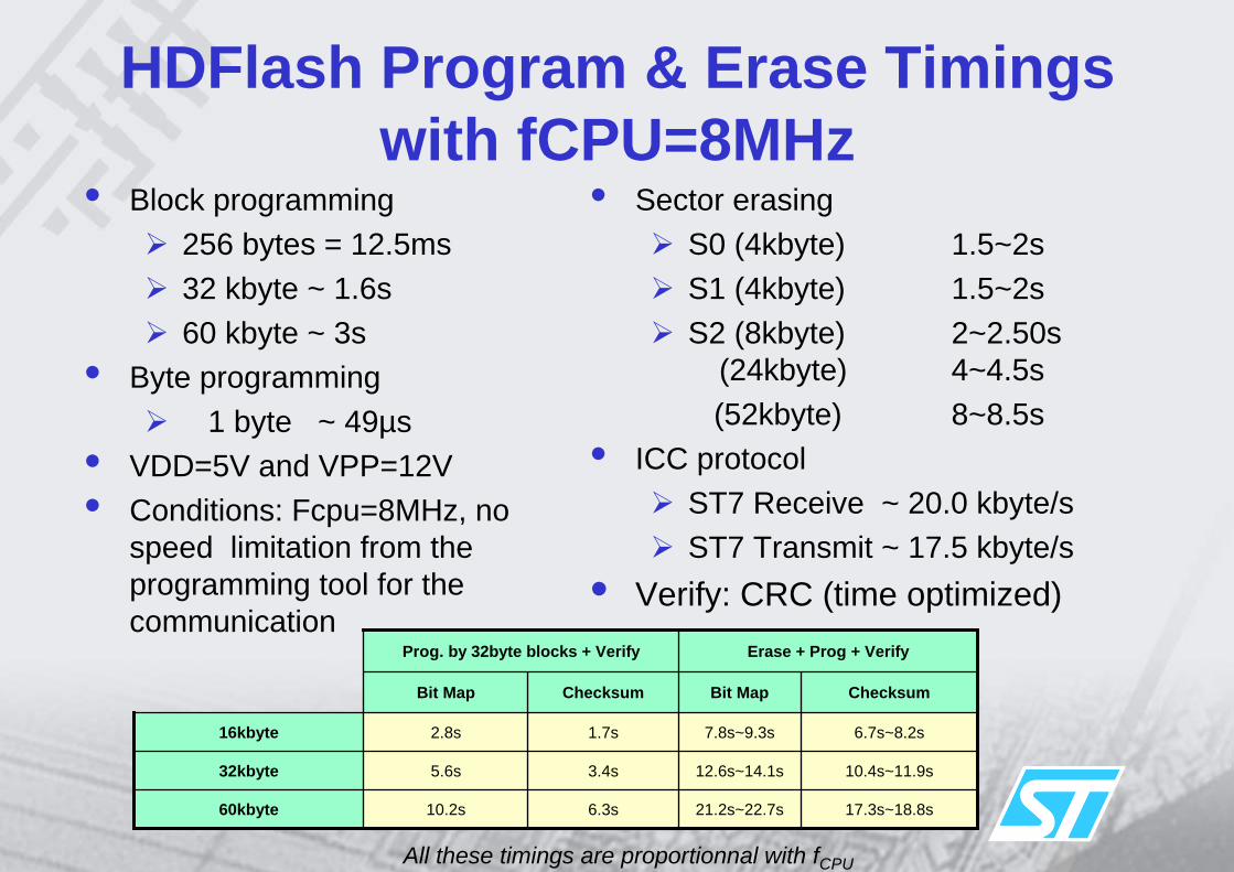
HDFlash Program & Erase Timingswith fCPU=8MHz
• Block programming256 bytes = 12.5ms 32 kbyte ~ 1.6s60 kbyte ~ 3s
• Byte programming1 byte ~ 49µs
• VDD=5V and VPP=12V• Conditions: Fcpu=8MHz, no
speed limitation from theprogramming tool for thecommunication
• Sector erasingS0 (4kbyte) 1.5~2sS1 (4kbyte) 1.5~2s S2 (8kbyte) 2~2.50s
(24kbyte) 4~4.5s(52kbyte) 8~8.5s
• ICC protocolST7 Receive ~ 20.0 kbyte/sST7 Transmit ~ 17.5 kbyte/s
• Verify: CRC (time optimized)
All these timings are proportionnal with fCPU
Erase + Prog + VerifyProg. by 32byte blocks + Verify
10.2s
5.6s
2.8s
Bit Map
6.3s
3.4s
1.7s
Checksum
21.2s~22.7s
12.6s~14.1s
7.8s~9.3s
Bit Map
17.3s~18.8s
10.4s~11.9s
6.7s~8.2s
Checksum
60kbyte
32kbyte
16kbyte

ICC MODECommunicating with ICC Protocol
Dedicated RESET sequence to enter ICC modeReal 4 pin ICC protocol
ICCCLK, ICCDATA, RESET, VSS (and VPP when needed)No speed constraint for ST7 or Controller (PC/Tester)Minimum hardware needs to connect to a PC parallel portAllow ICD emulation and ICT without any other added external HW ressourcesBidirectionnal comunication protocolOptimum command base protocol to manage ICP, ICT, ICD
Commands: Read, Write, Go, Get SP
CONTROLLER
ST7
VSSRESETICCCLKICCDATA(VPP)
ICC modeRESET sequence
ST7 receives ICC commandfrom CONTROLLER
ST7 executesICC command
ST7 executesrequested code
GO command else

SYSTEM MEMORY• Xflash :
LocationUser space(read accessible by user)
ContainsICC communication routines
• In HDFlash :Location
Paginated(no read accessible by user)
ContainsICC communication routines« Embedded commands » (Flash programmingcommands)Sector 1
Sector 0
Data E²PROM
0.5K, 1K, 2K or 4K selectable by option byte
1K to 16K
128 or 256
SYSTEM MEMORY
Sector 1
Sector 04K
0 to 52K
Sector 2
0 or 4K
SYSTEM MEMORY
NMI

PATENTED MEMORY PROTECTIONS
• Protection strategy
READOUT/W protect on Xflash
RASS (keys)(Register Access security System)
Write Protected bootloader
• Protection against
Piracy
Unexpected reprogramming
Unexpected trouble occursduring programming
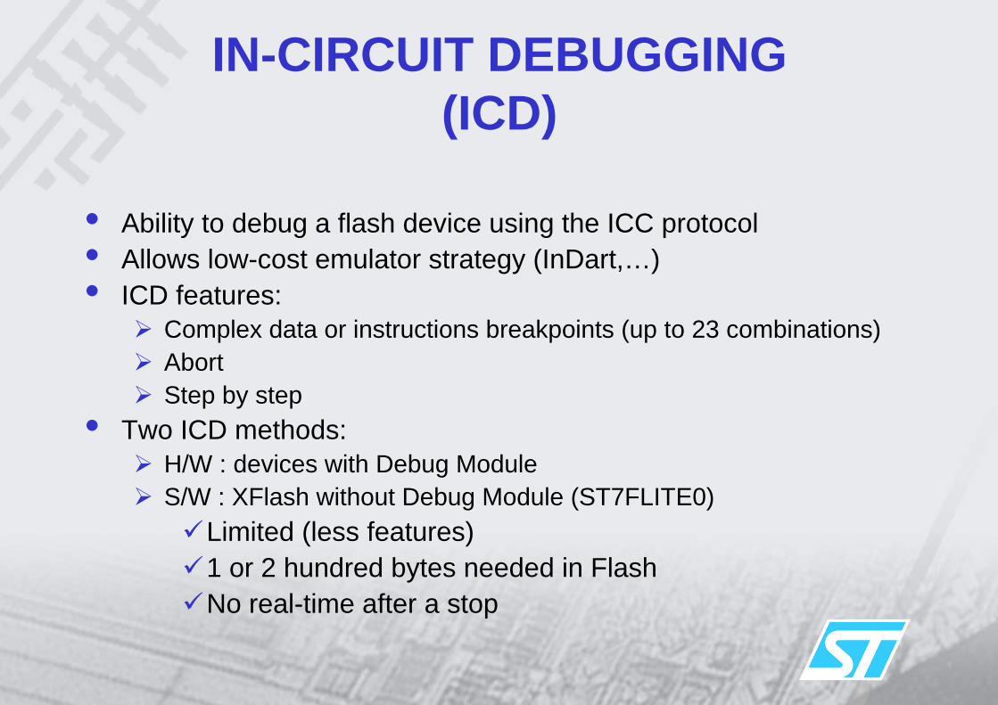
IN-CIRCUIT DEBUGGING(ICD)
• Ability to debug a flash device using the ICC protocol• Allows low-cost emulator strategy (InDart,…)• ICD features:
Complex data or instructions breakpoints (up to 23 combinations)AbortStep by step
• Two ICD methods: H/W : devices with Debug ModuleS/W : XFlash without Debug Module (ST7FLITE0)
Limited (less features)1 or 2 hundred bytes needed in FlashNo real-time after a stop

Memory & CPU registerSummary
• How Many CPU registers belong to the ST7 Core?6 registers (A, CC, X, Y, PC, SP)
• Is it possible to place and read data in ROM (programmemory)?
Yes, lookup table can be placed in ROM• Is it possible to execute code located in RAM ?
Yes, it is used in ISP and ICP modes to program the Programmemory
• Is the Stack handled automatically by the ST7 core ?Yes, the return address is loaded when a CALL is executedThe return address & the CPU registers are saved when
the interrupt process is activated

ST7 INTERRUPTSOverview
• Except for the software interrupt (TRAP Instruction), allinterrupts can be masked by setting the I BIT in CC
• When an interrupt occurs:The context is saved on the stack (CC, A, X, PC)All other interrupts are masked (the I bit is set By H/W)The interrupt vector is loaded in the Program Counter
• When return from interrupt is executed:The original context is automatically restored (CC, A, X, PC)Interrupts are enabled (I bit reset)
• Priority between interrupts is given by the interrupt address vector (Higher address = higher priority)

ST7 INTERRUPTSST72254 Interrupt mapping
CPU INTERRUPT INTERRUPTS REGISTER FLAG NAME INTERRUPT SOURCE VECTOR ADDRESSReset Reset N/A N/A - FFFEh-FFFFhTrap (instruction) Software N/A N/A I0 FFFCh-FFFDhExternal Interrupt 0 Port A N/A N/A I1 FFFAh-FFFBhExternal Interrupt 1 Port B and Port C N/A N/A I2 FFF8h-FFF9hCSS Clock Filter Interrupt CRSR CCSD I3 FFF6h-FFF7hSPI Transfer Complete SPI Status SPIF I4 FFF4h-FFF5h
Mode Fault MODFTimer A Input Capture 1 Timer A Status ICF1 I5 FFF2h-FFF3h
Output Compare 1 OCF1Input Capture 2 ICF2Output Compare 2 OCF2Timer Overflow TOF
Timer B Input Capture 1 Timer B Status ICF1 I7 FFEEh-FFEFhOutput Compare 1 OCF1Input Capture 2 ICF2Output Compare 2 OCF2Timer Overflow TOF
I2C Byte Transfer finished I2C Status BTF I12 FFE4h-FFE5hBus Error BERRSTOP Detection SSTOP
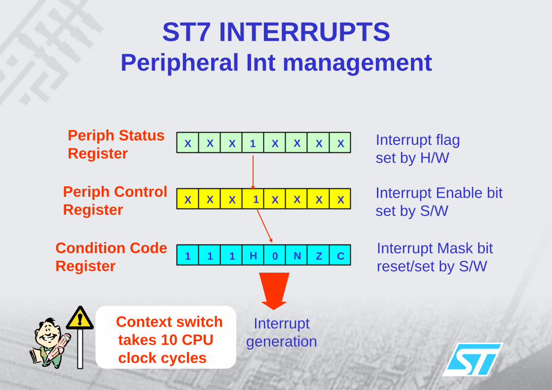
Interrupt generation
Context switch takes 10 CPU clock cycles
Periph Status Register
XX X X 1 X X X
Periph Control Register
XX X X 1 X X X
Condition Code Register
C1 1 1 H 0 N Z
Interrupt flag set by H/W
Interrupt Enable bit set by S/W
Interrupt Mask bit reset/set by S/W
ST7 INTERRUPTSPeripheral Int management
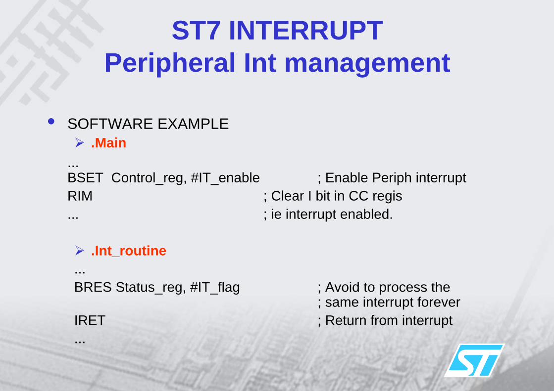
ST7 INTERRUPTPeripheral Int management
• SOFTWARE EXAMPLE.Main
...BSET Control_reg, #IT_enable ; Enable Periph interruptRIM ; Clear I bit in CC regis... ; ie interrupt enabled.
.Int_routine...BRES Status_reg, #IT_flag ; Avoid to process the
; same interrupt foreverIRET ; Return from interrupt...

Software levels allows the ST7 nested interrupt process (availability of nestedinterrupt feature is device dependant)At least one Interrupt Vector per Peripheral
ST7 Interrupt Summary
• Interrupt Vectors:• Number:• S/W Priority (Nested mode
only):• Interrupt Reaction Time:
• Automatic register pushed:
• up 16 Vectors• 16 levels hardwired• 4 levels user configurable
• 1.250µs to 2.750 µs (end of the current instruction +10 cpu cycles)
• Program counter, accumulator, CC, X
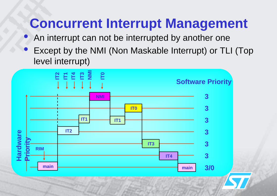
Concurrent Interrupt Management• An interrupt can not be interrupted by another one• Except by the NMI (Non Maskable Interrupt) or TLI (Top
level interrupt)
main
IT2
IT1
NMI
IT1
IT0
IT3
IT4
main
3333333/0
RIM
Har
dwar
e Pr
iorit
y
Software PriorityIT0
IT1
IT4
IT3
NM
I
IT2

Nested Interrupt
• The 4 interrupt S/W levels are set thanks to the pair of bits I0, I1.
• 1 pair of bits by interrupt vector stored in the ISPR registers• The pair of bits is copied in the CC register when the
corresponding IT is activated (software level greater than thecurrent one).
Interrupt Software Priority Level I1 I0Level 0 (main) Low 1 0Level 1 0 1Level 2 0 0Level 3 (=interrupt disable) High 1 1
to be compatiblewith previous bit I

Nested Interrupt Management• An interrupt can be interrupted by:
The NMI (Non Maskable Interrupt) or TLI (Top Level Interrupt)An interrupt request having an higher software Priority
IT1
IT4
NM
I
IT2
main
IT2
IT1
NMI
IT1
IT0
IT3
IT4
main
3321333/0
RIM
Har
dwar
e Pr
iorit
y
Software Priority
IT4
IT2
IT0
IT3

Interrupts Summary
• How many interrupt vectors can be used in the ST7 ?
Up to 16, at least one per peripheral.• Are the software interrupt levels able to be modified
during the application?Yes, in that case the interrupt routines priority can bemodified during the program execution
• What are the instructions that enable & disable theInterrupts?
RIM: Reset Interrupt Mask (I bit =0, allows the interrupts)SIM: Set interrupt Mask (I bit =1, disable the interrupts)

Multi oscillator (1)• Advanced ST7 clock system
+ Low frequency backup safety oscillator (option byte)
EXTERNAL SOURCE
OSC1 OSC2
QUARTZ/CERAMIC EXTERNAL RC
INTERNAL # 4Mhz
OSC1 OSC2
OSC1 OSC2
OSC1 OSC2
OSC1 OSC2
1% ACCURACY INTERNAL RC

• Frequency range:
1 to 2 MHz2 to 4 MHz4 to 8 MHZ8 to 16 MHz
• 1 to 14 MHz• # 1 to 8 MHz• # 250KHz and #3MHz for new
products (Xflash and HDFlash)
Multi Oscillator (2)• 4 Crystal/Ceramic Oscillators
Designed to reduce EMI & consumption
Low speedMid low speedMid high speedHigh speed
• 1 External RC Oscillator• 1 Internal RC Oscillator• 1 Internal Safe Oscillator
Oscillator selected by option byte

Main Clock Controller
Multi Oscillator
(MO)
AlternateFunction
Clock Security System (CSS)
ClockFilter
SafeOscillator
Main Clock Controller (MCC)
Clock Divider/Time Base
MCCSR Register
CORE & PERIPHERALS
fCPU or time base
fOSC
Clock divider Values:2,4,8,16,32
OSC1
OSC2
CLKOUT
Time Base Prescaler (Active Halt):32000,64000,160000,400000
PLLx2, 4 or 8(option)

RC1% Architecture• Calibration used for process, temperature
and voltage derive compensation • Expected frequency&accuracy obtained by
SW tuning and by loading RCCR registerafter each reset
LD A, $1000hLD RCCR, A
• Predefined RCCRx values stored in memoryafter calibration during ST test flow
Typical internal RC freq vs RCCR values@ 25°C
0,40,60,8
11,21,41,61,8
2 3 4 5Vdd
Freq
uenc
y (M
Hz) RCCR=00h
RCCR=64hRCCR=80hRCCR=C0hRCCR=FFh
+1%-2%T°=-40°C to 85°C, Vdd=5V
+1%-1%T°=25°C, Vdd=4.5V to 5.5V
0.5%+/-0.2%-0.5%T°=25°C, Vdd=5V
MaxTypMinConditionsRC accuracywith
RCCR=RCCR0 1MHZ
5V Range
+10%-5%T°=-40°C to 85°C, Vdd=3V
+20%-20%T°=25°C, Vdd=2.7V to 3.3V
2%+/-0.5%-2%T°=25°C, Vdd=3V
MaxTypMinConditionsRC accuracywith
RCCR=RCCR1 700KHz or 1MHz
3V Range
Typical internal RC freq with RCCR=RCCR0
0,50,60,70,80,9
11,1
2 3 4 5Vdd
Freq
uenc
y (M
Hz)
T°=-45°CT°=0°CT°=25°CT°=70°CT°=90°C
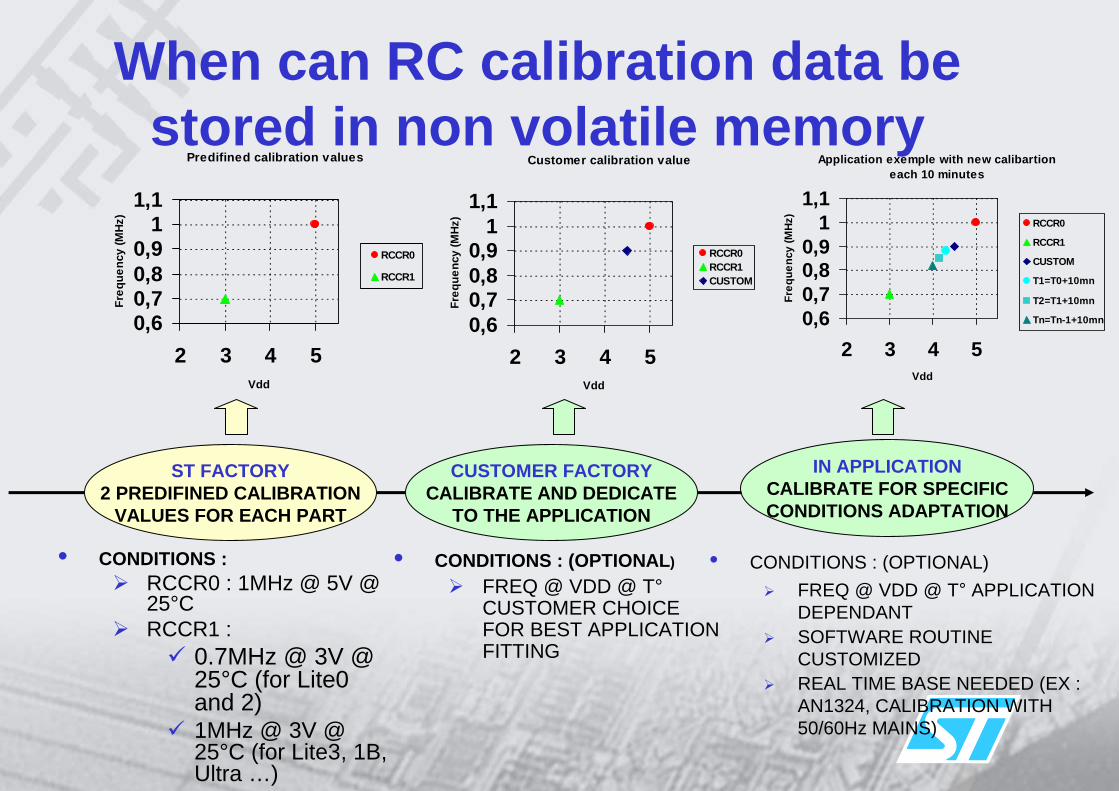
When can RC calibration data bestored in non volatile memory
• CONDITIONS :RCCR0 : 1MHz @ 5V @ 25°CRCCR1 :
0.7MHz @ 3V @ 25°C (for Lite0 and 2)1MHz @ 3V @ 25°C (for Lite3, 1B, Ultra …)
Predifined calibration values
0,60,70,80,9
11,1
2 3 4 5Vdd
Freq
uenc
y (M
Hz)
RCCR0
RCCR1
ST FACTORY2 PREDIFINED CALIBRATION
VALUES FOR EACH PART
• CONDITIONS : (OPTIONAL)
FREQ @ VDD @ T° CUSTOMER CHOICE FOR BEST APPLICATION FITTING
CUSTOMER FACTORYCALIBRATE AND DEDICATE
TO THE APPLICATION
Customer calibration value
0,60,70,80,9
11,1
2 3 4 5Vdd
Freq
uenc
y (M
Hz)
RCCR0RCCR1CUSTOM
• CONDITIONS : (OPTIONAL)FREQ @ VDD @ T° APPLICATION DEPENDANTSOFTWARE ROUTINE CUSTOMIZEDREAL TIME BASE NEEDED (EX : AN1324, CALIBRATION WITH 50/60Hz MAINS)
IN APPLICATIONCALIBRATE FOR SPECIFICCONDITIONS ADAPTATION
Application exemple with new calibartion each 10 minutes
0,60,70,80,9
11,1
2 3 4 5Vdd
Freq
uenc
y (M
Hz)
RCCR0
RCCR1
CUSTOM
T1=T0+10mn
T2=T1+10mn
Tn=Tn-1+10mn

Clock Security System
• Clock Filter Function
• Safe Oscillator
Main OscillatorClock
Internal ST7Clock
Internal ST7Clock
Main OscillatorClockSafe OscillatorClock
CSSD bit is set by H/W if one of the safety function is activated and can generate a maskable interrupt request
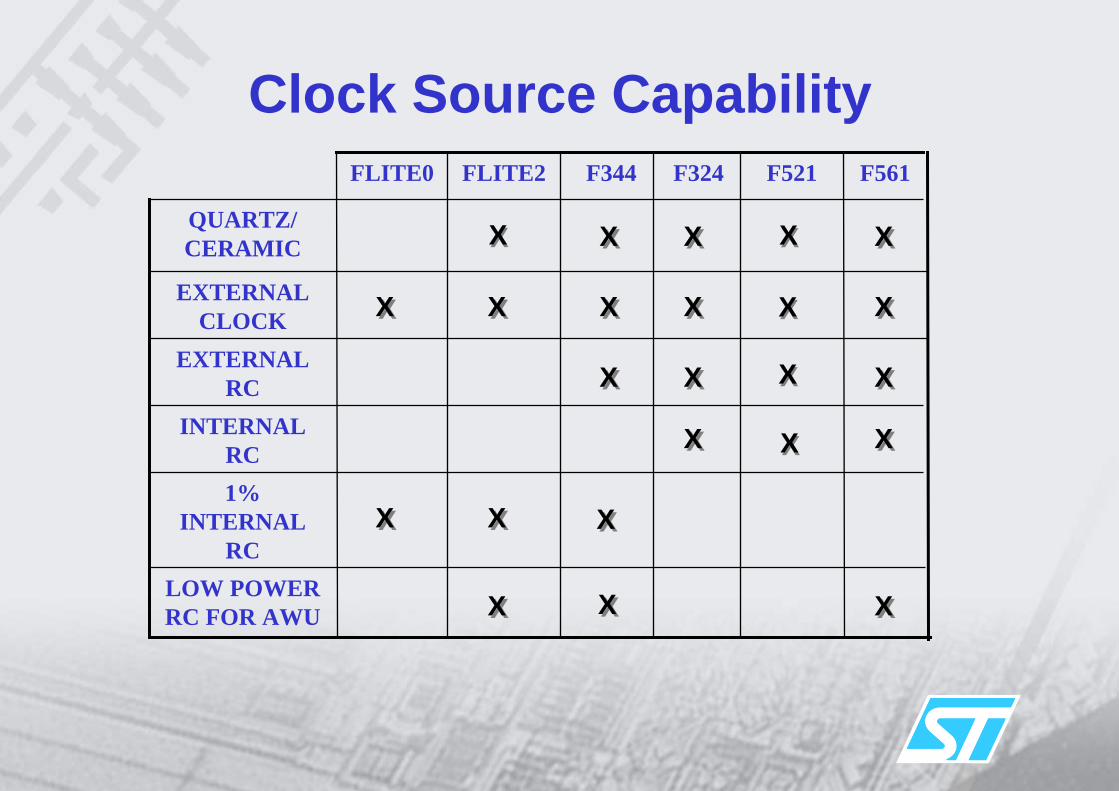
LOW POWER RC FOR AWU
EXTERNAL RC
F521FLITE0 FLITE2
1% INTERNAL
RC
INTERNAL RC
EXTERNAL CLOCK
QUARTZ/CERAMIC
F561F324F344
XX
XX
XX
XX
XX
XX
XX
XX
XX XX
XX
XX
XX
XX
XX
XX
XX
XX
Clock Source Capability
XX
XX
XX
XX
XX
XX

ST7 COREReset sources
• External reset using reset pinPurpose: allow to generate an external resetCondition: reset pin pull low
• Power supply dependent reset using LVDPurpose: ensure the MCU is in a known state whatever VccCondition: internal reset when Vcc reaches Vcc min
• Watchdog reset using the watchdog timerPurpose: guarantee the safety in case of software troubleCondition: internal reset when the WD register is not refreshed
• Illegal opcodePurpose: guarantee the safety in case of software troubleCondition: internal reset when executing an undefined prebyte or opcode

ST7 ENHANCED RESET SYSTEM• 4 Reset sources
WatchdogLow Voltage Detection (LVD)External RESET pinIllegal opcode
• Complete reset managementFlags on Reset sourcesInternal Reset externally issued to reset the whole application
From internal Watchdog Reset or Illegal Opcode: Phase # 30µsFrom internal LVD Reset: 30µs<Phase<Low voltage duration From external RESET pin: 30µs<Phase<Ext RESET pulse width
COMPLETE RESET SEQUENCE
Internal Reset4096 or 256 CPU clock
cycles
Fetch Reset Vector
Phase with RESET pin grounded
256 in the case of the clock is provided by the internal RC or by the CLKIN4096 in the case of a resonator on OSC1/OSC2

ST7 LVD GENERATION
3 Selectable levels
Activation FlagRESET pin tied to GND
VCC supply
InternalRESET
250mV hysteresis
Min working VDD
VLVDf
VLVDr
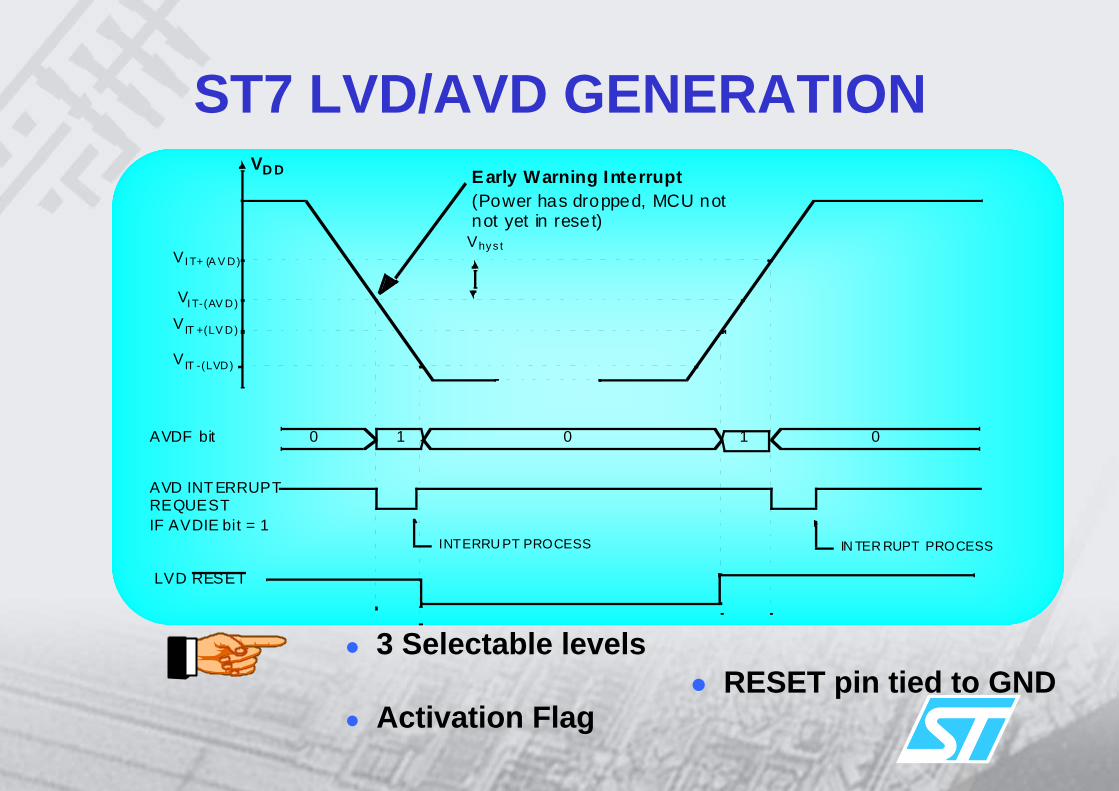
ST7 LVD/AVD GENERATION
3 Selectable levels
Activation FlagRESET pin tied to GND
VD D
VI T+ (A V D)
VI T-(AV D)
AVDF bit 0 00
IF AVDIE bit = 1
Vhys t
AVD INT ERRUPTREQUEST
INTERRU PT PROCESS IN TER RUPT PROCESS
VIT +(LV D)
VIT -(LVD)
LVD RESET
Early Warning Interrupt(Power has dropped, MCU not not yet in reset)
11

3 LVD LEVELS TO OPTIMIZE THE SAFE AREA
3.0V 3.5V 4.0V
Vsupply
Freq.
8Mhz
16Mhz
LVD highLVD med.LVD lowAbsolute working
window
Safe 16Mhz area
3.8V Reset issued
Safe 16MHzarea.
3.5V Reset issued
Safe 8Mhzarea
LVD/AVD levels are device dependant

LVD PART OF COMPLETE RESET MANAGEMENT
X1Low Voltage Reset Flag
10Watchdog Reset Flag
00External RESET pin
WDGRFLVDRFOriginal RESET source
LVD Reset ensures a
stable cleared
state of the WDGRF
when CPU starts
Vdd supply
LVDRF
LVD LVD
Software clearance
LVD
WDGRF
WDG
If LVDRF is not cleared upon
another Reset, the flag
remains SET to keep trace of
original failure.External WDG

ST7 WATCHDOGOverview (1)
• Its purpose is to detect the occurence of a software fault. It must be regularly refreshed by the program:
LD A,#$FFLD WDGCR, A ; Reload WD
• 2 different watchdogs can be selected by option bit: Hardware Watchdog:
WD automatically activated upon resetSoftware Watchdog:
It is activated by software (bit 7 = 1). Once activated, it cannot be disabled
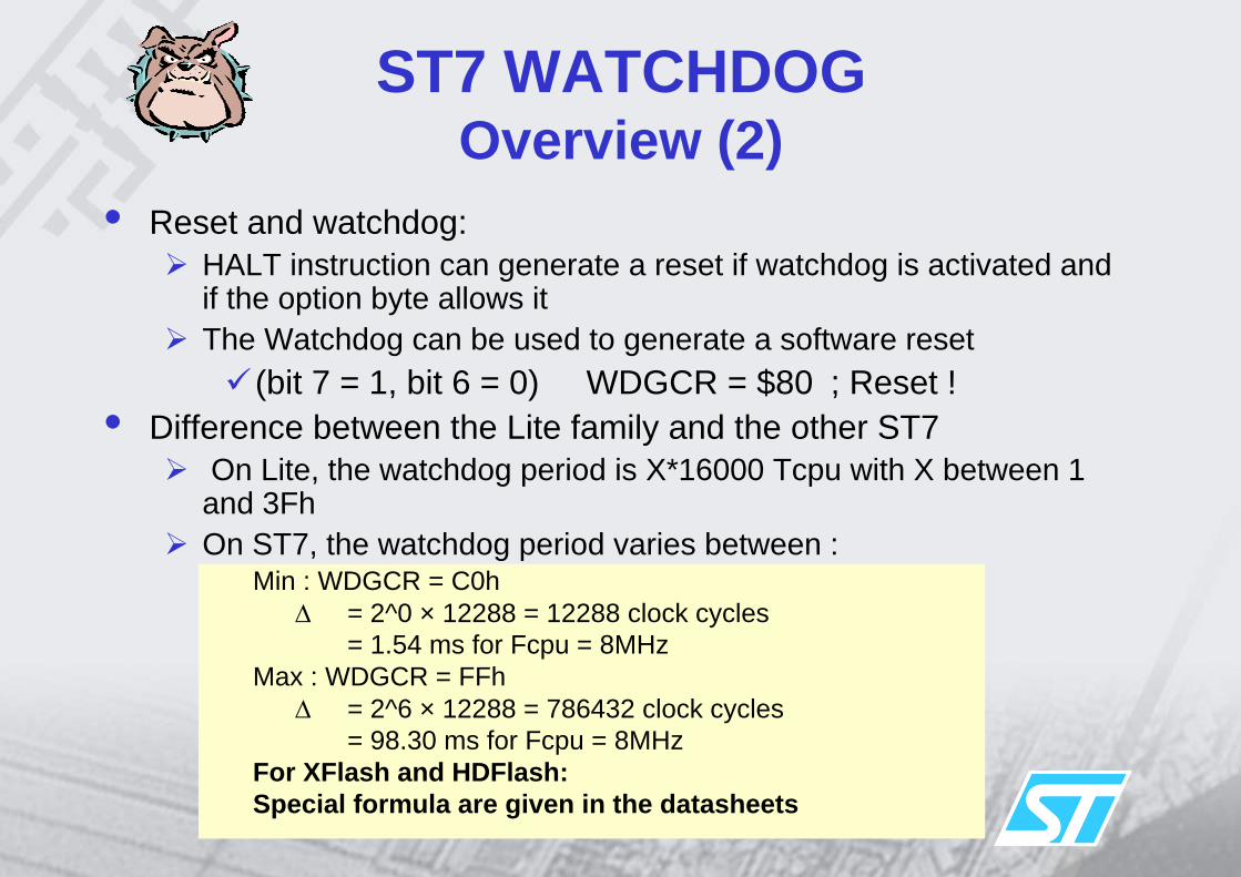
ST7 WATCHDOGOverview (2)
• Reset and watchdog:HALT instruction can generate a reset if watchdog is activated and if the option byte allows itThe Watchdog can be used to generate a software reset
(bit 7 = 1, bit 6 = 0) WDGCR = $80 ; Reset !• Difference between the Lite family and the other ST7
On Lite, the watchdog period is X*16000 Tcpu with X between 1 and 3FhOn ST7, the watchdog period varies between :
Min : WDGCR = C0h∆ = 2^0 × 12288 = 12288 clock cycles
= 1.54 ms for Fcpu = 8MHzMax : WDGCR = FFh
∆ = 2^6 × 12288 = 786432 clock cycles= 98.30 ms for Fcpu = 8MHz
For XFlash and HDFlash: Special formula are given in the datasheets

Clock & Reset systemSummary
• What are the maximun oscillator frequency and themaximun CPU frequency ?
fOSC = 16MHz & fCPU = 8 MHZ in run mode.• How many internal RC oscillator are implemented
on ST7 ?2, the first one running at 1 to 8 MHZ and the backup safety oscillator.
• What are the internal reset sources?LVD, Watchdog, Illegal opcode.
• Can these internal resets be detected externally?Yes, thanks to the reset pin that acts as an input/output pin.

ST7 CLOCK IN LOW POWER MODES
• RUN MODE: Fcpu=Fosc/2Core & periph. running except if WAIT (Core stopped) selected
• SLOW MODE: Division ratio from 4 to 32 by softwareCore & periph. running except if WAIT (Core stopped) selected
• ACTIVE HALT: Division ratio from 32000 to 400000 by softwareCore & periph. stopped but periodic wake-up through interrupts
• AUTO WAKE UP : Based on a low power internal RC allowing a periodic wake up
• HALT MODE: Oscillator stoppedCore & periph. stopped

ST7 LOW CONSUMPTION MODESOverview
• Typical ST7 consumption:HDFlash : 7 mA with fosc = 16 MHZ and VDD = 5VXFlash : 5 mA with fosc = 16 MHZ and VDD = 5V
• To reach lowest power consumptionSwitch off unused peripheralsConfigure I/Os as output low level and connect them to GNDUse the lowest oscillator frequency possibleUse the Slow mode, Wait mode or better the Halt mode

ST7 LOW CONSUMPTION MODESSlow mode
• Goal: reduce the consumption by reducing the clock speed keeping the same Oscillator frequency
• Enter by: configuring the miscellaneous register
• Causes: the CPU clock slows downThe fosc can be divided by 4, 8 ,16 or 32 rather than 2, or only 32 for small products
• Exit by: configuring the miscellaneous register

ST7 LOW CONSUMPTION MODESWait mode
• Goal: Reduce the consumption while monitoring external events
• Enter by: execution of the Wait For Interrupt instruction (WFI)• Causes: the micro is software frozen
Program execution stoppedMemory and registers remain unchangedThe oscillator still provides a clock to the peripherals
• Exit byReset (Watchdog, reset pin)Internal interrupts (timer A, timer B, A/D, SPI etc)External interrupts (I/O ports)

ST7 LOW CONSUMPTION MODESActive Halt mode
• Goal: Reduce the consumption to the lowest value while monitoring a real time clock.
• Enter by: execution of the HALT instruction while the OIE (Oscillator Interrupt Enable) bit is set.
• Causes: the micro is SW frozen, all the peripherals are stopped,only the Oscillator & the Main Oscillator Counter are running.
• Exit byExternal ResetInterrupts with exit from halt capability (External IT,..)Time Base Interrupt (32000,64000,160000,400000 *TCPU)From 2ms to 25ms with fOSC=16MHZ
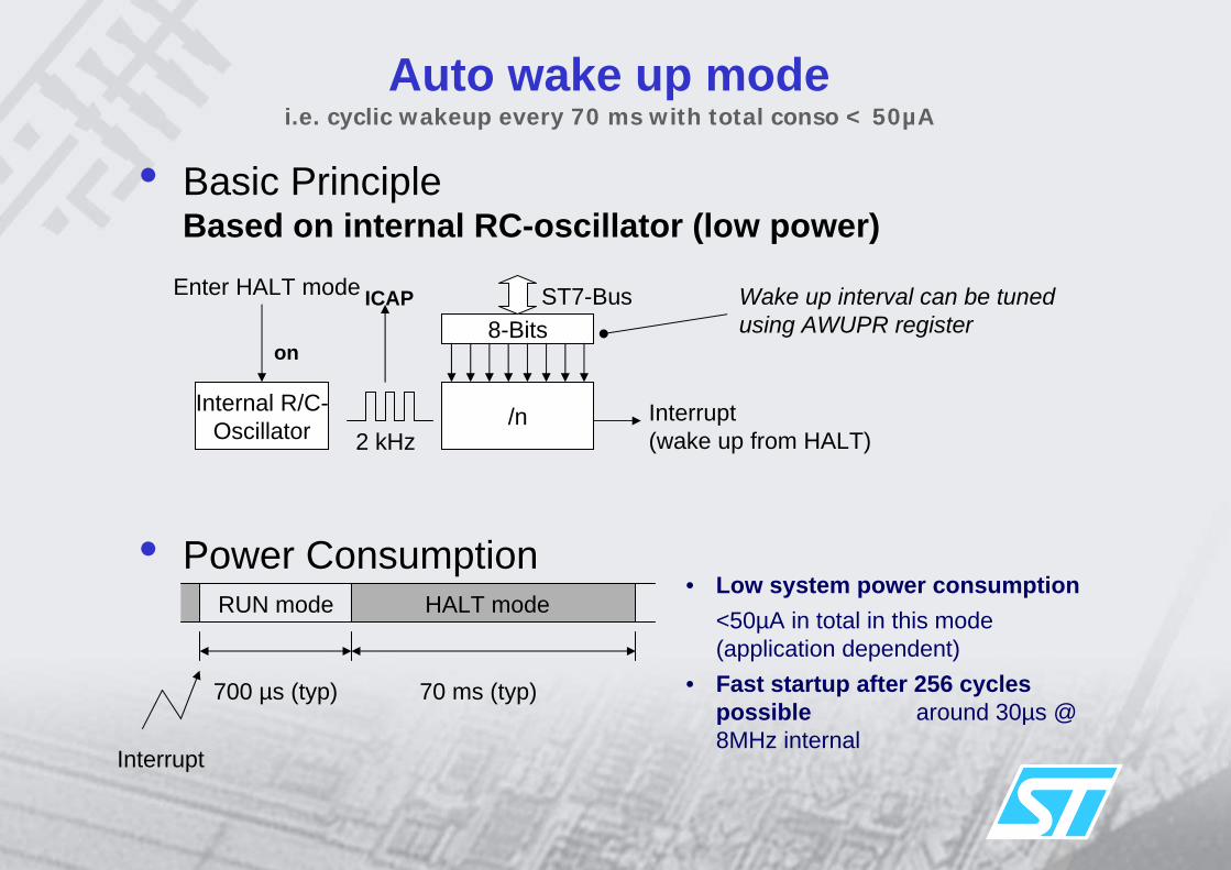
Auto wake up modei.e. cyclic wakeup every 70 ms with total conso < 50µA
• Basic PrincipleBased on internal RC-oscillator (low power)
• Power Consumption
Internal R/C-Oscillator
on
Enter HALT mode
/n
8-Bits
Interrupt(wake up from HALT)
ST7-Bus
2 kHz
Wake up interval can be tuned using AWUPR register
RUN mode HALT mode
700 µs (typ) 70 ms (typ)
Interrupt
• Low system power consumption <50µA in total in this mode (application dependent)
• Fast startup after 256 cycles possible around 30µs @ 8MHz internal
ICAP

ST7 LOW CONSUMPTION MODESHalt mode
• Goal: Reduce the consumption to the lowest value
• Enter by: execution of the HALT instruction
• Causes: the micro is SW and HW frozenProgram execution stoppedMemory and registers remain unchangedThe oscillator stopped
• Exit byExternal ResetExternal interrupts (I/O ports)

TYPICAL CONSUMPTIONS• During wait mode or HALT MODE, BIT I (INTERRUPT
BIT) of CC Register is automatically reset to enable interrupt
• Typical consumptions at Vdd=5V, Fcpu=8MHz:Auto wake up ~30µA for the ST72F561,FLITE2Active Halt ~50µA + oscillator consumption
<1µA3.5mA
1.1mA
7.1mAST72F324
<1µA<1µA<1µAHALT4.5mA3.6mA1.75mAWAIT
1.1mA0.7mA0.75mASLOW(/32)
7.1mA7.2mA4.5mARUNST72F521ST72F264ST7FLITE0

PROGRAMMING TIPSLow Consumption Modes
• After exiting from halt mode or wait mode after reset, the microwaits 256 or 4096 CPU clock cycle (STABILIZATION TIME) before being operational (clock source dependant)
• Source that allows to exit from WFI Or halt modeInternal Interrupts => Wait and Halt modesExternal Interrupts => Halt mode
• During wait mode or HALT MODE, BIT I (INTERRUPT BIT) of CC Register is automatically reset to enable interrupt