SSD1961 Application Note v1.4
28
i Amendment history Revision Description of any change Issued Effective 1.0 1 st Release Edward Cheung 23-Apr-08 1.1 Added section 3.2 for “Power Up Initialization for QVGA” Jessica Leung 30-Jul-08 1.2 Revised step 1 of section 4.3 Jessica Leung 21-Nov-08 1.3 Revised section 4 “DBC” Added section 4.2 Added section 5 “GPIO Signal)” Added 6800 interface in section 2.2 Updated command sequence in section 3 Sunny Ho 07-May-09 1.4 Removed section 3.2 for “Power Up Initialization for QVGA” Jessica Leung 25-May-09
-
Upload
fabiofurini -
Category
Documents
-
view
208 -
download
3
Transcript of SSD1961 Application Note v1.4
i
Amendment history
Revision Description of any change Issued Effective
1.0 1st Release Edward
Cheung
23-Apr-08
1.1 Added section 3.2 for “Power Up Initialization for QVGA” Jessica
Leung
30-Jul-08
1.2 Revised step 1 of section 4.3 Jessica
Leung
21-Nov-08
1.3 Revised section 4 “DBC”
Added section 4.2
Added section 5 “GPIO Signal)”
Added 6800 interface in section 2.2
Updated command sequence in section 3
Sunny Ho 07-May-09
1.4 Removed section 3.2 for “Power Up Initialization for QVGA” Jessica
Leung
25-May-09

SOLOMON SYSTECH SEMICONDUCTOR TECHNICAL DATA
This document contains information on a product under definition stage. Solomon Systech reserves the right to change or discontinue this product without notice. http://www.solomon-systech.com
SSD1961 Rev 1.0 P 1/28 Apr 2008 Copyright 2008 Solomon Systech Limited
SSD1961/2/3
Application Note for SSD1961/2/3
Solomon Systech Apr 2008 P 2/28 Rev 1. 0 SSD1961
CONTENTS
1 INTRODUCTION........................................................................................................................ 5
2 HARDWARE CONNECTION ................................................................................................... 6
2.1 HARDWARE OVERVIEWS .......................................................................................................................................6 2.2 CONNECTION TO MCU (8080 AND 6800 INTERFACE) ............................................................................................8 2.3 CONNECTION TO LCD PANEL ..............................................................................................................................11
3 PROGRAMMING EXAMPLE ................................................................................................ 13
3.1 POWER UP INITIALIZATION FOR VGA PANEL ......................................................................................................13 3.2 DEEP SLEEP MODE ..............................................................................................................................................18 3.3 WAKE UP.............................................................................................................................................................18
4 DYNAMIC BACKLIGHT CONTROL ................................................................................... 19
4.1 HARDWARE REQUIREMENT .................................................................................................................................20 4.2 PROCEDURES FOR SETTING UP DBC ....................................................................................................................21
5 GPIO MISC SIGNALS.............................................................................................................. 23
5.1 PROCEDURE TO SETUP THE GPIO ........................................................................................................................24
SSD1961 Rev 1.0 P 3/28 Apr 2008 Solomon Systech
TABLES
TABLE 2-1: CONNECTION BETWEEN SSD1961/2/3 AND MCU.............................................................................................10 TABLE 2-2: CONNECTION BETWEEN SSD1961 AND TD028TTEC1 LCD PANEL ............................................................12 TABLE 4-1: EXAMPLES OF PROGRAMMING VALUE...........................................................................................................22
Solomon Systech Apr 2008 P 4/28 Rev 1. 0 SSD1961
FIGURES
FIGURE 2-1: APPLICATION EXAMPLE OF SSD1961/2 .............................................................................................................6 FIGURE 2-2: APPLICATION EXAMPLE OF SSD1963 ................................................................................................................7 FIGURE 2-3: SSD1961/2 INTERFACES TO MCU (8080 INTERFACE) .......................................................................................8 FIGURE 2-4: SSD1963 INTERFACES TO MCU (8080 INTERFACE) ....................................................................................8 FIGURE 2-5: SSD1961/2 INTERFACES TO MCU (6800 INTERFACE) .......................................................................................9 FIGURE 2-6: SSD1963 INTERFACES TO MCU (6800 INTERFACE) ..........................................................................................9 FIGURE 2-7: TD028TTEC1 LCD PANEL INTERFACES TO SSD1961 ....................................................................................11 FIGURE 3-1 : VERTICAL TIMING OF TD028TTEC1 ..............................................................................................................14 FIGURE 3-2 : HORIZONTAL TIMING OF TD028TTEC1 .........................................................................................................14 FIGURE 4-1 : POWER COMPARISON OF DBC ........................................................................................................................19 FIGURE 4-2: DBC EXAMPLE - ORIGINAL IMAGE .............................................................................................................20 FIGURE 4-3: DBC EXAMPLE - CONSERVATIVE MODE (19% BACKLIGHT SAVED)..........................................................20 FIGURE 4-4: DBC EXAMPLE - NORMAL MODE (31% BACKLIGHT SAVED).....................................................................20 FIGURE 4-5: DBC EXAMPLE - AGGRESSIVE MODE (50% BACKLIGHT SAVED) ..............................................................20 FIGURE 4-6: EXAMPLE OF HARDWARE CONNECTION TO BENEFIT DBC ...............................................................................21
SSD1961 Rev 1.0 P 5/28 Apr 2008 Solomon Systech
1 INTRODUCTION
The display trend of mobile applications is advancing from QVGA resolution to a much higher resolution such as
HVGA, VGA, and beyond. However, interfacing between a processor to a higher resolution display panel module is not
an easy task.
One of common disconnects is the interface of the processor versus the interface of the display panel module. The
processor side usually comes with a 6800/8080-type of CPU interface which has a refresh rate of 30Hz and is often used
to interface with a smart display panel module (i.e. a full frame buffer embedded inside the display driver IC). This is
only possible if the targeted application is only for QVGA and below. When it comes to HVGA, VGA, or even higher
resolution, the frame buffer is usually too large to be integrated inside the LCD driver due to the physical limitation of
the glass that limits the aspect ratio of the LCD driver IC. Thus, the commonly found display panels at higher resolution
are a dumb panel type (i.e. without a frame buffer). The interface is usually a digital RGB interface with a refresh rate of
around 60Hz.
Even if the processor comes with an RGB interface, there could still have another potential issue – a much higher data
throughput to be supported by the processor which might impact the performance of other features. A use case scenario
of a video file playback will illustrate this idea. In this scenario, a few operations such as the operating system, file
parsing, video decoding, audio decoding, color space conversion, and resizing are working simultaneously with the LCD
controller. These operations are fighting for bus bandwidth against the LCD controller. When rotation is involved, this
situation is even worsened.
To tackle these issues, SSD1961/2/3 display controller is designed to offer a cost-effective and a simple-to-integrate
solution to the existing platforms without requiring a major overhaul of the hardware and software. In addition, an
advanced Dynamic Backlight Control (DBC) algorithm is also built-in as an extra value to significantly save the power
consumption of the LED backlight of the display module without sacrificing the display quality.
SSD1961/2/3 offers the following competitive advantages.
1. Conversion of 6800/8080-type CPU interface at 30fps or below to RGB interface at 60fps.
2. A full frame buffer is integrated. The processor can be shut down to save power while SSD1961/2/3 is still able
to refresh the display.
3. Hardware display rotation, mirroring and windowing.
4. Minimum of 2 times reduction of data throughput requirement from the processor.
5. Tearing output signal to synchronize the incoming data with the display data.
6. Dynamic Backlight Control for LED backlight power saving.
This application note serves to provide easy-to-follow instructions by illustrating the connections to SSD1961/2/3 with
the MediaTek baseband processor via the microcontroller interface and with the LCD display panel via the RGB
interface. A sample initialization code is provided for reference to show how to program SSD1961/2/3 at initial stage and
how to put SSD1961/2/3 into deep sleep mode. The Dynamic Backlight Control (DBC) feature is also explained.
Solomon Systech Apr 2008 P 6/28 Rev 1. 0 SSD1961
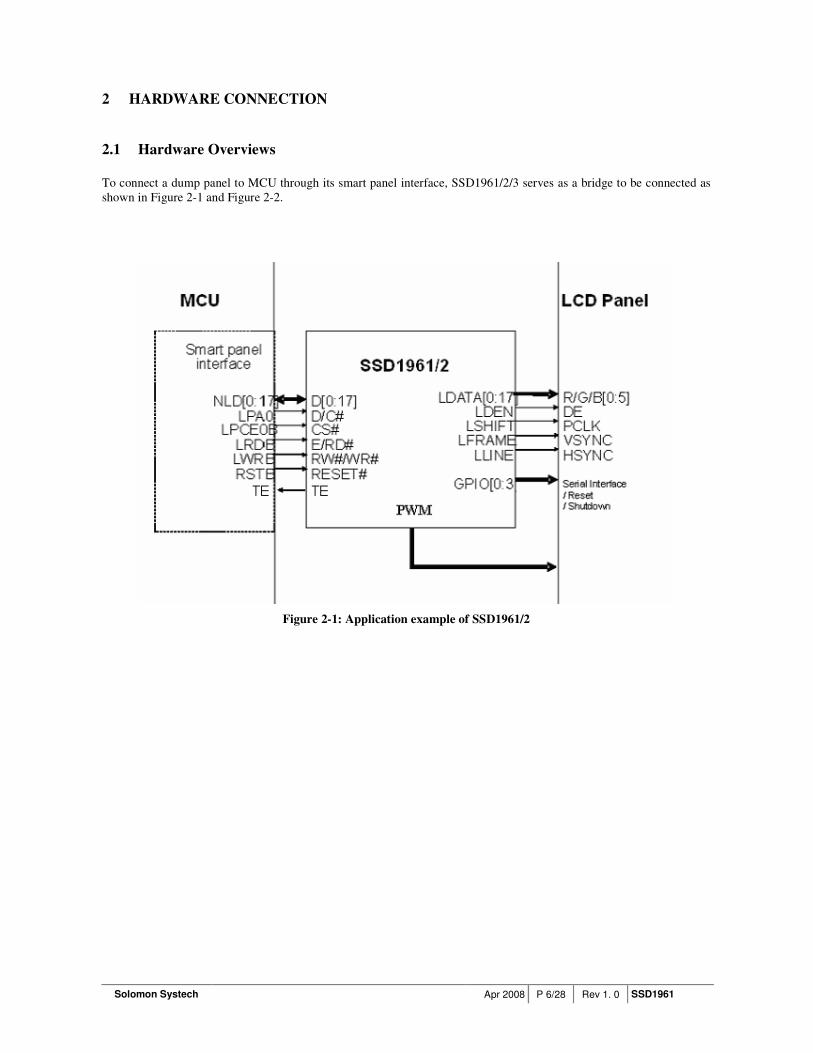
2 HARDWARE CONNECTION
2.1 Hardware Overviews
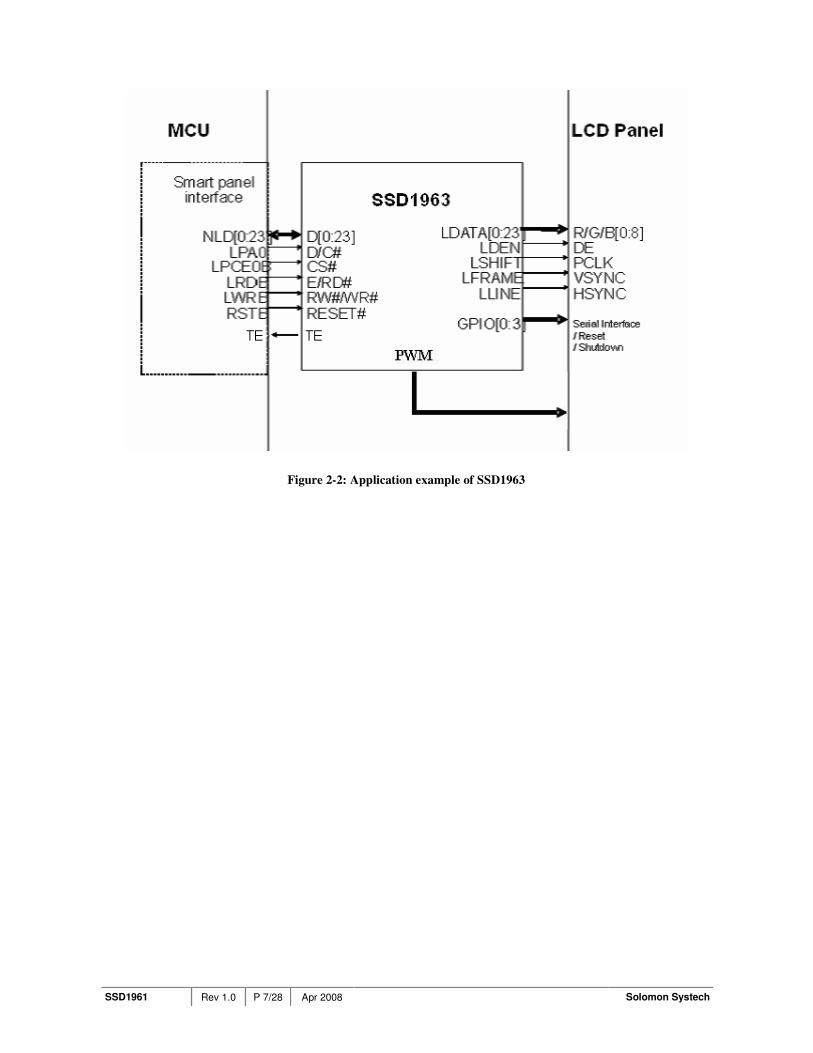
To connect a dump panel to MCU through its smart panel interface, SSD1961/2/3 serves as a bridge to be connected as
shown in Figure 2-1 and Figure 2-2.
Figure 2-1: Application example of SSD1961/2
SSD1961 Rev 1.0 P 7/28 Apr 2008 Solomon Systech
Figure 2-2: Application example of SSD1963
Solomon Systech Apr 2008 P 8/28 Rev 1. 0 SSD1961
2.2 Connection to MCU (8080 and 6800 interface)
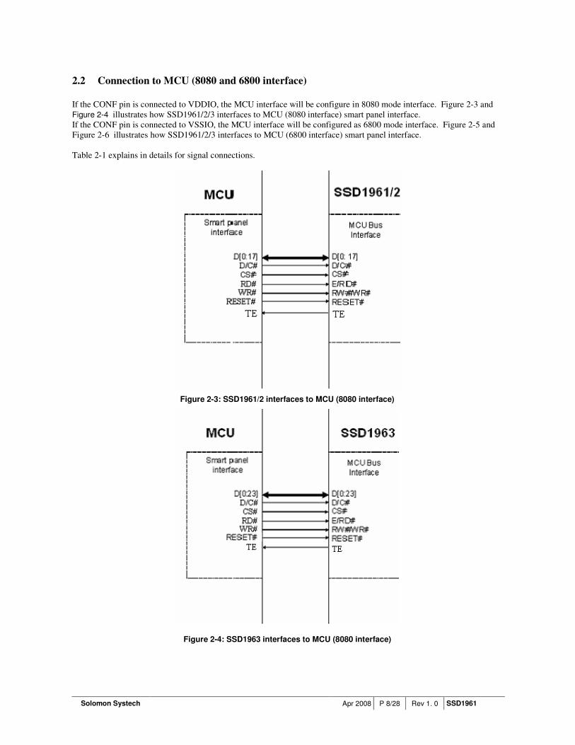
If the CONF pin is connected to VDDIO, the MCU interface will be configure in 8080 mode interface. Figure 2-3 and
Figure 2-4 illustrates how SSD1961/2/3 interfaces to MCU (8080 interface) smart panel interface.
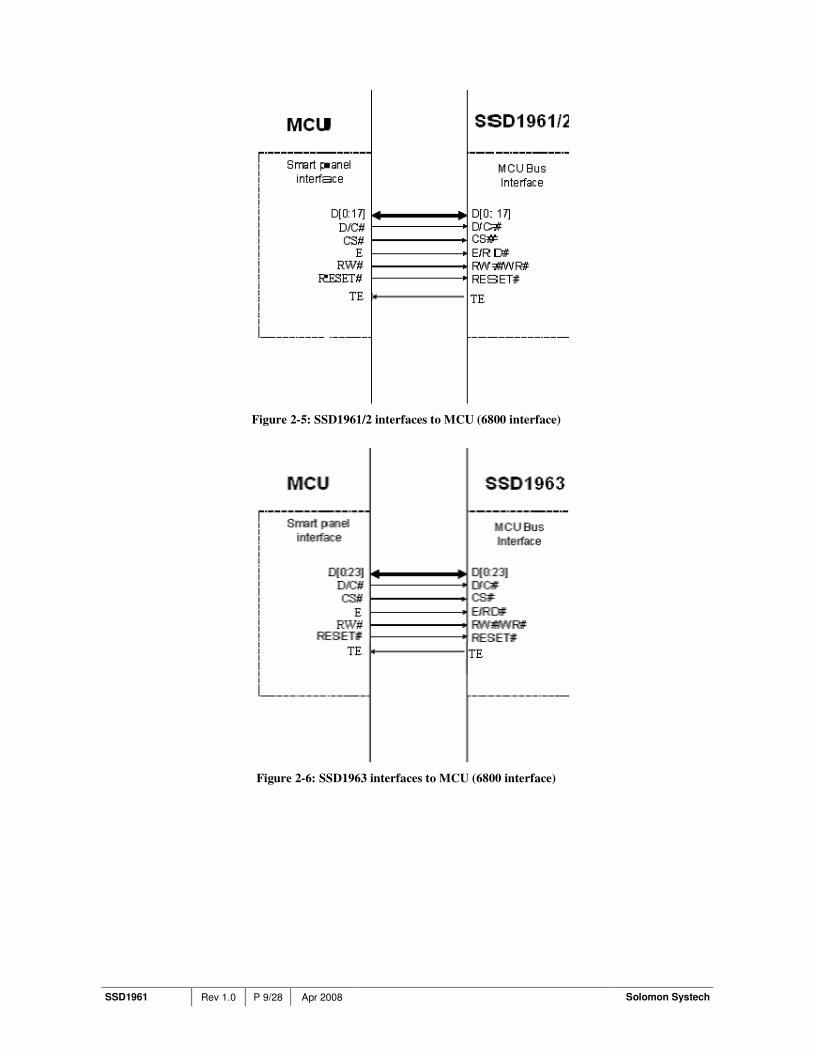
If the CONF pin is connected to VSSIO, the MCU interface will be configured as 6800 mode interface. Figure 2-5 and
Figure 2-6 illustrates how SSD1961/2/3 interfaces to MCU (6800 interface) smart panel interface.
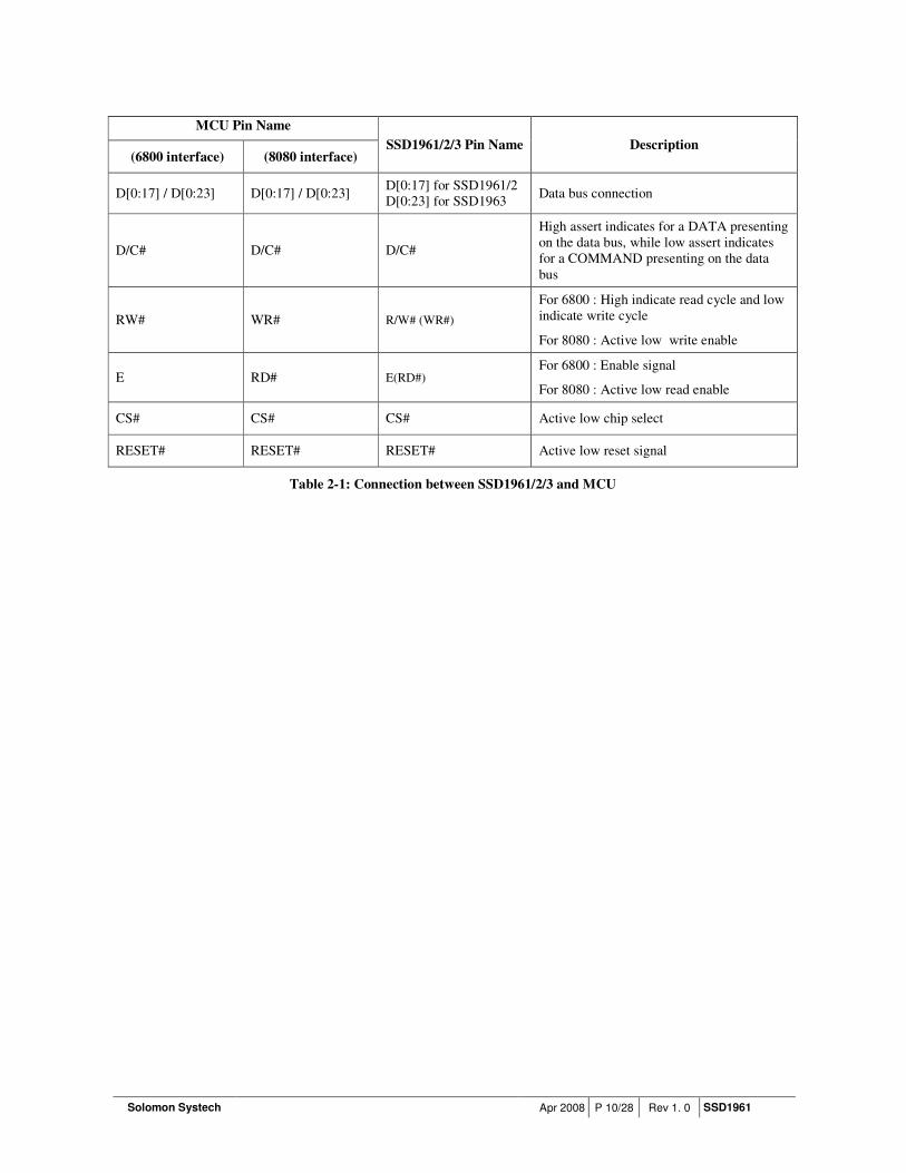
Table 2-1 explains in details for signal connections.
Figure 2-3: SSD1961/2 interfaces to MCU (8080 interface)
Figure 2-4: SSD1963 interfaces to MCU (8080 interface)
SSD1961 Rev 1.0 P 9/28 Apr 2008 Solomon Systech
Figure 2-5: SSD1961/2 interfaces to MCU (6800 interface)
Figure 2-6: SSD1963 interfaces to MCU (6800 interface)
Solomon Systech Apr 2008 P 10/28 Rev 1. 0 SSD1961
MCU Pin Name
(6800 interface) (8080 interface) SSD1961/2/3 Pin Name Description
D[0:17] / D[0:23] D[0:17] / D[0:23] D[0:17] for SSD1961/2
D[0:23] for SSD1963 Data bus connection
D/C# D/C# D/C#
High assert indicates for a DATA presenting
on the data bus, while low assert indicates
for a COMMAND presenting on the data
bus
RW# WR# R/W# (WR#)
For 6800 : High indicate read cycle and low
indicate write cycle
For 8080 : Active low write enable
E RD# E(RD#) For 6800 : Enable signal
For 8080 : Active low read enable
CS# CS# CS# Active low chip select
RESET# RESET# RESET# Active low reset signal
Table 2-1: Connection between SSD1961/2/3 and MCU
SSD1961 Rev 1.0 P 11/28 Apr 2008 Solomon Systech
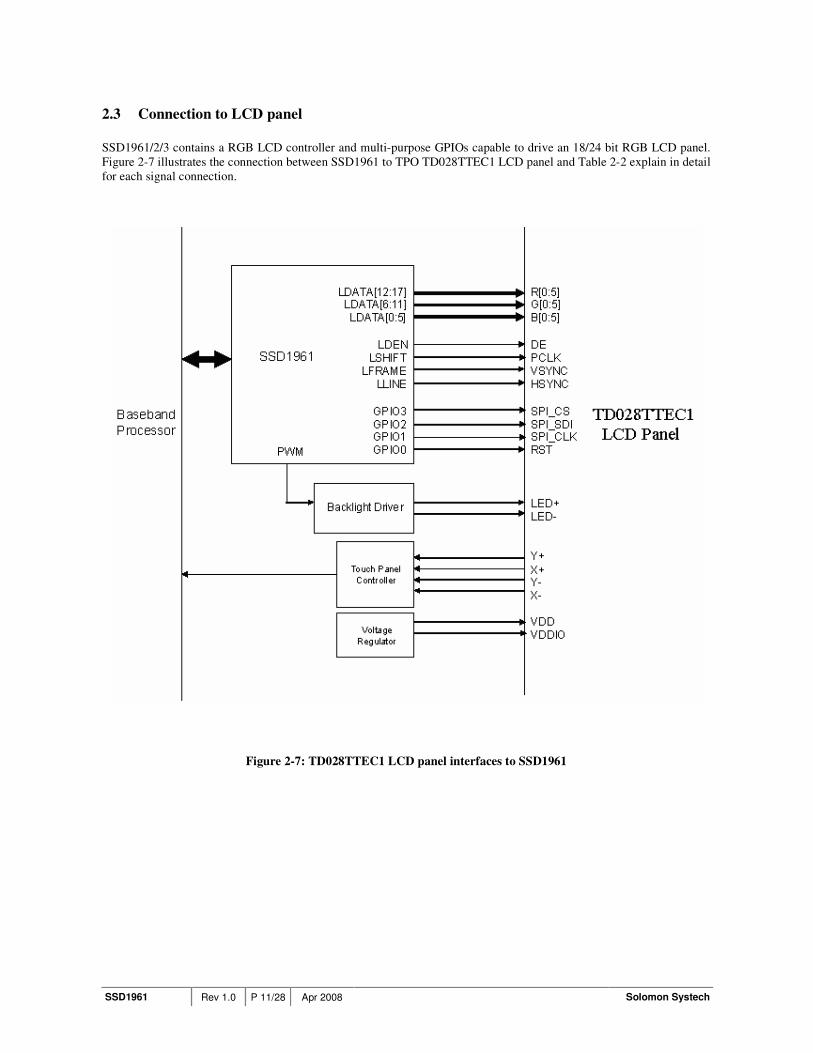
2.3 Connection to LCD panel
SSD1961/2/3 contains a RGB LCD controller and multi-purpose GPIOs capable to drive an 18/24 bit RGB LCD panel.
Figure 2-7 illustrates the connection between SSD1961 to TPO TD028TTEC1 LCD panel and Table 2-2 explain in detail
for each signal connection.
Figure 2-7: TD028TTEC1 LCD panel interfaces to SSD1961
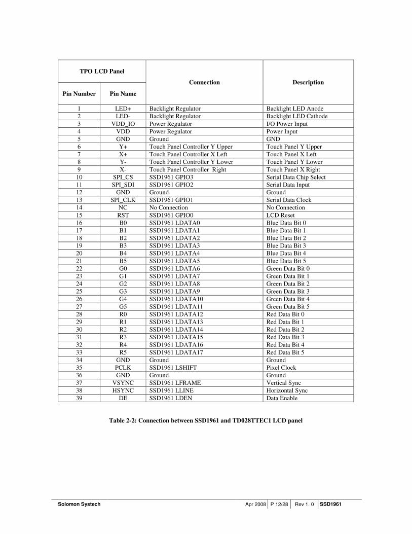
Solomon Systech Apr 2008 P 12/28 Rev 1. 0 SSD1961
TPO LCD Panel
Pin Number Pin Name
Connection Description
1 LED+ Backlight Regulator Backlight LED Anode
2 LED- Backlight Regulator Backlight LED Cathode
3 VDD_IO Power Regulator I/O Power Input
4 VDD Power Regulator Power Input
5 GND Ground GND
6 Y+ Touch Panel Controller Y Upper Touch Panel Y Upper
7 X+ Touch Panel Controller X Left Touch Panel X Left
8 Y- Touch Panel Controller Y Lower Touch Panel Y Lower
9 X- Touch Panel Controller Right Touch Panel X Right
10 SPI_CS SSD1961 GPIO3 Serial Data Chip Select
11 SPI_SDI SSD1961 GPIO2 Serial Data Input
12 GND Ground Ground
13 SPI_CLK SSD1961 GPIO1 Serial Data Clock
14 NC No Connection No Connection
15 RST SSD1961 GPIO0 LCD Reset
16 B0 SSD1961 LDATA0 Blue Data Bit 0
17 B1 SSD1961 LDATA1 Blue Data Bit 1
18 B2 SSD1961 LDATA2 Blue Data Bit 2
19 B3 SSD1961 LDATA3 Blue Data Bit 3
20 B4 SSD1961 LDATA4 Blue Data Bit 4
21 B5 SSD1961 LDATA5 Blue Data Bit 5
22 G0 SSD1961 LDATA6 Green Data Bit 0
23 G1 SSD1961 LDATA7 Green Data Bit 1
24 G2 SSD1961 LDATA8 Green Data Bit 2
25 G3 SSD1961 LDATA9 Green Data Bit 3
26 G4 SSD1961 LDATA10 Green Data Bit 4
27 G5 SSD1961 LDATA11 Green Data Bit 5
28 R0 SSD1961 LDATA12 Red Data Bit 0
29 R1 SSD1961 LDATA13 Red Data Bit 1
30 R2 SSD1961 LDATA14 Red Data Bit 2
31 R3 SSD1961 LDATA15 Red Data Bit 3
32 R4 SSD1961 LDATA16 Red Data Bit 4
33 R5 SSD1961 LDATA17 Red Data Bit 5
34 GND Ground Ground
35 PCLK SSD1961 LSHIFT Pixel Clock
36 GND Ground Ground
37 VSYNC SSD1961 LFRAME Vertical Sync
38 HSYNC SSD1961 LLINE Horizontal Sync
39 DE SSD1961 LDEN Data Enable
Table 2-2: Connection between SSD1961 and TD028TTEC1 LCD panel
SSD1961 Rev 1.0 P 13/28 Apr 2008 Solomon Systech
3 PROGRAMMING EXAMPLE
This section introduces 3 critical programming sequences for SSD1961/2/3. Section 3.1 provide an example on power up
initialization, Section 3.2 provide sample code to put SSD1961/2/3 into deep sleep mode and Section 3.3 shows how to
wake up SSD1961/2/3 from deep sleep mode.
3.1 Power Up Initialization for VGA panel
Power-up programming is required before using SSD1961/2/3 to display images. The following steps show an example
to connect SSD1961 with a 480x640 (VGA) LCD panel - TPO TD028TTEC1.
Horizontal Total, HP = 520
Horizontal Width, HDISP = 480
Horizontal Front Porch, HFP = 24
Horizontal Back Porch, HBP = 8
Horizontal Pulse Width, HS = 8
Vertical Total, VP = 648
Vertical Width, VDISP = 640
Vertical Front Porch, VFP = 4
Vertical Back Porch, VBP = 2
Vertical Pulse Width, VS = 2
Frame Rate = 65Hz
Pixel clock = 22MHz
Input clock = 10MHz
Solomon Systech Apr 2008 P 14/28 Rev 1. 0 SSD1961
Figure 3-1 : Vertical timing of TD028TTEC1
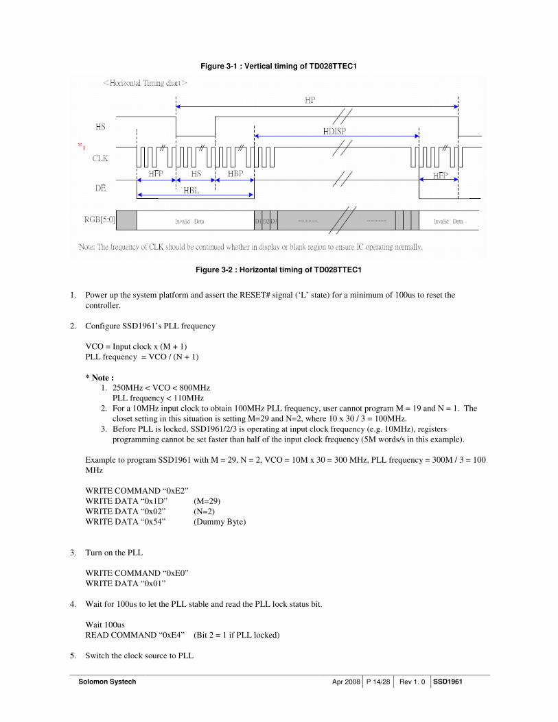
Figure 3-2 : Horizontal timing of TD028TTEC1
1. Power up the system platform and assert the RESET# signal (‘L’ state) for a minimum of 100us to reset the
controller.
2. Configure SSD1961’s PLL frequency
VCO = Input clock x (M + 1)
PLL frequency = VCO / (N + 1)
* Note :
1. 250MHz < VCO < 800MHz
PLL frequency < 110MHz
2. For a 10MHz input clock to obtain 100MHz PLL frequency, user cannot program M = 19 and N = 1. The
closet setting in this situation is setting M=29 and N=2, where 10 x 30 / 3 = 100MHz.
3. Before PLL is locked, SSD1961/2/3 is operating at input clock frequency (e.g. 10MHz), registers
programming cannot be set faster than half of the input clock frequency (5M words/s in this example).
Example to program SSD1961 with M = 29, N = 2, VCO = 10M x 30 = 300 MHz, PLL frequency = 300M / 3 = 100
MHz
WRITE COMMAND “0xE2”
WRITE DATA “0x1D” (M=29)
WRITE DATA “0x02” (N=2)
WRITE DATA “0x54” (Dummy Byte)
3. Turn on the PLL
WRITE COMMAND “0xE0”
WRITE DATA “0x01”
4. Wait for 100us to let the PLL stable and read the PLL lock status bit.
Wait 100us
READ COMMAND “0xE4” (Bit 2 = 1 if PLL locked)
5. Switch the clock source to PLL
SSD1961 Rev 1.0 P 15/28 Apr 2008 Solomon Systech
WRITE COMMAND “0xE0”
WRITE DATA “0x03”
6. Software Reset
WRITE COMMAND “0x01”
7. Configure the dot clock frequency
For example,
22MHz = 100MHz * (LCDC_FPR+1) / 220
LCDC_FPR = 230686=0x3851D
WRITE COMMAND “0xE6”
WRITE DATA “0x03”
WRITE DATA “0x85”
WRITE DATA “0x1D”
8. Configure the LCD panel
a. Set the panel size to 480 x 640 and polarity of LSHIFT, LLINE and LFRAME to active low
WRITE COMMAND “0xB0”
WRITE DATA “0x0C” // 18bit panel, disable dithering, LSHIFT: Data latch in rising edge,
LLINE and LFRAME: active low
WRITE DATA “0x00” // TFT type
WRITE DATA “0x01” // Horizontal Width: 480 - 1 = 0x1DF
WRITE DATA “0xDF”
WRITE DATA “0x02” // Vertical Width : 640 -1 = 0x27F
WRITE DATA “0x7F”
WRITE DATA “0x00” // dummy for TFT
b. Set the horizontal period
WRITE COMMAND “0xB4” // Horizontal Display Period
WRITE DATA “0x02” // HT: horizontal total period (display + non-display) – 1 = 520-1 =
WRITE DATA “0x07” 519 =0x0207
WRITE DATA “0x00” // HPS: Horizontal Sync Pulse Start Position = Horizontal Pulse
WRITE DATA “0x10” Width + Horizontal Back Porch = 16 = 0x10
WRITE DATA “0x07” // HPW: Horizontal Sync Pulse Width - 1=8-1=7
WRITE DATA “0x00” // LPS: Horizontal Display Period Start Position = 0x0000
WRITE DATA “0x00”
WRITE DATA “0x00” // LPSPP: Horizontal Sync Pulse Subpixel Start Position(for serial
TFT interface). Dummy value for TFT interface.
c. Set the vertical period
WRITE COMMAND “0xB6” // Vertical Display Period
WRITE DATA “0x02” // VT: Vertical Total (display + non-display) Period – 1
WRITE DATA “0x87” =647=0x287
WRITE DATA “0x00” // VPS: Vertical Sync Pulse Start Position =
WRITE DATA “0x04” Vertical Pulse Width + Vertical Back Porch = 2+2=4
WRITE DATA “0x01” //VPW: Vertical Sync Pulse Width – 1 =1
WRITE DATA “0x00” //FPS: Vertical Display Period Start Position = 0
WRITE DATA “0x00”
9. Set the back light control PWM clock frequency
Solomon Systech Apr 2008 P 16/28 Rev 1. 0 SSD1961
PWM signal frequency = PLL clock / (256 * (PWMF[7:0] + 1)) / 256
WRITE COMMAND “0xBE” // PWM configuration
WRITE DATA “0x08” // set PWM signal frequency to 170Hz when PLL frequency is 100MHz
WRITE DATA “0x80” // PWM duty cycle (50%)
WRITE DATA “0x01” // 0x09 = enable DBC, 0x01 = disable DBC
10. Configure the GPIO
WRITE COMMAND “0xB8”
WRITE DATA “0x0E” // Config GPIO3-1 as output, GPIO0 as input
WRITE DATA “0x01” // shutdown control not used
WRITE COMMAND “0xBA”
WRITE DATA “0x0E” // Set GPIO3-1 as high
11. Turn on the display
WRITE COMMAND “0x29” // display on
12. Config the frame buffer
a. Setup the frame buffer vertical addressing range to “1 to 480”
WRITE COMMAND “0x2A” // set column address
WRITE DATA “0x00” // SC: 0 = 0x0000
WRITE DATA “0x00”
WRITE DATA “0x01” // EC: 480 -1 = 479 = 0x01DF
WRITE DATA “0xDF”
b. Setup the frame buffer horizontal address range to “1 to 640”
WRITE COMMAND “0x2B” // set page address
WRITE DATA “0x00” //SP: 0 = 0x0000
WRITE DATA “0x00”
WRITE DATA “0x02” // EP: 640 -1 = 639 = 0x027F
WRITE DATA “0x7F”
13. Setup the addressing mode to rotate mode
* Note : In this example, the screen is assumed to be presented as landscape mode. Skip this step for portrait mode.
WRITE COMMAND “0x36” // set address_mode
WRITE DATA “0x60” // bit 5 is column page swap (rotate mode), bit 6 is optional.
14. Setup the MCU interface for 18-bit data write
WRITE COMMAND “0xF0” // mcu interface config
WRITE DATA “0x04” // 18 bit interface
*.Note : The un-used data bus will be driven to ground by SSD1961, so don’t connect the un-used data bus to
MCU..
15. Start to write the data to frame buffer with command “write_memory_start”
WRITE COMMAND “0x2C” // write memory start
SSD1961 Rev 1.0 P 17/28 Apr 2008 Solomon Systech
WRITE DATA “...... “ // 640 x 480 display data

Solomon Systech Apr 2008 P 18/28 Rev 1. 0 SSD1961
3.2 Deep Sleep Mode
SSD1961/2/3 supports deep sleep mode for power saving. To push SSD1961/2/3 entering deep sleep mode, the
following statements are required to be programmed to SSD1961/2/3 registers:
1. Write command to enter sleep mode
WRITE COMMAND “0x10”
External LCD signals and all internal clocks would be stopped.
2. Write command set deep sleep
WRITE COMMAND “0xE5”
PLL would be stopped.
3. Stop CLKIN (reference input clock) for power consumption
3.3 Wake Up
1. To wake up SSD1961/2/3, do two dummy reads to SSD1961/2/3.
2. Wait for 100us to let the PLL stable and read the PLL lock status bit.
Wait 100us
READ COMMAND “0xE4” (Bit 2 = 1 if PLL locked)
3. Turn on the display by writing:
WRITE COMMAND “0x11”
4. Wait for 5ms
SSD1961 Rev 1.0 P 19/28 Apr 2008 Solomon Systech
4 DYNAMIC BACKLIGHT CONTROL
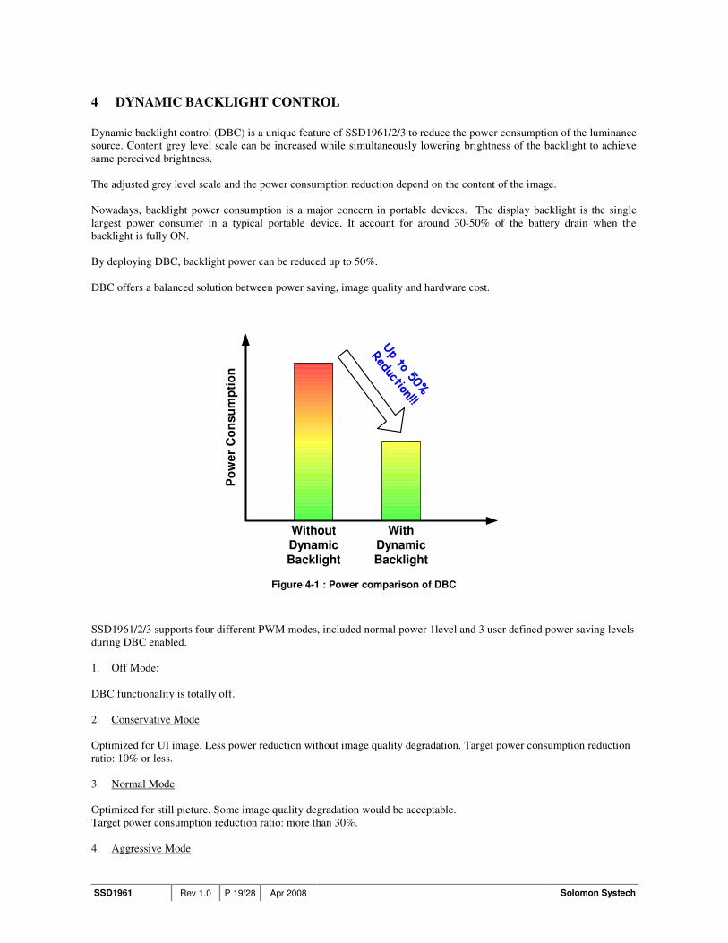
Dynamic backlight control (DBC) is a unique feature of SSD1961/2/3 to reduce the power consumption of the luminance
source. Content grey level scale can be increased while simultaneously lowering brightness of the backlight to achieve
same perceived brightness.
The adjusted grey level scale and the power consumption reduction depend on the content of the image.
Nowadays, backlight power consumption is a major concern in portable devices. The display backlight is the single
largest power consumer in a typical portable device. It account for around 30-50% of the battery drain when the
backlight is fully ON.
By deploying DBC, backlight power can be reduced up to 50%.
DBC offers a balanced solution between power saving, image quality and hardware cost.
Po
we
r C
on
su
mp
tio
n
WithoutDynamicBacklight
WithDynamicBacklight
Up to 50%
Reduction!!!
Figure 4-1 : Power comparison of DBC
SSD1961/2/3 supports four different PWM modes, included normal power 1level and 3 user defined power saving levels
during DBC enabled.
1. Off Mode:
DBC functionality is totally off.
2. Conservative Mode
Optimized for UI image. Less power reduction without image quality degradation. Target power consumption reduction
ratio: 10% or less.
3. Normal Mode
Optimized for still picture. Some image quality degradation would be acceptable.
Target power consumption reduction ratio: more than 30%.
4. Aggressive Mode
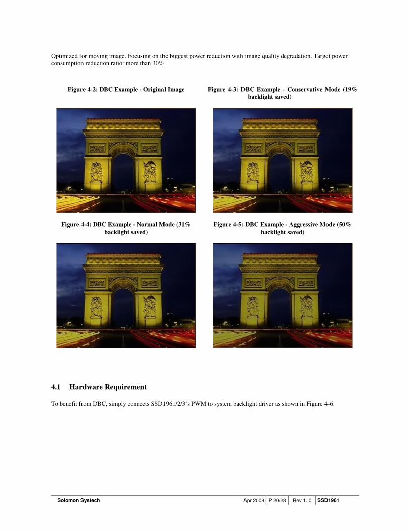
Solomon Systech Apr 2008 P 20/28 Rev 1. 0 SSD1961
Optimized for moving image. Focusing on the biggest power reduction with image quality degradation. Target power
consumption reduction ratio: more than 30%
Figure 4-2: DBC Example - Original Image Figure 4-3: DBC Example - Conservative Mode (19%
backlight saved)
Figure 4-4: DBC Example - Normal Mode (31%
backlight saved)
Figure 4-5: DBC Example - Aggressive Mode (50%
backlight saved)
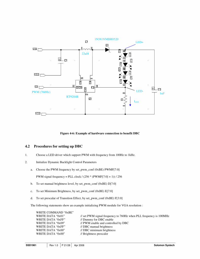
4.1 Hardware Requirement
To benefit from DBC, simply connects SSD1961/2/3’s PWM to system backlight driver as shown in Figure 4-6.
SSD1961 Rev 1.0 P 21/28 Apr 2008 Solomon Systech
Figure 4-6: Example of hardware connection to benefit DBC
4.2 Procedures for setting up DBC
1. Choose a LED driver which support PWM with frequency from 100Hz to 1kHz.
2. Initialize Dynamic Backlight Control Parameters
a. Choose the PWM frequency by set_pwm_conf (0xBE) PWMF[7:0]
PWM signal frequency = PLL clock / (256 * (PWMF[7:0] + 1)) / 256
b. To set manual brightness level, by set_pwm_conf (0xBE) D[7:0]
c. To set Minimum Brightness, by set_pwm_conf (0xBE) E[7:0]
d. To set prescalar of Transition Effect, by set_pwm_conf (0xBE) F[3:0]
The following statements show an example initializing PWM module for VGA resolution :
WRITE COMMAND “0xBE”
WRITE DATA “0x01” // set PWM signal frequency to 760Hz when PLL frequency is 100MHz
WRITE DATA “0xFF” // Dummy for DBC enable
WRITE DATA “0x09” // PWM enable and controlled by DBC
WRITE DATA “0xFF” // DBC manual brightness
WRITE DATA “0x00” // DBC minimum brightness
WRITE DATA “0x00” // Brightness prescaler
PWM (760Hz)
LED+
LED- 1uF
22uH
1N5819/MBR0520
RT9284B
ILED
Solomon Systech Apr 2008 P 22/28 Rev 1. 0 SSD1961
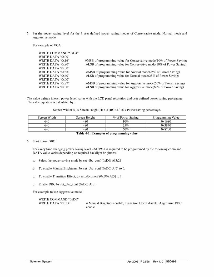
5. Set the power saving level for the 3 user defined power saving modes of Conservative mode, Normal mode and
Aggressive mode.
For example of VGA :
WRITE COMMAND “0xD4”
WRITE DATA “0x00”
WRITE DATA “0x16” //MSB of programming value for Conservative mode(10% of Power Saving)
WRITE DATA “0x80” //LSB of programming value for Conservative mode(10% of Power Saving)
WRITE DATA “0x00”
WRITE DATA “0x38” //MSB of programming value for Normal mode(25% of Power Saving)
WRITE DATA “0x40” //LSB of programming value for Normal mode(25% of Power Saving)
WRITE DATA “0x00”
WRITE DATA “0x87” //MSB of programming value for Aggressive mode(60% of Power Saving)
WRITE DATA “0x00” //LSB of programming value for Aggressive mode(60% of Power Saving)
The value written in each power level varies with the LCD panel resolution and user defined power saving percentage.
The value equation is calculated by:
Screen Width(W) x Screen Height(H) x 3 (RGB) / 16 x Power saving percentage.
Screen Width Screen Height % of Power Saving Programming Value
640 480 10% 0x1680
640 480 25% 0x3840
640 480 60% 0x8700
Table 4-1: Examples of programming value
6. Start to use DBC
For every time changing power saving level, SSD1961 is required to be programmed by the following command.
DATA value varies depending on required backlight brightness.
a. Select the power saving mode by set_dbc_conf (0xD0) A[3:2]
b. To enable Manual Brightness, by set_dbc_conf (0xD0) A[6] to 0.
c. To enable Transition Effect, by set_dbc_conf (0xD0) A[5] to 1.
d. Enable DBC by set_dbc_conf (0xD0) A[0].
For example to use Aggressive mode :
WRITE COMMAND “0xD0”
WRITE DATA “0x0D” // Manual Brightness enable, Transition Effect disable, Aggressive DBC
enable
SSD1961 Rev 1.0 P 23/28 Apr 2008 Solomon Systech
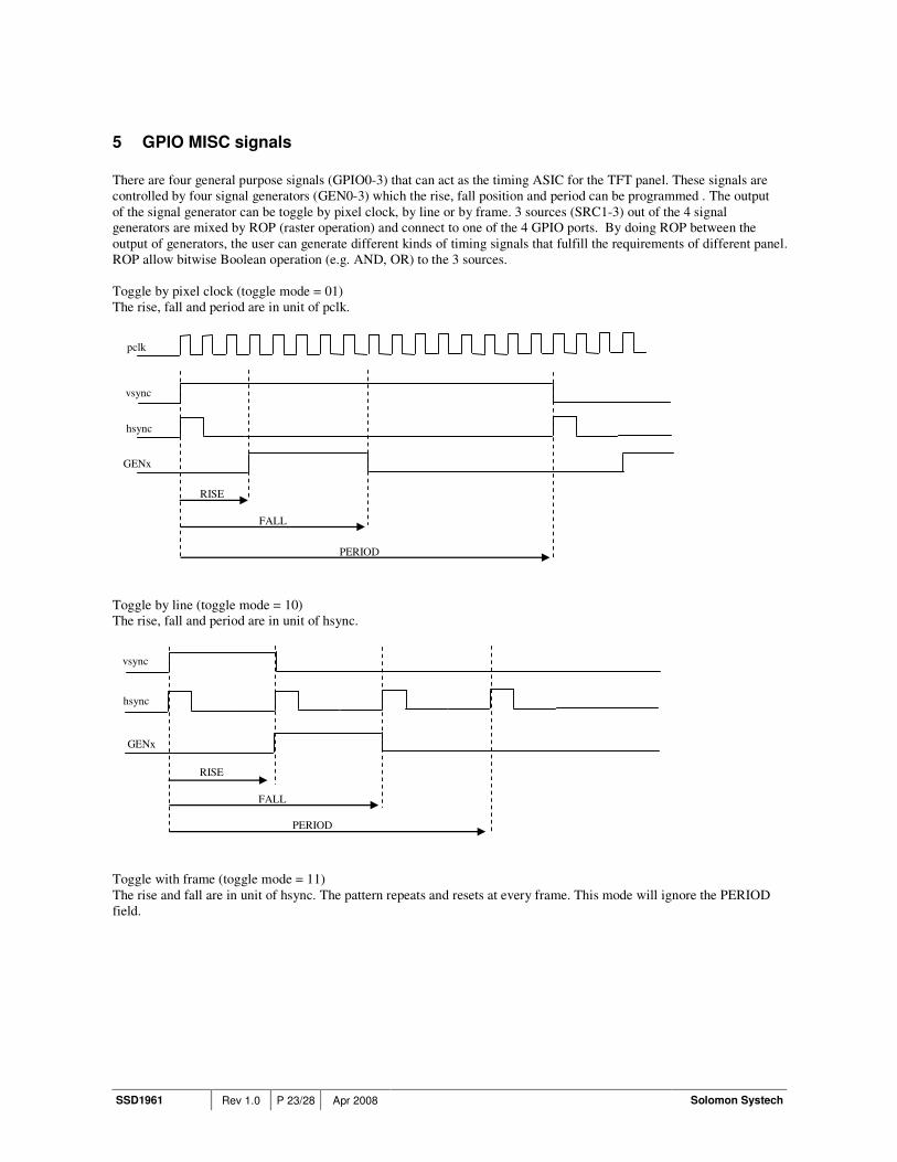
5 GPIO MISC signals
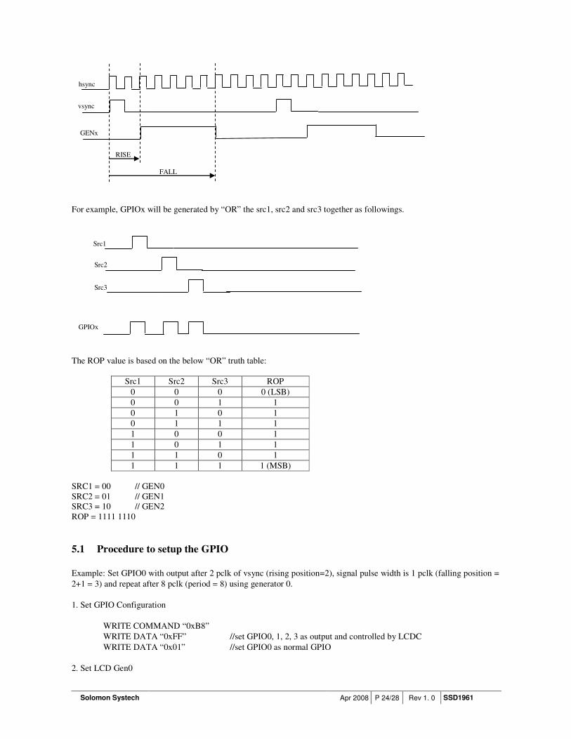
There are four general purpose signals (GPIO0-3) that can act as the timing ASIC for the TFT panel. These signals are
controlled by four signal generators (GEN0-3) which the rise, fall position and period can be programmed . The output
of the signal generator can be toggle by pixel clock, by line or by frame. 3 sources (SRC1-3) out of the 4 signal
generators are mixed by ROP (raster operation) and connect to one of the 4 GPIO ports. By doing ROP between the
output of generators, the user can generate different kinds of timing signals that fulfill the requirements of different panel.
ROP allow bitwise Boolean operation (e.g. AND, OR) to the 3 sources.
Toggle by pixel clock (toggle mode = 01)
The rise, fall and period are in unit of pclk.
RISE
FALL
L
PERIOD
vsync
hsync
GENx
pclk
Toggle by line (toggle mode = 10)
The rise, fall and period are in unit of hsync.
RISE
FALL
L
PERIOD
vsync
hsync
GENx
Toggle with frame (toggle mode = 11)
The rise and fall are in unit of hsync. The pattern repeats and resets at every frame. This mode will ignore the PERIOD
field.
Solomon Systech Apr 2008 P 24/28 Rev 1. 0 SSD1961
vsync
GENx
RISE
FALL
L
hsync
For example, GPIOx will be generated by “OR” the src1, src2 and src3 together as followings.
Src1
Src2
Src3
GPIOx
The ROP value is based on the below “OR” truth table:
Src1 Src2 Src3 ROP
0 0 0 0 (LSB)
0 0 1 1
0 1 0 1
0 1 1 1
1 0 0 1
1 0 1 1
1 1 0 1
1 1 1 1 (MSB)
SRC1 = 00 // GEN0
SRC2 = 01 // GEN1
SRC3 = 10 // GEN2
ROP = 1111 1110
5.1 Procedure to setup the GPIO
Example: Set GPIO0 with output after 2 pclk of vsync (rising position=2), signal pulse width is 1 pclk (falling position =
2+1 = 3) and repeat after 8 pclk (period = 8) using generator 0.
1. Set GPIO Configuration
WRITE COMMAND “0xB8”
WRITE DATA “0xFF” //set GPIO0, 1, 2, 3 as output and controlled by LCDC
WRITE DATA “0x01” //set GPIO0 as normal GPIO
2. Set LCD Gen0
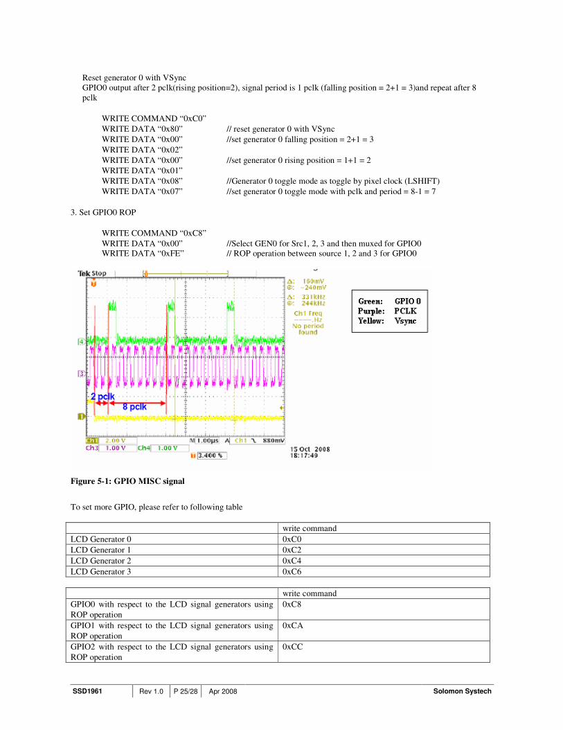
SSD1961 Rev 1.0 P 25/28 Apr 2008 Solomon Systech
Reset generator 0 with VSync
GPIO0 output after 2 pclk(rising position=2), signal period is 1 pclk (falling position = 2+1 = 3)and repeat after 8
pclk
WRITE COMMAND “0xC0”
WRITE DATA “0x80” // reset generator 0 with VSync
WRITE DATA “0x00” //set generator 0 falling position = 2+1 = 3
WRITE DATA “0x02”
WRITE DATA “0x00” //set generator 0 rising position = 1+1 = 2
WRITE DATA “0x01”
WRITE DATA “0x08” //Generator 0 toggle mode as toggle by pixel clock (LSHIFT)
WRITE DATA “0x07” //set generator 0 toggle mode with pclk and period = 8-1 = 7
3. Set GPIO0 ROP
WRITE COMMAND “0xC8”
WRITE DATA “0x00” //Select GEN0 for Src1, 2, 3 and then muxed for GPIO0
WRITE DATA “0xFE” // ROP operation between source 1, 2 and 3 for GPIO0
Figure 5-1: GPIO MISC signal
To set more GPIO, please refer to following table
write command
LCD Generator 0 0xC0
LCD Generator 1 0xC2
LCD Generator 2 0xC4
LCD Generator 3 0xC6
write command
GPIO0 with respect to the LCD signal generators using
ROP operation
0xC8
GPIO1 with respect to the LCD signal generators using
ROP operation
0xCA
GPIO2 with respect to the LCD signal generators using
ROP operation
0xCC
Solomon Systech Apr 2008 P 26/28 Rev 1. 0 SSD1961
GPIO3 with respect to the LCD signal generators using
ROP operation
0xCE
Solomon Systech reserves the right to make changes without notice to any products herein. Solomon Systech makes no warranty,
representation or guarantee regarding the suitability of its products for any particular purpose, nor does Solomon Systech assume any
liability arising out of the application or use of any product or circuit, and specifically disclaims any, and all, liability, including without
limitation consequential or incidental damages. “Typical” parameters can and do vary in different applications. All operating parameters, including “Typical” must be validated for each customer application by the customer’s technical experts. Solomon Systech does not con-
vey any license under its patent rights nor the rights of others. Solomon Systech products are not designed, intended, or authorized for use
as components in systems intended for surgical implant into the body, or other applications intended to support or sustain life, or for any
other application in which the failure of the Solomon Systech product could create a situation where personal injury or death may occur.
Should Buyer purchase or use Solomon Systech products for any such unintended or unauthorized application, Buyer shall indemnify and
hold Solomon Systech and its offices, employees, subsidiaries, affiliates, and distributors harmless against all claims, costs, damages, and expenses, and reasonable attorney fees arising out of, directly or indirectly, any claim of personal injury or death associated with such
unintended or unauthorized use, even if such claim alleges that Solomon Systech was negligent regarding the design or manufacture of the
part.
All Solomon Systech Products complied with six (6) hazardous substances limitation requirement per European Union (EU) “Restriction of
Hazardous Substance (RoHS) Directive (2002/95/EC)” and China standard “电子信息产品污染控制标识要求 (SJ/T11364-2006)” with
control Marking Symbol . Hazardous Substances test report is available upon requested.
http://www.solomon-systech.com