SSD1327 - Génération Robots · Solomon Systech Dec 2008 P 2/68 Rev 1.1 SSD1327 ... P.55 Updated...
68
SOLOMON SYSTECH SEMICONDUCTOR TECHNICAL DATA This document contains information on a new product. Specifications and information herein are subject to change without notice. http://www.solomon-systech.com SSD1327 Rev 1.1 P 1/68 Dec 2008 Copyright © 2008 Solomon Systech Limited Advance Information 128 x 128, 16 Gray Scale Dot Matrix OLED/PLED Segment/Common Driver with Controller SSD1327
Transcript of SSD1327 - Génération Robots · Solomon Systech Dec 2008 P 2/68 Rev 1.1 SSD1327 ... P.55 Updated...

SOLOMON SYSTECH SEMICONDUCTOR TECHNICAL DATA
This document contains information on a new product. Specifications and information herein are subject to change without notice. http://www.solomon-systech.com SSD1327 Rev 1.1 P 1/68 Dec 2008 Copyright © 2008 Solomon Systech Limited
Advance Information
128 x 128, 16 Gray Scale Dot Matrix OLED/PLED Segment/Common Driver with Controller
SSD1327

Solomon Systech Dec 2008 P 2/68 Rev 1.1 SSD1327
Appendix: IC Revision history of SSD1327 Specification
Version Change Items Effective Date
0.10 1st release
30-May-08
0.20 P.17 Added TR[6:0] on pin description section P.37, 38 Added notes for commands B1h and B8h on command table P.54 Updated the DC characteristics table P.55 Updated the AC characteristics table
04-Sep-08
0.30
P.8, 10 Revise die thickness tolerance from ±25um to ±15um P.11, 12 Revised the typo of LVSS to VLSS on the table of SSD1327Z Bump Die Pad Coordinates P.15, 39, 50 Added command D5h and corresponding information on the command table and related section P.49 Added display on and display off sequences P.62 Added notes (4) and (5) on the application example of SSD1327Z
21-Nov-08
1.0 Change to Advance information P.7 Added title “VCI and VDD range” for Table 2-1 P.35 Updated section 8.10 VDD regulator P.37 Revised command table of “Function Selection A (ABh)” P.49 Revised description of section 10.1.10 Function Selection A (ABh) P.49, 50 Revised section 10.1.11 Set display ON/OFF P.59 – 63 Updated the condition of AC characteristics from (VDD - VSS = 2.4V to 2.6V, VCI = 3.3V) to (VCI - VSS = 1.65V to 3.5V) on Table 13-2 to Table13-6
09-Dec-08
1.1 P.38 Added a note for command B6h on command table P.51 Revised the description of command B6h
23-Dec-08

SSD1327 Rev 1.1 P 3/68 Dec 2008 Solomon Systech
CONTENT
1 GENERAL DESCRIPTION ....................................................................................................7
2 FEATURES................................................................................................................................7
3 ORDERING INFORMATION ................................................................................................8
4 BLOCK DIAGRAM..................................................................................................................9
5 DIE PAD FLOORPLAN.........................................................................................................10
6 PIN ARRANGEMENT...........................................................................................................13
7 PIN DESCRIPTIONS .............................................................................................................15
8 FUNCTIONAL BLOCK DESCRIPTIONS..........................................................................18 8.1 MCU INTERFACE SELECTION...............................................................................................................................18
8.1.1 MCU Parallel 6800-series Interface......................................................................................................18 8.1.2 MCU Parallel 8080-series Interface......................................................................................................19 8.1.3 MCU Serial Interface (4-wire SPI) ........................................................................................................20 8.1.4 MCU Serial Interface (3-wire SPI) ........................................................................................................21 8.1.5 MCU I2C Interface .................................................................................................................................22
8.1.5.1 I2C-bus Write data..................................................................................................................23 8.1.5.2 Write mode for I2C..................................................................................................................23
8.2 SEGMENT DRIVERS/COMMON DRIVERS...............................................................................................................25 8.3 OSCILLATOR CIRCUIT AND DISPLAY TIME GENERATOR......................................................................................28 8.4 COMMAND DECODER AND COMMAND INTERFACE..............................................................................................29 8.5 RESET CIRCUIT ....................................................................................................................................................29 8.6 SEG/COM DRIVING BLOCK................................................................................................................................29 8.7 GRAPHIC DISPLAY DATA RAM (GDDRAM)......................................................................................................30 8.8 GRAY SCALE DECODER .......................................................................................................................................33 8.9 POWER ON AND OFF SEQUENCE .........................................................................................................................34 8.10 VDD REGULATOR .................................................................................................................................................35
9 COMMAND TABLE ..............................................................................................................36 9.1 DATA READ / WRITE ...........................................................................................................................................41
10 COMMAND DESCRIPTIONS..............................................................................................42 10.1 FUNDAMENTAL COMMAND DESCRIPTION ............................................................................................................42
10.1.1 Set Column Address (15h)...................................................................................................................42 10.1.2 Set Row Address (75h) ........................................................................................................................42 10.1.3 Set Contrast Current (81h) .................................................................................................................43 10.1.4 NOP (84h ~ 86h).................................................................................................................................43 10.1.5 Set Re-map (A0h) ................................................................................................................................43 10.1.6 Set Display Start Line (A1h) ...............................................................................................................46 10.1.7 Set Display Offset (A2h)......................................................................................................................47 10.1.8 Set Display Mode (A4h ~ A7h)............................................................................................................48 10.1.9 Set Multiplex Ratio (A8h)....................................................................................................................49 10.1.10 Function selection A (ABh) .................................................................................................................49 10.1.11 Set Display ON/OFF (AEh / AFh) ......................................................................................................49 10.1.12 Set Phase Length (B1h).......................................................................................................................50 10.1.13 NOP (B2h) ..........................................................................................................................................50 10.1.14 Set Front Clock Divider / Oscillator Frequency (B3h).......................................................................50 10.1.15 Set GPIO (B5h) ...................................................................................................................................50 10.1.16 Set Second Pre-charge period (B6h)...................................................................................................51 10.1.17 Set Gray Scale Table (B8h).................................................................................................................51 10.1.18 Select Default Linear Gray Scale Table (B9h)....................................................................................51 10.1.19 NOP (BBh) ..........................................................................................................................................51 10.1.20 Set Pre-charge voltage (BCh) .............................................................................................................51

Solomon Systech Dec 2008 P 4/68 Rev 1.1 SSD1327
10.1.21 Set VCOMH Voltage (BEh).....................................................................................................................51 10.1.22 Function selection B (D5h) .................................................................................................................52 10.1.23 Set Command Lock (FDh)...................................................................................................................52
10.2 GRAPHIC ACCELERATION COMMAND DESCRIPTION.............................................................................................53 10.2.1 Horizontal Scroll Setup (26h/27h) ......................................................................................................53 10.2.2 Deactivate Scroll (2Eh).......................................................................................................................54 10.2.3 Activate Scroll (2Fh)...........................................................................................................................54
11 MAXIMUM RATINGS ..........................................................................................................55
12 DC CHARACTERISTICS .....................................................................................................56
13 AC CHARACTERISTICS .....................................................................................................57
14 APPLICATION EXAMPLES................................................................................................63
15 PACKAGE INFORMATION ................................................................................................65 15.1 SSD1327Z DIE TRAY INFORMATION...................................................................................................................65 15.2 SSD1327UR1 DETAIL DIMENSION.......................................................................................................................67
SSD1327 Rev 1.1 P 5/68 Dec 2008 Solomon Systech
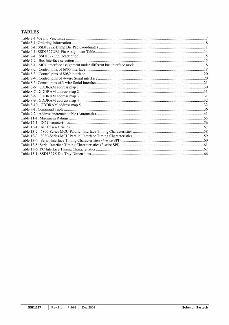
TABLES Table 2-1 VCI and VDD range ................................................................................................................................................7 Table 3-1: Ordering Information ..........................................................................................................................................8 Table 5-1: SSD1327Z Bump Die Pad Coordinates ............................................................................................................11 Table 6-1: SSD1327UR1 Pin Assignment Table................................................................................................................14 Table 7-1 : SSD1327 Pin Description.................................................................................................................................15 Table 7-2 : Bus Interface selection .....................................................................................................................................15 Table 8-1 : MCU interface assignment under different bus interface mode .......................................................................18 Table 8-2 : Control pins of 6800 interface..........................................................................................................................18 Table 8-3 : Control pins of 8080 interface..........................................................................................................................20 Table 8-4 : Control pins of 4-wire Serial interface .............................................................................................................20 Table 8-5: Control pins of 3-wire Serial interface ..............................................................................................................21 Table 8-6 : GDDRAM address map 1 ................................................................................................................................30 Table 8-7 : GDDRAM address map 2 ................................................................................................................................31 Table 8-8 : GDDRAM address map 3 ................................................................................................................................31 Table 8-9 : GDDRAM address map 4 ................................................................................................................................32 Table 8-10 : GDDRAM address map 5 ..............................................................................................................................32 Table 9-1: Command Table ................................................................................................................................................36 Table 9-2 : Address increment table (Automatic)...............................................................................................................41 Table 11-1: Maximum Ratings ...........................................................................................................................................55 Table 12-1 : DC Characteristics..........................................................................................................................................56 Table 13-1 : AC Characteristics..........................................................................................................................................57 Table 13-2 : 6800-Series MCU Parallel Interface Timing Characteristics .........................................................................58 Table 13-3 : 8080-Series MCU Parallel Interface Timing Characteristics .........................................................................59 Table 13-4 : Serial Interface Timing Characteristics (4-wire SPI) .....................................................................................60 Table 13-5: Serial Interface Timing Characteristics (3-wire SPI) ......................................................................................61 Table 13-6: I2C Interface Timing Characteristics ...............................................................................................................62 Table 15-1: SSD1327Z Die Tray Dimensions....................................................................................................................66
Solomon Systech Dec 2008 P 6/68 Rev 1.1 SSD1327
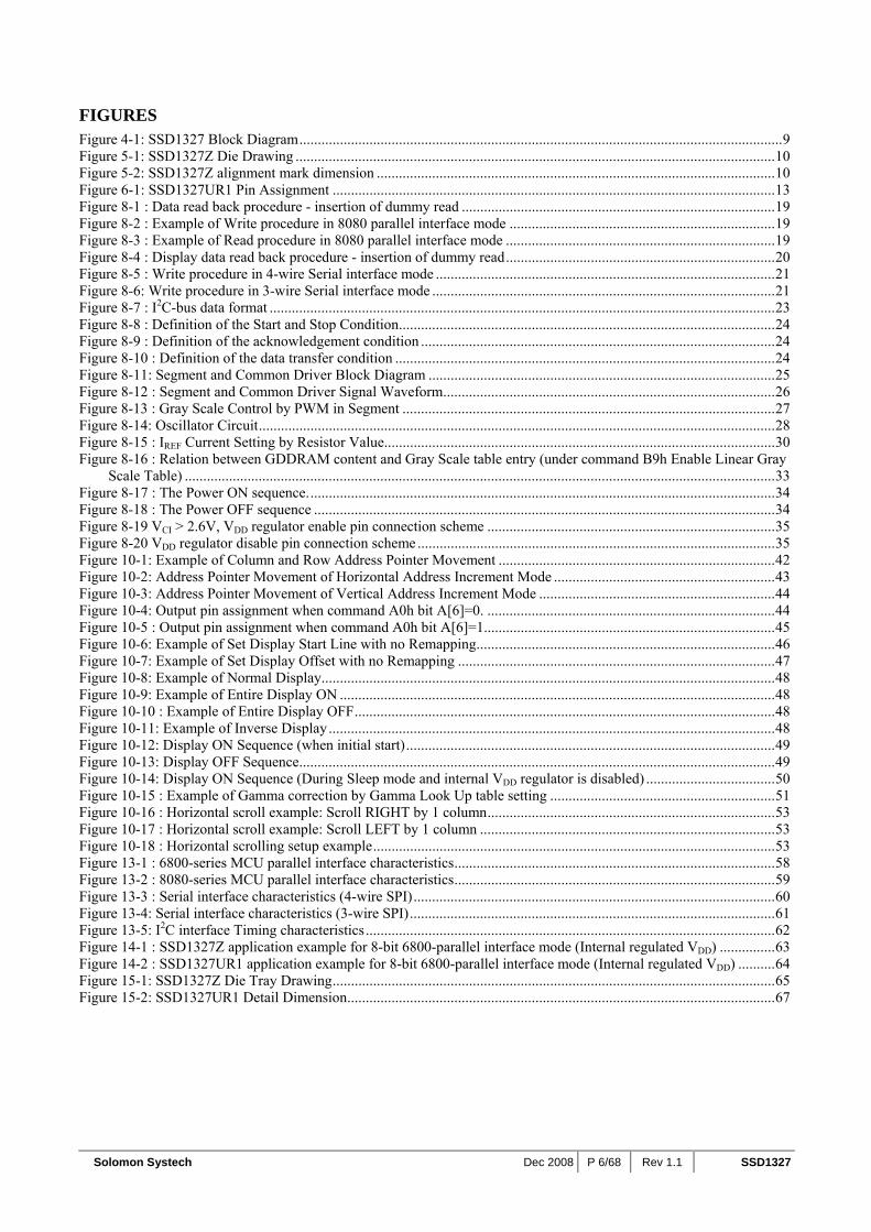
FIGURES Figure 4-1: SSD1327 Block Diagram...................................................................................................................................9 Figure 5-1: SSD1327Z Die Drawing ..................................................................................................................................10 Figure 5-2: SSD1327Z alignment mark dimension ............................................................................................................10 Figure 6-1: SSD1327UR1 Pin Assignment ........................................................................................................................13 Figure 8-1 : Data read back procedure - insertion of dummy read .....................................................................................19 Figure 8-2 : Example of Write procedure in 8080 parallel interface mode ........................................................................19 Figure 8-3 : Example of Read procedure in 8080 parallel interface mode .........................................................................19 Figure 8-4 : Display data read back procedure - insertion of dummy read.........................................................................20 Figure 8-5 : Write procedure in 4-wire Serial interface mode ............................................................................................21 Figure 8-6: Write procedure in 3-wire Serial interface mode .............................................................................................21 Figure 8-7 : I2C-bus data format .........................................................................................................................................23 Figure 8-8 : Definition of the Start and Stop Condition......................................................................................................24 Figure 8-9 : Definition of the acknowledgement condition ................................................................................................24 Figure 8-10 : Definition of the data transfer condition .......................................................................................................24 Figure 8-11: Segment and Common Driver Block Diagram ..............................................................................................25 Figure 8-12 : Segment and Common Driver Signal Waveform..........................................................................................26 Figure 8-13 : Gray Scale Control by PWM in Segment .....................................................................................................27 Figure 8-14: Oscillator Circuit............................................................................................................................................28 Figure 8-15 : IREF Current Setting by Resistor Value..........................................................................................................30 Figure 8-16 : Relation between GDDRAM content and Gray Scale table entry (under command B9h Enable Linear Gray
Scale Table) ................................................................................................................................................................33 Figure 8-17 : The Power ON sequence...............................................................................................................................34 Figure 8-18 : The Power OFF sequence .............................................................................................................................34 Figure 8-19 VCI > 2.6V, VDD regulator enable pin connection scheme ..............................................................................35 Figure 8-20 VDD regulator disable pin connection scheme .................................................................................................35 Figure 10-1: Example of Column and Row Address Pointer Movement ...........................................................................42 Figure 10-2: Address Pointer Movement of Horizontal Address Increment Mode ............................................................43 Figure 10-3: Address Pointer Movement of Vertical Address Increment Mode ................................................................44 Figure 10-4: Output pin assignment when command A0h bit A[6]=0. ..............................................................................44 Figure 10-5 : Output pin assignment when command A0h bit A[6]=1...............................................................................45 Figure 10-6: Example of Set Display Start Line with no Remapping.................................................................................46 Figure 10-7: Example of Set Display Offset with no Remapping ......................................................................................47 Figure 10-8: Example of Normal Display...........................................................................................................................48 Figure 10-9: Example of Entire Display ON ......................................................................................................................48 Figure 10-10 : Example of Entire Display OFF..................................................................................................................48 Figure 10-11: Example of Inverse Display .........................................................................................................................48 Figure 10-12: Display ON Sequence (when initial start)....................................................................................................49 Figure 10-13: Display OFF Sequence.................................................................................................................................49 Figure 10-14: Display ON Sequence (During Sleep mode and internal VDD regulator is disabled) ...................................50 Figure 10-15 : Example of Gamma correction by Gamma Look Up table setting .............................................................51 Figure 10-16 : Horizontal scroll example: Scroll RIGHT by 1 column..............................................................................53 Figure 10-17 : Horizontal scroll example: Scroll LEFT by 1 column ................................................................................53 Figure 10-18 : Horizontal scrolling setup example.............................................................................................................53 Figure 13-1 : 6800-series MCU parallel interface characteristics.......................................................................................58 Figure 13-2 : 8080-series MCU parallel interface characteristics.......................................................................................59 Figure 13-3 : Serial interface characteristics (4-wire SPI)..................................................................................................60 Figure 13-4: Serial interface characteristics (3-wire SPI)...................................................................................................61 Figure 13-5: I2C interface Timing characteristics...............................................................................................................62 Figure 14-1 : SSD1327Z application example for 8-bit 6800-parallel interface mode (Internal regulated VDD) ...............63 Figure 14-2 : SSD1327UR1 application example for 8-bit 6800-parallel interface mode (Internal regulated VDD) ..........64 Figure 15-1: SSD1327Z Die Tray Drawing........................................................................................................................65 Figure 15-2: SSD1327UR1 Detail Dimension....................................................................................................................67

SSD1327 Rev 1.1 P 7/68 Dec 2008 Solomon Systech
1 GENERAL DESCRIPTION SSD1327 is a single-chip CMOS OLED/PLED driver with controller for organic/polymer light emitting diode dot-matrix graphic display system. It consists of 128 segments and 128 commons. This IC is designed for Common Cathode type OLED/PLED panel. SSD1327 displays data directly from its internal 128 x 128 x 4 bits Graphic Display Data RAM (GDDRAM). Data/Commands are sent from general MCU through the hardware selectable I2C Interface, 6800-/8080-series compatible Parallel Interface or Serial Peripheral Interface.
2 FEATURES • Resolution: 128 x 128 matrix panel • Power supply
o VCC = 8V ~ 18V (Panel driving power supply) o VCI = 1.65V – 3.5V (MCU interface logic level & low voltage power supply) o VDD = 1.65V – 2.6V (Core VDD power supply, details refer to Table 2-1)
Table 2-1 VCI and VDD range
VCI VDD Remark 1.65 V ~ 2.6V 1.65V ~ 2.6V VDD should be tied to VCI and supplied by
external power source 2.6V ~ 3.5V 2.4V ~ 2.6V VDD is regulated from VCI o VCI must be higher than or equivalent to VDD at any circumstance
• For matrix display o Segment maximum source current: 300uA o Common maximum sink current: 40mA o 256 step contrast brightness current control
• Embedded 128 x 128 x 4 bit SRAM display buffer • 16 gray scale • Pin selectable MCU Interfaces:
o 8-bit 6800/8080-series parallel interface o 3 /4 wire Serial Peripheral Interface o I2C Interface
• Screen saving continuous scrolling function in both horizontal and vertical direction • Programmable Frame Rate • Programmable Multiplexing Ratio • Row Re-mapping and Column Re-mapping • On-Chip Oscillator • Power On Reset (POR) • Chip layout for COG , COF • Wide range of operating temperature: -40°C to 85°C

Solomon Systech Dec 2008 P 8/68 Rev 1.1 SSD1327
3 ORDERING INFORMATION
Table 3-1: Ordering Information
Ordering Part Number SEG COM Package Form Reference Remark
SSD1327Z 128 128 COG Page 10
o Min SEG pad pitch : 28um o Min COM pad pitch : 28um o Min I/O pad pitch : 60um o Die thickness: 300 +/- 15um
SSD1327UR1 128 80 COF Page 13
o Output lead pitch: 0.12mm x 0.998 = 0.11976mmo 4 SPH, 35m film o 8-bit 80 / 68 / I2C / 4 line SPI
interfaces

SSD1327 Rev 1.1 P 9/68 Dec 2008 Solomon Systech
4 BLOCK DIAGRAM
Figure 4-1: SSD1327 Block Diagram
Com
mon
Driv
ers
Se
gmen
t Driv
ers
C
omm
on D
river
s
G
ray
Scal
e D
ecod
er
Dis
play
Ti
min
g G
ener
ator
O
scill
ator
G
DD
RA
M
MC
U
Inte
rfac
e
BGGND VDD
RES#
CS# D/C#
E(RD#) R/W# (WR#)
BS0 BS1 BS2
D7 D6 D5 D4 D3 D2 D1 D0
Com
man
d D
ecod
er
.
.
.
.
.
.
.
.
.
.
.
.
.
.
.
.
.
.
.
.
.
.
COM63COM62
| |
COM1 COM0
SEG0 SEG1
| |
SEG126SEG127
CL
CLS
COM64COM65
| |
COM126COM127
.
.
.
.
.
.
.
.
.
.
.
SEG
/CO
M D
rivin
g B
lock
VCC VSS
VLSS
GPIO VSL
FR
VC
OM
H
I REF
VDD Regulator
VCI
Solomon Systech Dec 2008 P 10/68 Rev 1.1 SSD1327
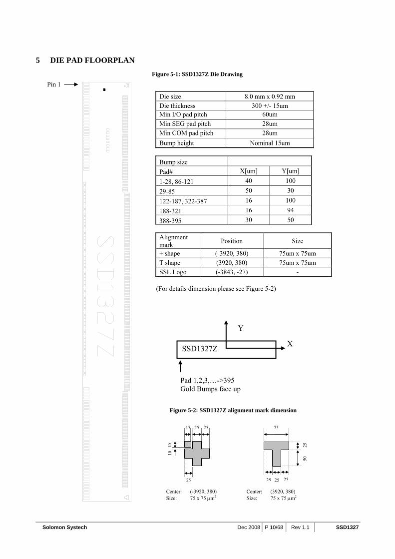
5 DIE PAD FLOORPLAN
Figure 5-1: SSD1327Z Die Drawing
Figure 5-2: SSD1327Z alignment mark dimension
Pad 1,2,3,…->395 Gold Bumps face up
SSD1327Z X
Y
Die size 8.0 mm x 0.92 mm Die thickness 300 +/- 15um Min I/O pad pitch 60um Min SEG pad pitch 28um Min COM pad pitch 28um Bump height Nominal 15um
Bump size
Pad# X[um] Y[um] 1-28, 86-121 40 100 29-85 50 30 122-187, 322-387 16 100 188-321 16 94 388-395 30 50
Alignment mark Position Size
+ shape (-3920, 380) 75um x 75um T shape (3920, 380) 75um x 75um SSL Logo (-3843, -27) -
(For details dimension please see Figure 5-2)
Pin 1
15
10
15 25 25
25
Center: (-3920, 380) Size: 75 x 75 μm2
Center: (3920, 380) Size: 75 x 75 μm2
25
50
75
2525 25

SSD1327 Rev 1.1 P 11/68 Dec 2008 Solomon Systech
Table 5-1: SSD1327Z Bump Die Pad Coordinates
Pad no. Pin name X-pos Y-pos Pad no. Pin name X-pos Y-pos Pad no. Pin name X-pos Y-pos1 NC -3947 -385 81 VLSS 1320 -420 161 COM26 2632 3502 VSL -3887 -385 82 VLSS 1385 -420 162 COM25 2604 3503 VSL -3827 -385 83 VLSS 1450 -420 163 COM24 2576 3504 VLSS -3767 -385 84 VLSS 1515 -420 164 COM23 2548 3505 VLSS -3707 -385 85 VLSS 1580 -420 165 COM22 2520 3506 VSS -3647 -385 86 VLSS 1847 -385 166 COM21 2492 3507 VSS -3587 -385 87 IREF 1907 -385 167 COM20 2464 3508 BGGND -3527 -385 88 FR 1967 -385 168 COM19 2436 3509 NC -3467 -385 89 CL 2027 -385 169 COM18 2408 350
10 VCC -3407 -385 90 VSS 2087 -385 170 COM17 2380 35011 VCC -3347 -385 91 CS# 2147 -385 171 COM16 2352 35012 VCC -3287 -385 92 RES# 2207 -385 172 COM15 2324 35013 VCOMH -3227 -385 93 D/C# 2267 -385 173 COM14 2296 35014 VCOMH -3167 -385 94 VSS 2327 -385 174 COM13 2268 35015 GPIO -3107 -385 95 R/W(WR#) 2387 -385 175 COM12 2240 35016 VDD -3047 -385 96 E(RD#) 2447 -385 176 COM11 2212 35017 VCI -2987 -385 97 D0 2507 -385 177 COM10 2184 35018 VCI -2927 -385 98 D1 2567 -385 178 COM9 2156 35019 VDD -2867 -385 99 D2 2627 -385 179 COM8 2128 35020 VDD -2807 -385 100 D3 2687 -385 180 COM7 2100 35021 VCI -2747 -385 101 D4 2747 -385 181 COM6 2072 35022 BS0 -2687 -385 102 D5 2807 -385 182 COM5 2044 35023 VSS -2627 -385 103 D6 2867 -385 183 COM4 2016 35024 BS1 -2567 -385 104 D7 2927 -385 184 COM3 1988 35025 VCI -2507 -385 105 VSS 2987 -385 185 COM2 1960 35026 BS2 -2447 -385 106 NC 3047 -385 186 COM1 1932 35027 VSS -2387 -385 107 CLS 3107 -385 187 COM0 1904 35028 VLSS -2327 -385 108 VCI 3167 -385 188 VCC 1869 39029 VLSS -2060 -420 109 VCI 3227 -385 189 VCC 1841 39030 VLSS -1995 -420 110 VDD 3287 -385 190 VCC 1813 39031 VLSS -1930 -420 111 VDD 3347 -385 191 SEG0 1778 39032 VLSS -1865 -420 112 VCOMH 3407 -385 192 SEG1 1750 39033 VLSS -1800 -420 113 VCOMH 3467 -385 193 SEG2 1722 39034 VLSS -1735 -420 114 VCC 3527 -385 194 SEG3 1694 39035 VLSS -1670 -420 115 VCC 3587 -385 195 SEG4 1666 39036 VLSS -1605 -420 116 VCC 3647 -385 196 SEG5 1638 39037 VLSS -1540 -420 117 NC 3707 -385 197 SEG6 1610 39038 VLSS -1475 -420 118 VSS 3767 -385 198 SEG7 1582 39039 VLSS -1410 -420 119 VSS 3827 -385 199 SEG8 1554 39040 VLSS -1345 -420 120 VSS 3887 -385 200 SEG9 1526 39041 VLSS -1280 -420 121 NC 3947 -385 201 SEG10 1498 39042 VLSS -1215 -420 122 NC 3724 350 202 SEG11 1470 39043 VLSS -1150 -420 123 NC 3696 350 203 SEG12 1442 39044 VLSS -1085 -420 124 COM63 3668 350 204 SEG13 1414 39045 VLSS -1020 -420 125 COM62 3640 350 205 SEG14 1386 39046 VLSS -955 -420 126 COM61 3612 350 206 SEG15 1358 39047 VLSS -890 -420 127 COM60 3584 350 207 SEG16 1330 39048 VLSS -825 -420 128 COM59 3556 350 208 SEG17 1302 39049 VLSS -760 -420 129 COM58 3528 350 209 SEG18 1274 39050 VLSS -695 -420 130 COM57 3500 350 210 SEG19 1246 39051 VLSS -630 -420 131 COM56 3472 350 211 SEG20 1218 39052 VLSS -565 -420 132 COM55 3444 350 212 SEG21 1190 39053 VLSS -500 -420 133 COM54 3416 350 213 SEG22 1162 39054 VLSS -435 -420 134 COM53 3388 350 214 SEG23 1134 39055 VLSS -370 -420 135 COM52 3360 350 215 SEG24 1106 39056 VLSS -305 -420 136 COM51 3332 350 216 SEG25 1078 39057 VLSS -240 -420 137 COM50 3304 350 217 SEG26 1050 39058 VLSS -175 -420 138 COM49 3276 350 218 SEG27 1022 39059 VLSS -110 -420 139 COM48 3248 350 219 SEG28 994 39060 VLSS -45 -420 140 COM47 3220 350 220 SEG29 966 39061 VLSS 20 -420 141 COM46 3192 350 221 SEG30 938 39062 VLSS 85 -420 142 COM45 3164 350 222 SEG31 910 39063 VLSS 150 -420 143 COM44 3136 350 223 SEG32 882 39064 VLSS 215 -420 144 COM43 3108 350 224 SEG33 854 39065 VLSS 280 -420 145 COM42 3080 350 225 SEG34 826 39066 VLSS 345 -420 146 COM41 3052 350 226 SEG35 798 39067 VLSS 410 -420 147 COM40 3024 350 227 SEG36 770 39068 VLSS 475 -420 148 COM39 2996 350 228 SEG37 742 39069 VLSS 540 -420 149 COM38 2968 350 229 SEG38 714 39070 VLSS 605 -420 150 COM37 2940 350 230 SEG39 686 39071 VLSS 670 -420 151 COM36 2912 350 231 SEG40 658 39072 VLSS 735 -420 152 COM35 2884 350 232 SEG41 630 39073 VLSS 800 -420 153 COM34 2856 350 233 SEG42 602 39074 VLSS 865 -420 154 COM33 2828 350 234 SEG43 574 39075 VLSS 930 -420 155 COM32 2800 350 235 SEG44 546 39076 VLSS 995 -420 156 COM31 2772 350 236 SEG45 518 39077 VLSS 1060 -420 157 COM30 2744 350 237 SEG46 490 39078 VLSS 1125 -420 158 COM29 2716 350 238 SEG47 462 39079 VLSS 1190 -420 159 COM28 2688 350 239 SEG48 434 39080 VLSS 1255 -420 160 COM27 2660 350 240 SEG49 406 390

Solomon Systech Dec 2008 P 12/68 Rev 1.1 SSD1327
Pad no. Pin name X-pos Y-pos Pad no. Pin name X-pos Y-pos241 SEG50 378 390 321 VCC -1869 390242 SEG51 350 390 322 COM64 -1904 350243 SEG52 322 390 323 COM65 -1932 350244 SEG53 294 390 324 COM66 -1960 350245 SEG54 266 390 325 COM67 -1988 350246 SEG55 238 390 326 COM68 -2016 350247 SEG56 210 390 327 COM69 -2044 350248 SEG57 182 390 328 COM70 -2072 350249 SEG58 154 390 329 COM71 -2100 350250 SEG59 126 390 330 COM72 -2128 350251 SEG60 98 390 331 COM73 -2156 350252 SEG61 70 390 332 COM74 -2184 350253 SEG62 42 390 333 COM75 -2212 350254 SEG63 14 390 334 COM76 -2240 350255 SEG64 -14 390 335 COM77 -2268 350256 SEG65 -42 390 336 COM78 -2296 350257 SEG66 -70 390 337 COM79 -2324 350258 SEG67 -98 390 338 COM80 -2352 350259 SEG68 -126 390 339 COM81 -2380 350260 SEG69 -154 390 340 COM82 -2408 350261 SEG70 -182 390 341 COM83 -2436 350262 SEG71 -210 390 342 COM84 -2464 350263 SEG72 -238 390 343 COM85 -2492 350264 SEG73 -266 390 344 COM86 -2520 350265 SEG74 -294 390 345 COM87 -2548 350266 SEG75 -322 390 346 COM88 -2576 350267 SEG76 -350 390 347 COM89 -2604 350268 SEG77 -378 390 348 COM90 -2632 350269 SEG78 -406 390 349 COM91 -2660 350270 SEG79 -434 390 350 COM92 -2688 350271 SEG80 -462 390 351 COM93 -2716 350272 SEG81 -490 390 352 COM94 -2744 350273 SEG82 -518 390 353 COM95 -2772 350274 SEG83 -546 390 354 COM96 -2800 350275 SEG84 -574 390 355 COM97 -2828 350276 SEG85 -602 390 356 COM98 -2856 350277 SEG86 -630 390 357 COM99 -2884 350278 SEG87 -658 390 358 COM100 -2912 350279 SEG88 -686 390 359 COM101 -2940 350280 SEG89 -714 390 360 COM102 -2968 350281 SEG90 -742 390 361 COM103 -2996 350282 SEG91 -770 390 362 COM104 -3024 350283 SEG92 -798 390 363 COM105 -3052 350284 SEG93 -826 390 364 COM106 -3080 350285 SEG94 -854 390 365 COM107 -3108 350286 SEG95 -882 390 366 COM108 -3136 350287 SEG96 -910 390 367 COM109 -3164 350288 SEG97 -938 390 368 COM110 -3192 350289 SEG98 -966 390 369 COM111 -3220 350290 SEG99 -994 390 370 COM112 -3248 350291 SEG100 -1022 390 371 COM113 -3276 350292 SEG101 -1050 390 372 COM114 -3304 350293 SEG102 -1078 390 373 COM115 -3332 350294 SEG103 -1106 390 374 COM116 -3360 350295 SEG104 -1134 390 375 COM117 -3388 350296 SEG105 -1162 390 376 COM118 -3416 350297 SEG106 -1190 390 377 COM119 -3444 350298 SEG107 -1218 390 378 COM120 -3472 350299 SEG108 -1246 390 379 COM121 -3500 350300 SEG109 -1274 390 380 COM122 -3528 350301 SEG110 -1302 390 381 COM123 -3556 350302 SEG111 -1330 390 382 COM124 -3584 350303 SEG112 -1358 390 383 COM125 -3612 350304 SEG113 -1386 390 384 COM126 -3640 350305 SEG114 -1414 390 385 COM127 -3668 350306 SEG115 -1442 390 386 NC -3696 350307 SEG116 -1470 390 387 NC -3724 350308 SEG117 -1498 390 388 TR6 -3089 25309 SEG118 -1526 390 389 TR5 -3029 25310 SEG119 -1554 390 390 TR4 -2969 25311 SEG120 -1582 390 391 VSS -2909 25312 SEG121 -1610 390 392 TR3 -2849 25313 SEG122 -1638 390 393 TR2 -2789 25314 SEG123 -1666 390 394 TR1 -2729 25315 SEG124 -1694 390 395 TR0 -2669 25316 SEG125 -1722 390317 SEG126 -1750 390318 SEG127 -1778 390319 VCC -1813 390320 VCC -1841 390

SSD1327 Rev 1.1 P 13/68 Dec 2008 Solomon Systech
6 PIN ARRANGEMENT
Figure 6-1: SSD1327UR1 Pin Assignment

Solomon Systech Dec 2008 P 14/68 Rev 1.1 SSD1327
Table 6-1: SSD1327UR1 Pin Assignment Table
PIN NO. PIN NAME PIN NO. PIN NAME PIN NO. PIN NAME PIN NO. PIN NAME1 NC 81 SEG123 161 SEG43 241 COM622 VCC 82 SEG122 162 SEG42 242 COM643 VCOMH 83 SEG121 163 SEG41 243 COM664 IREF 84 SEG120 164 SEG40 244 COM685 D7 85 SEG119 165 SEG39 245 COM706 D6 86 SEG118 166 SEG38 246 COM727 D5 87 SEG117 167 SEG37 247 COM748 D4 88 SEG116 168 SEG36 248 COM769 D3 89 SEG115 169 SEG35 249 COM7810 D2 90 SEG114 170 SEG3411 D1 91 SEG113 171 SEG3312 D0 92 SEG112 172 SEG3213 E/RD# 93 SEG111 173 SEG3114 R/W# 94 SEG110 174 SEG3015 D/C# 95 SEG109 175 SEG2916 RES# 96 SEG108 176 SEG2817 CS# 97 SEG107 177 SEG2718 NC 98 SEG106 178 SEG2619 BS2 99 SEG105 179 SEG2520 BS1 100 SEG104 180 SEG2421 VCI 101 SEG103 181 SEG2322 NC 102 SEG102 182 SEG2223 NC 103 SEG101 183 SEG2124 NC 104 SEG100 184 SEG2025 VDD 105 SEG99 185 SEG1926 NC 106 SEG98 186 SEG1827 NC 107 SEG97 187 SEG1728 NC 108 SEG96 188 SEG1629 NC 109 SEG95 189 SEG1530 VSS 110 SEG94 190 SEG1431 VSL 111 SEG93 191 SEG1332 COM79 112 SEG92 192 SEG1233 COM77 113 SEG91 193 SEG1134 COM75 114 SEG90 194 SEG1035 COM73 115 SEG89 195 SEG936 COM71 116 SEG88 196 SEG837 COM69 117 SEG87 197 SEG738 COM67 118 SEG86 198 SEG639 COM65 119 SEG85 199 SEG540 COM63 120 SEG84 200 SEG441 COM61 121 SEG83 201 SEG342 COM59 122 SEG82 202 SEG243 COM57 123 SEG81 203 SEG144 COM55 124 SEG80 204 SEG045 COM53 125 SEG79 205 NC46 COM51 126 SEG78 206 NC47 COM49 127 SEG77 207 NC48 COM47 128 SEG76 208 NC49 COM45 129 SEG75 209 NC50 COM43 130 SEG74 210 COM051 COM41 131 SEG73 211 COM252 COM39 132 SEG72 212 COM453 COM37 133 SEG71 213 COM654 COM35 134 SEG70 214 COM855 COM33 135 SEG69 215 COM1056 COM31 136 SEG68 216 COM1257 COM29 137 SEG67 217 COM1458 COM27 138 SEG66 218 COM1659 COM25 139 SEG65 219 COM1860 COM23 140 SEG64 220 COM2061 COM21 141 SEG63 221 COM2262 COM19 142 SEG62 222 COM2463 COM17 143 SEG61 223 COM2664 COM15 144 SEG60 224 COM2865 COM13 145 SEG59 225 COM3066 COM11 146 SEG58 226 COM3267 COM9 147 SEG57 227 COM3468 COM7 148 SEG56 228 COM3669 COM5 149 SEG55 229 COM3870 COM3 150 SEG54 230 COM4071 COM1 151 SEG53 231 COM4272 NC 152 SEG52 232 COM4473 NC 153 SEG51 233 COM4674 NC 154 SEG50 234 COM4875 NC 155 SEG49 235 COM5076 NC 156 SEG48 236 COM5277 SEG127 157 SEG47 237 COM5478 SEG126 158 SEG46 238 COM5679 SEG125 159 SEG45 239 COM5880 SEG124 160 SEG44 240 COM60
SSD1327 Rev 1.1 P 15/68 Dec 2008 Solomon Systech
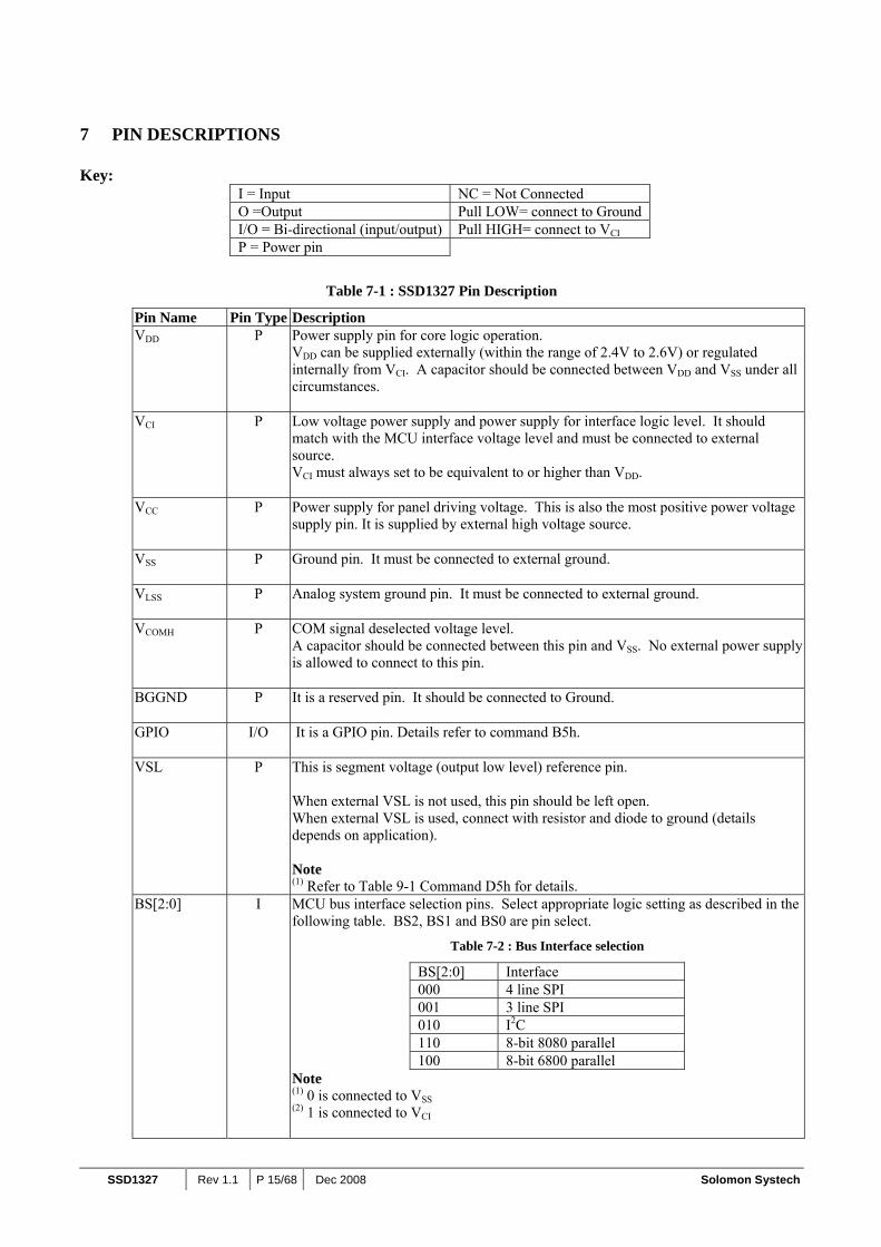
7 PIN DESCRIPTIONS Key:
I = Input NC = Not Connected O =Output Pull LOW= connect to Ground I/O = Bi-directional (input/output) Pull HIGH= connect to VCI P = Power pin
Table 7-1 : SSD1327 Pin Description
Pin Name Pin Type Description VDD P Power supply pin for core logic operation.
VDD can be supplied externally (within the range of 2.4V to 2.6V) or regulated internally from VCI. A capacitor should be connected between VDD and VSS under all circumstances.
VCI P Low voltage power supply and power supply for interface logic level. It should match with the MCU interface voltage level and must be connected to external source. VCI must always set to be equivalent to or higher than VDD.
VCC P Power supply for panel driving voltage. This is also the most positive power voltage supply pin. It is supplied by external high voltage source.
VSS P Ground pin. It must be connected to external ground.
VLSS P Analog system ground pin. It must be connected to external ground.
VCOMH P COM signal deselected voltage level. A capacitor should be connected between this pin and VSS. No external power supply is allowed to connect to this pin.
BGGND P
It is a reserved pin. It should be connected to Ground.
GPIO I/O It is a GPIO pin. Details refer to command B5h.
VSL
P This is segment voltage (output low level) reference pin. When external VSL is not used, this pin should be left open. When external VSL is used, connect with resistor and diode to ground (details depends on application). Note (1) Refer to Table 9-1 Command D5h for details.
BS[2:0] I MCU bus interface selection pins. Select appropriate logic setting as described in the following table. BS2, BS1 and BS0 are pin select.
Table 7-2 : Bus Interface selection
BS[2:0] Interface 000 4 line SPI 001 3 line SPI 010 I2C 110 8-bit 8080 parallel 100 8-bit 6800 parallel
Note (1) 0 is connected to VSS (2) 1 is connected to VCI

Solomon Systech Dec 2008 P 16/68 Rev 1.1 SSD1327
Pin Name Pin Type Description IREF I This pin is the segment output current reference pin.
A resistor should be connected between this pin and VSS to maintain the current around 10uA.
CL I External clock input pin. When internal clock is enable (i.e. pull HIGH in CLS pin), this pin is not used and should be connected to Ground. When internal clock is disable (i.e. pull LOW is CLS pin), this pin is the external clock source input pin.
CLS I Internal clock selection pin. When this pin is pulled HIGH, internal oscillator is enabled (normal operation). When this pin is pulled LOW, an external clock signal should be connected to CL.
CS# I This pin is the chip select input connecting to the MCU. The chip is enabled for MCU communication only when CS# is pulled LOW (active LOW).
RES# I This pin is reset signal input. When the pin is pulled LOW, initialization of the chip is executed. Keep this pin pull HIGH during normal operation.
D/C# I This pin is Data/Command control pin connecting to the MCU. When the pin is pulled HIGH, the data at D[7:0] will be interpreted as data. When the pin is pulled LOW, the data at D[7:0] will be transferred to a command register. In I2C mode, this pin acts as SA0 for slave address selection. When 3-wire serial interface is selected, this pin must be connected to VSS. For detail relationship to MCU interface signals, please refer to Table 8-1
R/W# (WR#) I This pin is read / write control input pin connecting to the MCU interface. When 6800 interface mode is selected, this pin will be used as Read/Write (R/W#) selection input. Read mode will be carried out when this pin is pulled HIGH and write mode when LOW. When 8080 interface mode is selected, this pin will be the Write (WR#) input. Data write operation is initiated when this pin is pulled LOW and the chip is selected. When serial or I2C interface is selected, this pin must be connected to VSS.
E (RD#) I This pin is MCU interface input. When 6800 interface mode is selected, this pin will be used as the Enable (E) signal. Read/write operation is initiated when this pin is pulled HIGH and the chip is selected. When 8080 interface mode is selected, this pin receives the Read (RD#) signal. Read operation is initiated when this pin is pulled LOW and the chip is selected. When serial or I2C interface is selected, this pin must be connected to VSS.

SSD1327 Rev 1.1 P 17/68 Dec 2008 Solomon Systech
Pin Name Pin Type Description D[7:0] I/O These pins are bi-directional data bus connecting to the MCU data bus.
Unused pins are recommended to tie LOW. When serial interface mode is selected, D0 will be the serial clock input: SCLK; D1 will be the serial data input: SDIN and D2 should be kept NC. When I2C mode is selected, D2, D1 should be tied together and serve as SDAout, SDAin in application and D0 is the serial clock input, SCL.
FR O This pin outputs RAM write synchronization signal. Proper timing between MCU data writing and frame display timing can be achieved to prevent tearing effect. It should be kept NC if it is not used.
TR[6:0] - Reserved pin and must be kept float.
SEG0 ~ SEG127
O These pins provide the OLED segment driving signals. These pins are VSS state when display is OFF.
COM0 ~ COM127
I/O These pins provide the Common switch signals to the OLED panel. These pins are in high impedance state when display is OFF.

Solomon Systech Dec 2008 P 18/68 Rev 1.1 SSD1327
8 FUNCTIONAL BLOCK DESCRIPTIONS
8.1 MCU Interface selection SSD1327 MCU interface consist of 8 data pins and 5 control pins. The pin assignment at different interface mode is summarized in Table 8-1. Different MCU mode can be set by hardware selection on BS[2:0] pins (please refer to Table 7-2 for BS[2:0] setting).
Table 8-1 : MCU interface assignment under different bus interface mode
Data/Command Interface Control Signal Pin Name Bus Interface D7 D6 D5 D4 D3 D2 D1 D0 E R/W# CS# D/C# RES# 8-bit 8080 D[7:0] RD# WR# CS# D/C# RES# 8-bit 6800 D[7:0] E R/W# CS# D/C# RES# 3-wire SPI Tie LOW NC SDIN SCLK Tie LOW CS# Tie LOW RES# 4-wire SPI Tie LOW NC SDIN SCLK Tie LOW CS# D/C# RES# I2C Tie LOW SDAOUT SDAIN SCL Tie LOW SA0 RES#
8.1.1 MCU Parallel 6800-series Interface The parallel interface consists of 8 bi-directional data pins (D[7:0]), R/W#, D/C#, E and CS#. A LOW in R/W# indicates WRITE operation and HIGH in R/W# indicates READ operation. A LOW in D/C# indicates COMMAND read/write and HIGH in D/C# indicates DATA read/write. The E input serves as data latch signal while CS# is LOW. Data is latched at the falling edge of E signal.
Table 8-2 : Control pins of 6800 interface
Function E R/W# CS# D/C#
Write command ↓ L L L
Read status ↓ H L L
Write data ↓ L L H
Read data ↓ H L H Note (1) ↓ stands for falling edge of signal H stands for HIGH in signal L stands for LOW in signal In order to match the operating frequency of display RAM with that of the microprocessor, some pipeline processing is internally performed which requires the insertion of a dummy read before the first actual display data read. This is shown in Figure 8-1.

SSD1327 Rev 1.1 P 19/68 Dec 2008 Solomon Systech
Figure 8-1 : Data read back procedure - insertion of dummy read
N n n+1 n+2
R/W#
E
Databus
Write columnaddress Read 1st dataDummy read Read 2nd data Read 3rd data
8.1.2 MCU Parallel 8080-series Interface The parallel interface consists of 8 bi-directional data pins (D[7:0]), RD#, WR#, D/C# and CS#. A LOW in D/C# indicates COMMAND read/write and HIGH in D/C# indicates DATA read/write. A rising edge of RD# input serves as a data READ latch signal while CS# is kept LOW. A rising edge of WR# input serves as a data/command WRITE latch signal while CS# is kept LOW.
Figure 8-2 : Example of Write procedure in 8080 parallel interface mode
CS#
WR#
D[7:0]
D/C#
RD#high
low
Figure 8-3 : Example of Read procedure in 8080 parallel interface mode
CS#
WR#
D[7:0]
D/C#
RD#
high
low

Solomon Systech Dec 2008 P 20/68 Rev 1.1 SSD1327
Table 8-3 : Control pins of 8080 interface
Function RD# WR# CS# D/C# Write command H ↑ L L Read status ↑ H L L Write data H ↑ L H Read data ↑ H L H
Note (1) ↑ stands for rising edge of signal (2) H stands for HIGH in signal (3) L stands for LOW in signal In order to match the operating frequency of display RAM with that of the microprocessor, some pipeline processing is internally performed which requires the insertion of a dummy read before the first actual display data read. This is shown in Figure 8-4.
Figure 8-4 : Display data read back procedure - insertion of dummy read
N n n+1 n+2
WR#
RD#
Databus
Write columnaddress Read 1st dataDummy read Read 2nd data Read 3rd data
8.1.3 MCU Serial Interface (4-wire SPI) The serial interface consists of serial clock SCLK, serial data SDIN, D/C#, CS#. In SPI mode, D0 acts as SCLK, D1 acts as SDIN. For the unused data pins, D2 should be left open. The pins from D3 to D7, E and R/W# can be connected to an external ground.
Table 8-4 : Control pins of 4-wire Serial interface
Function E(RD#) R/W#(WR#) CS# D/C# D0 Write command Tie LOW Tie LOW L L ↑ Write data Tie LOW Tie LOW L H ↑
Note (1) H stands for HIGH in signal (2) L stands for LOW in signal SDIN is shifted into an 8-bit shift register on every rising edge of SCLK in the order of D7, D6, ... D0. D/C# is sampled on every eighth clock and the data byte in the shift register is written to the Graphic Display Data RAM (GDDRAM) or command register in the same clock. Under serial mode, only write operations are allowed.

SSD1327 Rev 1.1 P 21/68 Dec 2008 Solomon Systech
Figure 8-5 : Write procedure in 4-wire Serial interface mode
8.1.4 MCU Serial Interface (3-wire SPI) The 3-wire serial interface consists of serial clock SCLK, serial data SDIN and CS#. In 3-wire SPI mode, D0 acts as SCLK, D1 acts as SDIN. For the unused data pins, D2 should be left open. The pins from D3 to D7, R/W# (WR#), E(RD#) and D/C# can be connected to an external ground. The operation is similar to 4-wire serial interface while D/C# pin is not used. There are altogether 9-bits will be shifted into the shift register on every ninth clock in sequence: D/C# bit, D7 to D0 bit. The D/C# bit (first bit of the sequential data) will determine the following data byte in the shift register is written to the Display Data RAM (D/C# bit = 1) or the command register (D/C# bit = 0). Under serial mode, only write operations are allowed.
Table 8-5: Control pins of 3-wire Serial interface
Function E(RD#) R/W#(WR#) CS# D/C# D0Write command Tie LOW Tie LOW L Tie LOW ↑Write data Tie LOW Tie LOW L Tie LOW ↑
Note (1) L stands for LOW in signal
Figure 8-6: Write procedure in 3-wire Serial interface mode
D7 D6 D5 D4 D3 D2 D1 D0
SCLK (D0)
SDIN(D1)
DB1 DB2 DBn
CS#
D/C#
SDIN/ SCLK
D7 D6 D5 D4 D3 D2 D1 D0
SCLK(D0)
SDIN(D1)
DB1 DB2 DBn
CS#
D/C#
SDIN/ SCLK

Solomon Systech Dec 2008 P 22/68 Rev 1.1 SSD1327
8.1.5 MCU I2C Interface The I2C communication interface consists of slave address bit SA0, I2C-bus data signal SDA (SDAOUT/D2 for output and SDAIN/D1 for input) and I2C-bus clock signal SCL (D0). Both the data and clock signals must be connected to pull-up resistors. RES# is used for the initialization of device.
a) Slave address bit (SA0) SSD1327 has to recognize the slave address before transmitting or receiving any information by the I2C-bus. The device will respond to the slave address following by the slave address bit (“SA0” bit) and the read/write select bit (“R/W#” bit) with the following byte format, b7 b6 b5 b4 b3 b2 b1 b0 0 1 1 1 1 0 SA0 R/W# “SA0” bit provides an extension bit for the slave address. Either “0111100” or “0111101”, can be selected as the slave address of SSD1327. D/C# pin acts as SA0 for slave address selection. “R/W#” bit is used to determine the operation mode of the I2C-bus interface. R/W#=1, it is in read mode. R/W#=0, it is in write mode.
b) I2C-bus data signal (SDA) SDA acts as a communication channel between the transmitter and the receiver. The data and the acknowledgement are sent through the SDA. It should be noticed that the ITO track resistance and the pulled-up resistance at “SDA” pin becomes a voltage potential divider. As a result, the acknowledgement would not be possible to attain a valid logic 0 level in “SDA”. “SDAIN” and “SDAOUT” are tied together and serve as SDA. The “SDAIN” pin must be connected to act as SDA. The “SDAOUT” pin may be disconnected. When “SDAOUT” pin is disconnected, the acknowledgement signal will be ignored in the I2C-bus.
c) I2C-bus clock signal (SCL) The transmission of information in the I2C-bus is following a clock signal, SCL. Each transmission of data bit is taken place during a single clock period of SCL.

SSD1327 Rev 1.1 P 23/68 Dec 2008 Solomon Systech
8.1.5.1 I2C-bus Write data The I2C-bus interface gives access to write data and command into the device. Please refer to Figure 8-7 for the write mode of I2C-bus in chronological order.
Figure 8-7 : I2C-bus data format
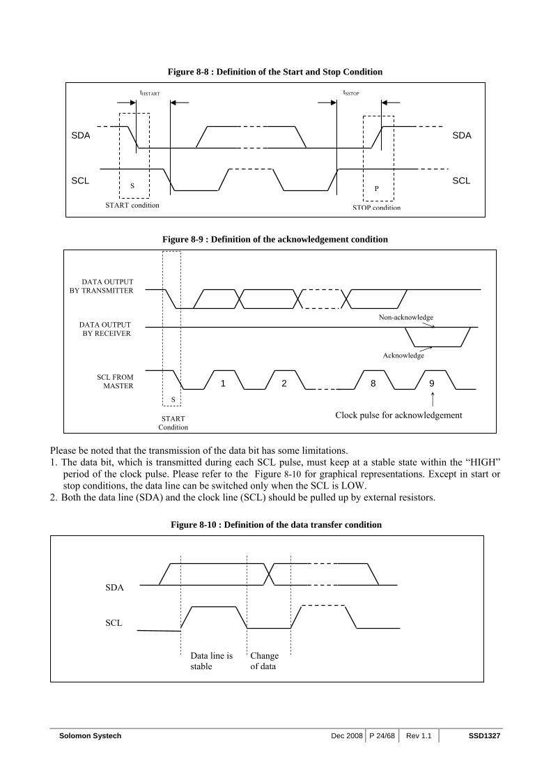
8.1.5.2 Write mode for I2C 1) The master device initiates the data communication by a start condition. The definition of the start
condition is shown in Figure 8-8. The start condition is established by pulling the SDA from HIGH to LOW while the SCL stays HIGH.
2) The slave address is following the start condition for recognition use. For the SSD1327, the slave address is either “b0111100” or “b0111101” by changing the SA0 to LOW or HIGH (D/C pin acts as SA0).
3) The write mode is established by setting the R/W# bit to logic “0”. 4) An acknowledgement signal will be generated after receiving one byte of data, including the slave
address and the R/W# bit. Please refer to the Figure 8-9 for the graphical representation of the acknowledge signal. The acknowledge bit is defined as the SDA line is pulled down during the HIGH period of the acknowledgement related clock pulse.
5) After the transmission of the slave address, either the control byte or the data byte may be sent across the SDA. A control byte mainly consists of Co and D/C# bits following by six “0” ‘s.
a. If the Co bit is set as logic “0”, the transmission of the following information will contain data bytes only.
b. The D/C# bit determines the next data byte is acted as a command or a data. If the D/C# bit is set to logic “0”, it defines the following data byte as a command. If the D/C# bit is set to logic “1”, it defines the following data byte as a data which will be stored at the GDDRAM. The GDDRAM column address pointer will be increased by one automatically after each data write.
6) Acknowledge bit will be generated after receiving each control byte or data byte. 7) The write mode will be finished when a stop condition is applied. The stop condition is also defined
in Figure 8-8. The stop condition is established by pulling the “SDA in” from LOW to HIGH while the “SCL” stays HIGH.
0 1 1 1 1
P
Slave Address m ≥ 0 words n ≥ 0 bytes MSB ……………….LSB
1 byte
Write mode
SSD1327 Slave Address
R/W
#
D/C
#C
o A
CK
AC
KControl byte Data byte Control byte
AC
K Data byte
AC
K
S
0 1 1 1 1 0
SA
0 R
/W#
Co
D/C
AC
K
Control byte
Note: Co – Continuation bit D/C# – Data / Command Selection bit ACK – Acknowledgement SA0 – Slave address bit R/W# – Read / Write Selection bit S – Start Condition / P – Stop Condition
0 0 0 0 0 0
0 1 1 1 1 0
D/C
#C
o A
CK
SA
0
Solomon Systech Dec 2008 P 24/68 Rev 1.1 SSD1327
Figure 8-8 : Definition of the Start and Stop Condition
Figure 8-9 : Definition of the acknowledgement condition
Please be noted that the transmission of the data bit has some limitations. 1. The data bit, which is transmitted during each SCL pulse, must keep at a stable state within the “HIGH”
period of the clock pulse. Please refer to the Figure 8-10 for graphical representations. Except in start or stop conditions, the data line can be switched only when the SCL is LOW.
2. Both the data line (SDA) and the clock line (SCL) should be pulled up by external resistors.
Figure 8-10 : Definition of the data transfer condition
SDA
SCL
Data line is stable
Change of data
S
START condition
SDA
SCL P
STOP condition
SDA
SCL
tHSTART tSSTOP
DATA OUTPUT BY RECEIVER
DATA OUTPUT BY TRANSMITTER
SCL FROM MASTER
S
START Condition
Clock pulse for acknowledgement
1 8 9
Non-acknowledge
2
Acknowledge
SSD1327 Rev 1.1 P 25/68 Dec 2008 Solomon Systech
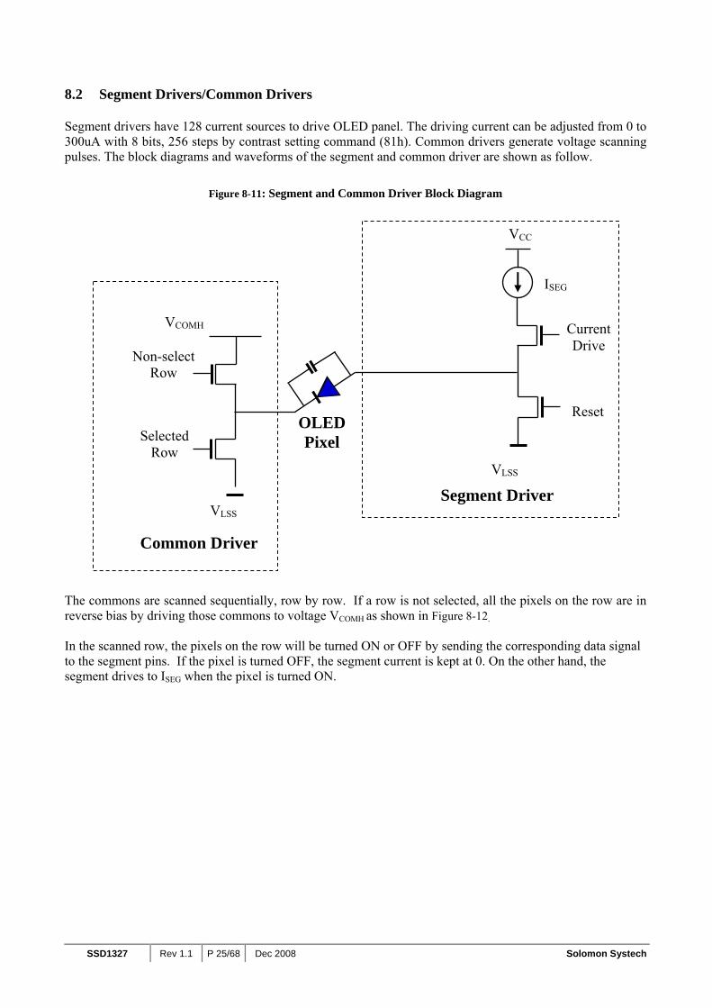
8.2 Segment Drivers/Common Drivers Segment drivers have 128 current sources to drive OLED panel. The driving current can be adjusted from 0 to 300uA with 8 bits, 256 steps by contrast setting command (81h). Common drivers generate voltage scanning pulses. The block diagrams and waveforms of the segment and common driver are shown as follow.
Figure 8-11: Segment and Common Driver Block Diagram
The commons are scanned sequentially, row by row. If a row is not selected, all the pixels on the row are in reverse bias by driving those commons to voltage VCOMH as shown in Figure 8-12. In the scanned row, the pixels on the row will be turned ON or OFF by sending the corresponding data signal to the segment pins. If the pixel is turned OFF, the segment current is kept at 0. On the other hand, the segment drives to ISEG when the pixel is turned ON.
VCOMH
Non-select Row
Selected Row
VCC
Current Drive
Reset
VLSS
VLSS
Common Driver
Segment Driver
OLED Pixel
ISEG

Solomon Systech Dec 2008 P 26/68 Rev 1.1 SSD1327
Figure 8-12 : Segment and Common Driver Signal Waveform
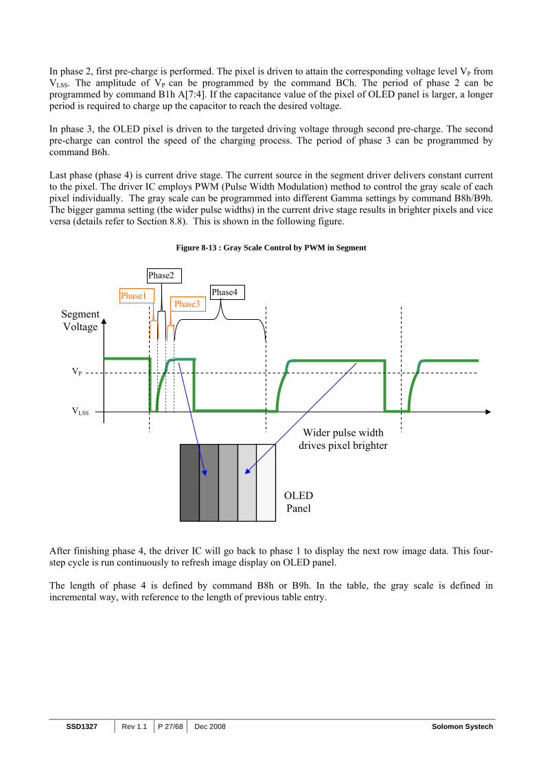
There are four phases to driving an OLED a pixel. In phase 1, the pixel is reset by the segment driver to VLSS in order to discharge the previous data charge stored in the parasitic capacitance along the segment electrode. The period of phase 1 can be programmed by command B1h A[3:0]. An OLED panel with larger capacitance requires a longer period for discharging.
C OM 1 V COMH
V LS S
V COMH
V LS S
COM 0 One Frame Period Non-selected Row
Selected Row
COM Voltage
V COMH
V LS S
This row is selected toturn on
TimeSegment Voltage
V LS S
Waveform for ON
Waveform for OFF
Time
V P
SSD1327 Rev 1.1 P 27/68 Dec 2008 Solomon Systech
In phase 2, first pre-charge is performed. The pixel is driven to attain the corresponding voltage level VP from VLSS. The amplitude of VP can be programmed by the command BCh. The period of phase 2 can be programmed by command B1h A[7:4]. If the capacitance value of the pixel of OLED panel is larger, a longer period is required to charge up the capacitor to reach the desired voltage. In phase 3, the OLED pixel is driven to the targeted driving voltage through second pre-charge. The second pre-charge can control the speed of the charging process. The period of phase 3 can be programmed by command B6h. Last phase (phase 4) is current drive stage. The current source in the segment driver delivers constant current to the pixel. The driver IC employs PWM (Pulse Width Modulation) method to control the gray scale of each pixel individually. The gray scale can be programmed into different Gamma settings by command B8h/B9h. The bigger gamma setting (the wider pulse widths) in the current drive stage results in brighter pixels and vice versa (details refer to Section 8.8). This is shown in the following figure.
Figure 8-13 : Gray Scale Control by PWM in Segment
After finishing phase 4, the driver IC will go back to phase 1 to display the next row image data. This four-step cycle is run continuously to refresh image display on OLED panel. The length of phase 4 is defined by command B8h or B9h. In the table, the gray scale is defined in incremental way, with reference to the length of previous table entry.
Segment Voltage
VLSS
OLED Panel
Wider pulse width drives pixel brighter
Phase1
Phase2
Phase3 Phase4
VP

Solomon Systech Dec 2008 P 28/68 Rev 1.1 SSD1327
8.3 Oscillator Circuit and Display Time Generator This module is an On-Chip low power RC oscillator circuitry (Figure 8-14). The operation clock (CLK) can be generated either from internal oscillator or external source CL pin. This selection is done by CLS pin. If CLS pin is HIGH, internal oscillator is chosen and CL should be pulled to LOW. If CLS pin is LOW, external clock from CL pin will be used for CLK for proper operation. The frequency of internal oscillator FOSC can be programmed by command B3h.
Figure 8-14: Oscillator Circuit
Divider
InternalOscillator
FoscMUXCL
CLK DCLK
DisplayClock
CLS
The display clock (DCLK) for the Display Timing Generator is derived from CLK. The division factor “D” can be programmed from 1 to 16 by command B3h.
DCLK = FOSC / D The frame frequency of display is determined by the following formula:
MuxofNo.K DF
F oscFRM ××
=
where • D stands for clock divide ratio. It is set by command B3h A[3:0]. The divide ratio has the range from 1 to
16. • K is the number of display clocks per row. The value is derived by
K = Phase 1 period + Phase 2 period + X X = DCLKs in current drive period; Default X = 30 Default K is 4 + 7 + 30 = 41
• Number of multiplex ratio is set by command A8h. The reset value is 127 (i.e. 128MUX). • Fosc is the oscillator frequency. It can be changed by command B3h A[7:4]. The higher the register setting
results in higher frequency. If the frame frequency is set too low, flickering may occur. On the other hand, higher frame frequency leads to higher power consumption on the whole system.

SSD1327 Rev 1.1 P 29/68 Dec 2008 Solomon Systech
8.4 Command Decoder and Command Interface This module determines whether the input data is interpreted as data or command. Data is interpreted based upon the input of the D/C# pin. If D/C# pin is HIGH, the input at D7-D0 is written to Graphic Display Data RAM (GDDRAM). If it is LOW, the input at D7-D0 is interpreted as a Command which will be decoded and be written to the corresponding command register.
8.5 Reset Circuit When RES# input is LOW, the chip is initialized with the following status:
1. Display is OFF 2. 128 x 128 Display Mode 3. Normal segment and display data column address and row address mapping (SEG0 mapped to
address 00h and COM0 mapped to address 00h) 4. Shift register data clear in serial interface 5. Display start line is set at display RAM address 0 6. Column address counter is set at 0 7. Normal scan direction of the COM outputs 8. Contrast control register is set at 7Fh 9. Normal display mode (Equivalent to A4h command)
8.6 SEG/COM Driving Block This block is used to derive the incoming power sources into the different levels of internal use voltage and current.
• VCC is the most positive voltage supply. • VCOMH is the Common deselected level. It is internally regulated. • VLSS is the ground path of the analog and panel current. • IREF is a reference current source for segment current drivers ISEG. The relationship between reference
current and segment current of a color is:
ISEG = Contrast / 256 * IREF * scale factor in which
the contrast (0~255) is set by Set Contrast command (81h).
For example, in order to achieve ISEG = 300uA at maximum contrast 255, IREF is set to around 10uA. This current value is obtained by connecting an appropriate resistor from IREF pin to VSS as shown in Figure 8-15.

Solomon Systech Dec 2008 P 30/68 Rev 1.1 SSD1327
Figure 8-15 : IREF Current Setting by Resistor Value
Recommended IREF = 10uA. Since the voltage at IREF pin is VCC – 3V, the value of resistor R1 can be found as below:
For IREF = 10uA, VCC = 12V: R1 = (Voltage at IREF – VSS) / IREF
= (12 – 3) / 10uA ≈ 910kΩ
8.7 Graphic Display Data RAM (GDDRAM) The GDDRAM is a bit mapped static RAM holding the bit pattern to be displayed. The size of the RAM is 128x128x4 bits. For mechanical flexibility, re-mapping on both Segment and Common outputs can be selected by software. The GDDRAM address maps in Table 8-6 to Table 8-10 show some examples on using the command “Set Re-map” A0h to re-map the GDDRAM. In the following tables, the lower nibble and higher nibble of D0, D1, D2 … D8189, D8190, D8191 represent the 128x128 data bytes in the GDDRAM. Table 8-6 shows the GDDRAM map under the following condition: • Command “Set Re-map” A0h is set to:
Disable Column Address Re-map (A[0]=0)Disable Nibble Re-map (A[1]=0)Enable Horizontal Address Increment (A[2]=0)Disable COM Re-map (A[4]=0)
• Display Start Line=00h • Data byte sequence: D0, D1, D2 … D8191
Table 8-6 : GDDRAM address map 1
SSD1327
IREF (voltage at this pin = VCC – 3)
R1
VSS
IREF ≈ 10uA
Nibble re-map A[1]=0
SEG Outputs
Column Address
COM0 00 (HEX)
COM1 01
| | |
COM126 7E
COM127 7F
COMOutputs
RowAddress(HEX)
3E 3F00 01
D0[3:0] D0[7:4]
D64[3:0] D64[7:4]
D1[3:0] D1[7:4]
D65[3:0] D65[7:4]
D8064[3:0] D8064[7:4] D8065[3:0] D8065[7:4]
D8128[3:0] D8128[7:4] D8129[3:0] D8129[7:4]
D62[3:0] D62[7:4] D63[3:0] D63[7:4]
D126[3:0] D126[7:4] D127[3:0] D127[7:4]
D8126[3:0] D8126[7:4] D8127[3:0] D8127[7:4]
D8190[3:0] D8190[7:4] D8191[3:0] D8191[7:4]
SEG0 SEG1 SEG2 SEG127SEG3 SEG124 SEG125 SEG126

SSD1327 Rev 1.1 P 31/68 Dec 2008 Solomon Systech
Table 8-7 shows the GDDRAM map under the following condition: • Command “Set Re-map” A0h is set to:
Disable Column Address Re-map (A[0]=0)Disable Nibble Re-map (A[1]=0)Enable Vertical Address Increment (A[2]=1)Disable COM Re-map (A[4]=0)
• Display Start Line=00h • Data byte sequence: D0, D1, D2 … D8191
Table 8-7 : GDDRAM address map 2
Table 8-8 shows the GDDRAM map under the following condition: • Command “Set Re-map” A0h is set to:
Enable Column Address Re-map (A[0]=1)Enable Nibble Re-map (A[1]=1)Enable Horizontal Address Increment (A[2]=0)Disable COM Re-map (A[4]=0)
• Display Start Line=00h • Data byte sequence: D0, D1, D2 … D8191
Table 8-8 : GDDRAM address map 3
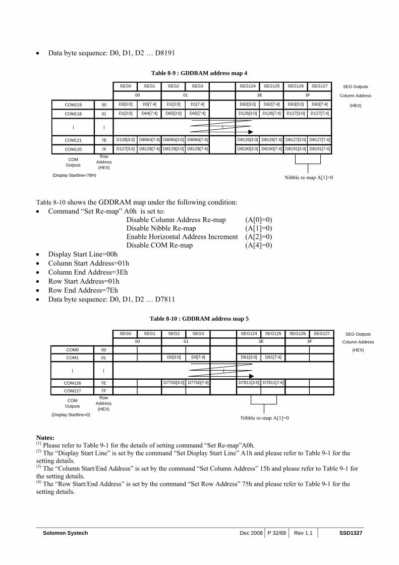
Table 8-9 shows the example in which the display start line register is set to 10h with the following condition: • Command “Set Re-map” A0h is set to:
Disable Column Address Re-map (A[0]=0)Disable Nibble Re-map (A[1]=0)Enable Horizontal Address Increment (A[2]=0)Enable COM Re-map (A[4]=1)
• Display Start Line=78h (corresponds to COM119)
Nibble re-map A[1]=0
SEG Outputs
Column Address
COM0 00 (HEX)
COM1 01
| | |
COM126 7E
COM127 7F
COMOutputs
RowAddress(HEX)
(Display Startline=0)
D0[3:0] D0[7:4] D128[3:0] D128[7:4]
D1[3:0] D1[7:4] D129[3:0] D129[7:4]
D126[3:0] D126[7:4] D254[3:0] D254[7:4]
D127[3:0] D127[7:4] D255[3:0] D255[7:4]
D7936[3:0] D7936[7:4] D8064[3:0] D8064[7:4]
D7937[3:0] D7937[7:4] D8065[3:0] D8065[7:4]
D8062[3:0] D8062[7:4] D8190[3:0] D8190[7:4]
D8063[3:0] D8063[7:4] D8191[3:0] D8191[7:4]
00 01 3E 3F
SEG124 SEG125 SEG126 SEG127SEG0 SEG1 SEG2 SEG3
Nibble re-map A[1]=1
SEG Outputs
Column Address
COM0 00 (HEX)
COM1 01
| | |
COM126 7E
COM127 7F
COMOutputs
RowAddress(HEX)
(Display Startline=0)
3F 3E 01 00
SEG124 SEG125 SEG126 SEG127SEG0 SEG1 SEG2 SEG3
D8129[7:4] D8129[3:0] D8128[7:4] D8128[3:0]D8191[7:4] D8191[3:0] D8190[7:4] D8190[3:0]
D8065[7:4] D8065[3:0] D8064[7:4] D8064[3:0]D8127[7:4] D8127[3:0] D8126[7:4] D8126[3:0]
D65[7:4] D65[3:0] D64[7:4] D64[3:0]D127[7:4] D127[3:0] D126[7:4] D126[3:0]
D1[7:4] D1[3:0] D0[7:4] D0[3:0]D63[7:4] D63[3:0] D62[7:4] D62[3:0]
Solomon Systech Dec 2008 P 32/68 Rev 1.1 SSD1327
• Data byte sequence: D0, D1, D2 … D8191
Table 8-9 : GDDRAM address map 4
Table 8-10 shows the GDDRAM map under the following condition: • Command “Set Re-map” A0h is set to:
Disable Column Address Re-map (A[0]=0)Disable Nibble Re-map (A[1]=0)Enable Horizontal Address Increment (A[2]=0)Disable COM Re-map (A[4]=0)
• Display Start Line=00h • Column Start Address=01h • Column End Address=3Eh • Row Start Address=01h • Row End Address=7Eh • Data byte sequence: D0, D1, D2 … D7811
Table 8-10 : GDDRAM address map 5
Notes: (1] Please refer to Table 9-1 for the details of setting command “Set Re-map”A0h. (2) The “Display Start Line” is set by the command “Set Display Start Line” A1h and please refer to Table 9-1 for the setting details. (3) The “Column Start/End Address” is set by the command “Set Column Address” 15h and please refer to Table 9-1 for the setting details. (4) The “Row Start/End Address” is set by the command “Set Row Address” 75h and please refer to Table 9-1 for the setting details.
Nibble re-map A[1]=0
SEG Outputs
Column Address
COM119 00 (HEX)
COM118 01
| | |
COM121 7E
COM120 7F
COMOutputs
RowAddress(HEX)
(Display Startline=78H)
D63[3:0] D63[7:4]
00 01
D62[3:0] D62[7:4]D0[3:0] D0[7:4] D1[3:0] D1[7:4]
D1[3:0] D64[7:4] D65[3:0] D65[7:4]
3E 3F
D126[3:0] D126[7:4] D127[3:0] D127[7:4]
D126[3:0] D8064[7:4] D8065[3:0] D8065[7:4] D8127[3:0] D8127[7:4]
D127[3:0] D8128[7:4] D8129[3:0] D8129[7:4]
D8126[3:0] D8126[7:4]
D8190[3:0] D8190[7:4] D8191[3:0] D8191[7:4]
SEG0 SEG1 SEG2 SEG3 SEG124 SEG125 SEG126 SEG127
Nibble re-map A[1]=0
SEG Outputs
Column Address
COM0 00 (HEX)
COM1 01
| | |
COM126 7E
COM127 7F
COMOutputs
RowAddress(HEX)
(Display Startline=0)
SEG124SEG0 SEG125 SEG126 SEG127
00 01 3E 3F
SEG1 SEG2 SEG3
D0[3:0] D0[7:4] D61[3:0] D61[7:4]
D7750[3:0] D7750[7:4] D7811[3:0] D7811[7:4]

SSD1327 Rev 1.1 P 33/68 Dec 2008 Solomon Systech
8.8 Gray Scale Decoder The gray scale effect is generated by controlling the pulse width (PW) of current drive phase, except GS0 there is no pre-charge (phase 2, 3) and current drive (phase 4). The driving period is controlled by the gray scale settings (setting 0 ~ setting 127). The larger the setting, the brighter the pixel will be. The Gray Scale Table stores the corresponding gray scale setting of the 16 gray scale levels (GS0~GS15) through the software commands B8h or B9h. As shown in Figure 8-16, GDDRAM data has 4 bits, represent the 16 gray scale levels from GS0 to GS15. Note that the frame frequency is affected by GS15 setting. Figure 8-16 : Relation between GDDRAM content and Gray Scale table entry (under command B9h Enable Linear Gray Scale
Table)
GDDRAM data (4 bits) Gray Scale Table Default Gamma Setting (Command B9h)
0000 GS0 Setting 0 0001 GS1 (1) Setting 0 0010 GS2 Setting 2 0011 GS3 Setting 4
: : : : : :
1101 GS13 Setting 24 1110 GS14 Setting 26 1111 GS15 Setting 28
Note: (1) Both GS0 and GS1 have no 2nd pre-charge (phase 3) and current drive (phase 4), however GS1 has 1st pre-charge (phase 2).
Solomon Systech Dec 2008 P 34/68 Rev 1.1 SSD1327
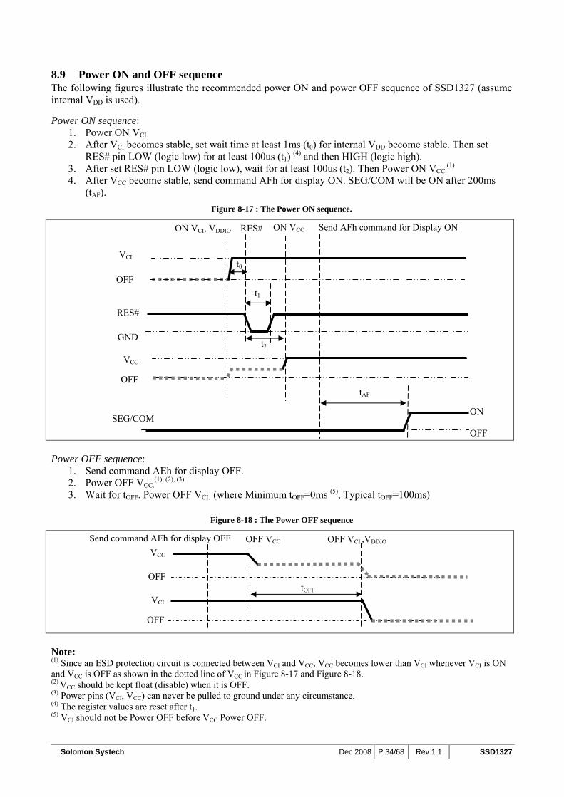
8.9 Power ON and OFF sequence The following figures illustrate the recommended power ON and power OFF sequence of SSD1327 (assume internal VDD is used). Power ON sequence:
1. Power ON VCI. 2. After VCI becomes stable, set wait time at least 1ms (t0) for internal VDD become stable. Then set
RES# pin LOW (logic low) for at least 100us (t1) (4) and then HIGH (logic high). 3. After set RES# pin LOW (logic low), wait for at least 100us (t2). Then Power ON VCC.
(1) 4. After VCC become stable, send command AFh for display ON. SEG/COM will be ON after 200ms
(tAF). Figure 8-17 : The Power ON sequence.
Power OFF sequence:
1. Send command AEh for display OFF. 2. Power OFF VCC.
(1), (2), (3) 3. Wait for tOFF. Power OFF VCI.
(where Minimum tOFF=0ms (5), Typical tOFF=100ms)
Figure 8-18 : The Power OFF sequence
Note: (1) Since an ESD protection circuit is connected between VCI and VCC, VCC becomes lower than VCI whenever VCI is ON and VCC is OFF as shown in the dotted line of VCC in Figure 8-17 and Figure 8-18. (2)
VCC should be kept float (disable) when it is OFF. (3) Power pins (VCI, VCC) can never be pulled to ground under any circumstance. (4) The register values are reset after t1. (5) VCI should not be Power OFF before VCC Power OFF.
OFF VCI ,VDDIO
VCI
VCC Send command AEh for display OFF OFF VCC
OFF
OFF tOFF
OFF
ON VCI, VDDIO RES# ON VCC Send AFh command for Display ON
VCI
RES#
OFF
t1
SEG/COM
tAF
ON OFF
VCC
GND t2
t0

SSD1327 Rev 1.1 P 35/68 Dec 2008 Solomon Systech
8.10 VDD Regulator In SSD1327, the power supply pin for core logic operation, VDD, can be supplied by external source or internally regulated through the VDD regulator. The internal VDD regulator is enabled by setting bit A[0] to 1b in command ABh “Function Selection”. VCI should be larger than 2.6V when using the internal VDD regulator. The typical regulated VDD is about 2.5V It should be notice that, no matter VDD is supplied by external source or internally regulated; VCI must always be set equivalent to or higher than VDD. The following figure shows the VDD regulator pin connection scheme:
Figure 8-19 VCI > 2.6V, VDD regulator enable pin connection scheme
Figure 8-20 VDD regulator disable pin connection scheme
No RAM access through MCU interface when there is no external / internal VDD.
CI
V CI V SS VDD
V
V CI > 2.6V, VDD Regulator Enable,Command: ABh A[0]=1b.
GND
CI GND
V CI V SS VDD
V
VDD Regulator Disable,Command: ABh A[0]=0b.
VDD
Solomon Systech Dec 2008 P 36/68 Rev 1.1 SSD1327
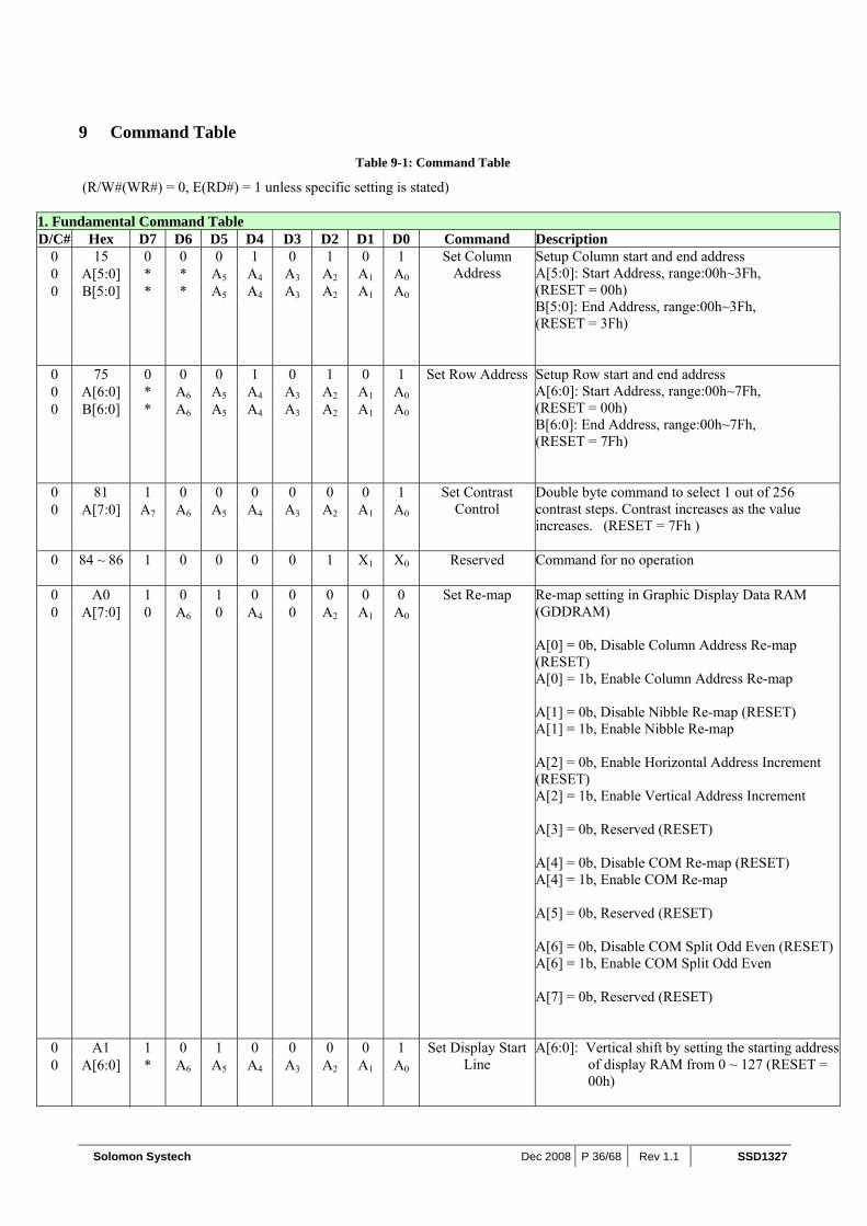
9 Command Table
Table 9-1: Command Table
(R/W#(WR#) = 0, E(RD#) = 1 unless specific setting is stated)
1. Fundamental Command Table D/C# Hex D7 D6 D5 D4 D3 D2 D1 D0 Command Description
0 15 0 0 0 1 0 1 0 1 0 A[5:0] * * A5 A4 A3 A2 A1 A00 B[5:0] * * A5 A4 A3 A2 A1 A0
Set Column Address
Setup Column start and end address A[5:0]: Start Address, range:00h~3Fh, (RESET = 00h) B[5:0]: End Address, range:00h~3Fh, (RESET = 3Fh)
0 75 0 0 0 1 0 1 0 1 0 A[6:0] * A6 A5 A4 A3 A2 A1 A00 B[6:0] * A6 A5 A4 A3 A2 A1 A0
Set Row Address Setup Row start and end address A[6:0]: Start Address, range:00h~7Fh, (RESET = 00h) B[6:0]: End Address, range:00h~7Fh, (RESET = 7Fh)
0 81 1 0 0 0 0 0 0 1 0 A[7:0] A7 A6 A5 A4 A3 A2 A1 A0
Set Contrast Control
Double byte command to select 1 out of 256 contrast steps. Contrast increases as the value increases. (RESET = 7Fh )
0 84 ~ 86 1 0 0 0 0 1 X1 X0
Reserved Command for no operation
0 A0 1 0 1 0 0 0 0 0 0 A[7:0] 0 A6 0 A4 0 A2 A1 A0
Set Re-map Re-map setting in Graphic Display Data RAM (GDDRAM) A[0] = 0b, Disable Column Address Re-map (RESET) A[0] = 1b, Enable Column Address Re-map A[1] = 0b, Disable Nibble Re-map (RESET) A[1] = 1b, Enable Nibble Re-map A[2] = 0b, Enable Horizontal Address Increment (RESET) A[2] = 1b, Enable Vertical Address Increment A[3] = 0b, Reserved (RESET) A[4] = 0b, Disable COM Re-map (RESET) A[4] = 1b, Enable COM Re-map A[5] = 0b, Reserved (RESET) A[6] = 0b, Disable COM Split Odd Even (RESET)A[6] = 1b, Enable COM Split Odd Even A[7] = 0b, Reserved (RESET)
0 A1 1 0 1 0 0 0 0 1 0 A[6:0] * A6 A5 A4 A3 A2 A1 A0
Set Display Start Line
A[6:0]: Vertical shift by setting the starting address of display RAM from 0 ~ 127 (RESET = 00h)
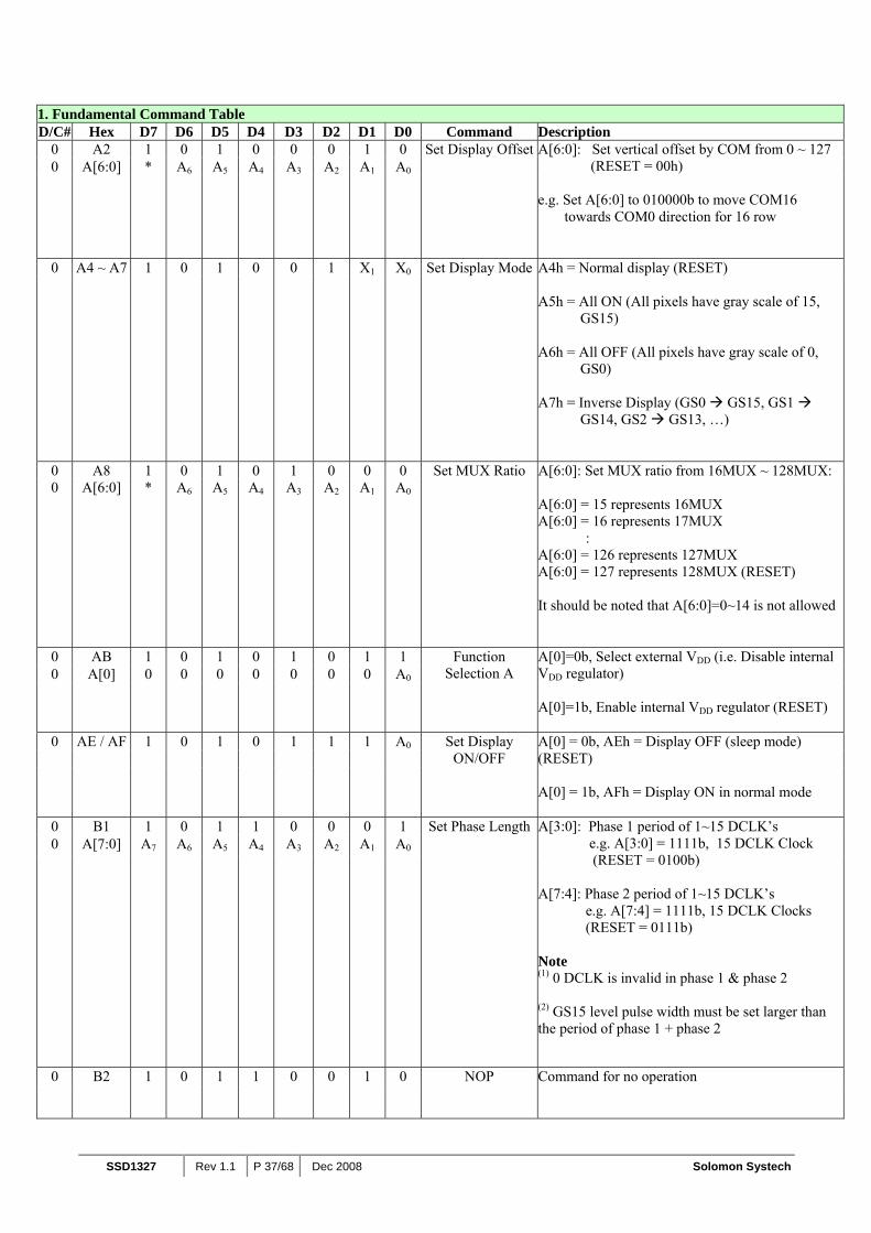
SSD1327 Rev 1.1 P 37/68 Dec 2008 Solomon Systech
1. Fundamental Command Table D/C# Hex D7 D6 D5 D4 D3 D2 D1 D0 Command Description
0 A2 1 0 1 0 0 0 1 0 0 A[6:0] * A6 A5 A4 A3 A2 A1 A0
Set Display Offset A[6:0]: Set vertical offset by COM from 0 ~ 127 (RESET = 00h)
e.g. Set A[6:0] to 010000b to move COM16
towards COM0 direction for 16 row
0 A4 ~ A7 1 0 1 0 0 1 X1 X0
Set Display Mode A4h = Normal display (RESET) A5h = All ON (All pixels have gray scale of 15,
GS15) A6h = All OFF (All pixels have gray scale of 0,
GS0) A7h = Inverse Display (GS0 GS15, GS1
GS14, GS2 GS13, …)
0 A8 1 0 1 0 1 0 0 0 0 A[6:0] * A6 A5 A4 A3 A2 A1 A0
Set MUX Ratio A[6:0]: Set MUX ratio from 16MUX ~ 128MUX: A[6:0] = 15 represents 16MUX A[6:0] = 16 represents 17MUX : A[6:0] = 126 represents 127MUX A[6:0] = 127 represents 128MUX (RESET) It should be noted that A[6:0]=0~14 is not allowed
0 AB 1 0 1 0 1 0 1 1 0 A[0] 0 0 0 0 0 0 0 A0
Function Selection A
A[0]=0b, Select external VDD (i.e. Disable internal VDD regulator) A[0]=1b, Enable internal VDD regulator (RESET)
0 AE / AF 1 0 1 0 1 1 1 A0
Set Display ON/OFF
A[0] = 0b, AEh = Display OFF (sleep mode) (RESET) A[0] = 1b, AFh = Display ON in normal mode
0 B1 1 0 1 1 0 0 0 1 0 A[7:0] A7 A6 A5 A4 A3 A2 A1 A0
Set Phase Length A[3:0]: Phase 1 period of 1~15 DCLK’s e.g. A[3:0] = 1111b, 15 DCLK Clock (RESET = 0100b) A[7:4]: Phase 2 period of 1~15 DCLK’s e.g. A[7:4] = 1111b, 15 DCLK Clocks (RESET = 0111b) Note (1) 0 DCLK is invalid in phase 1 & phase 2 (2) GS15 level pulse width must be set larger than the period of phase 1 + phase 2
0 B2 1 0 1 1 0 0 1 0
NOP Command for no operation

Solomon Systech Dec 2008 P 38/68 Rev 1.1 SSD1327
1. Fundamental Command Table D/C# Hex D7 D6 D5 D4 D3 D2 D1 D0 Command Description
0 B3 1 0 1 1 0 0 1 1 0 A[7:0] A7 A6 A5 A4 A3 A2 A1 A0
Set Front Clock Divider /Oscillator
Frequency
A[3:0]: Define divide ratio (D) of display clock (DCLK) Divide ratio=A[3:0]+1 (RESET is 0000b, i.e. divide ratio = 1)
A[7:4]: Set the Oscillator Frequency, FOSC.
Oscillator Frequency increases with the value of A[7:4] and vice versa. (Range:0000b~1111b)
(RESET = 0000b)
0 B5 1 0 1 1 0 1 0 1 0 A[1:0] 0 0 0 0 0 0 A1 A0
GPIO A[1:0] = 00b represents GPIO pin HiZ, input disable (always read as low)
A[1:0] = 01b represents GPIO pin HiZ, input enable
A[1:0] = 10b represents GPIO pin output Low (RESET)
A[1:0] = 11b represents GPIO pin output High
0 B6 1 0 1 1 0 1 1 0 0 A[3:0] * * * * A3 A2 A1 A0
Set Second pre-charge Period
A[3:0]: Second Pre-charge period of 1~15 DCLK’s e.g. A[3:0] = 1111b, 15 DCLK Clock (RESET = 0100b) Note (1] This command is used to adjust the second pre-charge period after enabling the second pre-charge by setting A[1] = 1b in command D5h
0 B8 1 0 1 1 1 0 0 0 0 A1[5:0] * * A15 A14 A13 A12 A11 A10
0 A2[5:0] * * A25 A24 A23 A22 A21 A20
… … ... ... ... ... ... ... ... ...… … ... ... ... ... ... ... ... ...… … ... ... ... ... ... ... ... ...0 A14[5:0] * * A145 A144 A143 A142 A141 A140
0 A15[5:0] * * A155 A154 A153 A152 A151 A150
Set Gray Scale Table
The next 15 data bytes set the gray scale pulse width in unit of DCLK’s. A1[5:0], value for GS1 level Pulse width A2[5:0], value for GS2 level Pulse width … A14[5:0], value for GS14 level Pulse width A15[5:0], value for GS15 level Pulse width Note (1] The pulse width value of GS1, GS2, .... , GS15 should not be equal. i.e. 0<GS1<GS2 … <GS15 (2) GS15 level pulse width must be set larger than the period of phase 1 + phase 2
0 B9 1 0 1 1 1 0 0 1 Linear LUT
The default Linear Gray Scale table is set in unit of DCLK’s as follow GS0 level pulse width = 0; GS1 level pulse width = 0; GS2 level pulse width = 2; GS3 level pulse width = 4; : : GS14 level pulse width = 26; GS15 level pulse width = 28

SSD1327 Rev 1.1 P 39/68 Dec 2008 Solomon Systech
1. Fundamental Command Table D/C# Hex D7 D6 D5 D4 D3 D2 D1 D0 Command Description
0 BB 1 0 1 1 1 0 1 1
NOP Command for no operation
0 BC 1 0 1 1 1 1 0 0 0 A[3:0] 0 0 0 0 A3 A2 A1 A0
Set Pre-charge voltage
Set pre-charge voltage level.
A[3:0] Hex code
Pre-charge voltage
0000 00h 0.20 x VCC : : : 0101 05h 0.5 x VCC (RESET) : : : 0111 07h 0.613 x VCC 1xxx 08h VCOMH
0 BE 1 0 1 1 1 1 1 0 0 A[2:0] 0 0 0 0 0 A2 A1 A0
Set VCOMH Set COM deselect voltage level.
A[2:0] Hex code V COMH 000 00h 0.72 x VCC
: : : 101 05h 0.82 x VCC (RESET)
: : : 111 07h 0.86 x VCC
0 D5 1 1 0 1 0 1 0 1 0 A[2:0] 0 1 1 0 0 0 A1 A0
Function Selection B
A[1] = 0b: Disable second precharge (RESET) A[1] = 1b: Enable second precharge A[0] = 0b: Internal VSL (RESET) A[0] = 1b: Enable external VSL Note (1) Refer to Table 7-1 for VSL pin details
0 FD 1 1 1 1 1 1 0 1 0 A[2] 0 0 0 1 0 A2 1 0
Set Command Lock
A[2]: MCU protection status. A[2] = 0b, Unlock OLED driver IC MCU interface from entering command (RESET) A[2] = 1b, Lock OLED driver IC MCU interface from entering command Note (1) The locked OLED driver IC MCU interface prohibits all commands and memory access except the FDh command

Solomon Systech Dec 2008 P 40/68 Rev 1.1 SSD1327
2. Scrolling Command Table D/C#Hex D7 D6 D5 D4 D3 D2 D1 D0 Command Description 0 26 / 27 0 0 1 0 0 1 1 X0 0 A[7:0] 0 0 0 0 0 0 0 0 0 B[6:0] * B6 B5 B4 B3 B2 B1 B00 C[2:0] * * * 0 0 C2 C1 C00 D[6:0] * D6 D5 D4 D3 D2 D1 D00 E[5:0] * * E5 E4 E3 E2 E1 E00 F[5:0] * * F5 F4 F3 F2 F1 F00 G[7:0] 0 0 0 0 0 0 0 0
Continuous Horizontal Scroll Setup
26h, X[0]=0, Right Horizontal Scroll 27h, X[0]=1, Left Horizontal Scroll (Horizontal scroll by 1 column) A[7:0] : Dummy byte (Set as 00h) B[2:0] : Define start row address; range:00h~7Fh, (RESET = 00h) C[2:0] : Set time interval between each scroll step in terms
of frame frequency 000b – 6 frames 100b – 3 frames 001b – 32 frames 101b – 4 frames 010b – 64 frames 110b – 5 frame 011b – 256 frames 111b – 2 frame
D[2:0] : Define end row address; range:00h~7Fh, (RESET = 7Fh) The value of D[2:0] must be larger or equal to B[2:0]
E[7:0] : Define start column address; range:00h~3Fh, (RESET = 00h) F[7:0] : Define end column address; range:00h~3Fh, (RESET = 3Fh) The value of F[2:0] must be larger or equal to E[2:0]
G[7:0] : Dummy byte (Set as 00h)
0 2E 0 0 1 0 1 1 1 0
Deactivate scroll Stop scrolling that is configured by command 26h/27h Note (1) After sending 2Eh command to deactivate the scrolling action, the ram data needs to be rewritten.
0 2F 0 0 1 0 1 1 1 1
Activate scroll Start scrolling that is configured by the scrolling setup commands :26h/27h with the following valid sequences: Valid command sequence 1: 26h ;2Fh. Valid command sequence 2: 27h ;2Fh.
Note (1) “*” stands for “Don’t care”.

SSD1327 Rev 1.1 P 41/68 Dec 2008 Solomon Systech
9.1 Data Read / Write To read data from the GDDRAM, select HIGH for both the R/W# (WR#) pin and the D/C# pin for 6800-series parallel mode and select LOW for the E (RD#) pin and HIGH for the D/C# pin for 8080-series parallel mode. No data read is provided in serial mode operation. In normal data read mode the GDDRAM column address pointer will be increased automatically by one after each data read. Also, a dummy read is required before the first data read. To write data to the GDDRAM, select LOW for the R/W# (WR#) pin and HIGH for the D/C# pin for both 6800-series parallel mode and 8080-series parallel mode. The serial interface mode is always in write mode. The GDDRAM column address pointer will be increased automatically by one after each data write.
Table 9-2 : Address increment table (Automatic)
D/C# R/W# (WR#) Comment Address Increment 0 0 Write Command No 0 1 Read Status No 1 0 Write Data Yes 1 1 Read Data Yes

Solomon Systech Dec 2008 P 42/68 Rev 1.1 SSD1327
10 COMMAND DESCRIPTIONS
10.1 Fundamental command description
10.1.1 Set Column Address (15h) This triple byte command specifies column start address and end address of the display data RAM. This command also sets the column address pointer to column start address. This pointer is used to define the current read/write column address in graphic display data RAM. If horizontal address increment mode is enabled by command A0h, after finishing read/write one column data, it is incremented automatically to the next column address. Whenever the column address pointer finishes accessing the end column address, it is reset back to start column address and the row address is incremented to the next row.
10.1.2 Set Row Address (75h) This triple byte command specifies row start address and end address of the display data RAM. This command also sets the row address pointer to row start address. This pointer is used to define the current read/write row address in graphic display data RAM. If vertical address increment mode is enabled by command A0h, after finishing read/write one row data, it is incremented automatically to the next row address. Whenever the row address pointer finishes accessing the end row address, it is reset back to start row address. The diagram below shows the way of column and row address pointer movement through the example: column start address is set to 2 and column end address is set to 61, row start address is set to 1 and row end address is set to 126; horizontal address increment mode is enabled by command A0h. In this case, the graphic display data RAM column accessible range is from column 2 to column 61 and from row 1 to row 126 only. In addition, the column address pointer is set to 2 and row address pointer is set to 1. After finishing read/write one pixel of data, the column address is increased automatically by 1 to access the next RAM location for next read/write operation (solid line in Figure 10-1). Whenever the column address pointer finishes accessing the end column 61, it is reset back to column 2 and row address is automatically increased by 1 (solid line in Figure 10-1). While the end row 126 and end column 61 RAM location is accessed, the row address is reset back to 1 and the column address is reset back to 2 (dotted line in Figure 10-1).
Figure 10-1: Example of Column and Row Address Pointer Movement
0 1 2 ….. ……. 61 62 63 Column address
SEG
0
SEG
1
SEG
2
SEG
3
SEG
4
SEG
5
: : : :
SEG
122
SEG
123
SEG
124
SEG
125
SEG
126
SEG
127 SEG outputs
Row 0 : Row 1 Row 2
: : : :
Row 125 Row 126 Row 127 :

SSD1327 Rev 1.1 P 43/68 Dec 2008 Solomon Systech
10.1.3 Set Contrast Current (81h) This double byte command is used to set Contrast Setting of the display. The chip has 256 contrast steps from 00h to FFh. The segment output current ISEG increases linearly with the contrast step, which results in brighter display.
10.1.4 NOP (84h ~ 86h) These are no operation commands.
10.1.5 Set Re-map (A0h) This double byte command has multiple configurations and each bit setting is described as follows:
• Column Address Remapping (A[0]) This bit is made for increase the flexibility layout of segment signals in OLED module with segment arranged from left to right (when A[0] is set to 0) or from right to left (when A[0] is set to 1).
• Nibble Remapping (A[1]) When A[1] is set to 1, the two nibbles of the data bus for RAM access are re-mapped, such that (D7, D6, D5, D4, D3, D2, D1, D0) acts like (D3, D2, D1, D0, D7, D6, D5, D4). If this feature works together with Column Address Re-map, it would produce an effect of flipping the outputs from SEG0~127 to SEG127~SEG0 as show in Table 8-8.
• Address increment mode (A[2]) When A[2] is set to 0, the driver is set as horizontal address increment mode. After the display RAM is read / written, the column address pointer is increased automatically by 1. If the column address pointer reaches column end address, the column address pointer is reset to column start address and row address pointer is increased by 1. The sequence of movement of the row and column address point for horizontal address increment mode is shown in Figure 10-2.
Figure 10-2: Address Pointer Movement of Horizontal Address Increment Mode
0 1 ….. 62 63 Column address Row 0 Row 1
: : : : : : Row 126 Row 127

Solomon Systech Dec 2008 P 44/68 Rev 1.1 SSD1327
When A[2] is set to 1, the driver is set to vertical address increment mode. After the display RAM is read / written, the row address pointer is increased automatically by 1. If the row address pointer reaches the row end address, the row address pointer is reset to row start address and column address pointer is increased by 1. The sequence of movement of the row and column address point for vertical address increment mode is shown in Figure 10-3.
Figure 10-3: Address Pointer Movement of Vertical Address Increment Mode
0 1 ….. 62 63 Column address Row 0 ….. Row 1 …..
: : Row 126 ….. Row 127 …..
• COM Remapping (A[4]) This bit defines the scanning direction of the common for flexible layout of common signals in OLED module either from up to down (when A[4] is set to 0) or from bottom to up (when A[4] is set to 1). Table 8-9 shows an example of the using the COM Remapping to perform vertical scrolling.
• Splitting of Odd / Even COM Signals (A[6]) This bit is made to match the COM layout connection on the panel.
When A[6] is set to 0, no splitting odd / even of the COM signal is performed, output pin assignment sequence is shown as below (for 128MUX ratio):
Figure 10-4: Output pin assignment when command A0h bit A[6]=0.
128 x 128
ROW0
ROW63ROW64
ROW127
Pad 1,2,3,… Gold Bumps face up
SSD1327Z
COM0
COM64
COM127 COM63
Output Pin Connection SSD1327Z Panel
COM0 ROW0 COM1 ROW1 COM2 ROW2 COM3 ROW3
: : COM63 ROW63 COM64 ROW64
: : COM125 ROW125 COM126 ROW126 COM127 ROW127
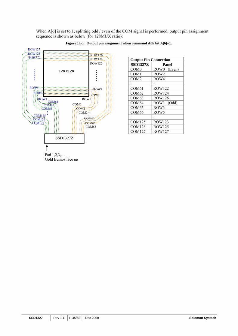
SSD1327 Rev 1.1 P 45/68 Dec 2008 Solomon Systech
When A[6] is set to 1, splitting odd / even of the COM signal is performed, output pin assignment sequence is shown as below (for 128MUX ratio):
Figure 10-5 : Output pin assignment when command A0h bit A[6]=1.
128 x128
ROW0
ROW126
ROW127
SSD1327Z
COM0 COM64
COM127 COM63
ROW1
Pad 1,2,3,… Gold Bumps face up
......
......
COM2
COM61
ROW4
ROW122ROW124
ROW2
COM1
COM62
ROW125 ROW123
COM66 COM65
COM126 COM125
ROW3 ROW5
... ...
Output Pin Connection SSD1327Z Panel COM0 ROW0 (Even) COM1 ROW2 COM2 ROW4 : : COM61 ROW122 COM62 ROW124 COM63 ROW126 COM64 ROW1 (Odd) COM65 ROW3 COM66 ROW5 : : COM125 ROW123 COM126 ROW125 COM127 ROW127
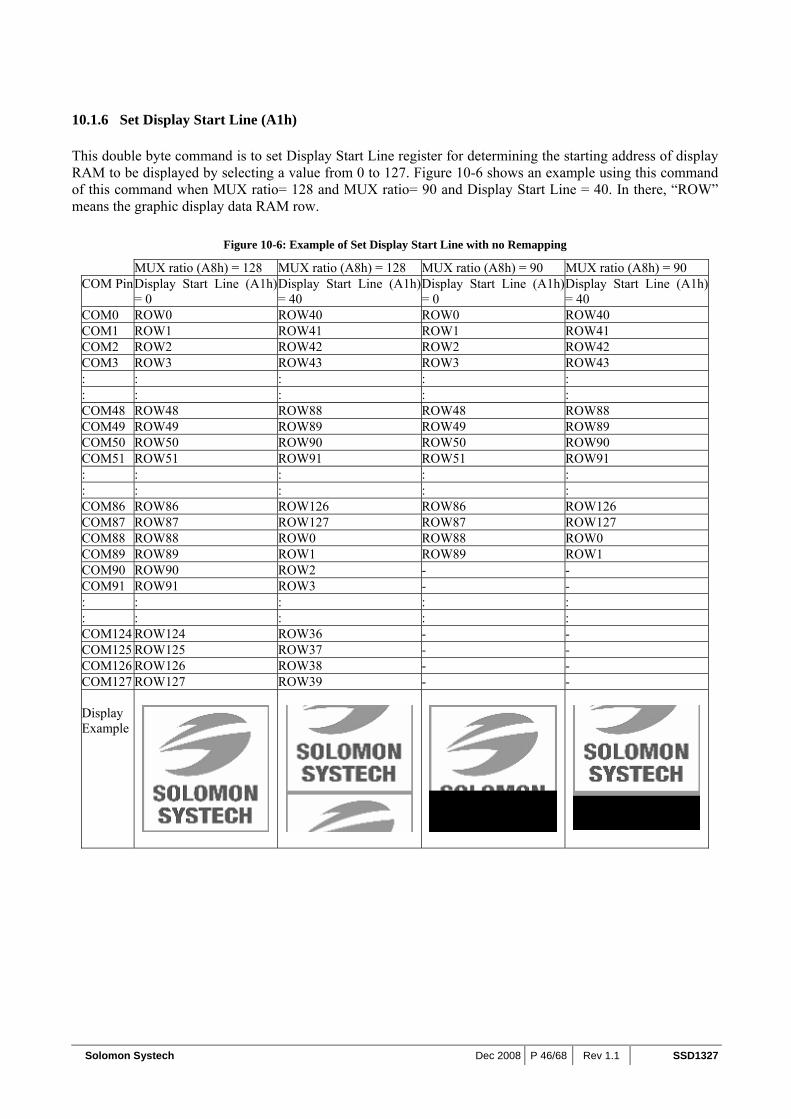
Solomon Systech Dec 2008 P 46/68 Rev 1.1 SSD1327
10.1.6 Set Display Start Line (A1h) This double byte command is to set Display Start Line register for determining the starting address of display RAM to be displayed by selecting a value from 0 to 127. Figure 10-6 shows an example using this command of this command when MUX ratio= 128 and MUX ratio= 90 and Display Start Line = 40. In there, “ROW” means the graphic display data RAM row.
Figure 10-6: Example of Set Display Start Line with no Remapping
MUX ratio (A8h) = 128 MUX ratio (A8h) = 128 MUX ratio (A8h) = 90 MUX ratio (A8h) = 90 COM Pin Display Start Line (A1h)
= 0 Display Start Line (A1h)= 40
Display Start Line (A1h) = 0
Display Start Line (A1h) = 40
COM0 ROW0 ROW40 ROW0 ROW40 COM1 ROW1 ROW41 ROW1 ROW41 COM2 ROW2 ROW42 ROW2 ROW42 COM3 ROW3 ROW43 ROW3 ROW43 : : : : : : : : : : COM48 ROW48 ROW88 ROW48 ROW88 COM49 ROW49 ROW89 ROW49 ROW89 COM50 ROW50 ROW90 ROW50 ROW90 COM51 ROW51 ROW91 ROW51 ROW91 : : : : : : : : : : COM86 ROW86 ROW126 ROW86 ROW126 COM87 ROW87 ROW127 ROW87 ROW127 COM88 ROW88 ROW0 ROW88 ROW0 COM89 ROW89 ROW1 ROW89 ROW1 COM90 ROW90 ROW2 - - COM91 ROW91 ROW3 - - : : : : : : : : : : COM124 ROW124 ROW36 - - COM125 ROW125 ROW37 - - COM126 ROW126 ROW38 - - COM127 ROW127 ROW39 - - Display Example
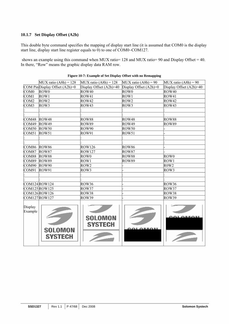
SSD1327 Rev 1.1 P 47/68 Dec 2008 Solomon Systech
10.1.7 Set Display Offset (A2h) This double byte command specifies the mapping of display start line (it is assumed that COM0 is the display start line, display start line register equals to 0) to one of COM0~COM127. shows an example using this command when MUX ratio= 128 and MUX ratio= 90 and Display Offset = 40. In there, “Row” means the graphic display data RAM row.
Figure 10-7: Example of Set Display Offset with no Remapping
MUX ratio (A8h) = 128 MUX ratio (A8h) = 128 MUX ratio (A8h) = 90 MUX ratio (A8h) = 90 COM Pin Display Offset (A2h)=0 Display Offset (A2h)=40 Display Offset (A2h)=0 Display Offset (A2h)=40COM0 ROW0 ROW40 ROW0 ROW40 COM1 ROW1 ROW41 ROW1 ROW41 COM2 ROW2 ROW42 ROW2 ROW42 COM3 ROW3 ROW43 ROW3 ROW43 : : : : : : : : : : COM48 ROW48 ROW88 ROW48 ROW88 COM49 ROW49 ROW89 ROW49 ROW89 COM50 ROW50 ROW90 ROW50 - COM51 ROW51 ROW91 ROW51 - : : : : : : : : : : COM86 ROW86 ROW126 ROW86 - COM87 ROW87 ROW127 ROW87 - COM88 ROW88 ROW0 ROW88 ROW0 COM89 ROW89 ROW1 ROW89 ROW1 COM90 ROW90 ROW2 - R0W2 COM91 ROW91 ROW3 - ROW3 : : : : : : : : : : COM124 ROW124 ROW36 - ROW36 COM125 ROW125 ROW37 - ROW37 COM126 ROW126 ROW38 - ROW38 COM127 ROW127 ROW39 - ROW39 Display Example

Solomon Systech Dec 2008 P 48/68 Rev 1.1 SSD1327
10.1.8 Set Display Mode (A4h ~ A7h) These are single byte commands (A4h ~ A7h) and are used to set display status to Normal Display, Entire Display ON, Entire Display OFF or Inverse Display, respectively.
• Normal Display (A4h) Reset the “Entire Display ON, Entire Display OFF or Inverse Display” effects and turn the data to ON at the corresponding gray level. Figure 10-8 shows an example of Normal Display.
Figure 10-8: Example of Normal Display
Memory Display
• Set Entire Display ON (A5h)
Force the entire display to be at gray scale level GS15, regardless of the contents of the display data RAM, as shown on Figure 10-9.
Figure 10-9: Example of Entire Display ON
Memory Display
• Set Entire Display OFF (A6h)
Force the entire display to be at gray scale level GS0, regardless of the contents of the display data RAM, as shown on Figure 10-10.
Figure 10-10 : Example of Entire Display OFF
Memory Display
• Inverse Display (A7h)
The gray scale level of display data are swapped such that “GS0” <-> “GS15”, “GS1” <-> “GS14”, etc. Figure 10-11 shows an example of inverse display.
Figure 10-11: Example of Inverse Display
Memory Display

SSD1327 Rev 1.1 P 49/68 Dec 2008 Solomon Systech
10.1.9 Set Multiplex Ratio (A8h) This double byte command sets multiplex ratio (MUX ratio) from 16MUX to 128MUX. In RESET, multiplex ratio is 128MUX. Please refer to Figure 10-6 and Figure 10-7 for the example of setting different MUX ratio.
10.1.10 Function selection A (ABh) This double byte command is used to enable or disable the VDD regulator. Internal VDD regulator is enabled when the bit A[0] is set to 1b, while internal VDD regulator is disabled when A[0] is set to 0b.
10.1.11 Set Display ON/OFF (AEh / AFh) These single byte commands are used to turn the OLED panel display ON or OFF. When the display is OFF (command AEh), the segment pins are in VSS state and common pins are in high impedance state.
Figure 10-12: Display ON Sequence (when initial start)
Power supply setting (1) Send command AFh to turn the panel display ON (2) Display on and start to write RAM
Figure 10-13: Display OFF Sequence
Display on (2) Send command AEh to turn the panel display OFF (2) Display off at Sleep mode (3) Set command ABh to 00h to disable
the internal VDD regulator (3) (4)
Note: (1) Please follow the power ON sequence as suggested on Figure 8-17 (2) Internal VDD regulator is ON as default (3) The RAM content is kept during display off at both sleep mode and the case that internal VDD regulator is disabled. (4) It is recommended to disable internal VDD regulator during Sleep mode for power save. Refer to Table 12-1.
Solomon Systech Dec 2008 P 50/68 Rev 1.1 SSD1327
Figure 10-14: Display ON Sequence (During Sleep mode and internal VDD regulator is disabled)
Display off at Sleep mode and internal VDD regulator is disabled (1) Set command ABh to 01h to enable the internal VDD regulator Send command AFh to turn the panel display ON
Display on and start to write RAM Note: (1) The RAM content is kept during display off at sleep mode and internal VDD regulator is disabled.
10.1.12 Set Phase Length (B1h) This double byte command sets the length of phase 1 and 2 of segment waveform of the driver.
• Phase 1 (A[3:0]): Set the period from 1 to 15 in the unit of DCLKs. A larger capacitance of the OLED pixel may require longer period to discharge the previous data charge completely.
• Phase 2 (A[7:4]): Set the period from 1 to 15 in the unit of DCLKs. A longer period is needed to
charge up a larger capacitance of the OLED pixel to the target voltage VP.
10.1.13 NOP (B2h) These are no operation commands.
10.1.14 Set Front Clock Divider / Oscillator Frequency (B3h) This double byte command consists of two functions:
• Front Clock Divide Ratio (A[3:0]) Set the divide ratio to generate DCLK (Display Clock) from CLK. The divide ratio is from 1 to 16, with reset value = 1. Please refer to Section 8.3 for the detail relationship of DCLK and CLK.
• Oscillator Frequency (A[7:4]) Program the oscillator frequency Fosc which is the source of CLK if CLS pin is pulled HIGH. The 4-bit value results in 16 different frequency settings being available.
10.1.15 Set GPIO (B5h) This double byte command is used to set the states of GPIO0 and GPIO1 pins. Refer to Table 9-1 for details.

SSD1327 Rev 1.1 P 51/68 Dec 2008 Solomon Systech
10.1.16 Set Second Pre-charge period (B6h) This double byte command is used to set the phase 3 second pre-charge period. The period of phase 3 can be programmed by command B6h and it is ranged from 0 to 15 DCLK's (as long as the second pre-charge is enabled by setting A[1] of command D5h to 1). Please refer to Table 9-1 for the detail information.
10.1.17 Set Gray Scale Table (B8h) This command is used to set each individual gray scale level for the display. Except gray scale levels GS0 that has no pre-charge and current drive, each gray scale level is programmed in the length of current drive stage pulse width with unit of DCLK. The longer the length of the pulse width, the brighter the OLED pixel when it’s turned ON. Following the command B8h, the user has to set the gray scale setting for GS1, GS2, …, GS14, GS15 one by one in sequence. Refer to Section 8.8 for details. The setting of gray scale table entry can perform gamma correction on OLED panel display. Since the perception of the brightness scale shall match the image data value in display data RAM, appropriate gray scale table setting like the example shown below (Figure 10-15) can compensate this effect.
Figure 10-15 : Example of Gamma correction by Gamma Look Up table setting
10.1.18 Select Default Linear Gray Scale Table (B9h) This single byte command reloads the preset linear Gray Scale table as GS0 =Gamma Setting 0, GS1 = Gamma Setting 0, GS2 = Gamma Setting 2, ..., GS14 = Gamma Setting 26, GS15 = Gamma Setting 28. Refer to Section 8.8 for details.
10.1.19 NOP (BBh) These are no operation commands.
10.1.20 Set Pre-charge voltage (BCh) This double byte command sets the first pre-charge voltage (phase 2) level of segment pins. The level of pre-charge voltage is programmed with reference to VCC. Refer to Table 9-1 for details.
10.1.21 Set VCOMH Voltage (BEh) This double byte command sets the high voltage level of common pins, VCOMH. The level of VCOMH is programmed with reference to VCC. Refer to Table 9-1 for details.
Gamma Setting
Gray Scale Table
Panel response
Brightness Brightness
Gamma Setting Gray Scale Table
Gamma Look Up table setting
Result in linear response

Solomon Systech Dec 2008 P 52/68 Rev 1.1 SSD1327
10.1.22 Function selection B (D5h) This double byte command consists of two functions:
• Set second precharge (A[1]) Second precharge is enabled when A[1] is set to 1, whereas it is disabled as default at A[1] = 0. .
• Set VSL (A[0]) External VSL is enabled when A[0] is set to 1, whereas it is set to internal VSL as default at A[0] = 0. Refer to Table 9-1 for details.
10.1.23 Set Command Lock (FDh) This double byte command is used to lock the OLED driver IC from accepting any command except itself. After entering FDh 16h (A[2]=1b), the OLED driver IC will not respond to any newly-entered command (except FDh 12h A[2]=0b) and there will be no memory access. This is call “Lock” state. That means the OLED driver IC ignore all the commands (except FDh 12h A[2]=0b) during the “Lock” state. Entering FDh 12h (A[2]=0b) can unlock the OLED driver IC. That means the driver IC resume from the “Lock” state. And the driver IC will then respond to the command and memory access.

SSD1327 Rev 1.1 P 53/68 Dec 2008 Solomon Systech
10.2 Graphic Acceleration command description
10.2.1 Horizontal Scroll Setup (26h/27h) This command consists of consecutive bytes to set up the horizontal scroll parameters and determines the scrolling start page, end page and scrolling speed. Before issuing this command the horizontal scroll must be deactivated (2Eh). Otherwise, RAM content may be corrupted. The SSD1327 horizontal scroll is designed for 128 columns scrolling. The following two figures (Figure 10-16, Figure 10-17, and Figure 10-18) show the examples of using the horizontal scroll:
Figure 10-16 : Horizontal scroll example: Scroll RIGHT by 1 column
Original Setting SEG
0
SEG
1
SEG
2
SEG
3
SEG
4
SEG
5 …
…
…
SEG
122
SEG
123
SEG
124
SEG
125
SEG
126
SEG
127
After one scroll step
SEG
127
SEG
0
SEG
1
SEG
2
SEG
3
SEG
4
…
…
…
SEG
121
SEG
122
SEG
123
SEG
124
SEG
125
SEG
126
Figure 10-17 : Horizontal scroll example: Scroll LEFT by 1 column
Original Setting SE
G0
SEG
1
SEG
2
SEG
3
SEG
4
SEG
5 …
…
…
SEG
122
SEG
123
SEG
124
SEG
125
SEG
126
SEG
127
After one scroll step SE
G1
SEG
2
SEG
3
SEG
4
SEG
5
SEG
6 …
…
…
SEG
123
SEG
124
SEG
125
SEG
126
SEG
127
SEG
0
Figure 10-18 : Horizontal scrolling setup example

Solomon Systech Dec 2008 P 54/68 Rev 1.1 SSD1327
10.2.2 Deactivate Scroll (2Eh) This command stops the motion of scrolling. After sending 2Eh command to deactivate the scrolling action, the ram data needs to be rewritten.
10.2.3 Activate Scroll (2Fh) This command starts the motion of scrolling and should only be issued after the scroll setup parameters have been defined by the scrolling setup commands: 26h / 27h. The setting in the latest scrolling setup command overwrites the setting in the previous scrolling setup command. The following actions are prohibited after the scrolling is activated,
1. RAM access (Data write or read). 2. Changing the horizontal scroll setup parameters.

SSD1327 Rev 1.1 P 55/68 Dec 2008 Solomon Systech
11 MAXIMUM RATINGS
Table 11-1: Maximum Ratings
(Voltage Reference to VSS) Symbol Parameter Value Unit
VDD -0.5 to 2.75 V VCC -0.5 to 19.0 V VCI
Supply Voltage -0.3 to 4.0 V
VSEG SEG output voltage 0 to VCC V VCOM COM output voltage 0 to 0.9*VCC V
Vin Input voltage Vss-0.3 to VCI+0.3 V TA Operating Temperature -40 to +85 ºC Tstg Storage Temperature Range -65 to +150 ºC
*Maximum Ratings are those values beyond which damage to the device may occur. Functional operation should be restricted to the limits in the Electrical Characteristics tables or Pin Description. *This device may be light sensitive. Caution should be taken to avoid exposure of this device to any light source during normal operation. This device is not radiation protected.

Solomon Systech Dec 2008 P 56/68 Rev 1.1 SSD1327
12 DC CHARACTERISTICS Conditions (Unless otherwise specified):
Voltage referenced to VSS VDD = 1.65 to 2.6V VCI = 1.65 to 3.5V (VCI must be larger than or equal to VDD) TA = 25°C
Table 12-1 : DC Characteristics
Symbol Parameter Test Condition Min. Typ. Max. UnitVCC Operating Voltage - 8 - 18 V VDD Logic Supply Voltage - 1.65 - 2.6 V
VCI Low voltage power supply, power supply for I/O pins - 1.65 - 3.5 V
VOH High Logic Output Level Iout = 100uA 0.9*VCI - VCI V VOL Low Logic Output Level Iout = 100uA 0 - 0.1*VCI V VIH (1) High Logic Input Level - 0.8*VCI - VCI V VIL (1) Low Logic Input Level - 0 - 0.2*VCI V
ISLP_VDD VDD Sleep mode Current VCI = 2.8V, VCC =OFF VDD(external) = 2.5V, Display OFF, No panel attached
- - 10 uA
External VDD = 2.5V - - 10 uA
Enable Internal VDD during Sleep mode
- - 40 uA ISLP_VCI VCI Sleep mode Current
VCI = 2.8V, VCC =OFF Display OFF, No panel attached Disable Internal VDD
during Sleep mode (Deep Sleep mode)
- - 10 uA
ISLP_VCC VCC Sleep mode Current VCI = 2.8V, VCC = 8~18V VDD(external) = 2.5V, Display OFF, No panel attached
- - 10 uA
IDD VDD Supply Current VCI = 3.5V, VCC = 18V, External VDD = 2.5V, Display ON, No panel attached, contrast = FF
- 22 - uA
External VDD = 2.5V - 35 50 uA
ICI VCI Supply Current VCI = 3.5V, VCC = 18V, Display ON, No panel attached, contrast = FF Internal VDD
= 2.5V - 95 120 uA
External VDD = 2.5V - 600 750 uA
ICC VCC Supply Current VCI = 3.5V, VCC = 18V, Display ON, No panel attached, contrast = FF Internal VDD
= 2.5V - 600 750 uA
Contrast = FF - 300 370 uAContrast = AF - 206 - uAContrast = 7F - 150 - uAContrast = 3F - 75 - uA
ISEG Segment Output Current Setting VCC=18V, IREF=10uA
Contrast = 1F - 37.5 - uA
Dev Segment output current uniformity
Dev = (ISEG – IMID) / IMID IMID = (IMAX + IMIN) / 2 ISEG = Segment current at contrast FF
-3 - 3 %
Adj. Dev Adjacent pin output current uniformity (contrast = FFh)
Adj Dev = ( I[n]-I[n+1] ) / (I[n]+I[n+1]) -2 - 2 %

SSD1327 Rev 1.1 P 57/68 Dec 2008 Solomon Systech
13 AC CHARACTERISTICS Conditions:
Voltage referenced to VSS VDD = 2.4 to2.6V TA = 25°C
Table 13-1 : AC Characteristics
Symbol Parameter Test Condition Min. Typ. Max. Unit
FOSC (1) Oscillation Frequency of Display Timing Generator
VCI = 2.8V, internal VDD 535 595 655 kHz
FFRM Frame Frequency for 128 MUX Mode
128x128 Graphic Display Mode, Display ON, Internal Oscillator Enabled
- FOSC * 1 / (D * K * 128)(2) - Hz
tRES Reset low pulse width (RES#) - 2000 - - ns Note (1) FOSC stands for the frequency value of the internal oscillator and the value is measured when command B3h A[7:4] is in default value. (2) D: divide ratio K: Phase 1 period + Phase 2 period + X X: DCLKs in current drive period.
Default K is 4 + 7 + 30 = 41
Solomon Systech Dec 2008 P 58/68 Rev 1.1 SSD1327
Table 13-2 : 6800-Series MCU Parallel Interface Timing Characteristics
(VCI - VSS = 1.65V to 3.5V, TA = 25°C) Symbol Parameter Min Typ Max Unit tcycle Clock Cycle Time 300 - - ns tAS Address Setup Time 10 - - ns tAH Address Hold Time 0 - - ns tDSW Write Data Setup Time 40 - - ns tDHW Write Data Hold Time 7 - - ns tDHR Read Data Hold Time 20 - - ns tOH Output Disable Time - - 70 ns tACC Access Time - - 140 ns
PWCSL Chip Select Low Pulse Width (read) Chip Select Low Pulse Width (write)
120 60 - - ns
PWCSH Chip Select High Pulse Width (read) Chip Select High Pulse Width (write)
60 60 - - ns
tR Rise Time - - 15 ns tF Fall Time - - 15 ns
Figure 13-1 : 6800-series MCU parallel interface characteristics
D[7:0] (WRITE)
D[7:0] (READ)
E(RD#)
CS#
R/W#(WR#) #
PWCSL
tR
t F tDHW
tOH
t ACC tDHR
Valid Data
tDSW
Valid Data
tcyclePWCSH
tAHt AS
D/C #

SSD1327 Rev 1.1 P 59/68 Dec 2008 Solomon Systech
Table 13-3 : 8080-Series MCU Parallel Interface Timing Characteristics
(VCI - VSS = 1.65V to 3.5V, TA = 25°C) Symbol Parameter Min Typ Max Unittcycle Clock Cycle Time 300 - - ns tAS Address Setup Time 10 - - ns tAH Address Hold Time 0 - - ns tDSW Write Data Setup Time 40 - - ns tDHW Write Data Hold Time 7 - - ns tDHR Read Data Hold Time 20 - - ns tOH Output Disable Time - - 70 ns tACC Access Time - - 140 ns tPWLR Read Low Time 150 - - ns tPWLW Write Low Time 60 - - ns tPWHR Read High Time 60 - - ns tPWHW Write High Time 60 - - ns tR Rise Time - - 15 ns tF Fall Time - - 15 ns tCS Chip select setup time 0 - - ns tCSH Chip select hold time to read signal 0 - - ns tCSF Chip select hold time 20 - - ns
Figure 13-2 : 8080-series MCU parallel interface characteristics
D[7:0]
Write cycle Read cycle
R/W#(WR#)
t AS
D/C#
CS# t CS
t AH
t PWLW
t cycle
t DSW t DHW
t PWHW
tCSF
E(RD#)
tAS
D/C#
CS#
tCS
t AH
t PWLR t cycle
t PWHR
t CSH
tACC t DHR
t OH
t F tR tF t R
D[7:0]

Solomon Systech Dec 2008 P 60/68 Rev 1.1 SSD1327
Table 13-4 : Serial Interface Timing Characteristics (4-wire SPI)
(VCI - VSS = 1.65V to 3.5V, TA = 25°C) Symbol Parameter Min Typ Max Unit tcycle Clock Cycle Time 100 - - ns tAS Address Setup Time 15 - - ns tAH Address Hold Time 15 - - ns tCSS Chip Select Setup Time 20 - - ns tCSH Chip Select Hold Time 10 - - ns tDSW Write Data Setup Time 15 - - ns tDHW Write Data Hold Time 15 - - ns tCLKL Clock Low Time 20 - - ns tCLKH Clock High Time 20 - - ns tR Rise Time - - 15 ns tF Fall Time - - 15 ns
Figure 13-3 : Serial interface characteristics (4-wire SPI)
t AHtAS
D/C#
Valid Data
tDHW
t CLKL
tDSW
t CLKH tcycle
t CSS tCSH
t F tR
SDIN (D1)
CS#
SCLK (D0)
D7 SDIN(D1)
CS#
SCLK (D0)
D6 D5 D4 D3 D2 D1 D0

SSD1327 Rev 1.1 P 61/68 Dec 2008 Solomon Systech
Table 13-5: Serial Interface Timing Characteristics (3-wire SPI)
(VCI - VSS = 1.65V to 3.5V, TA = 25°C) Symbol Parameter Min Typ Max Unit tcycle Clock Cycle Time 100 - - ns tCSS Chip Select Setup Time 20 - - ns tCSH Chip Select Hold Time 10 - - ns tDSW Write Data Setup Time 15 - - ns tDHW Write Data Hold Time 15 - - ns tCLKL Clock Low Time 20 - - ns tCLKH Clock High Time 20 - - ns tR Rise Time - - 15 ns tF Fall Time - - 15 ns
Figure 13-4: Serial interface characteristics (3-wire SPI)
SDIN (D1)
CS#
SCLK (D0)
D7 D6 D5 D4 D3 D2 D1 D0 D/C#
Valid Data
tDHW
t CLKL
t DSW
tCLKH tCYCLE
t CSS tCSH
t F tR
SDIN (D1)
CS#
SCLK (D0)

Solomon Systech Dec 2008 P 62/68 Rev 1.1 SSD1327
Table 13-6: I2C Interface Timing Characteristics
(VCI - VSS = 1.65V to 3.5V, TA = 25°C) Symbol Parameter Min Typ Max Unit
tcycle Clock Cycle Time 2.5 - - us
tHSTART Start condition Hold Time 0.6 - - us
Data Hold Time (for “SDAOUT” pin) 0 - - ns tHD
Data Hold Time (for “SDAIN” pin) 300 - - ns
tSD Data Setup Time 100 - - ns
tSSTART Start condition Setup Time (Only relevant for a repeated Start condition)
0.6 - - us
tSSTOP Stop condition Setup Time 0.6 - - us
tR Rise Time for data and clock pin - - 300 ns
tF Fall Time for data and clock pin - - 300 ns
tIDLE Idle Time before a new transmission can start 1.3 - - us
Figure 13-5: I2C interface Timing characteristics
// //
SDA
SCL
tHSTART
tCYCLE
tHD
tR
tF tSD
tSSTART tSSTOP
tIDLE
SSD1327 Rev 1.1 P 63/68 Dec 2008 Solomon Systech
14 APPLICATION EXAMPLES
Figure 14-1 : SSD1327Z application example for 8-bit 6800-parallel interface mode (Internal regulated VDD)
The configuration for 8-bit 6800-parallel interface mode, externally VCC is shown in the following diagram: (VCI =2.8V (VCI must be > 2.6V), Internal regulated VDD = 2.5V, external VCC = 15V, IREF = 10uA)
Voltage at IREF ≈ VCC – 3V. For VCC = 15V, IREF = 10uA: R1 = (Voltage at IREF - VSS) / IREF
≈ (15 - 3)V / 10uA = 1.2MΩ C1 = C2: 1uF (1), C3 = C4: 4.7uF (1) Pin connected to MCU interface: D0~D7, E, R/W#, D/C#, CS#, RES# Pin internally connected to VCI: CLS, BS2 Pin internally connected to VSS: VLSS, BGGND, CL, BS1, BS0 Pin floated: GPIO (2), VSL (2), FR Note (1) The value is recommended value. Select appropriate value against module application. (2) Depends on module application. (3) Die gold bump face up. (4) VLSS of IC pad no. 29 to 85 are recommended to be connected to the VLSS of pad no. 28 and 86 to form a larger area of GND. (5) VLSS and VSS are not recommended to be connected on the ITO routing, but connected together in the PCB level for better grounding and noise insulation.
OLED Panel 128x128
CO
M12
7 : : :
CO
M1
SEG
127
SEG
126
: : : : : : : : : SE
G1
SEG
0 C
OM
0 : : : C
OM
126
C2
SSD1327Z
VSL
V
CC
VC
OM
H
GPI
O
VC
I V
DD
I REF
C
S#
RES
# D
/C#
R/W
# (W
R#)
E
(RD
#)
D[0
:7]
VSS
V
LSS
C4
R1
C1
C3
C
S#
RES
# D
/C#
R/W
#(W
R#)
E(
RD
#)
D[0
:7]
15V VCC
VSS [GND]
2.8V VCI

Solomon Systech Dec 2008 P 64/68 Rev 1.1 SSD1327
Figure 14-2 : SSD1327UR1 application example for 8-bit 6800-parallel interface mode (Internal regulated VDD)
The configuration for 8-bit 6800-parallel interface mode, externally VCC is shown in the following diagram: (VCI =2.8V (VCI must be > 2.6V), Internal regulated VDD = 2.5V, external VCC = 15V, IREF = 10uA)
Voltage at IREF ≈ VCC – 3V. For VCC = 15V, IREF = 10uA: R1 = (Voltage at IREF - VSS) / IREF
≈ (15 - 3)V / 10uA = 1.2MΩ C1 = C2: 1uF (1), C3 = C4: 4.7uF (1) Pin connected to MCU interface: D0~D7, E, R/W#, D/C#, CS#, RES# Pin internally connected to VCI: CLS Pin internally connected to VSS: VLSS, BGGND, CL, BS0 Pin floated: VSL (1) Note (1) Depends on module application. (2) SSD1327UR1 (COF) with mirror design.
OLED Panel 128x80
CO
M79
: : :
CO
M1
SEG
127
SEG
126
: : : : : : : : : SE
G1
SEG
0 C
OM
0 : : : C
OM
78
C2
SSD1327UR1
VC
C
VC
OM
H
I REF
D
[7:0
] E
(RD
#)
R/W
# (W
R#)
D
/C#
RES
# C
S#
BS2
B
S1
VC
I V
DD
V
SS
VSL
C4
R1C1
C3
D
[7:0
] E(
RD
#)
R/W
#(W
R#)
D
/C#
RES
# C
S#
15V VCC
VSS [GND]
2.8V VCI
SSD1327 Rev 1.1 P 65/68 Dec 2008 Solomon Systech
15 PACKAGE INFORMATION
15.1 SSD1327Z Die Tray Information Figure 15-1: SSD1327Z Die Tray Drawing
Remark
1. Tray material: Permanent Antistatic 2. Tray color code: Black 3. Surface resistance 109 ~ 1012 Ω 4. Pocket bottom: Rough Surface

Solomon Systech Dec 2008 P 66/68 Rev 1.1 SSD1327
Table 15-1: SSD1327Z Die Tray Dimensions
Dimensions Parameter mm (mil)
W1 76.00±0.10 (2992) W2 68.00±0.10 (2677) W3 68.30±0.10 (2689) DX 9.44±0.10 (372) TPX 57.12±0.10 (2249) DY 6.02±0.10 (237) TPY 63.96±0.10 (2518) PX 9.52±0.05 (375) PY 2.46±0.05 (97) X 8.09±0.05 (319) Y 1.02±0.05 (40) Z 0.40±0.05 (16)
N (number of die) 180
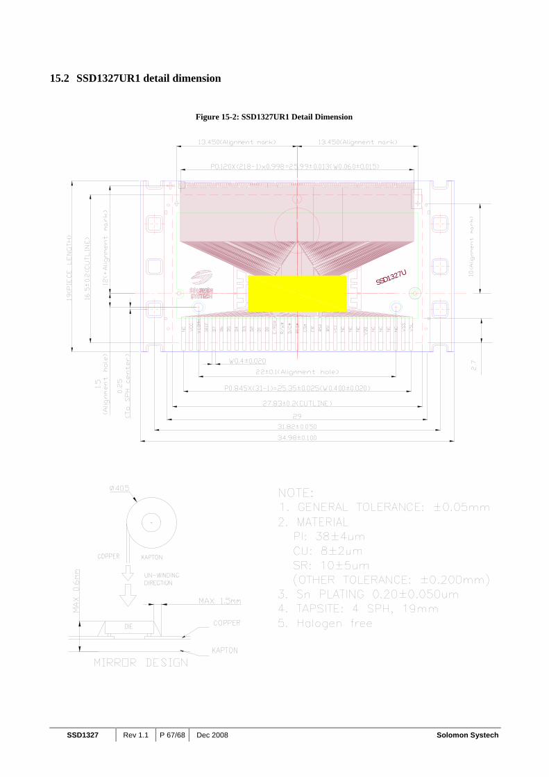
SSD1327 Rev 1.1 P 67/68 Dec 2008 Solomon Systech
15.2 SSD1327UR1 detail dimension
Figure 15-2: SSD1327UR1 Detail Dimension
SSD1327U
Solomon Systech Dec 2008 P 68/68 Rev 1.1 SSD1327
Solomon Systech reserves the right to make changes without notice to any products herein. Solomon Systech makes no warranty, representation or guarantee regarding the suitability of its products for any particular purpose, nor does Solomon Systech assume any liability arising out of the application or use of any product or circuit, and specifically disclaims any, and all, liability, including without limitation consequential or incidental damages. “Typical” parameters can and do vary in different applications. All operating parameters, including “Typical” must be validated for each customer application by the customer’s technical experts. Solomon Systech does not con-vey any license under its patent rights nor the rights of others. Solomon Systech products are not designed, intended, or authorized for use as components in systems intended for surgical implant into the body, or other applications intended to support or sustain life, or for any other application in which the failure of the Solomon Systech product could create a situation where personal injury or death may occur. Should Buyer purchase or use Solomon Systech products for any such unintended or unauthorized application, Buyer shall indemnify and hold Solomon Systech and its offices, employees, subsidiaries, affiliates, and distributors harmless against all claims, costs, damages, and expenses, and reasonable attorney fees arising out of, directly or indirectly, any claim of personal injury or death associated with such unintended or unauthorized use, even if such claim alleges that Solomon Systech was negligent regarding the design or manufacture of the part.
All Solomon Systech Products complied with six (6) hazardous substances limitation requirement per European Union (EU) “Restriction of
Hazardous Substance (RoHS) Directive (2002/95/EC)” and China standard “电子信息产品污染控制标识要求 (SJ/T11364-2006)” with
control Marking Symbol . Hazardous Substances test report is available upon requested.
http://www.solomon-systech.com