SPIRE Design Description -...
151
SPIRE Design Description SUBJECT: SPIRE Design Description PREPARED BY: Douglas Griffin Matt Griffin Bruce Swinyard DOCUMENT No: SPIRE-RAL-PRJ-000620 ISSUE: 1.0 Date: Monday 4 February 2002. 2.0 Thursday 15 May 2003 APPROVED BY: Date: Distribution: All SPIRE Co-Investigators and Institute Managers Change Record 1.0 4 February 2002 Update for IBDR All sections revised and updated based on subsystem DDRs and 2.0 15 May 2003 Updated information for the IHDR
Transcript of SPIRE Design Description -...

SPIRE Design Description
SUBJECT: SPIRE Design Description PREPARED BY: Douglas Griffin
Matt Griffin Bruce Swinyard
DOCUMENT No: SPIRE-RAL-PRJ-000620 ISSUE: 1.0 Date: Monday 4 February 2002. 2.0 Thursday 15 May 2003 APPROVED BY: Date: Distribution: All SPIRE Co-Investigators and Institute Managers Change Record 1.0 4 February 2002 Update for IBDR
All sections revised and updated based on subsystem DDRs and
2.0 15 May 2003 Updated information for the IHDR

SPIRE Design Description Document - 2.0
2
1. INTRODUCTION .....................................................................................................................................6
1.1 The SPIRE instrument and its scientific programme ........................................................................6 1.2 Purpose of this document ..................................................................................................................7 1.3 Scope.................................................................................................................................................8
2. INSTRUMENT OVERVIEW ...................................................................................................................9 2.1 Photometer design drivers.................................................................................................................9 2.2 Spectrometer design drivers............................................................................................................10 2.3 Instrument functional block diagram ..............................................................................................10
2.3.1 Imaging photometer....................................................................................................................12 2.3.2 Fourier transform spectrometer ..................................................................................................17 2.3.3 Helium-3 cooler ..........................................................................................................................20
3. Instrument System Design .......................................................................................................................24 3.1 SPIRE subsystems...........................................................................................................................24 3.2 The SPIRE instrument as a system .................................................................................................32 3.3 Structural design and FPU integration ............................................................................................36 3.4 Optical Design.................................................................................................................................38
3.4.1 Common optics and photometer optics ......................................................................................38 3.4.2 Spectrometer optical design........................................................................................................41
3.5 Straylight control.............................................................................................................................45 3.5.1 Bandpass filtering .......................................................................................................................45 3.5.2 Baffling .......................................................................................................................................46 3.5.3 Diffraction limited optical analysis.............................................................................................50 3.5.4 Optical alignment........................................................................................................................53
3.6 Thermal design................................................................................................................................53 3.6.1 Instrument temperature levels.....................................................................................................53 3.6.2 Cryogenic heat loads...................................................................................................................54 3.6.3 Temperature stability ..................................................................................................................55
3.7 EMC................................................................................................................................................55 3.7.1 Signal quality ..............................................................................................................................55 3.7.2 Grounding and RF shield............................................................................................................55 3.7.3 Microphonics ..............................................................................................................................61
3.8 System-level criticality ...................................................................................................................61 3.9 Redundancy scheme........................................................................................................................62 3.10 System budgets ...............................................................................................................................63
4. Subsystem Design....................................................................................................................................64 4.1 Warm Electronics............................................................................................................................64
4.1.1 Digital Processing Unit (HSDPU) ..............................................................................................65 4.1.2 Detector Readout and Control Unit (HSDRCU) ........................................................................72
4.2 RF Filters.........................................................................................................................................79 4.2.1 Subsystem Filters........................................................................................................................80 4.2.2 Detector and Bias Filters ............................................................................................................80
4.3 Bolometric Detector Arrays ............................................................................................................81 4.3.1 Principle of semiconductor bolometers ......................................................................................81 4.3.2 SPIRE bolometer performance requirements .............................................................................81 4.3.3 SPIRE bolometer design and specifications ...............................................................................82 4.3.4 Bolometer readout electronics ....................................................................................................83 4.3.5 Feedhorns and bolometer cavities...............................................................................................83 4.3.6 Bolometer array thermal-mechanical design ..............................................................................85
4.4 JFET units .......................................................................................................................................86 4.5 Mirrors ............................................................................................................................................90 4.6 Filters and beam splitters ................................................................................................................93
4.6.1 Photometer filtering scheme .......................................................................................................94 4.6.2 Spectrometer filtering scheme ....................................................................................................96
4.7 Internal calibrators ..........................................................................................................................98

SPIRE Design Description Document - 2.0
3
4.7.1 Photometer calibrator (PCAL)....................................................................................................98 4.7.2 Spectrometer calibrator (SCAL)...............................................................................................100
4.8 Beam Steering Mechanism (BSM) ...............................................................................................102 4.9 Spectrometer Mechanism..............................................................................................................108
4.9.1 Requirements on the mirror mechanism...................................................................................109 4.9.2 Control System and Readout ....................................................................................................111 4.9.3 The cryogenic mechanism (SMECm).......................................................................................112 4.9.4 Position measurement ...............................................................................................................112 4.9.5 The preamplifier (SMECp).......................................................................................................112
4.10 FPU structure ................................................................................................................................113 4.10.1 Mechanical Requirements ....................................................................................................115 4.10.2 Thermal Isolation Requirements ..........................................................................................115 4.10.3 Stray light and RF shielding.................................................................................................117 4.10.4 Alignment requirements .......................................................................................................118 4.10.5 Thermometry ........................................................................................................................119
4.11 Helium-3 Cooler ...........................................................................................................................120 4.11.1 Introduction ..........................................................................................................................120 4.11.2 Cooler components...............................................................................................................121 4.11.3 Cooler construction and thermo-mechanical design ............................................................122 4.11.4 Heat switch operation...........................................................................................................123 4.11.5 Cooler operation ...................................................................................................................123 4.11.6 Cooler redundancy ...............................................................................................................125
4.12 Thermal straps...............................................................................................................................126 4.12.1 Level-0 .................................................................................................................................126 4.12.2 300-mK Thermal Straps .......................................................................................................128
4.13 Harnesses and Connectors.............................................................................................................131 4.13.1 Passive thermal load.............................................................................................................132 4.13.2 Ohmic dissipation.................................................................................................................132 4.13.3 EMC, ESD and Signal Integrity Considerations ..................................................................132 4.13.4 Noise Budget Allocation ......................................................................................................134 4.13.5 Harness Reliability ...............................................................................................................134 4.13.6 Detector harnesses................................................................................................................135 4.13.7 Connectors............................................................................................................................135
5. Instrument Operating Modes .................................................................................................................139 5.1 Spacecraft pointing .......................................................................................................................139 5.2 Spacecraft movements during SPIRE observing ..........................................................................139
5.2.1 Nod ...........................................................................................................................................139 5.2.2 Raster ........................................................................................................................................141 5.2.3 Line Scan ..................................................................................................................................141
5.3 Photometer Observatory Functions...............................................................................................142 5.3.1 Point Source Photometry (POF1 and POF2) ............................................................................142 5.3.2 Jiggle Mapping (POF3 and POF4) ...........................................................................................144 5.3.3 Scan mapping (POF 4 and POF5).............................................................................................145 5.3.4 Photometer peak-up (POF7) .....................................................................................................145 5.3.5 Operation of photometer internal calibrator (POF8) ................................................................145
5.4 Spectrometer Observatory Functions............................................................................................146 5.4.1 Point source spectrum: continuous scan (SOF1) ......................................................................146 5.4.2 Fully-sampled spectral map: continuous scan (SOF2) .............................................................147 5.4.3 Point source spectrum: step-and-integrate (SOF3) ...................................................................147 5.4.4 Fully-sampled spectral map: step-and-integrate (SOF2) ..........................................................147
6. Spire Sensitivity Estimation...................................................................................................................148 7. References..............................................................................................................................................150

SPIRE Design Description Document - 2.0
4
Glossary
Term Meaning AIV Assembly, Integration and Verification AME Absolute Measurement Error AOCS Attitude and Orbit Control System APART Arizona's Program for the Analysis of Radiation Transfer APE Absolute Pointing Error ASAP Advanced Systems Analysis Program AVM Avionics Model BDA Bolometer Detector Array BFL Back Focal Length BOL Beginning of Life BRO Breault Research Organization BSM Beam Steering Mirror CDMS Command and Data Management System CDMU Command and Data Management Unit CDR Critical Design Review CMOS Complimentary Metal Oxide Silicon CPU Central Processing Unit CVV Cryostat Vacuum Vessel DAC Digital to Analogue Converter DAQ Data Acquisition DCU Detector Control Unit = HSDCU DPU Digital Processing Unit = HSDPU DQE Detective Quantum Efficiency DSP Digital Signal Processor EDAC Error Detection and Correction EGSE Electrical Ground Support Equipment EMC Electro-magnetic Compatibility EMI Electro-magnetic Interference EOL End of Life FCU FCU Control Unit = HSFCU FIR Far Infrared FIRST Far Infra-Red and Submillimetre Telescope FOV Field of View F-P Fabry-Perot FPGA Field Programmable Gate Array FPU Focal Plane Unit FSDL Fast Science Data Link. Used to transfer scientific data from the DRCU to the DPU FTS Fourier Transform Spectrometer FWHM Full Width Half maximum GSFC Goddard Space Flight Center HK House Keeping HOB Herschel Optical Bench HPDU Herschel Power Distribution Unit HSDCU Herschel-SPIRE Detector Control Unit HSDPU Herschel-SPIRE Digital Processing Unit HSFCU Herschel-SPIRE FPU Control Unit HSO Herschel Space Observatory IF Interface IID-A Instrument Interface Document - Part A IID-B Instrument Interface Document - Part B

SPIRE Design Description Document - 2.0
5
Term Meaning IMF Initial Mass Function IR Infrared IRD Instrument Requirements Document IRTS Infrared Telescope in Space ISO Infrared Space Observatory JFET Junction Field Effect Transistor JFP Photometer JFET Unit JFS Spectrometer JFET Unit LCL Latching Current Limiter LIA Lock-In Amplifier LSL Low Speed Link. Used for TC link between the DRCU and the DPU LVDT Linear Variable Differential Transformer LWS Long Wave Spectrometer (an instrument used on ISO) MAC Multi Axis Controller MCU Mechanism Control Unit = HSMCU M-P Martin-Puplett NEP Noise Equivalent Power NTD Neutron Transmutation Doped OBS On-Board Software OMD Observing Modes Document OPD Optical Path Difference PACS Photodetector Array Camera and Spectrometer PCAL Photometer Calibration source PID Proportional, Integral and Differential PLW Photometer, Long Wavelength PMW Photometer, Medium Wavelength POF Photometer Observatory Function PROM Programmable Read Only Memory PSW Photometer, Short Wavelength PUS Packet Utilisation Standard RMS Root Mean Squared SCAL Spectrometer Calibration Source SED Spectral Energy Distribution SMEC Spectrometer Mechanics SMPS Switch Mode Power Supply SOB SPIRE Optical Bench SOF Spectrometer Observatory Function SPIRE Spectral and Photometric Imaging Receiver SRAM Static Random Access Memory SSSD SubSystem Specification Document STP Standard Temperature and Pressure SVM Service Module TBC To Be Confirmed TBD To Be Determined TC Telecommand URD User Requirements Document UV Ultra Violet WE Warm Electronics ZPD Zero Path Difference

SPIRE Design Description Document - 2.0
6
1. INTRODUCTION
1.1 The SPIRE instrument and its scientific programme SPIRE (the Spectral and Photometric Imaging REceiver) is one of three cryogenic focal plane instruments for ESA’s Herschel mission. Its main scientific goals are the investigation of the statistics and physics of galaxy and structure formation at high redshift and the study of the earliest stages of star formation, when the protostar is still coupled to the interstellar medium. These studies require the capabilities to carry out large-area (many tens of square degrees) deep photometric imaging surveys at far-infrared and submillimetre wavelengths, and to follow up these systematic survey observations with spectroscopy of selected sources. SPIRE will exploit the advantages of Herschel: its’ large-aperture, cold, low-emissivity telescope; the complete lack of atmospheric emission and attenuation giving access to the poorly explored 200-700-µm range, and the large amount of high quality observing time. Because of these advantages, SPIRE will have unmatched sensitivity for deep imaging photometry and moderate-resolution spectroscopy. Galaxies emit a large amount (from 30% to nearly 100%) of their energy in the far infrared due to re-processing of stellar UV radiation by interstellar dust grains. The far infrared peak is redshifted into the SPIRE wavelength range for galaxies with redshift, z, greater than ~ 1. The total luminosity of a galaxy cannot be determined without an accurate measurement of its Spectral Energy Distribution (SED). The study of the early stages of galaxy evolution thus requires an instrument that can detect emission from high-z galaxies in the submillimetre, enabling their SEDs and luminosities to be derived. Stars form through the fragmentation and collapse of dense cloud cores in the interstellar medium (ISM), and the very first stages of this process are not well known. A good understanding of this early evolution is crucial, as it governs the origin of the stellar initial mass function (IMF). Sensitive far infrared and submillimetre observations with high spatial resolution are necessary to make complete surveys of protostellar clumps to determine their bolometric luminosities and mass functions. SPIRE will also, for the first time, enable astronomers to observe at high spatial resolution the physical and chemical conditions prevailing in the cold phases of the interstellar medium and to study the behaviour of the interstellar gas and dust before and during star formation. SPIRE’s uniquely high sensitivity to very cold dust emission also makes it the ideal instrument to study the material that is ejected in copious quantities from evolved stars, enriching the interstellar medium with heavy elements. Large amounts of matter - as yet undetected - are ejected from stars before the white dwarf stage. Theories of stellar evolution, and of the enrichment of galaxies in heavy elements and dust, will be incomplete until these earlier mass loss phases are characterised and understood. Studies of star formation and of the interaction of forming and evolved stars with the ISM are also, of course, intimately related to the investigation of galaxy formation and evolution, which occur through just these processes. These high priority programmes for Herschel require sensitive continuum imaging in several bands to carry out surveys, and a low-resolution spectroscopic mode to obtain detailed SEDs of selected objects and measure key spectral lines. Although SPIRE has been optimised for these two main scientific programmes, it will offer the astronomical community a powerful tool for many other astrophysical studies: giant planets, comets, the galactic interstellar medium, nearby galaxies, ultraluminous infrared galaxies, and active galactic nuclei. Its capabilities will remain unchallenged by the ground-based and the airborne observatories which are planned to come into operation over the next decade. The scientific case for SPIRE is described in more detail in the SPIRE proposal (Griffin et al., 1998a)

SPIRE Design Description Document - 2.0
7
1.2 Purpose of this document This document outlines the essential features of the design and operation of SPIRE. It is intended to provide an introductory account of the key features of the SPIRE system and subsystem design and operation - but not to provide a complete description: for that the reader is referred to other more detailed project documents, particularly the following: Document Reference Abbreviation SPIRE Scientific Requirements
SPIRE-UCF-PRJ-000064 SRD
SPIRE Instrument Interface Document Part B
SPIRE-ESA-DOC-000275 IID-B
SPIRE Instrument Requirements Specification
SPIRE-RAL-PRJ-000034/1.0 23 Nov. 2000 IRD
Operating Modes for SPIRE
SPIRE-RAL-PRJ-000320 OMD
SPIRE On-Board Software URD
SPIRE-IFSI-PRJ-000444/ OBS URD
Detector Subsystem Specifications
Doc.: SPIRE-JPL-PRJ-456 Date/Issue: 17 April 2001, Ver: 1.9
SPIRE Spectrometer Mirror Mechanism Subsystem Specification
Doc.: LAM.PJT.SPI.SPT.200002 Date/Issue: 12 October 2001, Issue 8
SPIRE Beam Steering Mirror Subsystem Specification Document
Doc.: SPIRE-ATC-PRJ-0460 Date/Issue: 10 July 2001, v. 3.2
SPIRE Sorption Cooler Specifications
Doc.: GS/SBT/SPIRE/2000-01 Date/Issue: 05/2001, 1. Rev.2
DPU Subsystem Specification Document
Doc.: SPIRE-IFS-PRJ-000462 Date/Issue: 26/11/01, Issue 1.2
MCU Design Description Doc.: LAM/ELE/SPI/000619/1.1/ 20 Date/Issue: Dec. 2000
SPIRE Mirrors Specification Doc.: LAM.PJT.SPI.SPT.200007 Ind 7 Date/Issue: 12 July 2001, Issue 7
DRCU Subsystem Specification
Doc.: SAp-SPIRE-CCa-25-00 Date/Issue: 29/7/01, 0.9
SPIRE Filters subsystem specification
Doc.: SPIRE-PRJ-000454 Date/Issue:
SPIRE Spectrometer Calibrator subsystem specification
Doc.: HSO-CDF-DD-33 Date/Issue: 1.0 5 September 2001
SPIRE Photometer Calibrator subsystem specification
Doc.: HSO-CDF-SP-003 Date/Issue: 1.0, 5 September 2001
Subsystem Specification Documents for each of the SPIRE subsystems
SPIRE Structure Subsystem Specification Document
Doc.: MSSL/SPIRE/SP003.13 Date/Issue: 29 Nov 2001
SSSDs
Additional references are given in Section 7.

SPIRE Design Description Document - 2.0
8
1.3 Scope The document concerns the design and operation of the instrument. It includes:
(i) the Warm Electronics (WE) which is composed of the Digital Processor Unit (DPU), the Detector Control Unit (DCU) and the FPU Control Unit (FCU) and their associated electrical harnesses;
(ii) the Focal Plane Unit (FPU) which contains the optical components, detector arrays, 300-mK sorption cooler, mechanisms, internal calibrators, thermal straps, and various housekeeping units, and the mechanical structure which houses these elements;
(iii) The Photometer JFET unit (JFP) and the Spectrometer JFET Unit (JFS) which are both located on the Herschel Optical Bench.
(iv) the on-board software (OBS) which allows commanding of the instrument and telemetry of the science and housekeeping data.
The design of the Herschel telescope, which SPIRE shares with the other experiments, is only referenced to in as much as it influences the design of SPIRE. The thermal straps from the Herschel cryostat to the FPU, the interface between the DPU and the spacecraft Power Distribution Unit and the Command and Data Handling System (CDMS) are only referenced only in so far as they impact on the design of the units listed above. The various items of SPIRE ground support equipment also fall outside the scope of the document. The purpose of this document is to provide the reader with an overview of the SPIRE design and an understanding of the rationale for the design choices. Although the document will be updated periodically to reflect the evolution and detailing of the instrument design, the information contained herein is not necessarily accurate in all details, and this document should therefore not be used as a reliable source of design information. To obtain the most up-to-date information, the reader is directed to the appropriate project documents (IID-B, IRD, SSSDs and other system and subsystem documents)

SPIRE Design Description Document - 2.0
9
2. INSTRUMENT OVERVIEW SPIRE contains a three-band imaging photometer and an imaging Fourier Transform Spectrometer (FTS), both of which use 0.3-K feedhorn-coupled “spider-web” NTD germanium bolometers cooled by a 3He refrigerator. The photometer and spectrometer are not designed to operate simultaneously. The field of view of the photometer is 4 x 8 arcminutes, the largest that can be achieved given the location of the SPIRE field of view in the Herschel focal plane and the size of the telescope unvignetted field of view. Three bolometer arrays provide broad-band photometry (λ/∆λ ~ 3) in wavelength bands centred at approximately 250, 360 and 520 µm. (For historical reasons, these are sometimes referred to as the 250-, 350- and 500-µm bands. The field of view is observed simultaneously in all three bands through the use of fixed dichroic beam-splitters. Spatial modulation can be provided either by a Beam Steering Mirror (BSM) in the instrument or by scanning the telescope across the sky, depending on the type of observation. An internal thermal calibration source is available to provide a repeatable calibration signal for the detectors. The FTS uses novel broadband intensity beam splitter, and combines high efficiency with spatially separated input ports. One input port covers a 2.6-arcminute diameter field of view on the sky and the other is fed by an on-board calibration source. Two bolometer arrays are located at the output ports, covering two overlapping spectal bands, 200-325 µm and 315-670 µm. The spectral resolution, as determined by the maximum optical path difference, will be adjustable between 0.04 and 2 cm-1 (corresponding to λ/∆λ = 1000 - 20 at 250 µm wavelength. The FTS can be operated in continuous scan mode, with the path difference between the two arms of the interferometer being varied by a constant-speed mirror drive mechanism or in step-and-integrate mode in which the scan-mirror is sequentially positioned at a range of positions with the interferogram built up from individual measurements at each step. In this mode, signal modulation will be provided by the BSM.
2.1 Photometer design drivers The basic design of the photometer was dictated by the following consideration:
(i) the major scientific priorities for SPIRE require an instrument which is capable of deep mapping of large areas of sky efficiently with full spatial sampling and multi-wavelength coverage;
(ii) observations of point and compact sources should also be possible with good efficiency;
(iii) the instrument should be as simple as possible for affordability, reliability and ease of operation;
(iv) the wavelength coverage should complement that of the PACS instrument on board Herschel and ground-based facilities operating at near-millimetre wavelengths;
These considerations led to the choice of a system with fixed dichroic beamsplitters allowing simultaneous observation of a large field of view in the three chosen submillimetre bands, with the inclusion of a beam steering mirror to allow point source observations and small maps to be carried out efficiently.

SPIRE Design Description Document - 2.0
10
2.2 Spectrometer design drivers Fabry-Perot and grating spectrometer designs were also studied for SPIRE (Griffin, 1997; Griffin et al. 1998b). The FTS was chosen for a number of reasons:
(i) it allows for two-dimensional imaging spectroscopy, which is not possible with the grating instrument;
(ii) the spectral resolution can easily be adjusted and tailored to the scientific requirements of the observation;
(iii) the detectors can be operated at 300 mK because the photon noise limited NEP is higher for the FTS, whose detectors observe broad-band, than for grating or Fabry-Perot spectrometers in which they observe in narrow-band mode - this allowed a 3He sorption cooler to be adopted for SPIRE - a considerable simplification over the 100-mK dilution cooler that would have been needed for a grating or F-P instrument;
(iv) whilst the grating is more sensitive, at least in principle, for observations of known spectral lines, there is little difference in the sensitivities of the two options for spectral survey observations, which are of greater scientific priority for SPIRE;
(v) the FTS is less vulnerable to degradation in performance arising from stray light and out-of-band leaks which can be problematic with a low-background grating instrument;
(vi) practical implementation of either a grating or an F-P instrument within the constraints of the Herschel system would have posed serious accommodation problems (grating) or risk of FPU failure due to having multiple mechanisms in series (F-P).
2.3 Instrument functional block diagram Figure 2-1 shows a functional block diagram of the SPIRE instrument. The subsystems are prefixed HS standing for Herschel-SPIRE. The focal plane unit is mounted on the Herschel Optical Bench as shown in Figure 2-2. It is approximately 690 x 410 x 410 mm in size, and has three separate temperature stages at nominal temperatures of 4 K (Herschel cryostat Level-1), 2 K (cryostat Level-0) and 300 mK (provided by SPIRE's internal cooler). The main Level-1 structural element of the FPU is an optical bench panel which is isostatically mounted on the cryostat optical bench (Level-2, approx. 10 K) by two stainless steel blade mounts and a single stainless steel cone mount. The photometer and spectrometer are located on either side of this panel. The majority of the optics are at Level-1, but the detector arrays and final optics are contained within Level-0 enclosures. The 3He refrigerator cools all of the five detector arrays to 0.3 K. Two JFET preamplifier boxes (one for the photometer and one for the spectrometer) are attached to the Level-2 optical bench close to the Level-1 enclosure. The two JFET units are heated internally to their optimum operating temperature of ~ 120 K. The SPIRE warm electronics consist of a Detector Readout Unit (DCU), a FPU Control Unit (FCU) and a Digital Processing Unit (DPU). The DCU provides bias and signal conditioning for the arrays and cold readout electronics and reads out the detector signals; the FCU controls the FPU mechanisms, the 3He cooler and the internal calibrators, and housekeeping thermometers. The DPU acts as the interface to the spacecraft, including instrument commanding, and formats science and housekeeping data for telemetry to the ground.

SPIRE Design Description Document - 2.0
11
FPU Structure
SMEC SMEC
Optics
Filters, Beam dividers,Dichroics
Baffles
Warm Interconnect Harness (HSWIH)
SPIRE HSFPU
Opt. BenchCVV Wall
Spacecraft Electronics
RF Filter RF Filter
FPU Control Unit (HSFCU)
Spacecraft PowerDistribution Unit
BSMPhot . Cal. Source
BSMPhot . Cal. Source
FTS Cal. Source Detector Arrays (0.3 K)
Spacecraft Command and Data Management System
(CDMS)
Digital Processing Unit (HSDPU)
JFET Boxes
Cooler Shutter Thermometers
P1P1
Detector Control Unit (HSDCU)
Mirrors
SPIRE Warm Electronics on SVM
JFP JFS
P2P2 P3P3 S3 S3 S3 S3
SPIRE EGSE
RF Filter RF Filter RF
Filter RF Filter RF
FilterRF
FilterRF
FilterRF
FilterRF
FilterRF
Filter
Figure 2-1 - Functional block diagram of the SPIRE instrument
Figure 2-2 - Location of the SPIRE FPU with respect to the other instruments on the Herschel Optical
Bench.

SPIRE Design Description Document - 2.0
12
Figure 2-3 – Perspective view of SPIRE and the other Herschel instruments on the Herschel Optical
Bench.
2.3.1 Imaging photometer
2.3.1.1 Optical Design and FPU layout The photometer layout is shown in Fig. 2.3. The Level-1 optical elements are mounted directly on the SPIRE Optical Bench (SOB). The Level-0 Photometer Detector Box is also supported on the SOB by stainless steel blades, and contains the Bolometer Detector Arrays (BDAs), dichroics, and fold mirrors. The three BDAs are bolted to the outside wall of the Level-0 box. Within each module, the detector arrays, feedhorns and the final filter are thermally isolated from the Level-0 structure by Kevlar wires, and are cooled by a thermal strap to the 3He refrigerator (see §4.11 below). The photometer input optics are shared with the spectrometer. The separate spectrometer field of view is directed to the other side of the optical bench panel by a pick-off mirror.

SPIRE Design Description Document - 2.0
13
Figure 2-4 - Solid model of the SPIRE photometer (4-K cover not shown)
The photometer optical design is shown in Figure 2-5, and is described in more detail by Dohlen et al. (2000) and in §2.3.1 below. It is an all-reflective system except for two dichroic beam splitters used to direct the three wavelength bands onto different bolometer arrays, and various transmissive band-pass and edge filters used to reject out-of-band radiation. It is optimised to give close to diffraction-limited imaging across the whole 4 x 8 arcminute field of view. The SPIRE field of view is offset by 11 arcminutes from the centre of the Herschel telescope's highly curved focal surface. Mirror M3, which lies below the focus, receives the f/8.68 beam from the telescope and forms a pupil image of the telescope secondary at the flat beam steering mirror, M4. Mirror M5 converts the focal ratio to f/5 and provides an intermediate focus at the next mirror, M6, which re-images the aperture stop at M4 to a cold stop located at the entrance to a Level-0 enclosure. M7, M8 and M9 constitute a one-to-one optical relay to bring the M6 focus to the three detector arrays. The beams for the three bands are directed onto the arrays at f/5 by a combination of flat folding mirrors and fixed dichroics set at 25º to the beam axis. M3 - M8 are at Level-1 and the cold stop and all subsequent optics are at Level-0.

SPIRE Design Description Document - 2.0
14
CM4
CM3CM5
PM6
PM7
PM8
PM9
Figure 2-5 - Imaging photometer optical design
Initially, it was envisaged that a shutter at the entrance aperture of the instrument (just above the telescope focus) would be used to block the beam during ground testing. This piece of hardware has been removed and provision has been made in the satellite ground test cryostat (and to an extent in the flight cryostat) for the provision of a low background in the three Herschel instruments’ field-of-views. An internal calibration source provides a repeatable signal for the bolometer arrays. It radiates through a 2.8-mm hole in the centre of the beam steering mirror, M4. As this is at a pupil image, the illumination is close to uniform over the arrays. The source will be modulated at frequencies of a few Hz, and will provide a high instantaneous S/N with peak power dissipation < 2 mW. The beam steering mirror is capable of chopping ±2 arcminutes along the long axis of the 4 x 8 arcminute field of view, at frequencies up to 2 Hz with an efficiency of 90% and power dissipation < 4 mW. It can operate at higher frequencies with reduced efficiency and increased power dissipation. The beam steering mechanism can simultaneously chop at up to 1 Hz in the orthogonal direction by up to 30 arcseconds. Two axis motion allows "jiggling" of the pointing to create a fully sampled image of the sky with the feedhorn-coupled detectors whose diffraction-limited beams on the sky are separated by approximately twice the beam FWHM. The SPIRE filtering scheme is designed to provide precise definition of the spectral passbands with high out-of-band rejection and maximum in-band transmission, and also to minimise the thermal loading on the 4-K, 2-K and 0.3-K stages by reflecting short-wavelength radiation. To achieve complete rejection out to UV wavelengths, four blocking filters are needed in the chain in addition to high-pass and low-pass edge filters which define the band.

SPIRE Design Description Document - 2.0
15
2.3.1.2 Photometer Bolometer Detector Arrays SPIRE will use spider-web bolometers with NTD germanium thermometers (Bock et al. 1998, Turner et al. 2002). The bolometers are coupled to the telescope by hexagonally close-packed single-mode conical feedhorns, providing diffraction limited beams. The horn diameters are 2Fλ where F is the focal ratio of the final optics and λ is the wavelength: this provides a diffraction-limited beam with maximum coupling efficiency of the detector to a point source. The feedhorn centre-centre spacings are defined at wavelengths of 250, 333, and 500 µm. The value of 333 µm is selected to provided exact overlap between a significantly larvge sets of detectors in all three of the arrays. The numbers of detectors in the three arrays are 139, 88, and 43 for 250, 350 and 500 µm respectively, making a total of 270 detectors for the photometer. The detector arrays are shown schematically in Figure 2-6a and Figure 2-6b is a photograph of a prototype array module. Modelling of the complete optical train predicts FWHM beam widths of 17.1, 24.4 and 34.6 arcseconds at 250, 350 and 500 µm, respectively Each array unit has an interface to the Level-0 box, with a thermal strap from the 3He cooler to the 0.3-K stage, which is supported by Kevlar strings from Level-0. The electrical connections to the detectors are made with Kapton ribbon cables within the array modules and with woven manganin cables between the array modules and the JFET units. The bolometers are excited by an AC bias at a frequency of approximately 100 Hz, which eliminates 1/f noise from the JFETs, giving a 1/f knee for the system of less than 100 mHz..
2.3.1.3 Photometer observing modes The photometer will have three principal observing modes, as illustrated in Figure 2-7 and described below. These modes are described in greater detail in OMD.
Figure 2-6 - (a) layout of the three photometer arrays; (b) photograph of array mechanical prototype.
Point source photometry: For photometric observations of point or compact sources, chopping will be used. There are several sets of three detectors for which the beams at the three wavelengths are exactly co-aligned on the sky, indicated by the shaded circles in Figure 2-6. By

SPIRE Design Description Document - 2.0
16
chopping through the appropriate angle (approx. 126 arcseconds), 3-band photometric observations can be carried out simultaneously with maximum efficiency. To account for the possibility of positional errors due to telescope pointing inaccuracy or imperfect knowledge of the source position, the beam steering mirror can be used to implement a seven-point mapping routine in this mode. Assuming an angular offset of 6" for the seven-point, the loss in S/N for a given integration time varies between 6% at 500 µm and 20% at 250 µm, which is a small penalty to pay for assurance that telescope pointing or source position errors do not result in an underestimate of the source flux density. Field mapping: For mapping of regions a few arcminutes in extent, the beam steering mirror will be used to carry out a jiggle map, similar to the mode of operation of the SCUBA bolometer camera on the JCMT (Holland et al. 1999). A 64-point jiggle pattern is needed to achieve full spatial sampling in all bands simultaneously, with a step size of 9 arcseconds (half-beam spacing at 250 µm). A maximum field size of 4 x 4 arcminutes is available in this mode as the 2-arcminute regions at each end of the array will be chopped outside the field of view admitted by the photometer optics. Scan mapping: This mode will be used for mapping large areas of sky (much bigger than the SPIRE field of view), including deep survey observations. The telescope will be scanned across the sky (at up to 1 arcminute per second, the maximum rate that the spacecraft can provide). Because of the excellent 1/f stability of the NTD detectors, the beam steering mirror does not need to be operated - signal modulation is provided by the telescope motion. To provide the necessary beam overlap for full spatial sampling over the strip defined by a single scan, the scan angle must be 14.5o with respect to one of the array axes. The available Herschel telemetry rate (at least 100 kbs, perhaps up to 140 kbs) allows all of the 270 photometer detectors to be sampled with 16-bit resolution at up to 28 Hz. This data is stored in Hershel bulk memory and telemetered directly during ground contact periods with no on-board processing.

SPIRE Design Description Document - 2.0
17
Figure 2-7 - Overlaid photometer arrays and summary of photometer observing modes.
2.3.2 Fourier transform spectrometer
2.3.2.1 Optical design and FPU layout The layout of the FTS and its optical scheme are shown in Figure 2-8 and Figure 2-9 respectively. The main design features of the FTS are described in Swinyard et al. (2000) and in §3.4.2 below. It uses two broadband, high-efficiency, intensity beam splitters in a Mach-Zehnder configuration rather than the traditional polarising beam splitters. This configuration has the advantage that all four ports are separately accessible, as in the classical Martin Puplett (M-P) polarising FTS (Martin, 1982). But the throughput is a factor of two higher than for the M-P as none of the incoming radiation is rejected. This design is also insensitive to the polarisation of the incident radiation. The performance of the beam splitters and of a bench-top implementation of this design has been demonstrated (Ade et al. 1999). A thermal calibrator (P-Cal) is located at a pupil image in the second input port of the FTS, and provides a thermal input that mimics the dilute 80-K black body emission of the telescope. This allows the large telescope background to be nulled, thereby reducing the dynamic range requirements for the detector sampling. Two band-limited detector arrays are placed in the two output ports, covering 200-325 µm and 315-670 µm. These bands are referred to as the S/SW and S/LW bands, respectively. A single back-to-back moving rooftop mechanism serves both arms of the interferometer, with a frictionless carriage mechanism using double parallelogram linkage and flex pivots. The pick-off mirror (on the photometer side of the optical bench panel and located at the intermediate field image) directs the spectrometer field of view through a hole in the optical bench panel into the FTS side of the instrument. A 4-K pupil stop is located between the pick-off mirror and the input fold mirror. The input relay mirror focuses the beam to an intermediate image plane located just after the first beam splitter, after which the beam is collimated and sent to the moving rooftop mirror assembly. The rooftop mirror

SPIRE Design Description Document - 2.0
18
shifts the beam and sends it towards the camera mirror, which produces an image plane just before the output beam splitter. The output relay mirror focuses the beam onto the detector arrays. A pupil image is located near the final fold mirror, making this a convenient location for the entrance aperture to the Spectrometer Detector Box. As this pupil moves when the optical path difference changes, it is not a good place for a limiting cold stop. Instead, the limiting aperture is located at the 4-K pupil plane between the pick-off mirror and the input fold mirror.
Figure 2-8 - Physical layout of the spectrometer.
SPIRE Design Description Document - 2.0
19
M3M5
M6sCollCam M7sRinRout
FoldBS1BS2
Det
CC
M4
CM3
CM4
CM5
SM7
SM6
SBS1SCCA
SM9ASM10A
SBS2
SM11A
SM12A
SSW
SM8A
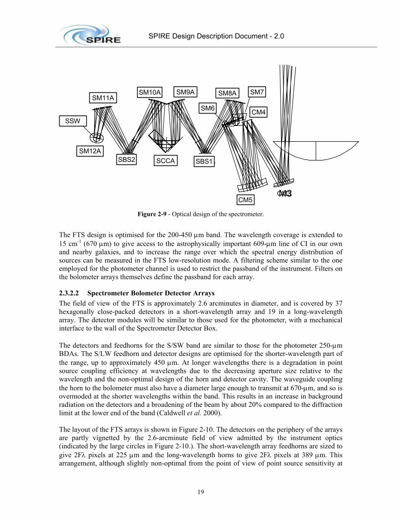
Figure 2-9 - Optical design of the spectrometer.
The FTS design is optimised for the 200-450 µm band. The wavelength coverage is extended to 15 cm-1 (670 µm) to give access to the astrophysically important 609-µm line of CI in our own and nearby galaxies, and to increase the range over which the spectral energy distribution of sources can be measured in the FTS low-resolution mode. A filtering scheme similar to the one employed for the photometer channel is used to restrict the passband of the instrument. Filters on the bolometer arrays themselves define the passband for each array.
2.3.2.2 Spectrometer Bolometer Detector Arrays The field of view of the FTS is approximately 2.6 arcminutes in diameter, and is covered by 37 hexagonally close-packed detectors in a short-wavelength array and 19 in a long-wavelength array. The detector modules will be similar to those used for the photometer, with a mechanical interface to the wall of the Spectrometer Detector Box. The detectors and feedhorns for the S/SW band are similar to those for the photometer 250-µm BDAs. The S/LW feedhorn and detector designs are optimised for the shorter-wavelength part of the range, up to approximately 450 µm. At longer wavelengths there is a degradation in point source coupling efficiency at wavelengths due to the decreasing aperture size relative to the wavelength and the non-optimal design of the horn and detector cavity. The waveguide coupling the horn to the bolometer must also have a diameter large enough to transmit at 670-µm, and so is overmoded at the shorter wavelengths within the band. This results in an increase in background radiation on the detectors and a broadening of the beam by about 20% compared to the diffraction limit at the lower end of the band (Caldwell et al. 2000). The layout of the FTS arrays is shown in Figure 2-10. The detectors on the periphery of the arrays are partly vignetted by the 2.6-arcminute field of view admitted by the instrument optics (indicated by the large circles in Figure 2-10.). The short-wavelength array feedhorns are sized to give 2Fλ pixels at 225 µm and the long-wavelength horns to give 2Fλ pixels at 389 µm. This arrangement, although slightly non-optimal from the point of view of point source sensitivity at

SPIRE Design Description Document - 2.0
20
the central wavelengths of the two arrays, has the advantage that there are numerous co-aligned pixels in the combined field of view. This maximises the observing efficiency for measuring a point source spectrum together with its surrounding sky background and also provides redundancy to the spectrometer in the case of failure of a single pixel within one array.
Figure 2-10 - Layout of spectrometer detector arrays
2.3.2.3 Spectrometer observing modes The FTS will be operated in continuous scan mode with the mirrors moving at a constant speed of up to 0.1 cm s-1, corresponding to a signal frequency range of 6 - 20 Hz. The spectral resolution can be adjusted between 0.04 and 2 cm-1 (λ/∆λ = 20 - 1000 at 250 µm). The maximum scan length is 3.5 cm (taking 35 seconds or more and giving an optical path difference of 14 cm). To ensure that mechanism jitter noise is well below the photon noise level, a relative accuracy of 0.1 µm is required for the mirror position. The FTS calibration source will be on continuously while the spectrometer is operating, with a peak power of no more than 5 mW. For spectral mapping of extended sources, the beam steering mirror will be used to provide the necessary pointing changes between scans. The scanning mirror control system uses a digital feedback loop to provide a constant speed over the scan length, with an accuracy requirement of 1% (goal 0.5%). The position readout uses a Heidenhain Moiré fringe sensing system. The detectors are read out asynchronously with the samples time-stamped to match them to the corresponding mirror locations. No on-board processing will be done - the raw interferograms will be telemetered to the ground. The number of detectors and the available telemetry rate are compatible with an oversampling factor of two with respect to the Nyquist sampling rate of 40 Hz (sampling at approx. 80 Hz per detector). An oversampling factor somewhat greater than this is desirable - options to achieve this include increasing the data rate, decreasing the mirror speed, sampling only a fraction of the detectors in some cases (e.g., point source observations), or a combination of these.
2.3.3 Helium-3 cooler The 3He cooler (Duband 1997) uses porous material to adsorb or release a gas when cooled or heated. This type of refrigerator is well-suited to a space environment. Gas-gap heat switches (Duband 1995) are used the control the refrigerator and there are no moving parts. It can be

SPIRE Design Description Document - 2.0
21
recycled indefinitely with over 95% duty cycle efficiency and the lifetime is only limited by that of the cold stage from which it is run (in this case, the lifetime of the Herschel cryostat). The evaporation of 3He naturally provides a very stable operating temperature under constant heat load over the entire cycle. The cooler requires no mechanical or vacuum connections and only low-current electrical leads for its operation, making the mechanical and electrical interfaces very simple. For operation in a zero-g environment two aspects of the design of a 3He refrigerator have been addressed: the liquid confinement and the structural strength required for the launch. The confinement within the evaporator is provided by a porous material which holds the liquid by capillary attraction. For the thermal isolation and structural support of the refrigerator elements, a suspension system using Kevlar wires has been designed to support the cooler firmly during launch whilst minimising the parasitic heat load on the system. The base-line SPIRE cooler contains 6 STP litres of 3He, fits in a 200 x 100 x 100 mm envelope and weighs about 1.6 kg. Its performance has been analysed using the same methods that successfully predicted the performance of the IRTS cooler on orbit. When operated from a 1.8-K heat sink it achieves a temperature of 287 mK at the evaporator with a 10 µW heat load, a hold time of at least 46 hours and a duty cycle efficiency of 96%. The energy input to the helium tank during recycling of the fridge is about 700 Joules. The 3He cooler is a potential single point failure for the instrument. Various options for redundancy have been considered. The chosen option is to implement a single cooler with non-redundant heats switches. The critical heaters and thermistors on the heat switches and on the pump are fully redundant and double-wired where appropriate. The reliability and redundancy have been analyzed (Collerias, 2001), and the results are satisfactory. Figure 2-11is a photograph of a development model cooler which is similar to the SPIRE design.

SPIRE Design Description Document - 2.0
22
Figure 2-11 - View of a prototype SPIRE cooler


3. INSTRUMENT SYSTEM DESIGN In this section the SPIRE instrument is described in terms of its systems level implementation. First an overview is given of the SPIRE instrument subsystem implementation, then the instrument is described as a number interacting systems. Finally a more detailed description is given of the systems design approach taken in the critical areas of structural design; optical design; thermal design; electrical design and EMI protection.
3.1 SPIRE subsystems The SPIRE instrument can be divided into two separate sections, the cryogenic subsystems located on the Herschel Optical Bench (HOB) inside the Cryostat Vacuum Vessel (CVV) and the Warm Electronics (WE) which are located outside the CVV on the Herschel Service Module SVM below the CVV. A schematic diagram of the SPIRE subsystems inside the CVV is shown in Figure 3-1. The following features are illustrated in this Figure.
• The Herschel Optical Bench (HOB) upon which SPIRE, PACS and HIFI are mounted is shown with black hatching.
• The thermal straps between the various stages of the cryostat, cryocooler and the detector boxes are shown as blue hatching
• The Photometer and Spectrometer Detector Boxes which are kept at 2 K are shown are indicated by blue crosses.
• The 4-K FPU is indicated by green crosshatching. This unit is sealed to prevent the ingress of EMI and/or stray light. .
• Internal stay light baffles are indicated by black hatching. • Indicative harness routing is shown by magenta. • The light rays from the telescope is shown by red lines.
The only interface between the SPIRE subsystems inside the CVV and the WE on the SVM is via the bulk-head connectors (and associated harnesses) shown at the top of Figure 3-1. The SPIRE harnesses that connect the outside of the CVV to the WE are shown on the left hand side of Figure 3-2. This schematic shows the Detector Readout and Control Unit (DRCU), which consists of two sub-units; the Focal-Plane Control Unit (FCU) and the Digital Control Unit (DCU), together with the electrical interfaces to the Herschel spacecraft. Figure 3-3 and Figure 3-4 show views of the photometer and the spectrometer with the physical locations of the various subsystems. Table 3-1 lists and describes the sub-systems and gives the unit names used in the IID-B. A detailed description of the design of all the SPIRE subsystems is given in §4.

SPIRE Design Description Document - 2.0
25
Figure 3-1 - Schematic diagram of the sub systems of SPIRE contained within the Herschel CVV.

SPIRE Design Description Document - 2.0
26
Figure 3-2 - Schematic diagram of the sub-systems of SPIRE contained on the Herschel SVM.
The only interface between the SPIRE subsystems inside the CVV and the WE on the SVM is via the 13 bulk head connectors (and associated harnesses) shown at the top of Figure 3-1. The SPIRE harnesses that connect to the outside of the CVV connect to the WE on the left hand side of Figure 3-2. This schematic shows the Detector Readout and Control Unit (DRCU), the Focal-Plane Control Unit (FCU), the Digital Control Unit (DCU) and the electrical interfaces with the Herschel spacecraft. Figure 3-3 and Figure 3-4 show views of the photometer and the spectrometer with the various subsystems. A detailed description of the design of all the systems of SPIRE is given in §4.

Figure 3-3 - View of photometer side of the instrument. The photometer cover is shown rotated to expose the photometer componts.

SPIRE Design Description Document - 2.0
28
Figure 3-4 - View of the spectrometer side of the FPU. The cover is shown rotated to expose the components house beneath the cover.

A complete list of the description of the design of all the sub systems of SPIRE is given in §4.

SPIRE Design Description Document - 2.0
30
Subsystem Name
Description Unit Redundancy
Structure
Focal plane unit structure to hold all cold sub-systems in the focal unit. This includes all thermometers necessary to monitor the instrument during cool down and operation.
HSFPU No redundancy
Optics All mirrors for the photometer and spectrometer channels
HSFPU No redundancy
Filters All filters; beam splitters and dichroics for the photometer and spectrometer channels The requirements on these are included with those for the optics.
HSFPU No redundancy
Baffles Straylight control baffles for the photometer and spectrometer channels
HSFPU No redundancy
Cooler 3He cooler unit cools the photometer and spectrometer detector arrays to 300 mK
HSFPU No redundancy on hardware, full redundancy on control system and harnessing
Bolometer Detector Arrays (BDAs)
Bolometer array modules for the photometer and spectrometer
HSFPU No redundancy. Loss of a single bolometer element is a soft failure mechanism but several hard failure mechanisms exist
Beam Steering Mechanism (BSM)
This mechanism allows the photometer and spectrometer fields of view to be stepped or chopped across the sky.
HSFPU No redundancy in the structure, mirror or flexure pivots. Redundancy in instrumentation, actuation and harnessing.
FTS Mechanism (SMECm)
The FTS moving mirrors drive mechanism and position measurement system. SMECm designates the mechanism and position encoder
HSFPU No redundancy in the structure, mirror or flexure pivots. Redundancy in instrumentation, actuation and harnessing.
FTS encoder amplifier (SMECp)
SMECp the cold pre-amplifier for the position encoder detectors.
HSFPU Fully redundant
Shutter Mechanism
A shutter is required in the instrument for ground test to allow the detectors to see the correct radiation environment.
HSFPU No redundancy as not a flight item.
Photometer Calibration Source
Calibration source for photometer HSFPU No redundancy on light guide and reference source. Full redundancy on electronics and harnesses.

SPIRE Design Description Document - 2.0
31
Subsystem Name
Description Unit Redundancy
Spectrometer Calibration Source (SCAL)
Calibration source for the spectrometer HSFPU Redundancy on reference source heater and thermometer. Full redundancy on electronics, heater and harnesses.
RF Filter Modules
Each sub-system harness into the cold FPU must have an electrical RF filter to prevent EMI problems with the bolometers. These will be mounted in standard RF filter modules on the wall of the FPU box.
HSFPU Fully redundant
Photometer JFET Box
JFET pre-amplifiers for photometer NTD germanium bolometers.
HSFTBp No redundancy. Failure of single JFET amplifier is a soft failure mechanism
Spectrometer JFET Box
JFET pre-amplifiers for spectrometer NTD germanium bolometers.
HSFTBs No redundancy. Loss of a single JFET amplifier is a soft failure mechanism
Detector Read-out & Control Unit (DRCU)
Detector amplifier and digitisation chain and instrument control electronics. Conceptually this is a single unit however for accomodation reasons it will be split into two phyiscal units
HSDRC See below
FPU Control Unit (FCU)
Contains the electronics for the power conversion and distribution to the DRCU; for the control and read-out of the thermometers; cooler; calibration sources and the cold mechanisms
HSFCU Full redundancy
Detector Control Unit (DCU)
Contains the bias conditioning electronics for the bolometers arrays and JFET units and the lock in amplifiers and readout electronics for all the detector arrays.
HSDCU No redundancy on the Lock-in Amplifiers. Full redundancy on DAQ. Full redundancy on Bias Generators
Digital Processing Unit (DPU)
Instrument on board computer – forms interface to CDMS
HSDPU Full redundancy
Warm Interconnect Harness
Harnesses between warm boxes HSWIH Full redundancy
On Board Software (OBS)
All on board software that controls the function of the instrument. This is all contained in the DPU
HSOBS N.A.
FPU Simulator
A set of electronic components, either passive or active, that mimics the analogue response of the FPU sub-systems to the warm electronics.
HSFPS No redundancy as not a flight item
DRCU Simulator
A set of interface hardware and computer software that mimics the response of the DRCU and FPU to the DPU and on board software.
HSDRS No redundancy as not a flight item
Table 3-1 - List of the SPIRE sub-systems.

SPIRE Design Description Document - 2.0
32
3.2 The SPIRE instrument as a system SPIRE can be viewed not just as a series of physical sub-systems but also as a series of interacting systems. Figure 3-5 is a system topology of the SPIRE instrument that attempts to divide it into a number of systems areas with over lapping areas of interest. Table 3-2 expands on Figure 3-5 and gives details of what each system area represents; the issues to be addressed under each system area; the physical components that can be associated with each system and what methods of analysis and verification we intend using to ensure that each area is properly considered in the implementation of the instrument Although Figure 3-5 and Table 3-2 are a very much-simplified view of the systems interactions in the instrument, they do serve to illustrate some important points about the system level design of SPIRE:
The Radiation Detection System – going from the cold detector arrays through to the digitised signals from the DRCU, is at the very heart of the instrument. All systems issues ultimately come back to ensuring that the detection system can operate correctly and without undue interference.
The Electrical System and Structure System can be seen as the “glue” that bonds the instrument together into a single unit.
The EMC/EMI Protection System touches on virtually every aspect of the instrument design. The issues raised by consideration of the EMC/EMI must always be taken into account in design and implementation of virtually every physical sub-system in the instrument
EMC/EMI Protection SystemRadiation
DetectionSystem Opto-
mechanical System
StructureSystem
Thermo-mechanical
system
Electro-mechanical
SystemData-Proc.
System
Calibration System
Electrical System
Control & Communication
System
EMC/EMI Protection SystemRadiation
DetectionSystem Opto-
mechanical System
StructureSystem
Thermo-mechanical
system
Electro-mechanical
SystemData-Proc.
System
Calibration System
Electrical System
Control & Communication
System
Figure 3-5 – Simplified view of the SPIRE instrument as broken into “systems.”

SPIRE Design Description Document - 2.0
33
System Description/Issues Sub-systems Design
analysis Tools
Design verification methods
Structural To ensure that the SPIRE instrument is mechanically compatible with the Herschel system and capable of withstanding the launch environment Mechanical frequency response Ability to withstand launch environment Mechanical interface with Herschel system Instrument level integration Sub-system mechanical interfaces
Primarily instrument Structure and JFET enclosures Interfaces to all cold FPU sub-systems
CAD FEM
Prototype material testing STM/CQM instrument model vibration tests CQM system level integration
Opto-mechanical
To ensure that only the legitimate optical radiation reaches the radiation detection system and does so in a manner that fulfils the instrument requirements Optical design Optical interface to Herschel system Straylight Instrument optical performance Integration and alignment Sub-system optical interfaces
Structure Optics Filters Calibration Sources Detector Arrays Baffles SMEC BSM
Synopsis ASAP
APART Feedhorn
model (Gaussian
Mode analysis; HFSS)
Component testing (filters etc) Optical alignment Instrument level tests
Thermo-mechanical
To ensure that the different parts of the instrument run at the correct temperature and that the instrument functions at the correct temperature according to requirements for all defined instrument operating and environmental conditions Thermal performance under all operating conditions Thermal interface to Herschel system Sub-system thermal interfaces Sub-system thermal control
Structure Cooler Thermometry Temperature Control JFET Amplifiers JFET Enclosure Filters Thermal straps SCU
ESATAN model Other
computer models
Prototype sub-system tests (cooler; cooler plus strap etc) STM/CQM sub-system cold tests Instrument level STM cold tests Instrument level CQM cold tests System level CQM cold tests

SPIRE Design Description Document - 2.0
34
System Description/Issues Sub-systems Design analysis
Tools
Design verification methods
Electro-mechanical
To ensure that the moving parts of the instrument meet the instrument requirements; do not unduly influence the operation of other parts of the instrument and that the instrument can operate according to requirements in the micro-vibration environment expected in the Herschel satellite Micro-vibration environment Mechanism control Harness mechanical frequency response and routing
FPU Harnesses Detector arrays SMEC BSM Shutter JFET Amplifiers Cryostat cold harness Cryostat warm harness MCU Shutter electronics
Dynamical analysis model
(DSPACE?) at sub-
system level only
Prototype sub-system tests Instrument level STM cold tests Instrument level CQM cold tests System level CQM cold tests
Radiation Detection
To ensure that the radiation transmitted by the opto-mechanical system is efficiently detected and converted into digital signals without excess noise or contamination from other electrical signals. Detector performance versus environment (temperature; photon background; micro-vibration; EMC) JFET Amplifier performance versus environment (ditto) Harness performance Detector sub-system interface compatibility – thermal; electrical; mechanical End-to-end system performance
Detector Arrays Thermal Straps Temperature Control Cooler FPU Harnesses RF Filters JFET Amplifiers Cryostat cold harness Cryostat warm Harness DCU
Mathcad Models System analysis
Prototype cold units in representative environment with representative electronics STM sub-system cold units for thermal and environmental test CQM sub-system end to end test CQM instrument level end to end test CQM system level end to end test
EMI/EMC protoection
To ensure that no radiofrequency EM radiation enters the radiation detection system from any source within the Herschel system. Also that the SPIRE instrument does not emit any radiofrequency EM radiation that might influence the operation of any part of the Herschel system EMC susceptibility and emission – radiated/conducted Electrical grounding Faraday cage integrity and performance RF filter performance Harness performance Power supply cleanliness Digital/analogue separation
Structure FPU Harness RF Filters JFET Box (FSFTB) Cryostat cold harness Cryostat warm harness DRCU (FSDRC)
Systems Analysis SPICE model
EM and QM electronics units as sub-system with simulator and EMC tested CQM instrument level testing CQM system level testing

SPIRE Design Description Document - 2.0
35
System Description/Issues Sub-systems Design analysis
Tools
Design verification methods
Electrical
To ensure that the SPIRE instrument is electrically compatible with the Herschel system and that the different parts of the instrument are mutually electrically consistent with each other Electrical interface to Herschel system Power supply distribution and control Sub-system electrical interfaces Wiring tables Analogue to digital interfaces Digital to digital interfaces
DRCU (FSDRC) SPIRE Warm harness (FSWIH) DPU (FSDPU) S/C PDU S/C Warm harness DRCU Simulator FPU Simulator
Systems analysis
EM and QM electronics units tested as sub-system with simulator(s) CQM Instrument level testing AVM and CQM system level testing
Instrument control and communication
To ensure that the SPIRE instrument communicates with the Herschel system; that the different parts of the SPIRE instrument are mutually consistent with the operations concept and that the instrument operates safely and to requirements in all operational modes Data interface to Herschel system Operating mode definition Instrument commanding definition On board software definition Sub-system operational and control interfaces Sub-system data interfaces
DRCU (FSDRC) SPIRE warm harness (FSWIH) DPU (FSDPU) S/C CDMS FPU Simulator DRCU Simulator
Systems analysis Software
simulators
EM and QM electronics units tested as sub-system with simulator(s) CQM Instrument level testing AVM and CQM system level testing
Instrument data processing
To ensure that the data produced by the SPIRE instrument are compatible with the requirements of the Herschel system and are processed into the required data products Interfaces to the ICC Data product definition Data processing definition Sub-system data processing interfaces Observing mode data processing interfaces
DPU (FSDPU) DRCU Simulator FPU Simulator ICC
Systems analysis Software
simulators
Data sets produced by simulators EM and QM electronics units tested as sub-system with simulator(s) produces data sets Instrument level CQM tests for observation verification and producing data sets System level AVM and CQM tests for end to end verification

SPIRE Design Description Document - 2.0
36
System Description/Issues Sub-systems Design analysis
Tools
Design verification methods
Calibration To ensure that the data produced by the instrument can be converted into meaningful physical units to allow the correct operation of the instrument in all modes and the processing of the instrument data into the required data products Observing mode calibration definition Ground commissioning and calibration plan Flight commissioning and calibration plan Instrument to ground facility interfaces Ground facility definition Ground based observing programme definition
Photometer Calibrator Spectrometer Calibrator DPU (FSDPU) ICC
Systems analysis
Instrument performanc
e models
Prototype sub-system tests CQM instrument level performance verification Ground based observing programme
Table 3-2 - Description of the SPIRE systems.
3.3 Structural design and FPU integration We have already discussed the need to have various temperature zones with the SPIRE FPU. This, combined with the need for two essentially separate instruments in the SPIRE instrument, has dictated the design approach to be taken for the SPIRE structural design. Figure 3-6 shows the conceptual design of the FPU structure. A single stiff optical bench is used to mount all the subsystems and optical components, including two detector boxes that are thermally isolated from the optical bench on stiff space frames. On one side of the bench the components for the common entrance optics and the photometer channel are mounted, and on the other the components for the spectrometer channel. Each side of the optical bench has a cover that forms a structural “monocoque” element in the design. The integrated instrument box is mounted from the Herschel optical bench via three thermally isolating supports. One of these is directly mounted from the SPIRE optical bench and forms a fixed reference point, the other two are mounted from the two covers and are bipods with flexibility in one direction to allow for any differential thermal contraction during system cool down. The FPU covers also form both a straylight shield to protect the instrument from the ambient thermal radiation environment in the Herschel cryostat and an RF shield to protect the detectors from any radiated EMI. All sub-system wiring entering the instrument box must pass through passive RF filters mounted in boxes from the SPIRE Optical Bench on the spectrometer side. When the cover is integrated with the optical bench the RF filter boxes will be sealed to the cover. The exception to this are the harnesses for the detectors themselves that connect the bolometer arrays to the externally mounted JFET units. These are filtered within the JFET units and then pass to the instrument box via a drilled plate hard mounted to the SPIRE Optical Bench. The wiring harnesses therefore form part of the RF shield therefore and careful attention must be paid their electrical shielding.

SPIRE Design Description Document - 2.0
37
In addition to sealing the instrument box against RF, it must also be sealed against the possibility of stray optical radiation entering via routs other than the legitimate path defined by the telescope and SPIRE optical elements. To this end the thermal straps that must broach the covers to connect the sorption cooler and the detector boxes directly to the Herschel helium tank at 1.7 K must pass through light baffles. The outline integration sequence for the SPIRE instrument FPU is as follows (see the SPIRE AIV Plan for more details):
(i) the 300-mK thermal bus bars (see section on thermal design below) are fitted into the detector boxes;
(ii) the optical elements that go into the detector boxes are fitted and their alignment verified (see Figure 3-1 for which elements are fitted into the boxes);
(iii) the detectors are fitted in to the detector boxes and connected to the 300-mK busbar; (iv) the “baseplates” of the detector boxes and the detector harnesses are fitted to the optical
bench panel; (v) the mirror and filter mounts are fitted to the optical bench panel; (vi) the positions of the interfaces between the mounts and the optical elements are verified by
3-D mechanical metrology (see section on optical alignment below); (vii) the optical elements are fitted and the detector boxes are fitted to their baseplates; (viii) the rest of the subsystems that mount to the optical bench are fitted together with their
harnesses; (ix) the covers are placed onto the optical bench panel; (x) the instrument FPU can be fitted to the Herschel optical bench (or the test cryostat cold
plate); (xi) the JFET units are fitted to the Herschel optical bench (or cryostat cold plate) and the
harnesses from the detectors connected.
Because the instrument FPU does not stand alone before the covers are fitted some MGSE is envisaged that will hold the optical bench panel and allow access to all sides during integration.
SPIRE optical bench plate at ~4 Kmounted on thermally isolatingmounts from Herschel optical bench
Herschel Optical Bench at 9 to 12 K
Photometer detectors mounted inseparate 2-K enclosure
4-K photometer cover forms part ofthe structural support of theinstrument with a thermally isolatingmount at the corner of the cover
.
Spectrometer detectors mountedin separate 2-K enclosure
All mechanisms; the 300 mK cooler andthe calibration are sources mounted fromthe SPIRE optical bench
Most optical elements are mountedfrom the SPIRE optical bench - someare mounted within the detector boxes
4-K spectrometer cover forms part ofthe structural support of theinstrument with a thermally isolatingmount at the corner of the cover
All 4-K subsystem harnesses exit theinstrument via RF filters mounted fromthe optical bench and sealed againstthe spectrometer cover
Detector harnesses to the JFET units are routedvia the supports for the detector boxes throughplates on the optical bench that seal to the covers
Figure 3-6 - Conceptual design of the SPIRE instrument structure. Once the 4-K covers are integrated the instrument
box forms a straylight and RF shield.

SPIRE Design Description Document - 2.0
38
3.4 Optical Design
3.4.1 Common optics and photometer optics The 3.5 m Herschel telescope will be either a Cassegrain or Richey- Chrétien system. In either case it will provide a well-corrected image at a focal ratio of f/8.68 (IID-A). The low focal ratio of the primary mirror (f/0.5) causes the telescope focal surface to be highly curved. SPIRE uses an off-axis part of the telescope FOV and its object surface is therefore tilted with respect to the central (gut) ray (c.f. Table 3-3). Figure 3-7 shows a scaled drawing of the telescope and SPIRE photometer.
x-y plane x-z plane Photometer 0º 0’ 0” 0º 10’ 59”
Spectrometer 0º 7’ 23” 0º 10’ 59” Table 3-3 - Alignment of the SPIRE photometer and spectrometer gut rays w.r.t. the Herschel bore sight.
At an early stage in the design process several decisions were taken on the system design of the instrument that were to be design drivers for the optical design:
(i) The spectrometer and photometer are not to be operated simultaneously; (ii) the spectrometer and photometer are to have separate fields of view on the sky and no beam
switching mechanism is to be used; (iii) the largest possible field of view available to SPIRE should be used for the photometer; (iv) whatever is conveniently left should be available for the spectrometer; (v) a mechanism to steer the beam around the sky to allow chopping and spatial sub-sampling is
required; (vi) the beam steering mechanism is to be available for both the photometer and spectrometer channels
and so must be placed ahead of any division of the fields into the separate instrument channels; (vii) the secondary mirror of the telescope is to be used as the final exit pupil of the instrument and a cold
aperture stop close to the detectors is required; (viii) no compromise is to be made in the photometer optical design to accommodate the spectrometer
channel; (ix) imaging in the spectrometer is not a key requirement; the primary science driver is for point
sources viewed on axis.

SPIRE Design Description Document - 2.0
39
Figure 3-7 - Ray diagram of the Herschel telescope with the SPIRE optics to the same scale. The primary mirror has a
diameter of 3.5 m and the SPIRE FPU is about 500 mm wide.
The SPIRE optics are divided into a common portion followed by the photometer and spectrometer optical chains. The common optics form an image of the secondary at the location of the beam steering mirror and provide a well corrected intermediate focus to allow the separation of the spectrometer and photometer beams into different parts of the instrument box In addition, the combination of the common optics and the rest of the photometer optical train has to provide: (i) a well-corrected, flat focal surface, perpendicular to the gut ray, at f/5 at the proposed location of the
detector arrays – i.e. correction for the highly tilted focal plane of the telescope; (ii) sufficient back-focal length (BFL) to allow separation of the photometer beam into three spectral
bands using dichroics; (iii) a non-aberrated image of the telescope secondary at a physical location as close to the photometer
detectors as possible and physically accessible to allow a real stop to be placed there. All these functions are assured by the SPIRE common optics and photometer optical design as shown in Figure 3-8. CM3 is an off-axis ellipsoid projecting an image of the telescope secondary (CM2) onto CM4. This image is well-corrected and in focus at the centre of the CM4 so that the pupil image at the cold stop stays fixed during chopping and beam steering. CM4 is a flat mirror whose orientation is adjustable in flight to permit ±2 arcminutes chopping in the sagittal plane, allowing off-field chopping for a 4 x 4 arcminute sub-field, and ±30 arcminutes beam steering motion in both the tangential and sagittal planes to obtain fully Nyquist sampled images. The toric CM5 mirror reimages the focal plane onto PM6 and converts the focal ratio of the beam from f/8.68 to f/5. While CM3 and CM4 are common for both photometer and spectrometer, the two systems separate at PM6. The photometer PM6 is toric and sends the beam into an Offner-type relay system consisting of three spherical mirrors: PM7 (concave), PM8 (convex), and PM9 (concave). The tilt angles, separations and curvatures of these mirrors provide enough free variables to satisfy the need for well corrected flat image planes; a long back focal length and an image of the telescope secondary mirror close to the detectors. In particular, an easily accessible pupil image is provided between

SPIRE Design Description Document - 2.0
40
PM8 and PM9 in which the cold stop is located. The physical separation between the 4-K cavity and the 2-K cavity (detector box) into which the detectors are mounted, is made here so that the entrance to the cold environment containing the detectors is as small as possible to restrict the possibility of straylight hitting the detector arrays.
M3M5
M4M6
M7
M8
CS
M9
Field aperture and input filter
Straylight baffle placed here with second filter
Third filter placed at cold stop location at entrance to
cold detector box
Final band limiting filter is mounted at 300 mK on the front of the detector arrays
CM3
CM4
PM5
PM6
PM7
PM8
PM9
Figure 3-8 - Ray diagram of the SPIRE photometer showing the ray paths for three points in the tangential plane,
centre and extremes of the FOV (±2 arc minutes). Also shown here are the locations of the straylight baffles and optical bandpass filters.

SPIRE Design Description Document - 2.0
41
Dic1
CS
M9
Dic2
Det1
Det2
Det3
Fold1
Fold2
PFIL3
PM9
PM10
PSW
PDIC1
PDIC2
PMW
PM11
PLW
Figure 3-9 - The beam folding within the photometer detector box. The dichroics are low pass devices so PSW is the
shortest wavelength array; PMW the medium wavelength array and PLW the long wavelength array.
The detector box contains PM9, the last powered mirror of the optical train, and dichroics and beam folding mirrors distributing the light between three detector arrays. An edge filter at the cold stop minimizes stray radiation entering the cold box and band-pass filters in front of each detector array ensures the spectral limitation of each band. Figure 3-9 shows a 3-D view of the photometer detector box optics. Figure 3-10 shows geometrical spot diagrams across the photometer FOV. The final focal surface is flat and perpendicular to the gut ray, and the exit pupil is close to telecentric. With a theoretical Strehl ratio better than 0.986 at 250 µm, the system leaves headroom for manufacturing tolerances, and the field distortion is below 1.1%.
Figure 3-10 - Geometric spot diagrams across the 4′ x 8′ SPIRE photometer FOV. The spots are plotted in their actual positions and to scale. The concentric circles around the central spot have diameters 3.0, 4.3, and 6.1 mm and indicate
the Airy disk size at 250, 350, and 500 µm, respectively. With a maximum RMS wavefront error of 4.7 µm, the theoretical Strehl ratio is better than 0.99 anywhere in the FOV at 250 µm. A slight distortion is observed,
corresponding to 6′ or 1.1% of the FOV diagonal. The average focal ratio is f/4.9.
3.4.2 Spectrometer optical design

SPIRE Design Description Document - 2.0
42
An imaging FTS has been chosen for SPIRE rather than a grating-based solution because of its superior imaging capability, lower stray-light sensitivity, and variable spectral resolution. Among a large number of possible interferometer concepts, three were chosen for a final comparison, see Figure 3-11. In each case, two separate, band-limited detector arrays are required to divide the 200-670 µm band into two sub-bands: 200-315 µm, and 315-670 µm. Covering the entire spectrum with a single array would be too constraining with respect to spatial sampling and detection efficiency. The Martin-Puplett interferometer (Figure 3-11a) offers a good and robust solution to this problem. Based on the use of three polarisers, components which can provide excellent efficiency over a broad band in the far infrared region, and roof-top mirrors, it provides two input and two output ports with a minimum of complexity. When the polarisers are properly oriented, the roof-top mirrors switch the polarisation of the beams so that 100% of the light incident upon P2 is transmitted towards the detectors. One polarisation of the incident light is lost at P1 however, reducing the optimal efficiency of this concept to 50%. P3 is required to analyse the interfering beams, sending complementary interferograms towards the two detectors. Usually, both detectors would see the entire band, hence detecting all the light incident onto P3, but in our case the spectrum would have to be divided into two by band-pass filtering each detector. This loses another 50%, reducing the theoretical efficiency to 25%.
D1F1
D2
F2
P3
P2 RT2
RT1
P1
BB
D1F1
D2
F2
Dic
BS CC2
CC1
D1
D2
F2
F1
BS2BS1
BB
M1
M1′ M2′
M2
BCC
(a) (b) (c)(a) (b) (c)
Figure 3-11 - Three possible interferometer concepts for the SPIRE spectrometer: (a) Martin-Puplett polarising interferometer, (b) classical Michelson interferometer, and (c) Mach-Zehnder type dual beam interferometer. BB:
blackbody source, RT: roof-top mirror, P: polariser, F: filter, D: detector, CC: corner-cube reflector (could also me mirrors or roof-tops), BS: beamsplitter, Dic: dichroic beam splitter, M: mirror, BCC: back-to-back corner cubes (or
roof-tops).
As a second option, we considered a simple Michelson interferometer as shown in Figure 3-11b. This option was made possible thanks to a new development of 50/50 beamsplitters, (Ade et. al. 1999), providing greater than 90% efficiency (4RT) over the entire SPIRE band. No output polariser is required in this case and it can be replaced with a dichroic beam splitter, offering a theoretically loss-less channel separation. There is of course a 50% loss at the beamsplitter since half the incident radiation is sent back out through the telescope. This configuration is still twice as efficient as the previous one. Its main drawback is the lack of a second input port, required for balancing off the telescope background radiation. The preferred solution is shown in Figure 3-11c, with roof-top mirrors used in preference to corner-cubes because this does not produce image-rotation at the detectors as happens with the corner-cube option. The beam-shear due to out-of-pane motion of the scan mechanism when using roof-tops has been shown to be acceptable. Rather more complex than the others, option (c) provides both a second input ports and a 50%

SPIRE Design Description Document - 2.0
43
theoretical efficiency. The concept is based on a Mach-Zehnder interferometer with its arms folded in order to avoid beam shearing during scanning of the optical path difference (OPD) and uses two 50/50 beamsplitters. If the detectors could be used over the entire spectral range, this concept would provide 100% efficiency, but the requirement for two separate bands imposes a 50% channel separation loss as in the Martin-Puplett case. The folding allows the optical path of both arms to be changed simultaneously with a single scanning mechanism, hence doubling the available resolving power for a given mirror-moving mechanism. A resolving power of 1000 at 250 µm, requiring a maximum OPD of 125 mm, is therefore obtained with a lopsided movement from -3 mm to +31 mm. The lowest resolving power, R = 20, is achieved using a double sided scanning of ±0.6 mm. One of the difficulties encountered in the optical design of the interferometer concept of Figure 3-11c was the long distance between separation (at BS1) and recombination (at BS2) of the beams. Due to the FOV dependent beam spread, the size of the beam splitters and collimating and camera optics became prohibitive. Also, it was difficult to find space for the scanning mechanism. To improve the situation it was decided to move collimator and camera optics to within the interferometer by making the four mirrors M1, M2, M1′, and M2′ of Figure 3-11c powered. This is not without disadvantages, since at non-zero OPD, the two arms do not see the same optical system. A differential aberration analysis is therefore necessary. Keeping to a strict scheme of symmetry ensures minimal aberrations in the system, and the only residual aberration of some concern is differential distortion giving a lateral separation between the images of a point source at the edge of the FOV. The induced contrast reduction is not negligible but small compared with other sources, notably alignment tolerances. Figure 3-12 shows the ray diagram of the upper half of the spectrometer. The lower half has the same optical design. After reflection from the common mirrors CM3, CM4, and CM5, the spectrometer beam is picked off by the toric SM6 and sent out of the plane of the photometer system. The flat SM7 redirects it into a parallel plane, separated by 170 mm from the photometer plane. The input relay mirror (SM8) focuses the beam to an intermediate image plane located just after the first beam splitter, after which the beam is collimated (SM9) and sent vertically towards the corner cube assembly. The corner cube, modelled by non-sequential raytracing, shifts the beam and sends it up towards the camera mirror (SM10). Symmetrical with the collimator, the camera focuses the beam to an image plane just before the output beam splitter. The output relay mirror (SM11) focuses the beam onto the detector arrays. To accommodate the components within the available volume, a fold mirror is needed to take the beam out of the plane again. The input and output relays are toric in order to control astigmatism and image anamorphism. A slight asymmetry in the input and output relays is introduced in order to adjust the final focal ratio. The collimator and camera mirrors are spherical. A pupil image is located near the final fold mirror, making this a convenient place for the entrance hole in the 2-K enclosure. This pupil moves as the OPD changes, however, so it is not appropriate for a limiting cold stop. Instead, a limiting aperture is placed in another pupil image at Level-1 located between SM6 and SM7.

SPIRE Design Description Document - 2.0
44
M3M5
M6sCollCam M7sRinRout
FoldBS1BS2
Det
CC
M4
Field aperture and input filter common with photometer
Third filter at entrance to cold detector box
Final band limiting filters are mounted at
300 mK on the front of the detector arrays
CM3
CM4
CM5
SM7
Cold stop placed just after field split and second filter placed here
SM6
SBS1SCCA
SM9ASM10A
SBS2
SM11A
SM12A
SSW
SM8A
Figure 3-12 - Raytracing diagram of the upper half of the SPIRE spectrometer. The symmetrical lower half is generated by reflection about the plane containing the two beam splitters. The location of the cold stop and the
bandpass filters are also indicated. Note: this is for the corner-cube option - there is no significant difference for the roof-top option.
Figure 3-13 shows spot diagrams for the spectrometer. Clearly the imaging performance is not quite as good as that of the photometer, the spots reflect the image quality in the intermediate focal plane at SM6. Since the planar symmetry is lost, it is very difficult to improve on this. However, the astigmatism has been brought to zero at the centre of the FOV and a good balance of aberrations over the rest of the FOV has been achieved by introducing a 3.8° rotation of the output relay mirror around its normal. The worst RMS wavefront error is 6.6 µm, giving a Strehl ratio at 250µm of 0.97. Apart from a slight rotation, the image suffers from a distortion of up to 9′′, corresponding to 6% of the FOV diameter.
Figure 3-13 - Geometric spot diagrams at the centre, half field, and full field of the 2.6′ diameter spectrometer FOV.
The spots are plotted in their actual positions and to scale. The concentric circles around the central spot have diameters 3.7 and 6.7 mm indicating the Airy disk size at 300 and 550 µm, respectively. With a maximum RMS wavefront error of 6.6 µm, the theoretical Strehl ratio is better than 0.97 anywhere in the FOV at 250 µm. Distortion corresponding to

SPIRE Design Description Document - 2.0
45
9′′ or 6% of the FOV diameter is observed. The average focal ratio is f/4.9. Note: this is for the corner-cube option - for the roof-top option, there is no field rotation.
One feature of the optical design of the spectrometer is that the final re-imaging optics are non-telecentric – that is the beams at different parts of the field of view are not parallel (or nearly so), unlike in the photometer design. This feature is forced by the lack of physical space available to the instrument. Whilst with most detection systems this would not make very much impact, with the feedhorn arrays this causes some loss of signal as the detector “beams” only illuminate a portion of the pupil for off-axis detectors. To correct for the non-telecentricity a lens has been introduced into the optical train just ahead of the final focal plane. The lens will be made from Low Density Polyethylene and one will be mounted on each detector array at the same location as the final cold filter. Figure 3-14 illustrates the situation. In the short wavelength channel the lens is mounted some distance form actual geometric focal plane. This causes a slight degradation in classical Strehl ratio for this channel at some points in the FOV. The on-axis pixel is unaffected. The loss in Strehl ratio is more than compensated for by the increase in overall efficiency due to the much better illumination of the pupil stop.
~120 mm
12 mm
Lens
PupilStop
~20 mm
Figure 3-14 - Sketch of the final optical beams onto the spectrometer focal planes. There is a real pupil image of ~20 mm at about 119 mm from the focal plane which has a physical diameter of 23.8 mm. Off axis images therefore come
onto the array at an angle of up to 3.5º – shown by the dark dashed line. The detectors themselves, because of the feedhorns, can only accept a certain range on input angles and, as they are configured to stare straight ahead, they only
partially illuminate the pupil – shown in pink. Whilst this only causes a small loss of signal at the centre of the FTS mirror movement, at large mirror displacements the pupil images from the two interferometer arms shear past each
other and the loss in fringe contrast will be greater. To counter this a lens is introduced at the location of the cold filter on the detector structure itself that tilts the beam pattern from the detectors to more nearly match the illumination of the
pupil image.
3.5 Straylight control Straylight control is defined as the reduction of any unwanted radiant power falling on the detectors in an instrument to such a low level that it has a negligible effect on the instrument performance. This includes both the removal of out-of- band power and the removal of in-band power from sources outside of the field of view. These might be radiating surfaces within the structure of the instrument or satellite directly viewed by the detectors or seen via reflection or diffraction from other parts of the optical chain and structure.
3.5.1 Bandpass filtering

SPIRE Design Description Document - 2.0
46
Any surface with a temperature greater than ~10-15 K will emit radiation in the detection band of the SPIRE instrument. The Herschel telescope will be at a temperature of about 70-80 K with a (highly uncertain) effective emissivity of a few %. There will, therefore, be a relatively large photon flux falling on the SPIRE instrument entrance aperture from the telescope alone. Bolometric detectors are sensitive to radiant power at all wavelengths - therefore the first task in managing the amount of unwanted radiant power falling on the detectors themselves is to limit the spectral band of the incident radiation. This is achieved by a series of submillimetre filters as described in the SPIRE Filter Subsystem Specification Document. In practice a single band-pass filter does not have enough out-of-band rejection on its own, and four filters are used, strategically placed along the optical path, to reduce the out-of-band radiation entering each part of the instrument structure. The overall passband provided by these filters for the case of a prototype 350-µm filter chain is shown in Figure 3-15. The physical locations of the SPIRE filters are shown in Figure 3-8 and Figure 3-12 above.
0
0.1
0.2
0.3
0.4
0.5
0.6
0.7
0.8
0.9
1
10 30 50 70 90 110 130
Wavenumber [cm-1]
Tran
smis
sion
25.5cm-1 HPE
37cm-1 LPE
43cm-1
75cm-1
90cm-1
160cm-1
Total transmission
Figure 3-15 - Example showing the definition of a 350 micron photometer channel using real filters. The passband
(λ/∆λ) in this case is ~3.
3.5.2 Baffling Controlling unwanted radiant power that is in the spectral band of the detectors is effected in the SPIRE instrument by having a series of compartments within the instrument separated by physical barriers or baffles. The overall concept for the photometer is shown in Figure 3-17 and for the spectrometer in Figure 3-18. The optical design, as described above, is arranged so that the entrance to the instrument itself is at the field plane of the Herschel telescope and a physical aperture plate is placed here together with an optical filter that rejects most of the out-of-band radiation. The aperture plate is made just large enough to allow the beams generated by the detectors to pass out of the instrument with the minimum vignetting. In fact the beams will be chopped and jiggled around the sky so the aperture plate is slightly oversized compared to the detector footprint on-axis – Figure 3-16 (also see Definition of a combined focal plane plate for the SPIRE instruments).

SPIRE Design Description Document - 2.0
47
14
:45:59
AGR
Revrsd PH154B+SP501E, footprint on inclined plane
SURFACE 27
14-Dec-00
30.0 MM
X= 0.000
Y=0.0
00
CODEV footprint limitsSpectrometer: +-1/2 arc min chopSpectrometer: +-1/2 arc min jigglePhotometer: +-2 arc min chopPhotometer: +-1/2 arc min jiggle
X=-52.088 X=+39.316
X=-77.108
Y=-22.992
Y=+23.596
Y=+16.407
Y=-16.889
Corner radius = 2
Corner radius = 10
Spectrometer: +-1/2 arc min chopSpectrometer: +-1/2 arc min jigglePhotometer: +-2 arc min chopPhotometer: +-1/2 arc min jiggle
Inclined plane parameters:
centre offset : 89.980 mm from telescope axiscentre offset : 30.943 mm above telescope axial focus
Tilt angle: 18.0 degrees
Figure 3-16 - Chopped and jiggled footprints of the photometer and spectrometer arrays at the focal plane of the Herschel telescope. The solid line shows the boundary used to define the physical stop that will be placed at the
entrance to the SPIRE FPU.

SPIRE Design Description Document - 2.0
48
Field stop
Input baffleEntrance hole
4K box2K box
Output baffle Cold stop
Figure 3-17 - Overview of the straylight baffling scheme for the photometer
Input baffle
4K box
2K box
Output baffle
Figure 3-18 - Possible baffling scheme for the spectrometer.

SPIRE Design Description Document - 2.0
49
(a) (b)
Figure 3-19 - Pupil spot diagrams obtained by tracing rays from 15 positions in the FOV through 16 points along the rim of the telescope pupil to the cold stop
The photometer detectors are mounted to a sealed box that is kept below 2 K by directly strapping the detector box to the Herschel helium tank (Level 0). An image of the secondary mirror of the telescope is made at the entrance to this box and a physical aperture placed around at exactly the size of the image – see Figure 3-19. In Figure 3-19a the M4 beam-steering mirror is in its neutral position, in Figure 3-19b it is tilted by 2.17°, changing the instrument pointing by 2′ in the sagittal plane. Assuming the nominal M2 image to run through the centre of gravity of each spot, we may measure the radial pupil error ∆R for each point in the FOV at each point along the pupil edge. A useful measure of pupil aberration is relative pupil displacement ∆R/R, found to be less than 5% both in the chopped and unchopped configuration. The good control of the geometric image of the telescope secondary means that the primary source of unwanted radiation from sources outside of the field of view from any part of the Herschel cryostat; telescope or sunshade is that passing into the instrument via reflection or diffraction from the telescope secondary mirror. Control of the straylight from such sources must carried out by the system level straylight control design. A further baffle is implemented in the photometer optical path between M7 and M8 to prevent the direct illumination of the cold box aperture by sources within the instrument box itself. The second bandpass filter is mounted at this point. The straylight control within the spectrometer is more problematic than in the photometer as the motion of the scan mirror means that the final image of the telescope secondary mirror moves both laterally and along the optical axis. Instead of placing the pupil at the entrance to the cold detector box, therefore, it is placed at an image of the secondary made by the Fabry mirror SM6 at the field plane where the spectrometer and photometer fields are separated. A physical stop is placed at this pupil image, which is at Level 1. A filter is also placed at that position. As this stop is only ~25 mm diameter and, apart from holes for cables and thermal straps is the only aperture in the optical bench, the spectrometer part of the instrument box is very well baffled against radiation entering the instrument through the common entrance aperture. Two other baffles will be placed in spectrometer; one to prevent stray radiation from the calibrator reaching the detectors and one to prevent radiation from the mirror mechanism reaching the detectors – no filters will be placed on these baffles. The final baffle in the spectrometer is at the two entrances to the cold detector box where another filter will be placed as in the photometer. The straylight model of the instrument has been constructed using the BRO APART code. A “reversed” Code V model has also been constructed to generate the optical paths from the detectors out through the system to space. These are the solid model beams shown in the general views of the instrument. By reversing the optical model one can determine more easily what it is possible for each part of the field of view to directly “see” within the Herschel system. The APART code is used to determine which straylight paths reach to detectors via multiple scattering and diffraction and what level of radiation falls onto the detectors from those paths given the physical construction; temperatures and scattering properties of the real system.

SPIRE Design Description Document - 2.0
50
3.5.3 Diffraction limited optical analysis One final aspect of the optical design that influences both the amount of straylight falling onto the detectors and the optical performance of the instrument in terms of both throughput and image quality, is the diffraction-limited nature of the SPIRE optics. For SPIRE the sizes of the optical elements and stops within the system are significant compared to the longest wavelength radiation that has to pass through the system – λ ~ 0.7 mm compared to optical stops of 20-25 mm in some cases. Use of the feedhorns over the detectors makes the diffraction-limited optics design somewhat more tractable as the feedhorns act as spatial filters and reduce sidelobes to a minimum. However, great care must still be exercised in the optical design to ensure that truncation of the beam from the detectors only occurs at the desired apertures: we need to limit the effective throughput of the instrument only at the telescope secondary and its image within the instrument optical train. Some truncation at the edges of the field of view is nevertheless inevitable at the field stop. All other optical components in the SPIRE instrument must be sufficiently oversized to allow the beams from the detectors to pass un-truncated at each and every point in the field of view. The most basic rule of thumb that can be employed in taking into account the diffraction limited beam is to oversize all components by 20% of the geometrical footprint of the beam at the location of the element (see Figure 3-23). This is complicated by having a wide field of view as all beams from each detector must be amalgamated to make a single “instrument beam” before the oversizing is determined. This has been successfully done for all elements in the photometer optical train. In the spectrometer the situation is more difficult due to the moving mirror. The spectrometer components have been oversized to the physical limits possible but some truncation will still occur for some parts of the field of view at the limits of the mirror travel. The BRO ASAP program has been used to ensure that the “20% rule” is indeed sufficient given the real Gaussian modes generated by the feedhorns and to determine what influence the truncation of the Gaussian modes has on the point spread function. Figure 3-20, Figure 3-21 and Figure 3-22 show the angular responses on the sky (i.e., the calculated point spread functions) for the long-wave (PLW), medium-wave (PMW) and short-wave (PSW) photometer detectors at the channel centre wavelengths. The following assumptions were made: (i) the telescope mirrors is the JPL design which was the nominal design at the time of the SPIRE IIDR
(note that the changes to telescope design which have been made since then have no significant impact on the results presented here);
(ii) the plots are calculated at the centre of the SPIRE FOV. There is excellent agreement between these traces and the theoretical Airy disc radii for the Herschel telescope. One further aspect of the diffraction limited design of the SPIRE optics is the change in optimum detector focal position with wavelength. This can be analysed using the ASAP code (Caldwell 2000) and the optimum detector positions found with respect to those given by the geometrical optical design. The detectors will be displaced along the optical axis at the position that gives the best coupling between the radiation field from the telescope and optics and the Gaussian mode generated by the feedhorns.

SPIRE Design Description Document - 2.0
51
Figure 3-20 - PLW channel at λ = 500 µm, smooth-wall horn. The two profiles shown are principal sections of the
response. Airy disc radius = 0.55 arcmin.
Figure 3-21 - PMW channel at λ = 35 µm, smooth-wall horn. The two profiles shown are principal sections of the
response. Airy disc radius = 0.38 arcmin.

SPIRE Design Description Document - 2.0
52
Figure 3-22 - PSW channel at λ = 250 µm, corrugated horn (smooth-wall case TBC). 2 profiles shown are principal
sections of the response. Airy disc radius = 0.27 arcmin.
Total geometrical footprint,diameter D
Component diameter,D' = 1.2 D
Instantaneou beam footprint,radius rComponent margin,
m
Figure 3-23 - Illustration of the 20% oversize rule and the comparison between component margin and instantaneous
beam footprint.

SPIRE Design Description Document - 2.0
53
3.5.4 Optical alignment Alignment of the SPIRE FPU will be performed using a method based on high-precision machining and pre-assembly 3-D measurements and a programme of optical alignment checks during and after assembly. Nominally no adjustments will be needed but, if a serious misalignment is detected, its compensation will be possible by re-machining of the M6 mirror stand. Alignment of the instrument with respect to the telescope axis and pupil will be performed using a Herschel optical bench simulator consisting of a set of reference mirrors accurately located with respect to the instrument interface points. Verification of image quality and internal alignment stability will be effectuated using a set of alignment tools (sources, reticules, theodolites etc) mounted in strategic positions in the optical train (object plane, cold stop, image plane). The detailed alignment procedures are described in the SPIRE Alignment Plan. Details of the calculation of the optical alignment budget are given in the SPIRE Optical Error Budgets document, here we give an overview of the requirements on the alignment. An optical sensitivity study shows that with an alignment tolerance of 0.1 mm and 1′ applied to all the mirrors in the photometer, the alignment-related relative pupil displacement will be less than ∆R/RI = 4.1%. This compares favourably with the contribution from telescope alignment errors, budgeted to ∆R/RT = 6%, and the theoretical design contribution of ∆R/RD = 5%. The total instrument budget is estimated by square-summing of the random alignment errors and summing of the deterministic design error:
DTI RRRRRRRR //// 22 ∆+∆+∆=∆ , giving a total of 12.3%. For an exactly sized pupil this gives a loss of 8% in telescope transmission factor. For the spectrometer, the predominant alignment criterion is interferometer contrast, calculated from the misalignment-induced lateral separation of the interfering images using the van Cittert-Zernike theorem. Note that this only concerns mounting tolerances of the fixed optical components within the interferometer (beamsplitters and collimator/camera mirrors) since the interferometer design with its back-to-back corner cube reflector leaves the interferogram contrast insensitive to errors in the scanning movement. Again, tolerances of 0.1 mm and 1′ have been found appropriate, offering a contrast in the interferogram of 87%. Including mirror surface quality and differential aberrations a total contrast greater than 80% is expected.
3.6 Thermal design The thermal design of the SPIRE instrument is dictated by the following requirements: (i) to maintain the temperature of the structure, mechanisms, and optics at a low enough temperature
that their thermal radiation is insignificant compared with that from the telescope; (ii) to achieve a bolometer temperature close to 300 mK, and to maintain this temperature in a stable
manner for all instrument observing modes; (iii) to minimise the thermal load on the Herschel cryostat to maximise the mission lifetime.
3.6.1 Instrument temperature levels Given these drivers and the structural layout of the SPIRE instrument, three basic temperature levels have been defined within the SPIRE FPU. The various optical components (mirrors, filters, beam splitters etc.) and other instrument sub-systems (structure, mechanisms, harnesses etc.) must not be allowed to radiate significant submillimetre power. The temperature of all components that can either directly or indirectly (i.e. via multiple reflections) irradiate the detectors must therefore be below around 6 K. The main structure of

SPIRE Design Description Document - 2.0
54
the instrument and most of the optics are therefore held at 5 K or less (Level-1 of the cryostat); the structure that houses the detectors is held at around 2 K (Level-0), and, in order to achieve a sensitivity matched to the photon noise limit from the telescope thermal background, the detectors must be close to 300 mK – this temperature is generated internally by the sorption cooler which is mounted from the Level-1 optical bench. The detector JFET amplifiers must run at a temperature of ~120 K so they are mounted on silicon nitride membranes which isolate them thermally from the surrounding structure. These membranes are then housed in a JFET units that is hard mounted to the Herschel optical bench at the cryostat Level-2 temperature of between 9 and 12 K.
Mechanisms
Stainless Steel Cone and A-Frame
Supports
Stainless Steel Blade Supports
Kevlar Support
KevlarSupport
KevlarSupports
Herschel L1 He Vent
Pipe4 K
Herschel L2He Vent
Pipe10 K
300-mK Copper Straps
L0 BoxStrap
L1Strap
L2 Straps
1.8-K Detector Flange
FIRST Optical Bench10 K
Cooler Pump1.8 K
300-mK Detector Assembly
Cooler Evaporator
290 mK
Herschel L0He Tank
1.7 K
L0 EvapStrap
L0 PumpStrap
Photometer / Spectrometer JFET Enclosures
10 K
Kapton /Constantan Harness
Stainless Steel Harness
Stainless Steel Harness
1.8-K Photometer and Spectrometer Detector Enclosures
Kevlar Support
Cooler4-K Structure
FPU 4-K Structure
Figure 3-24 - Summary of the thermal analysis model for the subsystems within the CVV.
3.6.2 Cryogenic heat loads To maximise the lifetime of the mission and therefore the quantity of science data, the rate of consumption of helium must be minimised. This is done by (i) minimising the power dissipated in the various sections of the instrument, and (ii) minimising the flow of heat from warmer stages to stages requiring lower operating temperatures. Stringent thermal budgets have been applied to all dissipating elements in the focal plane, and to the mechanical mounts that support the FPU from the Herschel optical bench; the mechanical mounts for detector cold boxes from the SPIRE optical bench and the support system for the various elements that have to be maintained at 300 mK. The electrical harnesses for the mechanisms and the detectors also contribute significantly to the thermal loads and these will have to be carefully designed to ensure that they meet both the electrical and thermal requirements placed upon them. The heat flows within the instrument are

SPIRE Design Description Document - 2.0
55
represented in an ESATAN model and shown schematically in Figure 3-24. A detailed description of the SPIRE thermal mathematical model is found in the SPIRE Thermal Configuration Control Document.
3.6.3 Temperature stability The output voltage of a bolometer depends on its operating temperature, so the temperature of the bolometric detectors must be highly stable to achieve the required sensitivity. In addition, noise due to fluctuations in the background power incident on the detector caused by temperature variations in the instrument or telescope must be limited. A detailed analysis of the effects of temperature fluctuations on the sensitivity of the instrument in various operating modes has been conducted. The detector temperature must have a stability of 0.7 µKHz-1/2 in the signal band, dictated by the SLW channel (see Bock, 2001). The allowable drift rate for the detector temperature is determined by the need to extract point sources from scan map data and is 0.06 mK hr-1. For the various temperature stages seen by the detectors, the following maximum thermal drift rates are derived for the case of scan-map observations in Griffin (Griffin, 2002): Level-0 temperature: 20 mK s-1 # Level-1 temperature (assumed 5 K): 290 mK hr-1 Telescope (assumed 80 K with 4% emissivity): 180 mK hr-1
3.7 EMC Bolometric detectors are sensitive to any form of power input to the device. Unwanted electromagnetic radiation (from any part of the spectrum) absorbed by the detector will generate a spurious signal. Over and above this, any spurious RF power reaching the detector through conduction along the bias or signal wires will be dissipated through ohmic heating of the thermometer element, generating a spurious signal. It is critical therefore that bolometers be protected from EMI via an effective RF shield and a grounding scheme that prevents ground loops and protects the sensitive parts of the system from injected EMI. The system design and verification approach to EMC is described in the SPIRE EMC Control Plan.
3.7.1 Signal quality The signal, gain and noise figures expected at each portion of the detection chain are shown schematically in Figure 3-25. The basic voltage level at the detectors and, after buffering by the JFETs, is of order of a few mV. The noise voltage spectral density at the detectors is of order 25 nV.Hz-1/2, and all amplification and digitisation stages must contribute insignificant noise compared to this. The value of the basic detection noise also represents the sensitivity of the system to injected EMI.
3.7.2 Grounding and RF shield In order to maintain the very low noise required at the detector it is necessary to create an RF shielded environment around the detectors and to filter all wiring entering the enclosure. In the SPIRE FPU, the RF shielded enclosure is created using the FPU box itself and the JFET boxes together with harnesses running between them – this is shown in yellow in Figure 3-26. The only significant aperture in the RF shield will be the optical entrance aperture of the instrument itself. The RF rejection performance of real enclosures is
# The requirement on the Level-0 temperature set by the background power level from the Level-0 stage is a very weak one, because the 2-K stage emits so little power in the FIR/submillimetre region. In practice, the Level-0 temperature will have to be much more stable than this to ensure that the 300-mK temperature stability requirement is met. This has yet to be analysed in detail .

SPIRE Design Description Document - 2.0
56
difficult to model and predict as it is very sensitive to the detailed physical implementation and the necessary electromagnetic modelling is complex and computer-intensive. Whether there is sufficient attenuation of RF frequencies by the apertures along the optical path of the instrument remains to be seen. If tests prove that that further attenuation is required, a “chicken wire” type RF filter will be fitted to the instrument entrance aperture. At this location, the optical beam is defocused and the presence of a fine wire mesh in the beam would not cause significant distortion to the final image at the detector plane. The grounding of the SPIRE electrical system is complex, even more complex than shown in the simplified scheme basic grounding scheme treats the two halves of the instrument, the photometer and spectrometer, as entirely separate electrical systems with their own power supplies and grounding. The analogue grounds of the two systems can be brought to a unipoint connection to the system ground through the thermal straps to the cooler – as shown in. However, there is a separate ground and power supply for the digital part of the detector control electronics (not shown in) which also has to be connected to system ground. There is some concern that this may lead to injection of noise into the analogue system via the system ground. Another possibility therefore is to isolate the RF shield at the cold end and connect to system ground in the warm electronics. Both these possibilities are open to us providing the mechanical structure of the FPU is electrically isolated from the cryostat. This will be implemented by electrical isolation washers on the feet of the FPU mounts and sapphire plates on the thermal straps between SPIRE and the Herschel cryostat. In order to study the relative effects of various noise injection and signal cross talk, a SPICE equivalent circuit of the detectors and the read out and AC biasing electronics has been developed. This model can be seen in Figure 3-27.

LIAPre-amp and bandpassfilter
FPGASinewavegeneration
0
0
0
0
0
Biasvoltageamplifier
10 MΩ
10 MΩ
5 MΩ (nom)
RF Filters
RF Filters
ColdJFET
amplifier
Reference
Low passfilter
Multiplexer
ADC Amplifier
Vref
Off set voltage selection
ADC16-bit
.
.
Signal ~10 mVNoise 25 nV/rt(Hz)
Additional noise <7 nV/rt(Hz)
Gain 0.95Output Impedance 7 kOhm
Additional noise <3 nV/rt(Hz)
Gain ~300Input Impedance 1
MOhm
Required dynamic range~19 bits - 3 bits offsetusing selectable offsetvoltage - offset value is
selected with mux
Conversion noise in theADC is eliminated by
taking 8 rapid samplesper read and averagingReadout frequency is a
fraction of the biasfrequency to prevent
residual ripple causingnoise
4-Pole filter is used inphotometer - 6 pole filteris used in spectrometer -both have gain of 3 to 4
Square wave referenceis generated by same
FPGA from same clockas bias voltage. Thephase between the
reference and bias isvariable
Figure 3-25 - Schematic representation of the SPIRE signal chain showing the noise sources and gains through the system

SPIRE Design Description Document - 2.0
58
Figure 3-26 - Outline grounding diagram for the SPIRE instrument – this is subject to change and is shown for illustrative purposes only.

SPIRE Design Description Document - 2.0
59
V17
9Vdc0
C5
470pF
V
Signal_Shield
R91
10k
R95
1k
C8
100nF
R45
100
C13
220nF
R52
100
0
Demod
R31
15k
JFET_AP
R27
15k
0
0
Herschel_Structure
R39100k
V4
FREQ = 100VAMPL = 0.025
VOFF = 0V
U9
MAT-02/AD
1
2
3 5
6
7
8
C1
B1
E1 E2
B2
C2
SUB
R34
10k
C60
100nF
V-
V23TD = 0.0
TF = .00005PW = 0.005PER = 0.01
V1 = 5V
TR = .00005
V2 = 0V
C18
100nF
0
U8B
OP-400/AD
5
6
411
7+
-
V+V-
OUT
C23
220nF
R81
90.9kR24
100kJFET_AN
R17
1
0
R22
100
R2
1
Signal_Shield
U11A
DG303A
5 4
6
1610
7
2 3
IN1 OUT1
VC
VDD
VSS GND
IN2 OUT2Sig_1
0
U10A
OP-400/AD
3
2
411
1+
-
V+V-
OUT
R46
100
R20
30k
V+
0
R82
102k
C10
47pF
V3
FREQ = 100VAMPL = 0.025
VOFF = 0V
0
R18
1T
BOL_BP
R90
97.6k
V2
1Vdc
R49
1
Demod
C24
220nF
VSS
0
V19
9Vdc
NODESET= 0+
NODESET= 0+
0
R48
1
0
R80
90.9k
NODESET= 0+
C16
100nF
0
C20
220nF
R41
15k
R26
150
Bias_Ground
V15
9Vdc
R51
100
R70
102k
R25
100k
R28
10k
0
NODESET= 0+
C11
100nF
NODESET= 0+
V16
9Vdc
R30
100
0
NODESET= 0+
V14
5Vdc
V1
2Vdc
R29
15k
R40
1
R42
100
R37
100
R21
30k
0
0
C17
100nF
R35
5k
V11
9Vdc
R36
100
VDD
C4
470p
U8A
OP-400/AD
3
2
411
1+
-
V+V-
OUT
V13
9Vdc C19
100nF
C12100nF
0
U10D
OP-400/AD12
13
411
14+
-
V+V-
OUT
BOL_BN
C3
100nF
R53100
0
U10C
OP-400/AD10
9
411
8+
-
V+V-
OUT
R54
100
R38
10k
Reference
R93
10k
U10B
OP-400/AD
5
6
411
7+
-
V+V-
OUT
C6
100nF
0
R92
13.3k
R23
10k
C9
47nF
R44
1
V18
9Vdc
V209Vdc
V12
9Vdc
Figure 3-27 – SPICE model of the detector drive electronics used for EMC analysis.

SPIRE Design Description Document - 2.0
60
R68
1k
R97
1k
R19
1T
L13
10uH1 2
C31 1n
R_Bias210Meg
C83
1n
C81
1n
L22
10uH
1 2
C49
1n
C95
1n
Bias_Ground
C15 1n
L32
10uH
1
2
R60
200
SPIRE FPU
R66
1k
L710uH1 2
SOB/FPU
R9
1k
C92
1n
R67
1k
L14
10uH1 2
C108
1n
U2
No_Bounce
COM
A
B
NC
NO
C56
1n
F4
MFilter
0 1
2
C99
1n
C100
1n
C104
1n
BOL_BP
R76
1k
C66
1n
R_Det
5Meg
C106
1n
L5
10uH
1
2
L45
10uH
1 2
0
L42
10uH1 2
R88
1k R84
1k
L36
10uH1 2
J1B
U401
R47
10Meg
C87
1n
C74
1n
R55
1k
C111
1n
Detector_Box
R85
1k
R78
1k
C67
1n
R15
1k
C107
1n
F3
MFilter
0 1
2
C41
1n
L24
10uH1 2
C62
1n
L25
10uH1 2
L16
10uH1 2
R64
1k
C98
1n
C77
1n
BDA and Detector Box
C93
1n
L33
10uH
1
2
to other negative bias traces
C101
1n
R4
1k
C26 1n
C53
1n
C59
1n
C61
1n
Optical Aperture in FPU
L27
10uH1 2
C50
1n
R56
1k
C251n
L12
10uH1 2
F8
MFilter
0 1
2
C54
1n
to other positive bias traces
L31
10uH
1
2
R99
1kC21 1n
U611 2
L26
10uH
1
2
R69
1k
J1A
U401
L1
10uH
1
2
Signal_Shield
BOL_BN
C44
1n
C79
1n
R59
1k
C105
1n
R89
10
C78
1n
L18
10uH1 2
C75
1n
R11
51k
R14
1k
300-
mK_
Arch
itect
ure
C90
1n
V7150nV
0Vdc
Sapphire I/Fs
C42
1n
R5
1k
F2
MFilter
0 1
2
L30
10uH
1
2
C30 1n
C88
1n
F1
MFilter
0 1
2
C71
1n
C14 1n
L44
10uH
1 2
L37
10uH
1
2
L41
10uH
1
2
L11
10uH1 2
R58
1k
L34
10uH
1
2
C55
1n
R57
1k
C86
1n
L9
10uH1 2
C52
1n
C39
1n
C51
1n
F7
MFilter
0 1
2R12
51k
F5
MFilter
0 1
2
R1021k
C45
1n
Vespel I/F
R75
1k
R77
1k
C97
1n
C47
1n
R96
1k
R74
1k
L10
10uH1 2
C80
1n
C68
1n
L21
10uH1 2
L3
10uH
1
2
U5
1
1
2
C84
1n
R83
1k V61Vac0Vdc
L43
10uH
1
2
C89
1n
L48
10uH
1 2
R63
1k
R94
1k
R_Bias1
10Meg
R32
1k
Level_1
L17
10uH1 2
C91
1n
C69
1n
C27 1n
VSS
Bias_Ground
L29
10uH1 2
Det
_Box
_Lev
el-0
_Stra
p
Herschel_Optical_Bench_Level2
L39
10uH1 2
V5
TD = 0.0
TF = .0PW = 0.25PER = .5
V1 = 0V
TR = .0
V2 = 10V
L38
10uH1 2
L28
10uH1 2
C102
1n
Vespel I/F
C63
1n
C1
50pF
C46
1n
C38
1n
C70
1n
FPU_FaradayShieldLink
R61
10
L20
10uH1 2
C72
1n
C94
1n
R87
200
C109
1n
C29
1n
C28
1n
C33
1n
R98
1k
12-ax_Shield
Level 0 - Superfluid Helium Tank
Level_0
R86
200
L46
10uH
1 2
C76
1n
R6
1k
R79
1k
R1011k
L4
10uH
1
2
L47
10uH
1 2
C73
1n
JFET_AN
R71
1k
C32
1n
R8
200
R100
1k
C110
1n
L35
10uH1 2
BDA and Detector Box
L610uH1 2
C22 1n
C82
1n
R7
200
C40
1n
R65
1k
L49 10uH1 2
L15
10uH1 2
L19
10uH1 2
C37
1n
Lionel's Cooler
VDD
C43
1n
Herschel CVV
C36
1n
C103
1n
C35
1n
C34
1n
C64
1n
R10
1k
R13
1k
L23
10uH
1 2
C48
1n
R73
1k
F6
MFilter
0 1
2
JFET_AP
C96
1n
L8
10uH
1 2
R16
1k
R72
1k
C65
1n
R50
1k
C57
1n
C58
1n
Bias_Shield
C85
1n
L2
10uH
1
2
FPU_FaradayShieldLink
Figure 3-28 – SPICE model of detectors, Herschel structure and detector harnesses used in the SPICE EMC analysis.

SPIRE Design Description Document - 2.0
61
3.7.3 Microphonics The impedances of the NTD bolometer elements are on the order of 5 MΩ. This represents a compromise between high responsivity (which requires high impedance) and immunity to EMI and microphonic disturbance, which require a lower impedance). The JFETs located outside the FPU convert the impedance of the detection circuit to approximately 7 kΩ. So-called microphonic effects are due to the physical motion of the detector wiring that result in either capacitative or inductive injection of voltages into the signal lines. The magnitude of microphonic induced noise increases with the magnitude of vibration of the harness and the support structure. With the low signal levels to be detected, very small vibrations of the wires cause a serious problem. Microphonic effects can be strongly suppressed by use of differential wiring. However, charge can build up due to the physical solicitation of asperities on the conductor and insulator interface. As the harness connecting the bolometer elements to the JFET units represents the most vulnerable part of the detection system, it will be strapped down to the structure to give a minimum resonant frequency of any part of the harness of 1 kHz. In practice this means running the harnesses via the cold detector box supports, onto the optical bench and along the FPU covers. The harnesses will be strapped to the structure at intervals of approximately 1 cm. This routing is not optimum for the electrical requirements as the capacitance of the harness will be near to 100 pF, meaning that the bias frequency may have to be lower than initially desired to prevent roll off. However, the need to prevent induced noise from microphonics is felt to be an overriding concern as the bias frequency can be varied sufficiently in the electronics to optimise the performance of the detection system. The spectrometer scan mechanism is also sensitive to microvibrations when operating in continuous scan mode. Microvibrations can add jitter noise to the scan mirror velocity, which is in turn translated into errors in the spectrum derived from the interferogram. This will only have a significant impact for low-resolution observations (for which the spectral information is encoded in the steep central maximum of the interferogram). Current estimates of the level of vibration from the spacecraft gyros and the allowable levels for the FTS mechanism indicate that the goal resolution can be achieved with some margin on the microvibration level. However, this issue will be kept under continual review, as the uncertainties in these estimates are large. In the event of a microvibration problem with the FTS mechanism, the low-resolution observations will be carried out in step-and-integrate mode.
3.8 System-level criticality A top-level analysis has been conducted into the effects of a failure or partial failure of one of the SPIRE subsystems (Assessment of System Level Failure Effects for SPIRE, Swinyard). In this analysis the following failures are shown to be mission critical – i.e. a failure of one of these sub-systems will cause major loss of scientific capability for the SPIRE instrument:
(i) total loss of the cooler; (ii) Structural failure in the 300-mK system leading to thermal short; (iii) total loss of the photometer long wavelength array; (iv) total loss of either spectrometer array; (v) total loss of the FTS mirror mechanism.
All other sub-system failures will lead to a greater or lesser degree of loss of performance and difficulty of operation, but they do not lead to a total failure of either the photometer or spectrometer scientific goals. The redundancy and reliability of these sub-systems will be addressed as a first priority.

SPIRE Design Description Document - 2.0
62
For most sub-systems, cold redundancy can be provided to ensure a high probability of avoiding total failure in any part of the sub-system implementation. However in some cases this is not possible: for instance there will not be multiple detector arrays and only a single cooler will be fitted. In the case of the detectors, reliability is achieved by having many pixels arranged in blocks for the purposes of power supplies and multiplexing into ADCs etc. In the case of the cooler, and the 300-mK thermal architecture, large safety margins will be implemented backed up by testing, and “soft” failure modes will be considered to prevent dead thermal shorts in the event of structural failure. An additional method of providing operational reliability is to define backup operational modes for the sub-systems and instrument. The following instrument backup operating modes are required in event of sub-system or system failure:
(i) more frequent cooler recycling including the possibility of autonomous recycling under control of the DPU alone;
(ii) slow chop mode in the event of partial BSM failure; (iii) open loop BSM control using commanded current to the actuators; (iv) single axis BSM operation; (v) slow scanning of FTS mirrors; (vi) step-and-integrate operation of the FTS in conjunction with the BSM; (vii) open-loop operation of the FTS mechanism by commanding the current to the actuator; (viii) DC operation of photometer calibrator this will allow V-I’s on detectors under different
loadings for calibration; (ix) selection of smaller numbers of detectors from photometer arrays in event of telemetry
bandwidth or FPU thermal dissipation problems;
selection of smaller number of spectrometer detectors in event of problems with telemetry bandwidth, FPU thermal dissipation, and/or loss of spectrometer calibrator.
3.9 Redundancy scheme The general design philosophy of the instrument, as far as is possible, is that the total failure of a single sub-system will does not lead to the total loss of instrument operations. In order to achieve this, SPIRE has been designed with both a prime and a redundant side to the instrument. There is no electrical cross strapping between these two sides of the instrument, except at the SPIRE/Herschel data interface where both the Prime and Redundant HSDPU subsystems are each connected to the Prime and the Redundant Herschel MIL-STD-1553 data buses (See Figure 3-2). Normally, to switch between the prime and redundant sides of the instrument, the spacecraft sends appropriate commands on the MIL-STD-1553 bus to the HSDPU to firstly shut down the HSFCU and then to prepare itself for shut down. Once the HSDPU is ready, the two prime spacecraft level LCLs in the HPDU that power the HSDPU and HSMCU are unlatched and the Prime side is then shut down. The two redundant LCLs are then latched and the Redundant HSDPU and HSFCU are powered up. Due to impracticalities, some systems (for example, the 3He Cooler) are not duplicated. In these cases, either the Prime or Redundant side of the instrument can control them. Importantly, in the signal detection subsystems, there is no redundancy in the detectors, the JFETs and the Lock-in Amplifiers. The specific redundancy scheme adopted for each sub-system is described in Table 3-1. Figure 3-2 illustrates the redundancy in the Warm Electronics. Figure 3-1 shows the redundancy in the FPU subsystems. It can be seen that the cryogenic bulkhead connectors J10 and J11 on the CVV wall are harnessed to the prime Filter Boxes (and from there the prime subsystems) Connectors J12 and J13 are connected to the redundant Filter Boxes and the redundant subsystems.

SPIRE Design Description Document - 2.0
63
3.10 System budgets A summary of the various budget allocations to SPIRE are summarised below in Table 3-4 .
Item Budget Allocation Focal Plane Mass Budget 57.6kg SVM Mass Budget 30kg FPU ⇒ Level 0 Thermal Load 10 mW average 100 mW peak FPU ⇒ Level 1 Thermal Load 25 mW average 100 mW peak JFB ⇒ Level 2 Thermal Load 33 mW average 200 mW peak Warm Electronics dissipation on SVM 86 W Data transmission from HSDPU to CMDS 100 kbps
Table 3-4 - SPIRE Budget allocations.

4. SUBSYSTEM DESIGN
4.1 Warm Electronics
The Warm Electronics are physically located on the Herschel SVM below the Cryostat Vacuum Vessel. The temperature of the SVM is conditioned to remain between -15°C and +45°C during operation of the instrument. The principal function of these subsystems is to (i) act as the back end for the instrumentation contained in the CVV, and (ii) to interface SPIRE with the Herschel spacecraft. This is illustrated in Figure 4-1.
S/C
CDMS
Warm ElectronicsCold FPUDRCU
Detector Control Unit
Sub-system Control Unit
Detector Arrays
FTS Mech.(SMEC)
BSM
H/K
Cooler
CalibrationSources
TM/TC
Ctrl + H/K Data
Primary Power
Primary Power Shutter
Science Data
Ctrl + H/K Data
Science Data
Ctrl + H/K Data
ScienceData
DPUS/C
CDMS
Warm ElectronicsCold FPU
FCU
(Detector Control Unit)
Mechanism Control Unit
Sub-system Control Unit
Power Distributionand Supply Unit
PDSU
Detector Arrays
FTS Mech.(SMEC)
BSM
H/K
Cooler
CalibrationSources
TM/TC
Ctrl + H/K Data
Primary Power
Shutter
Science Data
Ctrl + H/K Data
Science Data
Ctrl + H/K Data
ScienceData
DPU MCU
SCU
DCU
Shutter EGSE
Figure 4-1 - Schematic representation of the Warm Electronics.
The Warm Electronics is composed of the DPU (Digital Processing Unit) and the DRCU (Detector Readout and Control Unit). The DPU acts as the digital data interface between the instrument and the spacecraft. The DRCU receives low level digital commands from the DPU and carries out the appropriate control function or data acquisition function. Data acquired by the DRCU is digitized and transferred to the DPU. The DPU is housed in a single enclosure mounted on the SVM. The DRCU is split into two physical enclosures. The first of these contains the DCU (Detector Control Unit) electronics. The second of these

SPIRE Design Description Document - 2.0
65
boxes contains the FCU (Focal Plane Control Unit) which contains the SCU (Sub-systems Control Unit), the MCU (Mechanisms Control Unit) and the PSU (Power Supply Unit).
4.1.1 Digital Processing Unit (HSDPU) The DPU interfaces with the Detector readout and Control Unit subsystem (DRCU) on the instrument side and with the spacecraft Command and Data Management System (CDMS) and the spacecraft PDU. is a high-level block diagram showing the electric and data interfaces of the DPU to the spacecraft and the DRCU. There are two types of data interface between the DPU and the DRCU: (a) high-speed, mono directional, serial data links for the transmission of science data (the FSDL) and (b) low speed, bi-directional serial links for command transmission (the LSL). The MCU, the DCU and the SCU each have one FSDL and one LSL with the DPU.
DC/DC ConverterPrime
PrimeInterface
PrimeCPU
Parallel Bus
S/C MIL-STD-1553 Bus (Prime)
S/C MIL-STD-1553 Bus (Redundant)
RedundantDC/DC Converter
CPURedundant Parallel Bus
InterfaceRdundant
PrimeHSDRCU
HSDRCURedundant
HSDPU Prime
HSDPU Redundant
S/C
Prim
ary
Pow
er B
us
S/C
Red
unda
nt P
ower
Bus
LSL (x3)
HSDL (x3)
HSDL (x3)
LSL (x3)
HSDPU Enclosure
Figure 4-2 - Layout of the DPU showing interfaces with the DRCU and the Spacecraft.
The interface with the spacecraft has a baseline average 24 hour data rate of 100 kbps, with burst mode transmission rates of up to 350 kbps. This interface is compliant with the MIL-STD-1553B standard. The DPU acts as a remote terminal and the spacecraft CDMS acts as the bus controller. There are four separate printed circuit boards used in the DPU: the Motherboard, the Interface Board, the CPU Board and the Power Supply board. A single Motherboard is used for both the prime and redundant functions while the other boards are implemented in a completely redundant configuration. These boards are discussed more fully below. The mass of the DPU is estimated to be 6.621 kg ± 10%. The largest contribution to this is the mass of the aluminium alloy, RF tight box.

SPIRE Design Description Document - 2.0
66
Motherboard: The motherboard is mounted inside the DPU enclosure and provides the back-plane interconnections between the prime CPU, Interface and DC/DC Boards along with the interconnections between the corresponding redundant boards. The wires from the external connectors are wired to the motherboard. The single motherboard is separated into two sections that contain the prime and the redundant boards. Each card (double euro) mounted on the motherboard has two 96 pin, DIN 41612 connectors. The connections between the various boards include power rails, a 32-bit system bus, serial digital interfaces and analogue signals. DC/DC Board: This board is mounted on the motherboard of the DPU. It is responsible for providing power to the digital electronics at the correct voltage. Power is supplied to the PDU at between 26 and 29V according to the IID-A requirements. The board supplies the internal electronics with ±15V, +5V, +2.5V and local Ground. The DC/DC SMPS converter runs at 131.072 kHz and has a conversion efficiency of greater than 70%. The maximum power output of the board is 23W (±20%). The IID-A conducted EMC requirements on susceptibility and emissions apply to the power interface with the satellite. These requirements are fulfilled through the correct design of the input filter to the power switching circuit. The specifications on the quality of the output from the board are specified below in Table 4-1
Output Vmin [V]
Vmax [V]
Imin [mA]
Imax [mA]
Ripple [mVPP]
Spikes [mVPP]
+5VD 4.75 5.25 1000 3500 200 100 +15VA 14.25 15.75 TBD 100 400 200 -15VA -15.75 -14.25 TBD 250 400 200 +2.5V 2.375 2.625 TBD 200 200 100
Table 4-1 - Specifications on the power output from the DC/DC board of the DPU.
Over current protection is used on the outputs of the board. This automatically shuts the board down if any of the power outputs exceeds a preset maximum. Interface board: A schematic diagram describing the functionality of the interface board is shown below in Figure 4-3 . It identifies the different data interfaces managed by the board. The first interface shown in the top left corner is a serial Mil-Std-1553B interface with the S/C CDMU. It is managed by a BU-61582 chip acting in remote terminal mode. This chip is also connected to the 32-bit DPU system bus. The second interface type is shown by the three boxes in the top right hand corner labeled FSDL (Fast Science Data Link). These three data links upload serial science data from the DCU, the MCU and the SCU. The architecture of these three links is shown in Figure 4-4
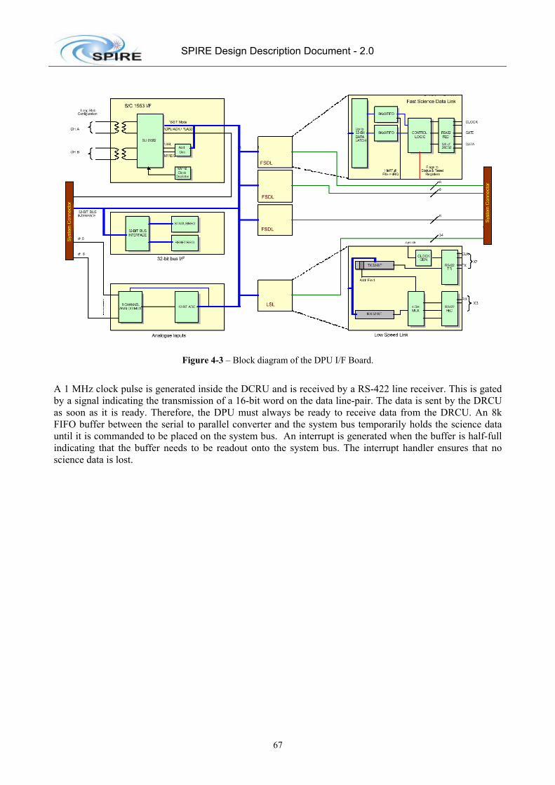
SPIRE Design Description Document - 2.0
67
Figure 4-3 – Block diagram of the DPU I/F Board.
A 1 MHz clock pulse is generated inside the DCRU and is received by a RS-422 line receiver. This is gated by a signal indicating the transmission of a 16-bit word on the data line-pair. The data is sent by the DRCU as soon as it is ready. Therefore, the DPU must always be ready to receive data from the DRCU. An 8k FIFO buffer between the serial to parallel converter and the system bus temporarily holds the science data until it is commanded to be placed on the system bus. An interrupt is generated when the buffer is half-full indicating that the buffer needs to be readout onto the system bus. The interrupt handler ensures that no science data is lost.

SPIRE Design Description Document - 2.0
68
DPU
Data
Bus
D C U G a te
D a ta
C lo ck
R x (1 6 b it )
8 KF IF O
M C U G a te
D a ta
C lo ck
R x (1 6 b it )
8 KF IF O
S C U G a te
D a ta
C lo ck
R x (1 6 b it )
8 KF IF O
Interrupt controller
FIFO half full
FIFO half full
FIFO half full
Figure 4-4 – Fast Science Data Link architecture.
The third interface shown on Figure 4-3 is the Low Speed Link (LSL). This is a bi-directional serial interface between the DPU and the DRCU. The architecture of this link is illustrated Figure 4-5. This link is used to send commands to the DCU, MCU and SCU and to receive housekeeping information from these boards. The Interface Board in the DPU board acts as the controller for this interface with the DRCU boards acting as slaves. Data is transmitted to the individual boards from the system bus. An addressing scheme is used to select the boards intended to receive the commands. A handshake protocol is used to ensure that commands have been received correctly. As the DPU is acting as bus controller, no buffer is required to receive the data sent by the DRCU. The fourth interface shown on Figure 4-3 is the Analogue Inputs. This is used to readout the analogue signals from current and temperatures sensors within the DPU. They are converted to a 12-bit digital values by an ADC chip then placed on the system bus by a FPGA. The fifth interface is to the system Data Bus. The bus has 24 address lines, 32 data lines, 7 chip select lines, read and write lines, clock (20 MHz) and a reset line.

SPIRE Design Description Document - 2.0
69
Clockgenerator
Rx (32 bit)
Tx (32 bit)
Mux
DPU
Data Bus
MCU
SCU
DCU
Rx
Tx
Clk
Rx
Tx
Clk
Rx
Tx
Clk
Address field
Figure 4-5 – Architecture of the Low Speed Link of the DPU.
CPU Board: A block diagram showing the main components of the CPU board is shown in Figure 4-6. A mezzanine board mounted on the main CPU board accommodates some of the components. The microprocessor is a TEMIC TSC 21020 which is the Analog Devices 21020 Digital Signal Processor (DPS) adapted for space applications. The DSP runs at 20 MHz and is capable of peak computational rates of 20 MIPS and 66Mflops and has provision for four hardware interrupts. There is 512k of 48-bit program memory and 512k of 32-bit data memory. A Control FPGA chip is used to provide the following services:
• a system bus control and management, • a local peripheral timing adjustment, • a mezzanine interface, (used to increase the number of available interrupts to eight) • boot logic, • an interrupt manager, • a system watchdog (used to detect lockup of the DPU), • an interval timer.
A 256k 32-bit EEPROM chip is used to store the program. The program is transferred from the EEPROM into the program by the DSP. A schematic representation of the information flow within the DPU is shown in Figure 4-7. On the top left hand side of the Figure, the DPU “Command-handling” electronics receives and interprets commands from the CDMS. Upon successful receipt of these commands, a handshake/acknowledge message is sent back to the bus. The high level commands from the CDMS are processed by the DPU to provide digital driver commands to the DRCU (which acts as the analogue drive/read out electronics for the cryogenic part of the instrument) and are executed in real time. It is the task of the spacecraft to determine the sequence and absolute timing of the commands to be passed to SPIRE. These commands are passed to the DRCU via the

SPIRE Design Description Document - 2.0
70
“Commanding” block in the lower left hand corner of Figure 4-7. Science frames and housekeeping data from the instrument are passed to the “Data Collection” block via the high-speed data interfaces with the DRCU. The housekeeping data (such as instrument temperature, control currents etc.) are monitored by the “Autonomy” block. In the event of a fault condition in the DRCU or in the cryogenic section of the instrument, commands are passed to the DRCU to put the instrument into safe mode. Notification of a fault condition is also passed to the CDMS via the “Packetisation Block” in the top right corner of Figure 4-7. The CDMS then determines if the instrument should be turned off and unlatches the LCL for the DRCU and the DPU as necessary. All data passed from the DPU to the CDMS is formatted according to the ESA Packet Utilisation Standard.
Figure 4-6 – CPU board block diagram.

SPIRE Design Description Document - 2.0
71
CommandsScience Data
HousekeepingEvents
PacketisationCommandHandling
Cmd Ver.
(Verification)
Commanding
DRCUCommands
ScienceFramesHousekeeping
Real-timeDRCU
Commands
Autonomy(Decomposition)
Events Events
Events
Data Collection
Figure 4-7 - Conceptual diagram showing the flow of information within the DPU.
4.1.1.1 Onboard Software The CPU board carries in the PROM the basic software to drive and control the DPU. The tasks the OBS carries out are schematically shown in Figure 4-8.
Telecommands
Telemetry
CDMS OBS
MechanismControl
Unit
Commands DetectorControl
Unit
Commands
Subsystem Control
Unit
CommandsHousekeeping Data
Science Data
Housekeeping Data
Housekeeping Data
Science DataScience
Data
Figure 4-8 - SPIRE DPU On Board Software Context Diagram.
The main functions of the OBS are the:
(i) acceptance of instrument commands from CDMS; (ii) execution of predefined commanding sequences; (iii) instrument health/status monitoring; (iv) implementation of pre-defined procedures on detection of instrument anomalies. When an
anomaly occurs, the OBS either (i) adjusts the instrument operation parameters, and/or (ii) switches the operating mode and/or (iii) activates subsystem redundancy;
(v) science data acquisition and packetisation; (vi) HK data packetisation;

SPIRE Design Description Document - 2.0
72
(vii) transmission of data (science, HK, events and telecommand verification) from the instrument to the CDMS.
In addition, the OBS shall provide the following software oriented functions:
(i) the ability to load, via telecommands, replacement and/or additional software (patches, tables, command sequences);
(ii) self-test and software verification facilities; (iii) the possibility to load and dump part of DPU/DCU memory; (iv) the possibility to write and check EEPROM; (v) the possibility to inhibit these functions during flight operations.
4.1.2 Detector Readout and Control Unit (HSDRCU) The DRC is an electronic unit housed into two boxes: the FCU and the DCU, located between the FPU and the DPU. The DRCU includes the front-end electronics of the following sub-systems:
(i) BDAs, (ii) SMEC, (iii) Beam Steering Mirror, (iv) Cooler, (v) PCAL and SCAL, (vi) Thermometry & Analogue Housekeeping,
The DRCU comprises 4 physical sub-units:
(i) the DCU which includes the detector control, biasing, readout and digitization electronics; (ii) the MCU includes the mechanisms’ (FTS+BSM) control electronics; (iii) the SCU includes the sub-system control electronics; and (iv) the PSU which takes power from the spacecraft power bus and converts it to the required
voltage for the other sub-units of the DRCU. These components are schematically represented in Figure 4-9.

SPIRE Design Description Document - 2.0
73
Figure 4-9 - Schematic block diagram of the DRCU including the interfaces to the DPU and the FPU.
4.1.2.1 Detector control unit (DCU) The DCU acts as the interface between the analogue signals from the detectors and the digital DPU. A schematic drawing of the DCU together with the detector train components in the FPU and the interfaces with the DPU and FCU is shown in Figure 4-10. There are three basic board types used in the DCU; the Lock-in Amplifier (LIA) boards, the Bias Boards and the Data Acquisition and Interface (DAQ + I/F) boards. They are all connected by the motherboard, which forms the back plane for the other boards.

SPIRE Design Description Document - 2.0
74
Figure 4-10 - Schematic representation of the DCU including it's interfaces with the FPU, DPU and FCU.
Bias Boards: Three different biases are provided by the Bias Board, as listed below.
• DC biasing of the JFET modules, • DC biasing of the JFET heaters, and • AC Biasing of the Photometer BDAs, Spectrometer BDAs and the 300-mK Thermal Control
System. Detector Bias Generators: As described in §4.3.4, the detectors are differentially biased with an AC voltage, which is provided by the Bias Generator board. Separate generators are used for Due to the criticality of this component of the detector read out electronics, there is both a prime and redundant board for the bias signals. The amplitude, frequency and phase of the bias signals are all software commandable with the XC-4010-200 FPGA chip on the DAQ + I/F board. This FPGA generates a series of 12-bit words, which correspond to the amplitude of the bias signal. These words are loaded into Analog Devices AD7475A, 12-bit DAC chips that generate the analogue bias signal. These signal are then amplified to the required amplitude with Analog Devices OP-400 operational amplifiers. The characteristics of the bias signal are summarized in Table 4-2.

SPIRE Design Description Document - 2.0
75
Number of channels
48 96 144 24 48
PLW BDA PMW BDA PSW BDA SLW BDA SSW BDA
Signal AC amplitude 10 mV Dark condition Signal DC level 5 mV JFET VOsmax Common mode offset 1 V DC Noise allocation 7 nV/Hz1/2
0.64 pA/Hz1/2 0.05 to 25 Hz
Input capacitance < 100 pF Input impedance > 1 M Base band signal bandwidth 0.03 to 5 Hz
0.03 to 25 Hz 5 Hz
Photometer Spectrometer Thermometry
Input noise impedance > 7kΩ Common mode rejection - 60 dB 30–300 Hz
Table 4-2 – Detector driver electronics specifications.
Figure 4-11 - Back plane connections to the photometer LIA cards. The spectrometer LIA boards are conceptually
indentical.
LIA Amplifiers: The Lock-in Amplifiers are used to read out the AC signals from the detectors and convert them into DC. Each bolometer has a dedicated amplifier. The amplifiers are grouped together in groups of 32 on each LIA board. Figure 4-11 shows the interconnection between the LIA boards on the motherboard. The analogue output from each of the amplifiers is placed on a bus connected to the DAQ + I/F board. Each individual amplifier has;

SPIRE Design Description Document - 2.0
76
(i) a differential input pre-amplifer circuit that uses Analog Devices OP-400 operational amplifier; (ii) an Intersil, DG303A digital switch. This takes the pre-amplified AC signal from the bolometer and
full wave rectifies it using the signal from the bias generators. The switching is signal is phase commandable to compensate for any signal phase change that occurs between the detector and the digital switch in order to maximize the output from the switch;
(iii) an active post low pass filtering circuit that removes the bias frequency and bias harmonic components from the rectified signal. The low pass filter circuit uses two Analog Devices OP-400 operational amplifiers.
These three components are illustrated in Figure 3-25. There are a total of 12 LIA boards; with nine being used for the photometer and three used for the spectrometer. The DAQ + I/F boards: The analogue signals from the 288 photometer channels and the 72 spectrometer channels need to be converted into digital values. To get the required precision, the signals are digitised into at least 19-bit precision. Firstly, the DC offset is removed from the analogue signal. This offset is the three most significant bits of the digitisation. The signals are then passed into an analogue multiplexer before being passed to a 16-bit Analogue-to-Digital converter chip. The conversion of all the photometer channels is performed in less than 6.2 ms; the spectrometer channels in less than 1.2 mS. The digitised signals are then passed to the DPU via the HSDL. The board also manages the LSL link and the commanding of the DCU.
4.1.2.2 Mechanisms Control Unit MCU The MCU controls and monitors the two mechanisms of the SPIRE instrument, viz.:
(i) the Spectrometer Mechanism (SMEC). The control is typically based on a scan at a configurable speed, but can be set-up on the basis of a step position control in case on use of the step and integrate mode of the instrument;
(ii) the chopper and jiggle axis of the Beam Steering Mirror subsystem . The control is a position step control pattern.
The position and rate control of the 3 axes is performed by an Analog Devices 21020 DSP chip using PID control architecture. The MCU software is based on a master scheduler using the principle of time sharing without a specific multi tasking kernel. The tasks to be performed shall be called on the basis of a software interrupt generated by the inner DSP timer. The software interrupt defines the global sampling time (ie the computation cycle) of the DSP tasks at a programmable rate of between 100 and 300 µs. During each cycle, the following tasks are performed :
(i) the SMEC control loop task (ii) the BSM chop control loop task, (iii) the BSM jiggle control loop task, (iv) the communication with the command line and other various internal DSP tasks.
The scan parameters are put in memory for configuration purpose with a command bi-directional serial line. The MCU receives commands from the DPU via a 32-bit, bi-directional serial interface. The MCU also sends three types of data back to the DPU:
(i) H/K Data: which consists of the readout of single variables read by the command line at a rate of about 1 Hz. The H/K variables readout by a get-parameter command from the DPU. The delay between transmission of a H/K readout request and the response is about 500 µs. Typical H/K variables include, mean SMEC scan speed, SMEC control status, SMEC encoder status, Chopper mean position, Jiggle mean position etc.
(ii) Trace Data: The trace data is a buffer in the DSP memory which contains a long data acquisition. The number of trace variables, the sampling time, the length of the data buffer

SPIRE Design Description Document - 2.0
77
are programmable. This buffer can be read off-line, i.e. when the DPU sends a dedicated command for each variable. Typically, the trace data mode shall be used for the scanning of large number of samples for engineering purposes;
(iii) Telemetry Data: The telemetry data is the SMEC time counts between two encoder 2 micron positions and the BSM chop and jiggle positions The telemetry data is transmitted on a fast 16-bit, 1 MHz serial line. The telemetry line is independent of the DSP control and monitoring and is used for the delivery of data related to the detector signals , with a high level of synchronisation.
Physically, the MCU is composed of a motherboard which acts as the back-plane for the with two MAC (Multi-axis Controller) boards, the two SMEC boards a the single BSM board. All these boards have a prime and redundant side. Figure 4-12 shows the schematic block diagram for these boards. The MAC interfaces via two digital interfaces with the DPU. The first link is a bi-directional 32-bit serial interface for the transmission of telecommands from the DPU and the retransmission of acknowledge words back to the DPU. This interface is controlled by a FPGA chip. The commands are then passed to the DSP chip. During normal operation, the DSP cycles at a frequency between 10 kHz and 3.33 kHz through the following sequence:
(i) the SMEC digital PID control algorithm is updated; (ii) the chop stage BSM digital PID control algorithm is updated; (iii) the jiggle stage BSM digital PID control algorithm is updated; (iv) the trace table is updated; (v) any commands from the DPU are uploaded from the FPGA and the acknowledge reply is
sent.
BSM
SMEC
MAC Board
DPU
CommandSerial Link
Interface FPGACommandSerial Link
Command/Parameters
ParametersSystem Status Reply
Temp probe signals
Clock
Telemetry FPGA
SMECDigital
Controller
SMECTrajectory
Profiler
CommandInterpreter
DAC
time betweenpulses
Timer
QuadratureCounter
Synchro/filtering
Sine andCosine0Xingpulses
Telemetry:Encoder pulse deltatime , Positions, HK
TelemetryHigh data
rat eSerial Link
Logics and safety
ChopperPosition
TrajectoryProfiler
ChopperDigital
Controller
DAC
Digital I/Os
T°C Probes
DataMemory
JigglePosition
TrajectoryProfiler
JiggleDigital
ControllerMuxADC
21020 DSP
Data Bus
High RateSerial LinkInterface
Clock
SMECBoard
BSM Board
SMECMotorcoil
pre amplifier
Moire fringesEncoder
AcquisitionElectronics
Moire FringesSensor
LVDT/HomesensorCond.
BSMChopper andJiggle motor
Moire fringessine signals
@0,120,240°
PWR AMP
Magneto-ResistiveSensors
2x PWR AMP
LVDT
LaunchLatch
Switches
//
DAC
Figure 4-12 - Architecture of the MCU.

SPIRE Design Description Document - 2.0
78
The PID algorithm is implemented in software using standard 21020 assembly language without the use of a specific off-the-shelf real time operating kernel. The assembly language is chosen because Analog Devices provides directly specific libraries to produce PID, filtering, arctan computation with a high efficiency and readability. The SMEC is typically required follow a saw-tooth position profile as shown in Figure 4-13. The scan nominally starts from 3 mm before the Zero Path Difference (ZPD) position, through to 32 mm. The absolute position of the mirrors vs. time is required in order to be able to obtain a spectrum from the detector signals. This is done in a two step procedure.
ZPD Position
Start of Scan
End of Scan
0
Start of Ramp
Scientific Scan FlybackPosition
Time
Figure 4-13 - SMEC Scan characteristics.
BSM position sensing: The position of the BSM chop and jiggle stages is monitored via coil inductance. Along with magneto resistive sensing elements.
4.1.2.3 Subsystems Control Unit (SCU) The SCU carries out the following analogue functions:
• Biasing of the sorption cooler recycle heater, • Biasing of the sorption cooler gas switches heaters, • Biasing of the heater on the cooler cold tip • Biasing of the calibrators black bodies, • Measurement and readout of the calibrators temperature • Measurement and readout of cold instrument temperature channels, • Measurement and readout of analogue housekeeping channels, • The switching (on/off) of sub-unit power supplies.
It also carries out the following digital functions:
• The decoding of low level commands from the DPU, • Provide response to low level commands, • The generation of relative timestamps on Telemetry, • Digitization of housekeeping parameters, • Transmission of digitized data (data + hsk + relative timestamp) to the DPU
A block diagram showing the architecture of the SCU is shown in Figure 4-14.
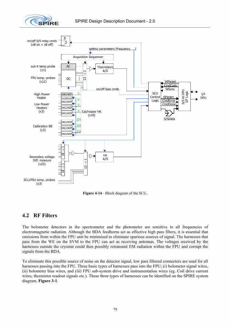
SPIRE Design Description Document - 2.0
79
Figure 4-14 - Block diagram of the SCU.
4.2 RF Filters The bolometer detectors in the spectrometer and the photometer are sensitive to all frequencies of electromagnetic radiation. Although the BDA feedhorns act as effective high pass filters, it is essential that emissions from within the FPU unit be minimised to eliminate spurious sources of signal. The harnesses that pass from the WE on the SVM to the FPU can act as receiving antennas. The voltages received by the harnesses outside the cryostat could then possibly retransmit EM radiation within the FPU and corrupt the signals from the BDA. To eliminate this possible source of noise on the detector signal, low pass filtered connectors are used for all harnesses passing into the FPU. Three basic types of harnesses pass into the FPU; (i) bolometer signal wires, (ii) bolometer bias wires, and (iii) FPU sub-system drive and instrumentation wires (eg. Coil drive current wires, thermistor readout signals etc.). These three types of harnesses can be identified on the SPIRE system diagram, Figure 3-1.

SPIRE Design Description Document - 2.0
80
4.2.1 Subsystem Filters Six filter boxes for the subsystems are located on the spectrometer side of the FPU (see Figure 3-4) for the . They have two 37-way filtered MDM socket connectors on the WE side of the box connected to two 37 way MDM plug connectors on the subsystems side of the box. Type-T Cristek filtered MDM connectors are used for the subsystem. The filter units are attached to the SPIRE optical bench by a blade support structure as shown in Figure 4-53. As the spectrometer cover is placed over the SPIRE optical bench, the outer cover meets with the filter units. The filter boxes are then screwed tightly to the outer cover with a 30 mm bolt spacing and become a part of the RF tight FPU enclosure. The required mechanical rigidity of the filter boxes come from the bolts attaching them to the outer cover. The first natural frequency of the filter boxes is above the required 200 Hz.
4.2.2 Detector and Bias Filters The requirement on the filtering of the detectors is that frequencies from 500 MHz to 10 GHz be rejected to 60 dB. Cristek filtered MDM connectors,l Type M are used for this. The filtering occurs within the connectors in the JFET enclosures. The insertion losses for the Cristek filtered MDM connectors at room temperature and with a 50Ω source and load impedance is shown in Figure 4-15.
Figure 4-15 – Attenuation curves for the MDM filtered connectors used in SPIRE. The detectors use type ‘T’ while the subsystems use type ‘M’.

4.3 Bolometric Detector Arrays
4.3.1 Principle of semiconductor bolometers The SPIRE detectors are semiconductor bolometers. The basic principles of operation are illustrated in Figure 4-16.
Heat sink: Temperature To
AbsorberTemperature THeat capacity C
Thermometer
Thermalconductance
G
Bias current, IRadiant power Q
Figure 4-16 - Principles of bolometer operation.
The bolometer comprises a low heat capacity absorber designed to absorb the incident submillimetre radiation. The absorber is coupled to a heat sink at a fixed temperature To by a thermal conductance, G. Absorbed radiant power, Q, is thermalised in the absorber resulting in an increase in temperature over the equilibrium value in the absence of illumination. A semiconductor thermometer is attached to the absorber. A bias current, I, is passed throughout the thermometer, and the corresponding voltage across the thermometer is measured. The bias current dissipates electrical power P = I2R, which heats the bolometer to an operating temperature T, slightly higher than To. The main performance parameters for bolometric detectors are: Responsivity: S = dV/dQ Noise Equivalent Power: NEP = a(4kTo
2G)1/2 where k is Boltzmann's constant and a is a constant of order 1.
Time constant: τ ~ C/G where C is the heat capacity of the bolometer. For a full account of the theory and practice of semiconductor bolometers, see, for example, Mather (1982), Griffin & Holland (1988), Richards (1998).
4.3.2 SPIRE bolometer performance requirements The combination of good sensitivity and speed of response requires low-temperature operation. The ultimate limit to the sensitivity of the SPIRE instrument is determined by the thermal background power from the telescope. The background power incident on a SPIRE detector is typically a few pW , almost all of which is from the telescope. This corresponds to a background photon rate of ~ 1010 photons per second. Note that

SPIRE Design Description Document - 2.0
82
this is enormously larger than in the case of optical observations. The accurate subtraction of this thermal background is essential if the much fainter astronomical signals are to be measurable. Furthermore, statistical fluctuation in the arrival rate of these background photons creates a fluctuating noise power which represents a fundamental thermodynamic limitation to the sensitivity. For SPIRE, the associated photon-noise limited NEP, NEPph, is a few x 10-17 W Hz-1/2. In order to achieve photon noise-limited performance, the inherent NEP of the detector system must be comparable to or lower than this. The noise of the bolometer itself is a combination of Johnson noise and phonon noise (due to the quantised flow of thermal energy from the bolometer to the heat sink). The instrument performance models described in §6 contain detailed calculations of the background power levels and sensitivity for SPIRE. In addition, the operating modes require time constants of around 30 ms for the photometer detectors and 16 and 8 ms for the two FTS arrays. With current bolometer technology, these sensitivity and time constant requirements can be met by detectors operating at a temperature of around 0.3 K, cooled by a 3He refrigerator.
4.3.3 SPIRE bolometer design and specifications SPIRE will use arrays of semiconductor bolometers developed at Caltech/JPL. Figure 4-17 illustrates the basic detector design. The absorber is a "spider-web" of metallised silicon nitride. This appears as a filled planar absorber to the submillimetre radiation which has a wavelength much longer than the grid spacing. The spider-web structure has high mechanical strength and a low filling, factor providing low heat capacity and immunity to glitches that can be caused by ionising radiation. The diameter of the spider-web is typically a few times the wavelength to be detected. The thermometer is a small (20 x 100 x 300 µm) crystal of Neutron Transmutation Doped (NTD) germanium. This material is highly suited for use in low temperature bolometers as its thermal behaviour closely approaches that of an ideal thermal device, the material displays very low 1/f noise, and the manufacturing processes are highly repeatable and reliable. A wide range of NTD materials are available to tailor the impedance of the device to the desired range for the chosen operating temperature. Large arrays of bolometers can now be made, as illustrated by the array wafer shown in Figure 4-17.
Figure 4-17 - Left: Photograph of part of a SPIRE P/LW (520-µm) array wafer, showing individual spider-web bolometers and lithographed electrical connections. Right: close-up of an individual bolometer. The dark rectangle is
the TBDxTBD NTD thermometer.

SPIRE Design Description Document - 2.0
83
4.3.4 Bolometer readout electronics The resistance of the detector at the operating point is typically 5 MΩ. Lower values make it difficult to avoid being preamplifier noise limited while higher values can pose problems with electromagnetic pick-up and sensitivity to microphonic disturbance. The detector noise is typically 10-20 nV/Hz-1/2, and the noise of the readout amplifier must be of this order or less. With current transistor technology, this requires the use of silicon JFETs, which must operate at a temperature of around 120 K, and must also be located as close as possible to the detectors. This is why SPIRE employs JFET amplifier modules as part of its cold FPU. The essential features of the readout electronics are shown in Figure 3-25. The bolometer is biased (heated to its optimum operating temperature of around 1.3To) by a sinusoidal current bias at a frequency of at least 100 Hz, applied via the 10-MΩ load resistors. The bias excitation is much faster than the thermal time constant, so that bias itself does not produce a temperature modulation. This is preferred over DC bias as it up-converts the signal information to the bias frequency, getting well above the 1/f noise knee of the JFET readout amplifiers. With this arrangement, because of the inherently low 1/f noise of the bolometers, the1/f noise knee of the system can be very low (less than 0.1 Hz).
10 MΩ
10 MΩ
Bolometer~ 5 MΩ
AC bias ~ 100 Hz
JFET power
Differential output to warm amplifier
50 kΩ50 kΩ
~ 100 K300 mK
Figure 4-18 - Bolometer bias and cold readout circuit.
4.3.5 Feedhorns and bolometer cavities The size of a composite bolometer (typically mm diameter) is small compared to the telescope diffraction spot (in the case of SPIRE, with f/5 final optics, the spot size is 2.44λF = 12.2 mm at 500 µm) and the first-pass absorption efficiency of the absorber is only ~ 50%. In order to couple the telescope beam onto the detectors in the array, conical feedhorns are used, with a short section of waveguide at the end of the horn to feed the radiation into a cavity containing the bolometer, as shown schematically in Figure 4-19. The waveguide acts as a low-pass filter as it does not propagate radiation of free space wavelength > 3.4a where a is the radius. For high efficiency, the absorber is located in the centre of the cylindrical cavity with λ/4 spacing between the front of the cavity and a reflecting back-short at the back. The feedhorns are packed in a hexagonal arrangement in the focal plane to fit as many as possible into the area available.

SPIRE Design Description Document - 2.0
84
Siliconsubstrate
at 300
Conicalfeedhorn
Circularwaveguide
λ/4
2Fλ
Metalisedsilicon
nitride web
NTD Gethermometer
mK Figure 4-19 - Left: feedhorn eedhorn and cavity design. Right: photograph of SPIRE P/LW (500-µm) feedhorn array.
Maximum feedhorn aperture efficiency of 70-80% is achieved for a horn diameter close to 2Fλ (e.g., Griffin, Bock and Gear, 2002), corresponding to a beam spacing on the sky ~ 2λ/D, where D is the telescope diameter. The horn restricts the detector field of view, giving a tapered (near Gaussian) illumination of the telescope primary mirror (with an edge taper of approximately 8 dB in the case of SPIRE). Whilst the horns are close-packed in the focal plane, their beams on the sky do not fully sample the image unless the horn diameter is = 0.5Fλ. Several separate telescope pointings are therefore needed to create a fully-sampled image. For the 2Fλ horns 16 pointings are required in principle, as illustrated in Figure 4-20. In the case of SPIRE, the step size is dictated by the shortest wavelength channel (P/SW - 250 µm) and the number of steps is dictated by the longest wavelength channel (P-LW - 520 µm) so that a 64 point jiggle map is needed to achieve simultaneous full spatial sampling in all photometer bands.
Beam FWHM = λ/D
Beam separation on the sky = 2λ/D
Feedhorns adjacent in the focal plane
Figure 4-20 A 16-point “jiggle pattern” is needed to achieve a fully sampled map with 2Fλ feedhorns (for hexagonal
packing the jiggle pattern is slightly different but 16 steps are still required).
The main advantages of feedhorn arrays are:
(i) maximum efficiency for detection of a point source with known position; (ii) well understood horn properties, allowing good control of the beam and reliable design; (iii) good stray light rejection - the bolometer field of view is restricted to the telescope; (iv) good rejection of EM interference - the horn plus integrating cavity act as a Faraday
enclosure; (v) minimum number of detectors for a given total field size.

SPIRE Design Description Document - 2.0
85
The main disadvantages are that the observing modes are complicated (jiggling or scanning) and that the efficiency for mapping is a less than the ideal (Griffin, 2000). This means that the full collecting area of the telescope is not used with maximum efficiency. In order to collect the radiation from a point source with good efficiency, the detector through put must be of the order of λ2. The diffraction-limited beamsize of a telescope of diameter D is approximately θ ≈ 1.2λ/D. The corresponding solid angle on the sky is Ωsky = π(θ/2)2. The throughput (the product of area and solid angle, which is conserved in an ideal optical system) is therefore
AtelΩsky ≈ [πD2/4][π(1.2λ/2D)2] ≈ λ2. The SPIRE photometer uses smooth wall, single-mode feedhorns - the circular waveguide section allows propagation of only one mode (TE11). The corresponding throughput (defined as the area-solid angle product) is exactly λ2. The spectrometer uses multi-mode feedhorns that pass both TE and TM modes.
4.3.6 Bolometer array thermal-mechanical design The design of the SPIRE array units (called Bolometer Detector Arrays, BDA's) is illustrated Figure 4-21. Each BDA unit is split into a 2-K and a 300-mK section. The 300-mK section contains the feedhorns, waveguides, bolometer array wafer and the supporting structure. The 2-K detector structure forms the mechanical interface between the 300-mK structure and the photometer or spectrometer 2-K enclosures. The enclosures are connected via thermal straps to the 1.7-K stage of the Herschel cryostat. The heat load from the 2-K structure to the 300-mK structure of the BDA is minimised by suspending the 300-mK section from the 2-K structure with two pre-tensioned 3000-denier Kevlar cords. Kevlar has high mechanical strength in tension and a very low thermal conductivity at this temperature, and forms gives good thermal isolation between the assemblies. The estimated heat load is less than 1.6 µW per array. The high mechanical rigidity of the Kevlar cord yields a high resonant frequency (> 200Hz).
Figure 4-21 - Left: Bolometer Detector Array module design (not incorporating some superficial modifications to the
design that have been recently been introduced). Right: photograph of a prototype P/LW BDA (without the array filter).
Table 4-3 lists the some of the main design and performance parameters for the SPIRE detectors. .
Filter 300-mK strap attachmentpoint
Kevlar supports
2-K interface flange
Kapton ribbon cables

SPIRE Design Description Document - 2.0
86
Yield > 90% Operating Resistance ~ 5 MΩ Time constant < 32 ms (photometer)
< 14 ms (spectrometer/LW)< 8 ms (spectrometer/SW)
Responsivity 0.4 GV W-1
Detector noise 14 nV Hz-1/2
Efficiency of bolometer-cavity-feedhorn combination > 0.65 Average BDA mass < 0.6 kg Lowest BDA resonant frequency > 200 Hz Total heat load budget on 3He cooler (5 BDAs) < 15 µW Total JFET power dissipation (photometer mode) < 42 mW
Table 4-3 - Main design and performance parameters for the SPIRE detectors.
A more detailed description of the bolometers can be found in Turner et al. (2001), and the design, modelling and performance of the feedhorns is described in Rownd et al. (2002) and Chattopadhyay et al. (2003). Full details of the SPIRE BDA specifications are given in the Detector Subsystem Specification Document.
4.4 JFET units The CMRR of the JFETs is 40dB (Check with Bruce) The functionality of the JFET in the read out electronics of the BDAs is adequately described in §4.3.4 above. The JFET boxes are described here as a sub-system in themselves. Electrically isolated Model U401 Silicon JFETS are used to read out the SPIRE detectors, mounted in groups of 24 on silicon nitride membranes. The contract traces and JFET source resistors are lithographed on the membranes. The JFET modules for the photometer and spectrometer are mounted in separate enclosures (illustrated in Figure 4-22) on either side of the FPU. There are two sets of JFET boxes, one set drives the signals from the photometer detectors and the other set drive the spectrometer detectors. To minimise the signal loss or phase distortion due to harness capacitance, the length of the harnesses between the JFETS and the bolometers needs to be minimised. Hence, the two groups of |JFETs are located on the Herschel optical bench as close to the FPU structure as is practical. Thermal Design: To attain the required noise performance, the individual JFET devices need to operate at around 110K. This poses several challenges to the thermal design of the modules: (i) the surrounding structure is at the same temperature as the Herschel optical bench. The thermal load
from the JFETs to the JFET structure has to be minimised so as to minimise the power used to heat the JFETs. The nominal limit for all the JFETs in a single operating mode is 33 mW.;
(ii) the thermal load from the JFETs to the structure needs also to be limited to ensure that the heat load to the FPU through the detector harnesses is minimised.
High thermal impedance is therefore required between the JFETs and the rest of the structure. This requirement is achieved through the mounting of the devices on thin silicon nitride membranes and low cross section lithographed wires to the individual JFET terminals. The silicon nitride membrane also meets the functional requirement of providing a high resonant frequency.

SPIRE Design Description Document - 2.0
87
Filters identical to the ones described above in §4.2 are inserted on all the inputs to the JFET boxes. Included in the structure of the JFET box is the provision of filter units identical to the ones used inside the FPU to filter the AC bias signals going to the detectors. All the harnesses passing from the JFET units to the FPU are shielded. This effectively enlarges the RF shielding provided by the FPU enclosure to include these shields. The structure is rigidly attached to the Herschel optical bench by four bolts. It is fabricated from aluminium in order not to generate thermal stresses at cryogenic temperatures. The first mode of vibration is above 100 Hz. The structure also has a thermal strap connecting it to Level-2 of the cryostat. The structure is electrically isolated from the Herschel optical bench by Vespel washers.
Figure 4-22 - Front view of Photometer JFET rack. (JFP).

SPIRE Design Description Document - 2.0
88
Figure 4-23 - Rear view of Photometer JFET Rack (JFP) including details of the routing of the back harness.
Figure 4-24 - Exploded view of a single JFET module.

SPIRE Design Description Document - 2.0
89
Figure 4-25 - View showing assembled JFET modules.

SPIRE Design Description Document - 2.0
90
4.5 Mirrors The basic design of the mirrors is the same as the one used for ISO-LWS. The mirrors are made from Al-6061. They all have a standard interface with the structure, i.e. an M8 screw and a pin. Each mirror is machined in a single block of aluminium (diamond cutting). Before the final finishing of the machining process, the mirrors are annealed to remove any residual stresses that may cause distortions at cryogenic temperatures. The screw part of the attachment exerts pressure only on the shoulder part of the mirror, avoiding deformation of the optical surface. The mount of each mirror is located on the optical bench by means of several hollow pins. These pins ensure that in case of dismounting of the mirror, it will be reassembled in the same position. During integration of the mirrors in the SPIRE structure, the mirrors are mounted on brackets. The mirror mounts are designed to have the first natural mode of vibration above 200 Hz. Figure 4-27 below shows a drawing of the CM5 mirror, which is the heaviest one. For the mechanical interface between the mirror mounts and the SPIRE optical bench, the standard technique of using a hollow dowel pin is adopted. The mounting accuracy is nominally within 0.5 arc minute and 0.05 mm linearly. The mechanical interface between the mirror and the mirror mount is illustrated in Figure 4-28. This technique ensures that the rotational and translational degrees of freedom for the mirror are tightly constrained in a repeatable fashion. The finish of the mirrors is to optical quality. This is to permit the alignment of the mirrors to be performed within the optical wave lengths (< 10 nm RMS, specular reflectivity > 80%). The emissivity of the surfaces within the sub-millimetre wavelength is to be less than 1% to minimise the spurious emissions transmitted to the detectors. The specular reflectivity in the same wavelength is in excess of 99%. All the common mirrors, the photometer mirrors and the spectrometer mirrors are listed and briefly described in Table 4-4. The locations of the mirrors with respect to the other optical components are illustrated in Figure 4-29 and Figure 4-30. Information on the optical alignment of the instrument, and details of the corner cubes is found in the FIRST SPIRE: Optical alignment verification plan, (Origne and Dohlen 2000).
Figure 4-26 – Example of mirror mounts.

SPIRE Design Description Document - 2.0
91
MatiÞre RugositÚ
DÚsignation
NumÚro
Contr¶le
Figure 4-27 - Engineering drawing of CM5
Figure 4-28 – Drawing of the Mirror/Mirror Mount mechanical interface.

SPIRE Design Description Document - 2.0
92
Subass'y Mirror Type R or Ry
(mm) CC or Rx
(mm) Shape Dimensions
a x b or dia decenters
[c , d] (mm)
Mass (kg)
CM3 Off-axis asphere
365.963 -0.5095 Rectangular 139x62 [-19.5, 145]
See fig.
0.256
CM4 (BSM) Flat 15x16 0.021
Fore optics
CM5 Toric 294.638 278.418 Rectangular 161x85 [19.5, -1.5]
0.360
PM6 (Pick-off)
Toric -307.49 -359.42 Rectangular 46x27 0.027
PM7 Sphere 330.70 Rectangular 118x101 [0, -1.0]
0.300
PM8 Sphere -286.651 Circular Ø 60 0.056
PM9 Sphere 350.851 Circular Ø 112 0.223
PM10 (Fold mirror)
Flat Rectangular 78x40 [2.5, 0]
0.065
Photometer
PM11 (Fold mirror)
Flat Rectangular 56x53 [0, -2.75]
0.060
SM6 (Pick-off)
Toric 523.79 269.92 Elliptical 9x12 [0, 1.0]
TBD
SM7 (Fold mirror)
Flat Rectangular 40x57 [0, 4.0]
0.044
SM8A, B (Relay in)
Toric 230.34 202.00 Circular Ø 60 0.112
SM9A, B (Collimator)
Sphere 259.50 Special
Ø50
0.074
CC face1 Flat Special
40x60
0.044
CC face2 Flat Special
28x68
0.070
CC face3 Flat Special
28x68
0.070
SM10A, B (Camera)
Sphere 260.00 Special
Ø60
0.112
SM11A, B (Relay out)
Toric 196.99 169.84 Circular Ø 74 [0, 1]
0.194
Spectrometer
SM12A, B (Fold mirrors)
Flat Elliptical 21x16 [-1, 0]
0.050
Table 4-4 – General mirror specifications. The locations of these mirrors are illustrated in Figure 4-29 and Figure 4-30.

SPIRE Design Description Document - 2.0
93
CFIL1
PFIL3
Common Structure
CM3CM3
CM5
PM7
(CM4)
PM6PM8
SOR
SOB
FOB
PFIL2
PCAL
FOR
PDIC1
PDIC2
PDBX
PM9
PM10
PM11
PSW
PMW
PLW
PFIL4SPFIL5S
PFIL4MPFIL5M
PFIL4LPFIL5LSHUT
3HeCooler
CSTR1
CSTR2
CSTR3
CSTR4
BSBR
BSM
CBFL1 PBFL2
Figure 4-29 – Nomenclature for the SPIRE common and photometer mirrors, filters, beam splitters and dichroics.
SBS1 SBS2
SFIL3L
SFIL3S
SDBX
FOB
SLW
SSW
SM7
SM8A
SM9A SM10ASM11A
SM12A
SM8BSM9B SM10B SM11B
SM12B
SMEC
SCAL
SOB
SCCB
SCCA
SOR
FOR
SM6
SFIL4SSFIL5S
SFIL4LSFIL5L
Common Structure
SFIL2
3HeCooler
CSTR3
BSBR
SBFL1 SBFL2
Figure 4-30 - Nomenclature for the SPIRE spectrometer mirrors, filters, beam splitters and dichroics.
4.6 Filters and beam splitters

SPIRE Design Description Document - 2.0
94
Filters are placed at a number of positions within the SPIRE FPU, serving the following functions: (i) definition of the spectral passbands; (ii) minimisation of the thermal loading on the 300-mK, Level-0 and Level-1 stages by rejecting short
wavelength thermal energy; (iii) minimisation of stray light getting to the detectors; (iv) maximisation of the in-band spectral transmission. The filters are implemented as combinations of capacitative and inductive grids formed by evaporation of copper on thin (~ 2 µm) mylar or polypropylene substrates (Lee et al., 1996). Several grids are used in each filter. The grids must be maintained at accurate spacings. This is achieved either by the use of annular rings for vacuum-gap filters or solid dielectric spacers for “hot-pressed” filters. The latter are formed by pressing together a stack of grids and spacers while heating the combination. The result is a solid and robustly self-supporting filter. The SPIRE filter chains are designed on the pessimistic assumption that the telescope surface is perfect even out to UV wavelengths. For complete blocking out to UV, 3 or 4 blocking filters are needed in the chain The filters can withstand multiple cycling to low temperature, and are robust with respect to low temperature vibration. They are unaffected by UV and high energy particle irradiation and have a very low outgassing rate. They are based on technology developed and implemented in the ISO Long Wavelength Spectrometer and also used in numerous ground-based submillimeter instruments. The filters are interfaced to the structure by simple 3-point mounts to ensure that flatness of the grids is not affected by mechanical stress on the support rings.
4.6.1 Photometer filtering scheme The photometer filtering and dichroic scheme is summarised in Table 4-5. The relative positioning of these items is illustrated in Figure 4-29 and Figure 4-30. The two dichoics allow the spectral bands to be directed to the three arrays with high efficiency. CFIL1 A common blocking filter at the entrance to the instrument, designed to block radiation short of
100 µm. PFIL2 A thermal second thermal blocker with an edge at 110 µm at Level-1 providing additional
blocking and located at a baffle. PFIL3 Third blocket with a 170-µm edge located at the Level-0 pupil, at the entrance to the detector
enclosure PDIC1 2-K dichroic with edge at 306 µm. Reflects onto PSW and tramnsmits to PMW and PLW PDIC2 2-K dichroic with edge at 431 µm. Reflects onto PMW and tramnsmits to PLW PFIL4S PFIL5S
Blocker over the PSW array at 300 mK (edge at 200 µm) Short-wavelength edge definer (208 µm) for the PSW array (the long-wavelength edge is defined by the feedhorn waveguide)
PFIL4M PFIL5M
Blocker over the PMW array at 300 mK (edge at 232 µm) Short-wavelength edge definer (303 µm) for the PMW array (the long-wavelength edge is defined by the feedhorn waveguide). Note: this baseline is to leave this filter out as this edge will be defined by the dichroic PDIC1.
PFIL4L PFIL5L PFIL6L
Blocker over the PSW array at 300 mK (edge at 333 µm) Short-wavelength edge definer (431 µm) for the PLW array. Note: this baseline is to leave this filter out as this edge will be defined by the dichroic PDIC2. Long-wavelength edge definer (580 µm) for the PLW array. Note: this baseline is to leave this filter out as this edge will be defined by the PSL feedhorn waveguide.

SPIRE Design Description Document - 2.0
95
Table 4-5 Photometer filtering scheme.
Figure 4-31 shows a prototype photometer 350-µm band filter chain transmission profile on linear and logarithmic plots. The optical and UV transmissions of the individual elements have been measured separately and multiplied together to derive the overall transmission. The horizontal lines on the logaritmic plot indicate the out-of-band rejection requirements, which are comfortably met by the filter chain.
0.00.10.20.30.40.50.60.70.80.91.0
10 20 30 40 50 60 70 80 90 100
Wavenumber [cm-1]
Tra
nsm
issi
on
1.E-27
1.E-24
1.E-21
1.E-18
1.E-151.E-12
1.E-09
1.E-06
1.E-03
1.E+00
1 10 100 1000 10000 100000
Wavenumber [cm-1]
Tra
nsm
issi
on
Figure 4-31 - Transmission characteristics of prototype 350-µm photometer filter chain.
The SPIRE dichroics are implemented as capacitative low-pass edge filters placed at an angle to the beam. To maintain the sharpness of the edge, the angle of incidence is set at < 25o. Figure 4-32 shows typical transmission and reflection profiles for such a dichroic.

SPIRE Design Description Document - 2.0
96
0
0.2
0.4
0 .6
0 .8
1
0 5 10 15 20 25 30 35 40
Frequency [cm-1]
Tra
ns.
Figure 4-32 - Performance of a prototype 15-cm-1 dichroic (red: reflection; blue: transmission).
4.6.2 Spectrometer filtering scheme The spectrometer filtering and beam-dividing scheme is summarised in Table 4-6. The beam dividers are designed to have near 50% transmitivity (T) and reflectivity (R) over the FTS spectral range. The beam splitter efficiencies as viewed by the two detector arrays are 4RT and R2 + T2, both of which should be close to 100%. CFIL1 Common blocking filter at the entrance to the instrument, designed to block radiation short of
100 µm. SFIL2
A thermal second thermal blocker with an edge at 110 µm at Level-1 providing additional blocking and located at a baffle. Identical to PFIL2.
SBS1 Broadband beam divider covering entire FTS range with efficiency 4RT > 90% SBS2 Identical to SBS1 SFIL3S Blocker for SLW array at entrance to Level-0 detector enclosure with 143-µm edge. SFIL3L Blocker for SSW array at entrance to Level-0 detector enclosure with 167-µm edge. SFIL4S SFIL5S SFIL6S
300-mK blocker for SSW. Edge at 168 µm. 300-mK short-wavelength (200-µm) band-defining edge for SSW 300-mK long-wavelength band defining edge for SSW. Note: the baseline is to leave this filter out as this edge will be defined by the SSW feedhorn waveguide. :
SFIL4L SFIL5L SFIL6L
300-mK blocker for SLW. Edge at 233 µm. 300-mK short-wavelength (315-µm) band-defining edge for SLW 300-mK long-wavelength band defining edge for SLW. Note: the baseline is to leave this filter out as this edge will be defined by the SSW feedhorn waveguide. :

SPIRE Design Description Document - 2.0
97
Table 4-6 Spectrometer filtering scheme.
Figure 4-33 shows the measured efficiency of a prototype beam splitter with the SPIRE wavelength range indicated by the shaded region.
0
0.1
0.2
0.3
0.4
0.5
0.6
5 10 15 20 25 30 35 40 45 50 55 60 65 70Wavenum ber [cm -1]
Eff
icie
ncy
2RT
R^2 + T ^2
Figure 4-33 - Measured efficiency of FTS beam splitter prototype.

SPIRE Design Description Document - 2.0
98
4.7 Internal calibrators
4.7.1 Photometer calibrator (PCAL) The purpose of the photometer calibrator is to provide a repeatable signal for monitoring of detector health and responsivity during ground testing and in-flight operation. It is not an absolute calibrator, but may be useful as part of the overall calibration scheme. PCAL consists of a thermal source inside an integrating cavity, the body of which is at (Level-1). The cavity has a light pipe output with a 3-mm diameter aperture. Two identical sources are provided for cold redundancy, both feeding into a single output light-pipe. PCAL has a mass of TBD gm and is located in the Beam Steering Mirror housing behind the beam steering mirror itself (M4), at an image of the system pupil (the telescope secondary mirror). M4 has a central hole of 2.8 mm diameter ,corresponding to the region of the pupil obscured by the hole in the primary mirror, through which PCAL shines. The electrical connections to PCAL and to the BSM are made using a common harness bundle. Because all of the detectors in the photometer arrays view the pupil with near equal efficiency, PCAL produces a very uniform illumination over the arrays (this is an advantage but not a requirement). It is envisaged that the calibrator will be operated in flight at regular but not frequent intervals (at present we assume a notional frequency of once per hour). Operation of PCAL requires the BSM to be switched off and the telescope pointing to be fixed, so that there are no sources of detector power modulation except the calibrator itself. A predetermined current excitation sequence will be applied over a period of ~ 10 seconds, and the corresponding detector signals recorded. The requirement for the brightness of PCAL is that the area:surface brightness product of its emitting aperture shall be ≥ 1% of the area:surface brightness product of the telescope image at the position of M4 (with an assumed telescope temperature of 80 K and emissivity of 4%) over the wavelength range 200 < λ < 700 µm. This will result in an instantaneous S/N of around 500 from the detectors when viewing PCAL. The 150-ms time constant requirement (30 ms goal) for PCAL ensures that it be comparable to or faster than the photometer detectors. A power dissipation requirement of < 2 mW has been adopted to ensure that PCAL operation makes a negligible contribution to the average load of the SPIRE FPU on the Herschel helium tank, and that local heating of the environment will not result when it is operated. The active element of PCAL is an inverse bolometer, similar to a device developed by J. Beeman of UC Berkeley for use in the SIRTF MIPS instrument. The device is also similar in principle to the one used in the ISO Long Wavelength Spectrometer (but with faster speed of response and lower power dissipation). A thin dielectric substrate is coated with a metallic film and thermally isolated from its helium-temperature housing. Electrical contacts allow a current to be passed through the metal film, heating it up to a temperature of 40 K or more. The PCAL emitter is a 1 x 1 mm NiCr coated Mica chip suspended from the 4-K housing by 25-µm diameter brass wires. These wires are soldered on a glass fibre PC board. The baseline emitter architecture and a photograph of a prototype device (in this case with nylon-wire suspension) are shown in Figure 4-34. A typical resistance is 300 Ω, requiring ~ 2.5 mA drive current for 2 mW power. There is a

SPIRE Design Description Document - 2.0
99
1% stability requirement on the constant-current drive, which translates to a comparable stability for the radiant power output. Prototype devices tested to date show that the radiant output requirement can be met comfortably, with some design iteration still needed to achieve the required time constant.
Figure 4-34 - Photograph of PCAL prototype and schematic diagram of PCAL design.
Figure 4-35 shows a schematic of the PCAL housing design. The unit is attached to the BSM structure behind the mirror.
Figure 4-35 - Schematic diagram of PCAL source unit.
1 x 1 mm source Gold tracks onSapphire
Electrical wires andsuspension
Silver epoxy bonds to NiCr film on Mica
Gold-plated copper mount
PCAL enclosure Source inside cover(transparent for clarity)
Electrical connections toBSM wiring harness
Emitting aperture

SPIRE Design Description Document - 2.0
100
4.7.2 Spectrometer calibrator (SCAL) The signal output from one of the FTS detectors represents the difference between the spectra presented at the two input ports. When the FTS is at its zero path difference position, all frequencies are in phase and the signal is at its maximum. Astronomical signals will usually be much smaller than the thermal background from the telescope. To minimise the required dynamic range for detector signal measurement, it is desirable to replicate the telescope spectrum in the second input port. SCAL is required to null the intensity of the interferogram central maximum to accuracy of 5% (goal 2%), and to replicate the dilute spectrum of the telescope to an accuracy of better than 20% (goal 5%) over the 200-400 µm range. The telescope is assumed to be at 80 K and to have an overall emissivity of 4%. It is assumed that the overall emissivity of the system is uncertain by a factor of two, and that the actual value will not be known before launch, and SCAL must therefore have sufficient adjustability to accommodate this uncertainty. SCAL is located at the second input port to the FTS, at an image of the telescope pupil (diameter = 26 mm). The baseline SCAL design is shown in Figure 4-36.
Figure 4-36 - Model of SCAL assembly showing prime and redundant sources and baffle.
Because SCAL is at a pupil, the effective emissivity can be controlled by using a geometrical fill factor. A black (emissivity ~ 1) source that fills only 4% of the pupil area, produces an effective emissivity of ~ 4%. A second, smaller source is provided to accommodate the possibility that the telescope emissivity is lower than the nominal 4%. This source will have an effective geometric emissivity of ~ 2%. Each source consists of a surface-blackened aluminium end cap, with embedded heater and thermometer, on a Torlon strut for thermal isolation. If the telescope emissivity is higher than expected, both sources can be used together to match the telescope
Prime sources
Redundant sources
Baffle
Black 5-K plate
SCAL enclosure

SPIRE Design Description Document - 2.0
101
spectrum. In order to provide full redundancy, a second redundant pair of identical sources is included. A radiation baffle between the sources minimises radiant heating of the passive sources by the active source(s). The plate to which the source assemblies are mounted forms the back plane of a cavity at Level-1 temperature, and is also blackened. SCAL is thus completely non-reflecting, avoiding any potential standing waves that could be set up between the detectors and the calibrator SCAL is required to have stable emission over the timescale of a long FTS observation. The radiant output is required to be stable to within 1% over a period of > 1 hr. A long time constant is therefore desirable. A PID controller, implemented in software is baselined to control the SCAL temperature, and the device shall be designed to have a long intrinsic time constant. However, the cool-down time should not be excessive to prevent emission persisting after the FTS has been switched off (this could, for instance, create stray light problems for photometer observations ). SCAL will be designed to have a warm-up time (to stable operating temperature) of < 15 minutes, and to cool from its nominal operating temperature to < 10 K within 3 hrs (with a goal of 30 minutes). Thermal testing of SCAL prototypes indicates that all of the requirements can be met, and that the spectral matching goal can be met over a wide range of assumed telescope temperature and emissivity. Note that failure of SCAL does not result in loss of the FTS, but the performance for low resolution spectrophotometery would be degraded. Further details in of the PCAL and SCAL device may be found in the SPIRE Calibrators SSSD.

4.8 Beam Steering Mechanism (BSM) The BSM is designed to allow the image of the sky to be positioned and moved across the detector arrays in a controlled manner. Its specifications are fully described in the BSM SSSD. The BSM is mounted on the photometer side of the Spire Optical Bench, with the moveable mirror coincident with an image of the system pupil stop, the Herschel secondary mirror. The BSM must be able to steer the FOV in two independently controlled orthogonal axes. Rotations of the mirror around the Y-axis of the satellite represent “chopping” motions of the FOV while rotations about the Z-axis represent jiggling motions. Various observation modes of the telescope call for simultaneous rotations in both axes. The key specifications of the BSM are summarised in Table 4-7.
Chop stage Jiggle Stage On-sky rotation ± 2 arcminutes ± 30 arcseconds Mirror rotation ± 2° 24’ ± 0° 36’
Frequency 2 Hz (design), 5 Hz (goal) 0.5 Hz (design), 1 Hz (goal) Maximum power dissipation within
FPU 4 mW
Total Mass 1100g Settling time to within 5% of
demand position 10 msec 50 msec
Angular measurement resolution 0.002° True angular position accuracy 0.04°
Angular position repeatability 0.004° Table 4-7 - Key specifications of the BSM.
The BSM is composed of the following components:
(i) Mechanism (BSMm) (ii) Mirror and Photometer calibration source (P-Cal) (iii) Flex-pivots (iv) Gimbal frame (v) Magnetic actuators (vi) Position sensor (vii) Stray light baffle (viii) Thermometer (ix) Structural interface to the SPIRE Optical Bench (BSMs) (x) Warm electronics (BSMe) (xi) Launch-lock device

SPIRE Design Description Document - 2.0
103
Figure 4-37 - General view of the Beam Steering Mechanism with the stray light baffle removed to illustrate the
interior components.
Mirror/Chop Stage: The mirror has a diameter of 32 mm and is machined from a monolithic block of Al-6160. The mirror rotates about the chop axis on an integrally machined shaft. The front reflecting surface of the BSM is machined flat to within 1 µm rms and polished to within 10 nm RMS. The mirror has a specular reflectivity in excess of 99% and an emissivity of less than 1% in the wavelength range 200-670 µm. Perpendicular stiffening ribs machined into the rear surface of the mirror minimises the suspended mass while retaining sufficient in plane stiffness. There is a 2.0-mm diameter (TBC) hole at the centre of the mirror, through which PCAL, the photometer calibration source (see §4.7.1), radiates during operation. This hole is conjugate with the central obscuration of the Herschel telescope. The PCAL source is mounted behind the BSM mirror with a short length of light-pipe coupling the radiation to the aperture at the centre of the mirror. The underside of the mirror is light-weighted and has pockets for the iron plates for the magneto-resistive position sensors. The moment of inertia of the chop stage is 2.1 kg.mm2 and has been minimised to reduce power consumption during chop transitions. Flexure Pivots: The Flexural Pivots allow rotation of the mirror about the Chop and the Jiggle axes while constraining all translational degrees of freedom. These pivots have high radial stiffness, which virtually eliminates unwanted rotation of the mirror due to bearing flexibility. They have minimal static friction to overcome which would greatly complicate the design of the control system and possibly increase the power demand on the actuator. This restoring force provided by the pivots ensures that the mirror returns to the neutral position in the event of power failure to the BSM motors. The mounts for the pivots are designed in such as way so that if the pivots fracture, they are constrained and effectively become journal bearings. This aspect of the design renders this contingency a soft failure mechanism.

SPIRE Design Description Document - 2.0
104
Several different options are open for the final selection of the industrial supplier of the pivots. The main criteria used in the selection are as follows:
1. Spring rate/Pivot Strength: A tradeoff exists between the strength of the pivots and the sping rate. It is desirable that the spring rate of both the chop and jiggle pivots be as low as possible (within other constraints) as a low spring rate will lower the power demanded by the motors. It is also desirable that the pivots be as strong as possible to give as much margin on the launch loads as is possible. It is currently estimated that the spring rate will be approximately 5 Nm/° for the jiggle stage and 0.6 Nm/° for the chop stage and the design loads of approximately 200 N and 25 N respectively. The jiggle stage must be much stronger than the chop stage as the suspended mass is proportionately higher.
2. Material: The flex pivots must take the forces generated by the accelerations imposed on the suspended components of the BSM during launch. The BSM will be at cryogenic temperatures during launch which renders some materials brittle. In particular, grades 420/429 Stainless Steel which are commonly used in flex pivot construction become brittle at cryogenic temperatures. Inconel 718 does not suffer from this problem and is baselined as the material to be used in the BSM flex pivots.
Jiggle Stage: The jiggle stage is in the form of a split frame split and clamps together around the flex pivots. To balance the jiggle stage the framework in the opposite corner to the coils of the actuator has been made solid. This also increases the stiffness of the structure. This structure carries the chop stage, and is inevitably heavier. Since the amplitude and frequency requirements in this axis a stiffer flexures pivot is used for increased strength and reliability. Position sensors for the chop axis are mounted on the jiggle stage, which means flexible cable connections are required, unlike the jiggle stage position sensors, which mount directly on the non-moving housing. An alternative to this may be to place the chop axis sensor also to the housing and compensate for the movement in the jiggle axis in the look up table using this in conjunction with the jiggle axis position. The gimbal frame is fabricated from Al-6061.
Figure 4-38 - Chop (shown in grey) and Jiggles stages of the BSM.
BSM Motors: The magnetic actuators are located at the edge of each stage of the BSM. There is a primary and a redundant motor for each axis. The estimated power consumption is 0.4 mW when chopping at 2Hz with maximum amplitude and an average power consumption of 1.6 mW when jiggling at 1 Hz with maximum amplitude. Depending on implementation, the motor for a single axis will either have:

SPIRE Design Description Document - 2.0
105
(i) the prime coil on one side of the rocker beam and the redundant on the other, leading to an unbalanced load but a more rugged coil, or
(ii) a balanced set of coils with the prime and redundant motor coils wound onto the same bobbin. The coils may be potted (encapsulated) if required, and will certainly require extensive magnetic shielding and strong thermal linking to the thermal straps. All the motor coils mount directly to the BSMs, i.e. the chop stage air gaps must be slightly over-size to accommodate chopping whilst in various jiggle modes. A prototype coil is illustrated below in Figure 4-39. The prototype has copper windings. The flight version of the motor will have Aluminum windings, which is more efficient and dissipates less power into the structure.
Figure 4-39 - Prototype BSM motor.
Position sensors: These sensors are Infineon (ex-Siemens) FP 212 L100-22 differential field plates that sense the position of soft iron pieces in the moving parts. The sensors are dual InSb/NiSb magneto-resistive elements, biased with a permanent magnet and forming part of a bridge circuit. As the position of the gimbal frame moves relative to the position of the sensor, the resistance of the element changes in proportion to the displacement. The sensor is connected in a Wheatstone bridge configuration driven by a constant current source. Hence, the voltage measured across the bridge is proportional to the displacement of the mirror.
Figure 4-40 – Schematic drawing of the Infineon magneto-resistive position sensor.

SPIRE Design Description Document - 2.0
106
Position sensors for the chop axis are mounted on the jiggle stage, which means flexible cable connections are required. The jiggle stage position sensors mount directly on the non-moving housing and do not require these flexible wires. Stray light baffle: Parasitic losses in the actuators, electronics and wiring may cause the temperature of some of the items mounted on the BSM to rise above the 4 K temperature of the Level-1 enclosure. Any radiation emitted from these items must be shielded from the detector arrays. This is achieved through a baffle made from 0.25-mm thick (TBC) Al-6160 (TBC) placed over the components and around the mirror. The baffle fits tightly around the mirror allowing full movement without interfering with the primary beam.
Figure 4-41 - View of the BSM with the stray light baffle covering the electrical components.
Structural interface to SPIRE Optical Bench: The mirror needs to be accurately mounted on the SPIRE optical bench. The mounting interface is shown below.

SPIRE Design Description Document - 2.0
107
Figure 4-42 - Mechanical interface drawing between the BSM and the SPIRE optical bench.
Electrical connector: Two 37-way MDM connectors (one prime and one redundant) accommodates all electrical connections to the BSM and the PCAL device. These connectors are located on the mounting frame. Launch-lock device: During the launch (and operation) of Herschel, failure the BSM Flexure Pivots could result in the mirror being fixed in an undesirable off-axis position. The spectrometer functionality is particularly susceptible to this failure mode - if the BSM gets stuck at one extreme of its angular range, then the field of view of the FTS detectors could be projected outside the SPIRE field of view resulting in loss of the spectrometer. To prevent this from happening, a launch lock device is incorporated into the BSM. This device is a solenoid-driven locking device that reduces the maximum travel range of the Chop and Jiggle axes. During launch or in the event of failure of one or more of the Flexure Pivots, the launch lock solenoids can be energised, constraining the mirror to point ± 1”(TBC) in each axis of the telescope boresight resulting in a soft failure mode. The state of the launch lock solenoid is monitored by a prime and redundant micro-switch. Figure 4-43 shows the location of the launch lock on the back of the BSM. This figure also illustrates the

SPIRE Design Description Document - 2.0
108
Figure 4-43 – View of BSM mounted on the SPIRE Optical Bench and the location of the launch latch device.
Control system: The BSM has a prime and redundant electrical interface with the FCU to provide the necessary feedback control of the mirror-pointing angle. The position of the mirror is controlled via a PID algorithm which is part of the OBS of the MCU. The control scheme treats each rotational axis of the mirror independently of the other. More detail on the hardware implementation of the actuator control and power system is described in §4.1.2.2.
4.9 Spectrometer Mechanism The Spectrometer mirror MEChanism subsystem (SMEC) controls the movement of the rooftop mirrors inside the SPIRE spectrometer. The movement of the mirrors causes there to be an optical path difference between the two beams that enter the spectrometer 2-K detector box. The critical performances of SMEC are the mirror velocity and its stability, the mirror movement around its travel axis and the required accuracy of the mirror position measurements.

SPIRE Design Description Document - 2.0
109
fr-asyz106/05/99fr-asyz106/05/99fr-asyz106/05/99
Figure 4-44 - CAD drawing of the link mechanism used for the SMEC.
Figure 4-45 - Solid model of the SPIRE FTS Mechanism.
4.9.1 Requirements on the mirror mechanism The design of the FTS spectrometer (see §3.4.2) means that there is an effective folding of the optical path difference of a factor of four between the actual movement of the mirror mechanism and the change in the optical path difference (OPD). The required resolution of the spectrometer is for a maximum ∆σ = 0.4 cm-1
at all points in the field of view with a goal of reaching 0.04 cm-1 for at least point sources viewed on axis. There is a further requirement that the systematic noise induced by the movement of the mirrors will not

SPIRE Design Description Document - 2.0
110
prevent low resolution spectroscopy down to at least ∆σ = 2 cm-1. The goal resolution imposes a maximum change in the OPD of ~ 12 cm or 3 cm in actual mirror movement. In order to Nyquist sample the interferogram at the highest frequency present in the optical band (50 cm-1) , the optical path difference must be sampled every 20 microns, or every 5 microns of actual mirror movement. The most efficient method of operating an FTS is the so-called rapid scanning method. Here, the mirror is kept in constant motion while the signal and mirror position are sampled. This method of operation effectively transforms the optical frequency to audio frequencies by the relationship f = vopdσ. Where f is the detection frequency, vopd the rate of change of the optical path difference and σ the optical frequency. The maximum OPD velocity required will be determined by the frequency response of the detectors. For an assumed detector response of 20 Hz the maximum vopd will be 0.4 cm/s or 0.1 cm/s in actual mirror speed. In fact some “head room” may required in case of problems with microphonic interference so the maximum velocity requirement on the mirror mechanism has been set at 0.2 cm/s. I
Figure 4-46 - Views of the engineering model of the SMEC.
In order to further improve efficiency, the interferograms can be taken “single sided”. That is only a short movement is needed on one side of the zero path difference (ZPD) to enable the position of the ZPD to be established and as long a distance as necessary is scanned beyond that to achieve the required resolution. As in the photometer, the signal in the recorded interferograms will be dominated by the telescope emission. The shape of the optical pass band means that the rate of change of the signal is greatest over the scan region close to the ZPD (Figure 4-48); that is at low resolution. In order to fulfil the requirement on the low resolution performance of the spectrometer it is necessary to have good control of the variation in the velocity and knowledge of the mirror position over the scan range close to the ZPD. Further away from the ZPD the requirement is less strict as the rate of change of the signal is much reduced. These scientific and operational requirements impose the following baseline performance on the FTS mirror mechanism or SMEC:
(i) maximum mirror travel required (w.r.t. the ZPD position): – 0.32 to +3.2 cm; (ii) minimum measurement interval of 5 µm is required; (iii) required mirror position measurement accuracy 0.1 µm over +- 0.32 scan range and
0.3 µm thereafter; (iv) the mirror velocity shall be within 0.001 cm/s r.m.s. within a band width of 0.03 to
25 Hz over the entire scan range; (v) additionally movement of the mirrors must not impose any translation or rotation on
the optical beam such as to affect the fringe visibility in the recorded interferogram.

SPIRE Design Description Document - 2.0
111
ZPD Position
Start of Scan
End of Scan
0
Start of Ramp
Scientific Scan FlybackPosition
Time
Figure 4-47 - Definition of a typical scan trajectory for the SMEC.
4.9.2 Control System and Readout The baseline design of the spectrometer is that it should be operated in “rapid scan” mode with a constant mirror velocity and the time at which each position is passed recorded. The mirror movement will be controlled by a digital feed back loop that uses the time between successive pulses from the optical encoder to control the speed of the mirrors. In order that the mirror velocity jitter in the signal detection band (essentially 0.03-25 Hz) does not affect the signal to noise ratio achieved, the feedback loop will be operated at about 2 kHz. The digital feedback loop is implemented using the TEMIC TSC21020 digital signal processor which is also used as the CPU in the DPU. The detectors could be read out in one of two methods given the encoder type we plan to implement: Position sampling with synchronised detector readout. In this technique, the mirror position pulse is used to trigger the readout of the detectors. The time taken to readout the detector array will need to include any possible uncertainty in the time interval between positions due to the uncertainty in the mirror velocity. This method has the advantage that each frame will be recorded at a known mirror position within the uncertainty of the mirror velocity from one position sample to the next. This means the interferograms can be safely co-added with no need to interpolate the data onto a common position grid. The disadvantage of this method is that it requires both a synchronisation pulse from the mirror drive electronics to the detector read-out electronics (and therefore makes the electronics more complicated) and a higher readout rate for the detectors. Time sampling. Here the time of each pulse from the position sensor is recorded and the detectors are independently sampled; with perhaps a start pulse at the start of the scan to synchronise the readout. The advantage of this technique is that it is simpler to implement in the electronics and will be less prone to operational difficulties associated with timing between the position readout and detector readout. The disadvantage is that, because of the uncertainty in the mirror velocity and any hysteresis or scan-to-scan variability in the positioning of the mirror, the detector readouts will have to be interpolated onto a common position grid before co-addition of the interferograms. In practical terms, this will probably prevent on board co-addition of the interferograms and the mirror scan speed will therefore have to be adjusted to allow the data sampling rate to fit within the 100 kbs telemetry bandwidth available for the Herschel instruments. After an assessment of the implementation of the two methods in the electronics system for the SPIRE instrument, it was decided to adopt the time sampling method as the default operating mode.

SPIRE Design Description Document - 2.0
112
4.9.3 The cryogenic mechanism (SMECm) The SMECm is the mechanism which moves the mirrors. The mirrors are considered a part of SMECm. Basically, the movement of the mirrors is a translation only, obtained through the action of a linear actuator. The mechanical design is based on a prototype Goddard Space Flight Center design for a balloon project (Figure 4-44 and Figure 4-46). A base plate supports the mechanism and is mounted on the SPIRE Optical Bench. On the base plate are mounted the fixed part of the actuator and the optical encoder. A moving plate supports the rooftop mirrors and the rule for the optical encoder. The base plate and the moving plate are linked by four "legs", each of which has two arms; one linking the base plate and the intermediate moving plate, the other linking the intermediate moving plate and the moving plate. The articulations at both extremities of the legs use flex pivots. The stiffness of the articulation is very low to keep the actuator power consumption within the specified limits. Consequently, for SPIRE, a launch latch item is added to allow the mechanism to sustain the launch vibrations without damage. The latch is placed between the base plate and the mirror moving plate.
4.9.4 Position measurement For the position measurement system, a Heidenhain LIP interferential linear encoder is used over the complete travel range of the mirror with a linear variable differential transformer (LVDT) transducer implemented over the movement range around ZPD as a redundant device. The LVDT also provides absolute position measurement close to the ZPD, unlike the optical linear encoder, which only provides relative position information. LVDT devices have already flown on many previous space experiments and were used cryogenically on the ISO LWS grating mechanism. Cryogenic tests indicate that the Heidenhain encoder may be used at liquid helium temperatures with only minor modifications to the optical head. The optical encoder will have a resolution of 0.1 µm or better and gives a “pulse” as each position is passed rather than an absolute distance measurement. The encoder will be fitted to the outside of the mirror carriage. Measuring the position at a distance from the signal beam imposes stringent requirements on the “nodding” movement of the mirror mechanism, possibly stricter than those imposed by the optical requirements of the spectrometer. The actual value of the requirement will depend on the final configuration of the flight optical encoder and the final carriage design.
4.9.5 The preamplifier (SMECp) Due to the loss of current on the output signals of the optical encoders when they are cooled down to 4 K, a preamplifier is necessary. The electronic components (JFETs, etc..) are implemented on a card integrated in a separate box on the SPIRE structure. The temperature of the components is set around 100 K. The driving and control of the SMEC is carried out by the SMEC and MAC boards in the MCU.

SPIRE Design Description Document - 2.0
113
Figure 4-48 - Simulated spectrum of the 80 K telescope seen through the SPIRE FTS with representation optical
filtering. The black line is before applying the frequency response of the detectors the red line after. Note the much larger rate of change of the sign
4.10 FPU structure A general view of the FPU structure is shown below in Figure 4-49. The FPU is mounted on the Herschel Optical Bench (HOB) by a three point, isostatic mounting scheme comprising of a single Cone and two A-Frame Supports. These three supports provide a rigid mount for the FPU to the Herschel Optical Bench while allowing for differential contraction between the instrument and the HOB during instrument cool-down. Three main structural elements are mounted off the supports, viz.; (i) the SPIRE Optical Bench, (ii) the Photometer Cover and (iii) the Spectrometer Cover. All subsystems within the FPU are mounted on the SPIRE Optical Bench (with the exception of the instrument harness connectors, the Shutter and the instrument thermal strap interfaces with the Level-0 straps). Figure 4-49 illustrates the coordinate system used in for the SPIRE structure and the main components of the FPU structure. The Spire Optical Bench is machined from a single block of Al-6061 approximately 675 mm long (aligned with the Spacecraft Z axis, See Figure 2-2) by 410mm high (aligned in the X axis) and 50 mm thick. All optical components of the spectrometer are located on the +Y side of the SOB while all the components of the photometer are located on the –Y side. The mass of the SOB is minimised by machining ribbed pockets (nominally 70 x 70 mm) on both sides. The structure has the following set of general requirements:
1. The structure must mechanically support and positively locate the subsystems mounted inside the FPU.

SPIRE Design Description Document - 2.0
114
2. The structure must meet the mass budget allocation of 9884g. 3. The structure must provide the correct thermal isolation between the various temperature stages of
the instrument. 4. The structure must provide adequate EM shielding and stray-light shielding to the photometer and
spectrometer such that the detectors see no detectable spurious EM power. 5. The structure must allow for simple integration and de-integration of the structure and FPU
subsystems.
These requirements are the means by which they are met are discussed below.
Figure 4-49 - General view of the FPU and the Herschel coordinate system. Only one A-Frame Support can be seen in
this view. The second A-Frame is located in a similar position on the Spectrometer Cover.

SPIRE Design Description Document - 2.0
115
4.10.1 Mechanical Requirements The main structural loads imposed on the FPU are those arising from the acceleration and vibration loads seen during launch. The various qualification acceleration levels at the interface between the Herschel Optical Bench and the FPU are set out in the IID-A. These are quoted below for in formation only. Interface load Axis Level
Longitudinal 20g Quasi static acceleration (Case 1) Lateral 2 Longitudinal - Quasi static acceleration (Case 2) Lateral 14g
Sine Longitudinal (5-40Hz) 20g Longitudinal (40-100Hz) 10g Lateral (5-100Hz) 14g
Longitudinal /Lateral (20-100Hz) + 6 dB per octave Longitudinal /Lateral (100-300Hz) 0.05g2/Hz
Random1
Longitudinal /Lateral (300-2 kHz) - 6 dB per octave
Table 4-8 - General interface acceleration loads for the FPU and JFET Boxes. Taken from the IID-A for information only.
To ensure that there is no serious vibrational energy absorbed into the structure during launch, there is also a requirement that the first natural frequency of the structure has to be greater than 100 Hz in both the longitudinal and lateral directions. Over and above this, it is desirable that the structure be as stiff as is practical so that the interface accelerations for the various subsystems mounted off the common structure be as close to those listed in Table 4-8. A finite element model was constructed of the entire instrument to confirm the structural integrity of the structure and the various subsystems under the launch loads listed above. This model indicated a positive margin of safety for yield, ultimate and buckling failure. The first mode of vibration was identified at 136 Hz.
4.10.2 Thermal Isolation Requirements The structure of the instrument is designed to operate at three temperature levels, which gives three passive heat load budgets for the structure. These three budget allocations are listed in Table 4-9 below.
Passive Heat Load Budget Allocation Level-2 to Level-1 6 mW Level-1 to Level-0 1 mW
Level-0 to 300-mK Strap and stray-light baffles
1.6 µW
1 Several notches in the qualification spectrum may be requested in order to meet the structural requirements of the entire instrument.

SPIRE Design Description Document - 2.0
116
Table 4-9 - Thermal budget allocations to the structure taken from SPIRE Thermal Configuration Control Document for information only.
Level-2 to Level-1: The SPIRE Optical Bench, Photometer and Spectrometer covers, BSM, FTS, Sorption Cooler, Mirrors, Filters, Shutter and Calibrators are all intended to remain at the Level-1 temperature (approximately 4 K). Heat will be conducted from the Herschel Optical Bench (Level-2; approximately 10 K) through the FPU supports to the Level-1 structure. The harnesses will also contribute to this budget allocation. The mechanical supports designed for this interface are shown below in Figure 4-50. These supports are particularly difficult to design as they have very stringent and competing requirements on thermal isolation (pushing for a slender design) and mechanical rigidity (pushing for a heavier design). Thermal and mechanical tests have been carried out on the A-Frames which indicate that each of these competing requirements have been met.
05-Apr-00 14:40:38I-DEAS Master Series 7 : SimulationDatabase: /Adam/Spire/Blade_Mount/triangle-final.mf1 Units : SIView : No stored View Display : No stored Option
Task : Post Processing Model/Part Bin: Library1Model: Fem1 Parent Part: triangle blade 2
Figure 4-50- FPU/HOB interface A-Frame and Cone Supports.
The material used in the construction of these supports is Stainless Steel. This was chosen for its high ratio of Young’s Modulus to integrated thermal conductivity between 4 K and 10 K. It should be noted that Titanium alloy TaV6 has a superior figure of merit at lower temperatures. Carbon Fibre could also be used for these supports but the complexity of Carbon Fibre design and development precluded this option. Level-1 to Level-0: This thermal interface is between the Spectrometer and Photometer Detector Boxes and the SPIRE Optical Bench. It is similar to the interface between the FPU and the HOB in that there are competing thermal and mechanical design requirements. A similar solution has been adopted of an isostatic mount with a single Cone and two A-Frame Supports.

SPIRE Design Description Document - 2.0
117
Figure 4-51 - Thermal isolation between Level-1 (SOB) and Level-0 (Detector Box).
Level-0 to 300-mK Architecture: The Bolometer Detector Arrays used in SPIRE work most efficiently below 300-mK A thermal strap between the cold tip of the sorption cooler that runs to a bolted interface with each of the BDAs provides the cooling necessary to achieve these temperatures. (Note: The passive heat load budget allocation to the 300-mK components of the Sorption Cooler and BDAs are held by the respective subsystem providers. The budget allocation to the support structure of the thermal strap is held by the structure.) The strap is thermally isolated from the Detector Boxes by a Kevlar string up. This part of the design is very challenging as the random vibration loads within the detector boxes are very high and failure of the suspension system could result in a thermal short of the 300-mK system and loss of the SPIRE instrument.
4.10.3 Stray light and RF shielding The detectors on SPIRE are extremely sensitive to stray light and spurious electromagnetic radiation. The structure utilises two main techniques to shield the detectors and the read-out electronics from this interference; (1) RF tight joint configuration, and (2) Stray light baffling.
4.10.3.1 RF-tight joint Design When an electric field impinges on a conducting surface, such as the FPU cover, electric currents are induced immediately below the surface that create electric fields that tend to cancel out the incident fields. This effect accounts for most of the electromagnetic shielding of a metallic enclosure. When these currents are impeded from flowing, the structure is unable to cancel out the waves and they will re-radiate into the enclosure. One of the most frequent occurring disruptions to the current flow within an enclosure is at joints between different panels, in fact, a poorly designed joint will act as a slot antenna. This undesirable effect can be minimised by incorporating the following features in the joints in the enclosure.
a. Bolt spacing: The bolt spacing has two main effects. Firstly, a small bolt spacing will increase the clamping force on the joint. A high clamping force will help in ensure that good electrical contact is made between the two interface surfaces. Secondly, bolt spacing delimits the maximum length of any potential gap between the two interface surfaces which reduces the maximum wavelength that can penetrate into the FPU. A maximum bolt spacing of 30mm has been used on SPIRE which is consistent with good EMC practice.
b. Joint quality: The better the dimensional tolerancing of the joint, the better will be the electrical contact between the two halves of the joint. The joints on SPIRE have been toleranced accordingly.

SPIRE Design Description Document - 2.0
118
c. Labarinth: The provision of sharp edged corners around which any stray light or RFI has to reflect greatly assists in improving the performance of the enclosure. Any radiation entering the FPU has to be reflected around at least four corners. The details of this joint can be seen in Figure 4-52. This join design is also effective in preventing the ingress of stray light.
Figure 4-52 - RF and stray light tight joint design used in the FPU.
4.10.4 Alignment requirements The optical components are located on the bench by hollow dowel pins and 8-32 UNC screws provide positive the mechanical attachment. The SOB is manufactured and toleranced in such a way so that the position of the components located on the bench are in the correct position when the bench has undergone the contraction during cooling from room temperature to the nominal operating temperature of 4K. Mirror mount PM6 in the photometer and SM6 in the spectrometer have provisions for remachining to correct any misalignments.

SPIRE Design Description Document - 2.0
119
Figure 4-53 - Details of the mounting of the enclosure for the filtered MDM connectors.
4.10.5 Thermometry Lakeshore, Cernox CX-1030 thermistors are located throughout the FPU. Figure 4-54 shows the dimensions of these thermistors.
Figure 4-54 - View of the Lakeshore, Cernox SD hermetically sealed RTD thermometers.
Location Acronym Temperature
Range Resolution Accuracy
PHOT Level 0 box T_PL0_1 1 K -10 K 2 mK 2 mK FPU SOB/BSM I/F T_SOB_1 3 K - 300 K 10 mK 10 mK Optical sub-bench T_SUB_1 3 K-100 K 25 mK 25 mK Input Baffle T_BAF_1 3 K-100 K 10 mK 10 mK SMEC Mechanism T_FTS_1 3 K - 20 K 10 mK 10 mK SMEC/SOB Interface T_FTS_3 3 K - 100 K 25 mK 50 mK

SPIRE Design Description Document - 2.0
120
SPEC Calibrator 4% T_SCL4_1 10 K - 80 K 5 mK 5 mK SPEC Calibrator 2% T_SCL2_1 10 K - 80 K 5 mK 5 mK SPEC Calibrator Structure T_SCST_1 10 K - 100 K 10 mK 10 mK Cooler Sorption Pump T_CPMP_1 1.5 K - 50 K 0.5 K 1 K Cooler Evaporator T_CEV_1 0.25 K - 10 K 0.1 mK 5 mK Cooler Pump heat switch T_CPHS_1 1.5 K - 25 K 0.5 K 1 K Cooler Evap. Heat switch T_CEHS_1 1.5 K - 25 K 0.5 K 1 K Cooler Shunt T_CSHT_1 1.5 K 10 K 0.1 K NA BSM Mechanism T_BSM_1 3 K - 20 K 10 mK 10 mK SPEC JFET chassis T_FTBS_1 3 K - 100 K 25mK 50 mK PHOT JFET box T_FTBP_1 3 K - 100 K 25 mK 50 mK SPEC level 0 box T_SL0_1 1K – 10 K 2 mK 2 mK
Table 4-10- Location and details of the FPU thermometry.
4.11 Helium-3 Cooler
4.11.1 Introduction The detectors used in the SPIRE BDAs must be cooled down below 300 mK to perform correctly. This is done by a 3He sorption cooler. This sub-Kelvin sorption cooler relies on the capability of porous materials to adsorb or release a gas when cooled or heated. Using this physical process, one can design a compressor/pump that controls the gas pressure in a closed system, condensing liquid at an appropriate location and then performing evaporative pumping on the liquid bath to reduce its temperature thereby providing cooling to a piece of equipment. The total amount of cooling delivered by such a cooler is dependant on (i) the mass of liquid 3He condensed within the evaporator, (ii) the latent heat of evaporation of the 3He at the temperature of the evaporator and, (iii) the parasitic loads to the cooler. The cooler has no moving parts, is vibrationless and is designed to be self contained and compact with high duty cycle efficiency. A summary of the principal design characteristics of the cooler used in SPIRE is presented in .
Cooler cold tip temperature 290 mK (at design conditions) Net heat lift 10 µW (at design conditions)
Parasitic heat loss Less than 12 µW (at design conditions) Hold time More than 48 hours (at design conditions)
Recycle time Less than 2 hours 3He charge 6 litre at STP
Recycle energy (energy dumped into Herschel cryostat during recycle)
Less than 860 J per cycle
Cooler mass 1680 g Volume 228.5 x 100 x 100 mm
First natural frequency Higher than 120 Hz Cold tip temperature fluctuations Less than 10 µK.Hz-1/2 in a frequency band from 0.1-10 Hz
Ultimate temperature 264 mK Cold tip drift requirement 0.1 mK/h
Table 4-11 - Principal cooler design characteristics.

SPIRE Design Description Document - 2.0
121
4.11.2 Cooler components The cooler hardware comprises five main components;
(i) the sorption pump (SP), (ii) the evaporator (EV), (iii) the thermal shunt (TS), comprising a thermal link between the pump tube and the
cryostat level 0, and two gas gap heat switches connecting the sorption pump and the evaporator to Level 0 (HSP and HSE respectively),
(iv) the sorption pump (SP), and (v) the support structure (SST).
These components are labelled on Figure 4-55, which is a view of the entire cooler assembly without the extra structure used to mount the cooler to the SPIRE optical bench. A pumping line connects the sorption pump and the evaporator. The sorption pump, the evaporator, the thermal shunt and the pumping line are assembled to form a single component, which is the actual “heart” of the cooler. This component is held within the support structure, which provides firm mechanical support (launch environment) while minimising any parasitic conductive load on the cooler (low temperature environment).
2-K I/F
Kevlar Suspension
Sorption Pump (SP) Thermal
Shunt (TS)
Evaporator (EV)
Pump tube
Support Structure (SST)
Figure 4-55 - Illustration of the 2-K cooler without cooler to SPIRE optical bench mounting structure.
The heat switch of the sorption pump is coupled to Level 0 of the Herschel cryostat via a dedicated thermal strap that passes through the wall of the FPU. Similarly, a second thermal strap couples the thermal shunt and the evaporator heat switch to Level-0 of the cryostat. Ohmic heaters are located on (1) the sorption pump, (2) the sorption pump heat switch and (3) the evaporator heat switch. Each heater comprises two RLR/2H3 402Ω Vishay metal film resistors connected in series. For each of these devices there is a prime and a redundant heater independently powered and controlled giving a total of six heaters. Cernox thermistors similar to those used elsewhere in the instrument (see §4.10.5) are used to monitor the state of the cooler. They are mounted on (1) the sorption pump, (2) the evaporator; (3) the evaporator and (4) sorption pump heat switches and on (5) the thermal shunt. There are both prime and redundant thermistors on each of the above devices giving a total of ten sensing elements. Thermometry is the only means used to sense the state of the cooler during flight; hence important state

SPIRE Design Description Document - 2.0
122
parameters such as the residual mass of 3He in the evaporator must be inferred from this data along with ground calibration data and onboard software. A prime and a redundant harness connect the cooler to the filter boxes. The cooler has a 37-way MDM plug for each of these harnesses. The cooler is controlled and powered by the FCU. This hardware is described in §4.1.2.3. The associated software is described in §4.1.1.1. Tight specifications on the drift and stability of the cooler cold tip temperature are placed on the cooler and associated control electronics. It is currently not known if these stability requirements will be able to be met during cold AIV and during flight. Provision has been made to incorporate a NTD Germanium thermistors similar to those used in the SPIRE BDAs at the cold tip along with an ohmic heater element. The temperature of the cold tip would be monitored by the thermistors and a control algorithm incorporated into the SCU to modulate the power delivered to the heater element. The power dissipated by the heater element would, of course represent a parasitic heat load to the cooler and would reduce the cooling capacity available to the detectors. This scheme would therefore only be implemented if the system could not meet the temperature stability requirements. The hardware will not be implemented in the baseline design, but would only require the installation of the heater and thermistors.
4.11.3 Cooler construction and thermo-mechanical design The main components of the cooler are fabricated from Ta6V Titanium alloy. This material was used for its combination of high mechanical strength and low thermal conductivity. This is particularly important in the construction of the integral evaporator-pump tube-sorption pump assembly. During operation, the evaporator must remain at approximately 280 mK while the sorption pump must remain at approximately 2 K. If excessive heat flows along the pump tube, the parasitic load to the evaporator will rise above an acceptable level. Similar arguments can be made about the use of Titanium alloy in the construction of the heat switches. The cooler contains 6 litres of 3He at STP. This quantity of gas assumes a pressure of approximately 8 MPa when confined inside the heart of the cooler at room temperature. Thus, the mechanical design of the components of the heart of the cooler is important to ensure the mechanical integrity of the unit. It has been designed on a leak before burst principle (i.e. the critical crack size is greater than the wall thickness of titanium alloy). All welds are made using an electron beam welding machine. The cooler is hard mounted off the SPIRE optical bench which is coupled to Level 1 of the cryostat. The cooler support structure will therefore be at approximately the same temperature as Level-1, which is around 4 K. The components of the heart of the cooler (which are below 2 K) must be rigidly connected to this support structure. The conducted heat flow between the structure and the cooler heart must be minimised so that the parasitic heat load to the cooler is minimised. This is achieved through a Kevlar cord support structure. These cords connect to the evaporator and to the sorption pump and constrain all six degrees of freedom. As discussed in §4.3.6, Kevlar cord has been used for this application for its’ combination of high mechanical strength, high modulus of elasticity and low thermal conductivity at cryogenic temperatures. The Kevlar supports can be seen in Figure 4-55. The total parasitic heat load to the heart of the cooler is 12 µW at the nominal operating condition. The first natural frequency of the entire cooler assembly is TBD Hz. The sorption pump is filled with carbon cylinders. They are attached to the lining of the cooler with Stycast prior to the final welding of the assembly. Carbon is used for its ability to condense liquid Helium readily on its surface. The evaporator contains a low volume ratio fibrous material, Procelit P160 which assists in keeping the liquid helium in the evaporator via surface tension.

SPIRE Design Description Document - 2.0
123
The 3He isotope is used as opposed to the more common 4He for two basic reasons. Firstly, 3He does not become super fluid at the cryogenic temperatures seen inthe SPIRE cooler and behaves like a normal fluid. This removed confinement problems associated with super fluid liquid 4He which becomes a superfluid at approximately 2.2 K. Secondly, 3He is a superior cryogen, havig a higher saturated vapour pressure at a given temperature. This makes the cryogenic pumping of the liquid helium simpler.
4.11.4 Heat switch operation Two heat switches are required for operation of the cooler. They are used to control the temperature gradient between the evaporator and condenser along the pump tube. Gas gap heat switches have been selected as the preferred design for the present project (see Figure 4-56). Gas gap heat switches utilise concentric copper cylinders separated by a small gap (in the order of 100 µm), which is filled with or emptied of He gas to achieve the switching action. The helium acts as the breakable thermal link across the “terminals” of the switch. The thermal separation between the two ends is achieved by a thin-walled Titanium Alloy tube, which also provides the mechanical support. A miniature cryogenic adsorption pump controls the presence or absence of gas within the heat switch by regulating the temperature of the miniature sorption pump. Actuation of the heat switch is achieved by the modulation of the current delivered to the miniature absorption pump and without the use of any moving mechanical parts.
Miniature sorption pump
Thin walled tube
Filling tube
Gap ( 100 µ m)
Heater
Cold heat sink side
Copper parts
Figure 4-56 - Schematic representation of the gas gap heat switch.
4.11.5 Cooler operation During normal operation of the cooler in flight, it is delivering 10µW of cooling power to the 300-mK strap connected to the BDAs. During nominal operation, the cooler can maintain these conditions for around 48 hours. This allows for two full days of astronomical observations to be carried out between cooler recycling. It is anticipated that the cooler will be recycled during the two-hour nominal downlink period each day. During steady state operation, the net cooling power can be described by the equation:
parasiticfnet qhmqHe
−= 3&

SPIRE Design Description Document - 2.0
124
Where netq is the cooling power of the evaporator,
Hem 3& is the mass flow rate from the evaporator to the
sorption pump (i.e. the rate of evaporation), fh is the latent heat of evaporation and parasiticq is obviously the total parasitic heat load to the evaporator. The only variable on the right hand side of this equation that is controllable by the cooler electronics is the mass flow rate of helium. Thus, to modulate the temperature of the cold tip and the amount of cooling power delivered to the 300-mK system is via modulation of the sorption pump, pumping speed. This is achieved in practice by changing the temperature of the sorption pump with the sorption pump heater. As the heater dissipates more heat, the charcoal in the sorption pump rises in temperature and the rate of absorption of 3He gas falls. The pressure in the pump tube rises and consequently the saturation temperature of the liquid 3He bath in the evaporator rises. Hence the temperature of the cold tip and the cooling power falls. This state of operation is illustrated in Figure 4-57c.
Pressure
Temperature
A
B
C
2 K0.3 K
ONOFF
A
40 2T (K)
2+ε
ON OFF
B
2<T <40 0.3 <T < 2T (K)
2
ON OFF
C
2+ε 0.3T (K)
2
A : Condensation phase B : Cooldown phase C : Low temperature phase
thermal gradient : gas gap heat switch cooler internal pressure : sorption pump liquid position : confinement by capillary attraction ( evaporator )
Control
Figure 4-57 - Operation of the 3He cooler during recycle, (A and B) and normal operation (C).
At the end of the cooling cycle, there is no liquid 3He remaining in the evaporator and therefore the cold tip cannot provide any more cooling power. At this point, all the 3He will be contained in the sorption pump. To recycle the cooler, current is fed to the evaporator heat switch, heating element, ES1 (see Figure 4-58). The Helium absorbed in the miniature sorption pump is driven off and fills the gap between the copper cylinders in the gas gap heat switch. The thermal conductivity of the switch rises greatly and the evaporator becomes thermally shorted to the Level 0 stage of the cryostat. At the same time, no current is passed to the evaporator heat switch and all the Helium remains in the gas gap miniature sorption pump. A vacuum exists between the copper cylinders in the gas gap switch and the evaporator remains thermally insulated from the Level 0 stage of the cryostat. The evaporator heater (PH1, Figure 4-58) is switched on and the temperature rises to approximately 40K. This state can be seen in Figure 4-57a. A shunt halfway along the pump tube prevents heat leaking from the pump to the evaporator. At 40 K, the 3He that has been held in the pump is driven off and re-condenses in the evaporator. Once all the 3He has condensed in the evaporator, the pump heat switch is closed to cool the pump back down to approximately 2-K while the evaporator heat switch is opened to thermally isolate it and allow it to cool below Level 0 temperature. This state is represented by Figure 4-57b. Once the pump nears 2 K, it starts to pump on the evaporator and liquid 3He starts to boil off. The latent heat of evaporation of the 3He causes the temperature of the liquid to drop below 300mK and simultaneously provide cooling power to the BDAs. (see Figure 4-57c).
Thermal Gradient: Gas gap heat switchCooler internal pressure: Sorption pumpLiquid position: Confinement by capillary action (evaporator)

SPIRE Design Description Document - 2.0
125
4.11.6 Cooler redundancy Figure 4-58 illustrates the redundancy scheme adopted for the cooler. There is full redundancy on the drive electronics. The possibility of implementing parallel heat switches for the evaporator and the condenser was investigated. This was discarded as (i) the heat switches represent a parasitic heat load to the evaporator even when the switch is open, and (ii) the switch can fail in either the open or the closed state. The addition of an extra switch does not compensate for a switch failed in the closed position. The Kevlar support system is designed in such a way so that if one of the cords breaks, the cooler hear remains located by the remaining supports. End stops are installed to prevent movement of the cooler heart in the event of complete failure of the Kevlar cords.
Photometer Arrays
Spectrometer Arrays
PS1
ES2
ES1
FilterPrime
PH1PH2
PS2
ElectronicsPrime
ElectronicsRedundant
FilterRedundant
CVV Level 0
300-mK Cooler
PSW PMW PLW SLWSSW
Heat Switch
Heat Switch
Figure 4-58 - 3He Cooler cryogenic redundancy scheme.

4.12 Thermal straps
4.12.1 Level-0 The 3He cooler and the detector boxes require thermal straps from the Herschel Level-0 stage of the cryostat to maintain the correct temperature. These straps are fabricated from Copper and are supplied to SPIRE by the satellite platform. As shown in Figure 4-58, the cooler requires two straps; one connected to the evaporator and one connected to the condenser. These two straps must pass through the cover of the photometer, which is a part of the FPU from the CVV. A further strap passes through the cover of the spectrometer to the detector boxes. The temperature immediately outside the FPU is at a temperature of between 10 and 15 K and is therefore radiating strongly in the frequency band of the detectors. A stray light baffle is therefore required to greatly attenuate this stray light from entering the FPU close to the detectors.
Figure 4-59 – Conceptual design of the stray light baffle on the 2-K straps entering the FPU.
Table 4-12 - Position of the Level-0 straps on the exterior of the FPU.

SPIRE Design Description Document - 2.0
127

SPIRE Design Description Document - 2.0
128
4.12.2 300-mK Thermal Straps For the photometer and spectrometer detectors to operate correctly, they have to be maintained below a temperature of 300mK during operation. Power is constantly being dissipated within the bolometers due to ohmic heating caused by the bias current and power is being absorbed due to photon thermailization, and conduction from warmer parts of the instrument. This heat needs to be carried away from the bolometers to prevent them from heating up. Two 300-mK straps between the photometer and spectrometer BDAs to the 3He cooler conduct this heat away. The routing of the photometer 300mK strap is shown in Figure 4-62 and Figure 4-63 shows the routing of the spectrometer strap. The design of these straps is challenging. They have the following requirements: (i) the straps need to be supported rigidly so that the first mode of vibration is above 120 Hz (TBC); (ii) the entrance of the strap into the 2-K detector box must not allow excessive stray light to enter. The
stray light requirements for this are far less stringent than those emplaced on the entrance of the 2-K straps into the FPU;
(iii) the mechanical supports must positively and reliably locate the straps so the there can be no possibility of the strap touching the surrounding structure and causing a thermal short. This contingency is highly undesirable as it could compromise the functionality of the detectors by either greatly reducing the hold time of the cooler at the operating temperature or preventing the cooler from maintaining the detectors at the required 300 mK;
(iv) the suspension system must not place an excessive heat load directly to the strap. This is limited to 1 µW per strap (TBC).
The strap will be fabricated from ∅3 mm copper rod with a flexible lighter gauge copper wire running the last tract to the BDAs. These joints are formed by electron beam welding. A Kevlar suspension system will provide the mechanical support for the strap while maintaining a sufficient thermal impedance so as to meet the thermal requirements. The final design is illustrated in Figure 4-60. There is a stray light baffle around the entrance of the strap into the two detector boxes. This is to prevent unfiltered 4-K stray from entering the detector box. A solid model illustrating the final design is shown in

SPIRE Design Description Document - 2.0
129
Figure 4-60 – Solid model of the 300-mK thermal isolation supports. These supports use Kevlar cord to mechanically support and thermally isolate the 300-mK copper strap from the Level-0 Photometer Detector Box structure.
Figure 4-61 - Section view of the detector box stray-light baffle.

SPIRE Design Description Document - 2.0
130
Figure 4-62 - Routing of the 300-mK strap inside the photometer detector box.

SPIRE Design Description Document - 2.0
131
Figure 4-63 - Routing of the 300-mK strap through the Spectrometer Detector Box to the BDAs
4.13 Harnesses and Connectors There are five sets of harnesses for the SPIRE instrument. They are briefly described below in Table 4-13.
Name Prefix Connection One Connection Two Description FPU Harnesses F JFP, JFS, RF Filters FPU subsystems Internal connection
within FPU RF shield Cryo-harnesses C CVV Wall bulkhead
connectors JFP, JFS, FPU Relays FPU signals
within CVV Interconnect Harness I DCU, FCU CVV Wall bulkhead
connectors Relays analogue signals from CVV wall
Warm Interconnect Harness
W DPU DCU, FCU Digital and power interfaces
Test T EGSE HSDPU, HSFCU Test harnesses only used during testing of integrated electrical systems
Table 4-13 – SPIRE harnesses.

SPIRE Design Description Document - 2.0
132
The layout of these harnesses is shown in Figure 4-64 and Figure 4-65. The design of these harnesses is constrained by the following design drivers:
4.13.1 Passive thermal load Thirteen I-Harnesses run from the SVM to the wall of the CVV where they are connected to 128-way circular connectors. Inside the CVV these harnesses continue as thirteen C-Harnesses. The SVM is kept at approximately room temperature; the wall of the CVV at around 80K and the termination of the C-Harnesses at the FPU and JFS/JFP around 4-10K. The conduction of heat along the harnesses, principally along the conductors and harness shield braid represents a passive thermal load on the cryostat that directly limits the mission duration. Stainless steel wires with low thermal conductivity have been used where possible for these harnesses. Brass wires have also been used where a low electrical resistance was required. The harnesses inside the FPU and those on the SVM are isothermal, therefore the limitation of the thermal conductivity is of no concern and copper can be used.
4.13.2 Ohmic dissipation The harness current will cause ohmic power dissipation in the harnesses. For a given current in the C-Harnesses, the dissipated power will be proportional to the harness resistance. This is of particular concern in the C-Harnesses where the dissipated power will consume cryogen. It is also of concern in the harnesses outside the cryostat as the resistance of the conductors must be low enough to allow the flow of the maximum design current without overheating.
4.13.3 EMC, ESD and Signal Integrity Considerations It is essential that the harnesses neither emit unacceptable RFI nor be susceptible to interference from electromagnetic disturbances present on the satellite. To achieve this, a harness overshield is utilised between on all external and internal harnesses. Where necessary, inner shields are also used to limit pick up of RFI and reduce cross talk between wires.

SPIRE Design Description Document - 2.0
133
300-mK hardware
SDistrubance
CVV Signal TransferFunction
EMI Currents
L He II
SVM
DCUPhot.LIA
Spect.LIA
Phot
omet
er H
arne
ss
Spectrometer Harness
PhotometerDetector
Box BoxDetector
Spectrometer
Thermal Straps
EMI Filters
FPU Mounts (stray capacitance)
Table 4-14 - Layout of harnessing between the FPU and the Warm Electronics on the SVM.

SPIRE Design Description Document - 2.0
134
FPU Faraday Shield Link
CVV Wall
Backshell
Insulation Insulation
128-Way Connector
Extended Backshell
Space side of CVV Inside CVV
Table 4-15 - Schematic reprsentation of the bulkhead connectors on the wall of the CVV.
4.13.4 Noise Budget Allocation An overall noise budget has been created for the detector readout system. One component of this budget is allocated to Johnson noise sourced in the harnesses according to:
kTRBVJohnson 4= where VJohnson is the RMS noise voltage attributed to Johnson noise in the harness, k is Boltzmann’s constant, B is the noise bandwidth, T is the temperature of the harness and R is the harness resistance. As can be seen from this relation, the Johnson noise will be proportional to the square root of the harness resistance. The resistance needs to be low enough to keep the harnesses within the overall system noise budget.
4.13.5 Harness Reliability The cryo-harnesses represents a critical part of the design. Previous experience in cryogenic harnesses for space application has shown that they are a common failure point. For this reason, great care is to be taken in the thermal/mechanical deign, connector selection, fabrication and routing design.

SPIRE Design Description Document - 2.0
135
4.13.6 Detector harnesses The harnesses from the detectors to the JFET boxes also represent a critical part of the design of the instrument. As previously stated in §3.7.3, the detectors are very susceptible to signal disturbances caused by microphonic vibrations of the harnesses To minimise this, these harnesses have the following provisions: (i) they are mechanically clamped at intervals of approximately 10 mm to raise the first mode of
vibration of the harnesses as high as possible; (ii) they have mechanical supports for the free runs from the detectors down to the SPIRE optical bench
and for the free run from the FPU to the JFET boxes; (iii) the length is minimised as far as it practical; (iv) the supporting structure is as rigid as is practical. The harnesses that are contained within the FPU are shown in Figure 4-64 while the harnesses that run from the FPU to the warm electronics is shown in Figure 4-65.
4.13.7 Connectors Four types of connectors are used in SPIRE. All connectors on the Warm Electronics units are D-Sub-miniature. The bulk-head connectors on the wall of the CVV are 128-way circular. All connectors inside the CVV are Micro-D type with the exception of the connectors on the BDAs which are Nanonnics connectors. All connectors have EMC backshells to prevent the ingress of RFI.

SPIRE Design Description Document - 2.0
136
F15A J15F15B
J2
F2A
F3A
F4A
F5A
F6A
F7A
F8A
F9A
F10A
F11A
F12A
F13A
F14A
F1A
J2
HS SorptionCooler
HS Shutter
HS Spect.Stim.
HS BSM +Phot. Stim.
HSSMEC
FA
FB
FC
FD
FE
FFHSFPU
SLW BDA
SSW BDA
PLW BDA
PMW BDA
PSW BDA
J1J2
J3
J4
J5
J6
J7
J8
J9
J10
J11
J12
J13
J14
J1
J1
J1
J1
J1
J1
J1
J1
J1
J1
J1
J2
J2
J2
J2
J2
J2
J2
J2J3J4
F16
F17
F18F20
F22
F23
F24
F25
F21
F26
F27
HERSCHELSPIREFPUINTER-SUBSYSTEMHARNESS
Notes:a.F1-15 & 28 need outer r.f. screens on their B sections from the HSFPUto the JFET boxes but not on their A sections inside the HSFPUb.F20 and F21 arrows go to structure mounted temperature sensors + 300mK temp controlheaters
J17J18
F19
F2B
F3B
F4B
F5B
F6B
F7B
F8B
F9B
F10B
F11B
F12B
F13B
F14B
F1B HSJFP
F28A J16F28B HSJFS300mK Temp Control NTD
Figure 4-64 – SPIRE harnessing inside FPU.

SPIRE Design Description Document - 2.0
137
Figure 4-65 - SPIRE harnesses outside the FPU.

SPIRE Design Description Document - 2.0
138

5. INSTRUMENT OPERATING MODES The operational modes of the SPIRE instrument are documented in detail in the OMD. These operating modes can be summarised as being the sequence adopted to turn the instrument on, preparing it for scientific observations, making the observations, the recycling of the cryogenic cooler and the abnormal and normal shut down. The implementation of the astronomical observing modes will be briefly described here.
5.1 Spacecraft pointing It is assumed that SPIRE pointing will be defined with respect to the telescope boresight by two offset positions, one for the centre of the photometer arrays and one for the centre of the spectrometer arrays, as shown below. When the telescope is pointed at a source at the request of SPIRE, it shall be aligned on one of the two positions defined in Figure 5-1 below. Any offsetting by the SPIRE BSM or the AOCS shall then be defined with respect to this position.
Figure 5-1 - Definition of SPIRE pointing offsets with respect to the telescope boresight.
5.2 Spacecraft movements during SPIRE observing The Herschel spacecraft is capable of executing various controlled movements to allow observations of various kinds by the three instruments. These are described in detail in the IID-A. SPIRE will mainly use the following spacecraft movements.
5.2.1 Nod The NOD function of the telescope is an operation in which the target source is periodically moved from one instrument chop position to the other chop position by re-pointing the satellite. The pointing direction will change in the direction of the chopper throw - see Figure 5-2.
θY
Centre of photometer fov Coordinates: (θYP, θZP) = (00, 00 10' 59")
θZ
Centre of Spectrometer fovCoordinates: (θYS, θZS) = (00 7' 23", 00 10' 59")
Centre of Herschelfocal plane

SPIRE Design Description Document - 2.0
140
Figure 5-2 - Pointing positions for a telescope NOD function. The circles represent the size of the telescope Airy pattern projected onto the sky. The two nod positions have been offset left and right for clarity.(A1 and B2 are co-
aligned).
The purpose of nodding is to subtract out the signal offset that will be present at some level due to the fact that the detector will receive different amounts of ambient background power in the two chop positions. This offset is likely to be larger than low-level signals to be detected, and may also vary significantly with time over the course of an observation if the primary mirror has a time-varying temperature gradient in the chopping direction (Griffin, 1998). Nodding takes out the offset in the following way: Let S = Source signal , OA = Offset signal for beam A, OB = Offset signal for beam B Then if we subtract the total signals measured in the two nod positions, we get (A1 - B1) - (A2 - B2) = [(S + OA) - OB] - [OA - (S + OB)] = 2S.
Source
Chop throw
Nod Position
1
A2
B2
B1
A1
Offset for clarity

SPIRE Design Description Document - 2.0
141
5.2.2 Raster The RASTER Spacecraft Function is a series of fine pointing operations of separated by slews such that the pointing of the telescope axis moves in a raster pattern. Figure 5-3 shows how the raster pattern will be constructed. Figure 5-3 - Pointing positions for a telescope RASTER function. The observation is specified in terms of M pointings
per line separated by d1 by N lines separated by d2 arcsec.
5.2.3 Line Scan In the LINE SCAN Spacecraft Function the satellite is slewed at a constant angular velocity along short parallel lines on the sky. Figure 5-4 shows how the operation is carried out. Figure 5-4 - The LINE SCAN function of the telescope consists of a number of short slews of length D1 separated by a
distance d2. The slews will be carried out in the order shown here.
SPIRE observations are implemented by combinations of the following functions: • Spacecraft Functions: These are the operations that can be carried by the spacecraft to point the
telescope, such as line scan; raster; staring etc. They are fully described in the IID-A. Spacecraft Functions also include operations by the CDMS to switch power to the instrument; send commands; collect data etc.
d2
M positions per line
d2
N lines
d2
Line 1
Line 2
Line 3
Line N-1
D1
etc. Line N

SPIRE Design Description Document - 2.0
142
• Instrument Functions: These are the operations to be carried out with the instrument such as chopping,
jiggling, scanning the FTS mirror, operation of the internal calibrators, etc. Combined with the Spacecraft Functions they fully define how an observation is to be carried out.
• Instrument Data Configurations: In addition to specifying how the instrument is to be operated for a
given operation, the on-board data processing needs to be specified along with the data to be sampled and the manner in which the detector data is sampled. This will be done be choosing from a number of Data Configurations such as Photometer Full Field Chop, Spectrometer Single Pixel, etc.
• Observatory Functions: Combinations of Spacecraft and Instrument Functions and Instrument Data
Configurations, which with the appropriate input parameters, allow any Observation to be carried out. There are two categories of Observatory Functions: Photometer Observatory Functions (POFs) and Spectrometer Observatory Functions (SOFs).
5.3 Photometer Observatory Functions The Photometer Observatory Functions are listed in Table 5-1.
Observation Observatory Function
Name Comments
POF1 Chop without jiggling Accurate pointing and source position Point source Photometry POF2 Seven-point jiggle map Inaccurate pointing or source position
POF3 n-point jiggle map Field mapping Jiggle Mapping POF4 n-point jiggle map with
raster Extended field mapping
POF5 Scan map (no chopping) Large-area mapping Scan Mapping POF6 Scan map with chopping Large area mapping (with 1/f noise) Peak-up POF7 Photometer peak-up Determination of pointing offsets Calibrate POF8 Photometer calibrate Responsivity tracking Engineering Modes POF9 Special engineering/
commissioning modes
Table 5-1 - Photometer Observatory Functions.
5.3.1 Point Source Photometry (POF1 and POF2) For point source photometry, pixel-pixel chopping is used as described in Section 2.2.1.3. The required chop throw is 4Fλ at 500 µm, corresponding to a 10-mm motion of the beam on the array and to a chop angle on the sky of θchop = 126 arcsec. Simple pixel-pixel chopping (POF1) requires pointing accuracy sufficiently good that the loss of signal due to the pointing error is acceptable. The signal loss factors for the photometer beams are shown in f Figure 5-5a. The required Absolute Position Error (APE) for Herschel (3.7 arc seconds) corresponds to 11%, 6%, and 3% signal loss at 250, 350, and 500 µm respectively. The corresponding figures for the goal APE value (1.5") are 2%, 1%, and 0.5%. For most observations, 11% is not acceptable, but 2% is. Therefore, the required

SPIRE Design Description Document - 2.0
143
APE is not good enough to allow accurate photometry at 250 µm without peaking up, but the goal is sufficient to allow this. In order to avoid calibration errors due to satellite pointing errors or inaccurate knowledge of the source co-ordinates, it is envisaged that many point source observations will be carried out by making a 7-point map (POF2). The BSM is used to do to do small map 7-point hexagonal jiggle map with spacing θ arcsec., as shown in Figure 5-5b. A suitable value for θ is ~ 6 arc seconds: this spacing is 1/3 of the beam at 250 µm (so consistent with full sampling), and is almost twice the APE. From such a 7-point map, the total flux of the source can be computed, and the source position can be recovered with an accuracy that depends on the S/N. The central position is made to coincide with one of sets of three overlapping detectors to allow simultaneous optimised observations in the three bands. The chop throw can be set at any desired value within the available range. A value of 126” improves the overall efficiency by allowing the source to be observed all the time in all bands.
Figure 5-5 - (a) Signal loss vs. pointing error for the three SPIRE photometer bands; (b) beam positions for 7-point map with angular offset θ.
0 0.5 1 1.5 2 2.5 3 3.5 4 4.5 50
4
8
12
16
20
Pointing offset (arcsec.)
250 µm
500 µm
350 µm
θ
(a) (b)

SPIRE Design Description Document - 2.0
144
5.3.2 Jiggle Mapping (POF3 and POF4) Jiggle-map mode is for mapping objects or regions that are extended with respect to the SPIRE beam but smaller than a few arcminutes in size. The BSM is used to make an n-point jiggle map while chopping with a throw greater than the size of the object to be mapped. The maximum throw is 4 arcminutes (± 2 arcminutes) as illustrated below.
Figure 5-6 - Field mapping with maximum chop throw of 4 arcminutes. The detectors in the central square 4 x 4 arcminute portion of a photometer array are deflected by ± 2 arcminutes by the BSM, so that they are alternately
chopped from one side of the available field of view to the other.
For full sampling at all wavelengths, n = 64. Considering the simplified case of square-packed horns, the step size must be 0.5λ/D = 9 arcseconds at 250 µm and the number of steps must accommodate the need to cover the distance between two beams at 500 µm: 2λ/D = 72 arc seconds. Eight steps in each orthogonal direction are thus required. The geometry of the juggle pattern is hexagonal for the hexagonally packed feedhorns, but the number of steps required is still 64. To allow flexibility in the use of this mode, permitted values of n shall be 16, 32 and 64. The jiggle positions shall be defined by angles ∆θY and ∆θZ in the Y and Z directions (with respect to the BSM rest position). The sequence in which the jiggle positions are visited is yet to be determined. It is envisaged that a typical time per 64-point jiggle cycle will be 64 seconds, allowing two chop cycles per jiggle position at the maximum chop frequency of 2 Hz. POF4 involves a sequence of repetitions of POF3 with the telescope performing the steps of a raster scan between the individual jiggle cycles in order to build up a map of a larger area.
4 x 8 arcminute field ofview of the SPIRE arraydetermined by the SPIREoptics
BSM at rest position
BSM at offset -2 arcmin
BSM at offset + 2 arcmin
Central 4 x 4 arcminute portion

SPIRE Design Description Document - 2.0
145
5.3.3 Scan mapping (POF 4 and POF5) This mode is for mapping a large region of sky by scanning the telescope to provide modulation of the signal. It does not require the beam steering mechanism and is the preferred observing mode for deep extragalactic surveys because it is more efficient and requires simpler data analysis. It also avoids increasing confusion noise as happens with chopped observations if the individual signals in the two chop half-cycles are not both transmitted to the ground. This will be done in the case of SPIRE, so chopping can be performed if necessary without degrading the S/N in principle. All SPIRE mechanisms are inactive. The spacecraft operates in line scan mode with the scan direction across the sky at an angle of 14.5o to one of the array axes so that the individual strips of the map are fully sampled (1/2 beam spacing) in the cross-scan direction. The length of each line-scan should be such that the turn-around time of the telescope (here assumed to be 10 seconds) does not constitute a large overhead. Each line should therefore take at least 60 seconds. The scan rate will depend on the 1/f stability of the whole system, but with a maximum limit of 60 arcseconds/second, determined by the spacecraft AOCS. The fastest beam-crossing time (for a 250-µm detector) at this scan rate is 18/60 = 0.3 seconds. This is comfortably longer than the time constant of the detectors (< 30 ms). It will be desirable to scan as slowly as possible to minimise telescope turn-around overheads. In the event of some 1/f noise component resulting in noise fluctuations on the timescale of a scan, the BSM can perform chopping.
5.3.4 Photometer peak-up (POF7) This mode is designed to allow SPIRE to peak up the pointing on a sufficiently strong point-like source. As far as the observations are concerned, it is the same as a 7-Point Jiggle Map). It may not be necessary to use this mode in flight. It is not needed for very bright objects (carrying out a small map is quick compared to overheads from slewing etc.). Nor is it practical for very faint objects (poor S/N of the 7-point data would lead to inaccurate offset calculation). It is therefore only likely to be useful for a particular band of source strengths. POF7 may therefore be deleted for simplicity. For the moment, it is included to account for the possibility that peaking up involving autonomous computation of the required pointing corrections by the SPIRE DPU may be needed in some cases. SPIRE does a standard seven-point jiggle observation. The offset of the source with respect to the commanded pointing is computed by the DPU using the recorded data. The calculated pointing offsets are (a) implemented by the BSM (baseline) or (b) transmitted to the spacecraft AOCS. If (b), the AOCS checks that the required telescope movement is within the acceptable limits and executes it. SPIRE waits for a standard period of time to elapse before flagging the data as valid.
5.3.5 Operation of photometer internal calibrator (POF8) It is envisaged that the photometer calibrator will be operated at intervals of an hour or more. Its function is to present a repeatable signal to the detectors. This will allow characterisation of (i) any responsivity or system gain drifts; (ii) any variation of the detectors’ responsivity with radiant loading (e.g., non-linear response when viewing very bright sources).

SPIRE Design Description Document - 2.0
146
In operation, it will be powered by a pre-selected waveform, and the corresponding signals will be recorded. A typical duration of the whole sequence will be ~ 10 sec. The BSM must be fixed at its rest position, and the telescope pointing must also be fixed so that the only signal modulation is from the calibrator. To allow calibration to be performed flexibly, it may be advantageous to incorporate this function within some of the other POFS (e.g., to enable calibrator flashes to be interspersed between the rows of line scanning observations).
5.4 Spectrometer Observatory Functions The spectrometer mirror mechanism can be operated in two modes: Continuous Scan or Step-and-Integrate. • In principle, Step-and-Integrate, provides superior S/N because the spectrometer calibrator does not need
to be operating, thereby reducing photon noise by a factor of √2. • Continuous Scan is usually the optimum operating mode for an FTS because it minimises the effects of
1/f noise and also reduces the time overhead associated with moving the mirror between positions. • Step-and-Integrate may be needed for low resolution observations if the spectrometer mechanism
velocity control does not meet its stringent stability requirement • In the event of a total inability to scan the FTS mirrors – or in the event of or a serious loss of ability to
telemeter data – Step-and-Integrate should still be feasible. Which mode is better in practice thus depends on the overall performance and noise characteristics of the system. As it is not possible to predict at present which mode will be optimum in flight, provision is made for both. It may be that for low resolution spectrometer observations, Step-and-Integrate is optimum and Continuous Scan is used for high resolution. The Spectrometer Observatory Functions are listed in Table 5-2 .
Observation Observatory Function
Name Comments
SOF1 Continuous Scan Accurate pointing & source posn. Point source spectrometry SOF3 Step-and-Integrate Accurate pointing & source posn.
SOF2 Continuous Scan Field mapping Mapping spectrometry SOF4 Step-and-Integrate Field mapping
Table 5-2 - Spectrometer Observatory Functions.
5.4.1 Point source spectrum: continuous scan (SOF1) This mode is for measuring the spectrum of a point source that is well centred on the central detectors of the FTS arrays. The telescope is pointed at a known position, with the source lying on the chosen detector pair - nominally the central detectors of the two arrays - pointing offset (θYS, θZS). The Beam Steering Mechanism is not operating and the mirror is moved at constant speed to modulate the signal. The radiation frequencies to be detected are encoded as audio frequencies in the detector output. The FTS mirror mechanism is scanned over the required range with the velocity controlled by the drive electronics. The scan will take up to ~ 80 seconds to complete for the high resolution spectra. The scan is repeated until the desired total integration time has been reached.

SPIRE Design Description Document - 2.0
147
5.4.2 Fully-sampled spectral map: continuous scan (SOF2) This mode allows imaging spectroscopy of a region of sky or an extended source that is within the FOV of the spectrometer – i.e. less than 2.6 arcminutes circular. This is achieved by using the beam steering mirror to perform a low-frequency jiggle and taking one or more interferograms at each point of the jiggle pattern. The sequence of operations for an individual pointing is as for SOF1, and the BSM is used to make an n-point jiggle map as in POF3. The mirror is held at each position while the desired number of FTS scans is carried out. For full sampling at all wavelengths, n = 25. Considering the simplified case of square-packed horns, the step size must be 0.5λ/D = 9” at 250 µm and the number of steps must accommodate the need to cover the distance between two beams at 350 µm: 2λ/D = 45”. Five steps in each orthogonal direction are thus required. The geometry of the juggle pattern is hexagonal for the hexagonally packed feedhorns, but the number of steps required is still 25. The number of interferograms required per position is selectable (a minimum of three would seem sensible, and could be built up either by repeating the jiggle three times or doing three scans at each position of a single jiggle). With three scans per position, it will take at least 525 seconds to take a fully sampled R = 0.4 cm-1 2.6 arcminutes circular map - with overheads this will be around ten minutes.
5.4.3 Point source spectrum: step-and-integrate (SOF3) In this mode, the FTS scan mirror is placed sequentially at a range of positions to compete a scan. The BSM is operating at some suitable chop frequency (nominally 2 Hz) and at least two chop cycles are recorded at each spectrometer mirror position to build up the interferogram. A step size of of 20 µm is needed to ensure good over-sampling of the interferogram. The design of the SPIRE FTS is such that there is a factor of four folding between the movement of the mirror and the change of optical path difference – the minimum step size must therefore be about 5 µm (the optical encoder to be used allows steps in increments of 2 µm so the step size can either be 4 or 6 µm). The scan is repeated until the desired total integration time has been reached.
5.4.4 Fully-sampled spectral map: step-and-integrate (SOF2) This mode is the same as SOF2 except that each separate position of the map is observed in step-and-integrate mode rather than continuous scan mode. The BSM is used to make an n-point jiggle map as in POF3. At each jiggle position the FTS mirror mechanism is stepped exactly as in SOF3. The jiggle/scan is repeated until the desired integration time has been reached for the whole map.

6. SPIRE SENSITIVITY ESTIMATION The sensitivity of SPIRE has been estimated under the assumptions listed below. Pessimistic overall optical efficiencies of 30% for the photometer and 15% for the FTS are assumed, taking into account all losses including filter transmission, mirror reflectivity, diffraction within the instrument and pupil alignment errors.
Telescope Temperature (K) 80 Emissivity 0.04 Used diameter (m) (1) 3.29 No. of observable hours per 24-hr period 21 Photometer Bands (µm) 250 363 517 Numbers of detectors 139 88 43 Beam FWHM (arcseconds) 17 24 35 Bolometer DQE (2) 0.73 0.68 0.61 Filter widths (λ/∆λ) 3.0 3.2 3.0 Throughput λ2 Bolometer yield 0.8 Feed-horn/cavity efficiency (3) 0.7 Field of view (arcminutes) Scan mapping
Field mapping 4 x 8 4 x 4
Overall instrument transmission 0.3 Observing efficiency (slewing, setting up, etc.) 0.9 Reduction in telescope background by cold stop (4) 0.8 Spectrometer Bands (µm) 200-315 315-670 Numbers of detectors 37 19 Bolometer DQE 0.70 0.65 Feed-horn/cavity efficiency 0.70 0.65 Field of view diameter (arcminutes) 2.6 Max. spectral resolution (cm-1) 0.04 Overall instrument transmission 0.15 Signal modulation efficiency 0.5 Observing efficiency 0.8 Electrical filter efficiency 0.8
Table 6-1 - Assumptions for SPIRE sensitivity estimation.
Notes: (i) The telescope secondary mirror is the pupil stop for the system, so that the outer edges of the
primary mirror are not seen by the detectors. This is important to make sure that radiation from highly emissive elements beyond the primary reflector does not contribute stray light.
(ii) The bolometer DQE (Detective Quantum Efficiency) is defined as the
2
Total
ph
NEPNEP
where NEPph is the photon noise NEP due to the absorbed radiant power and NEPTotal is the overall NEP including the contribution from the bolometer noise.
(iii) This is the overall absorption efficiency of the combination of feed-horn, cavity and bolometer element.
(iv) A fraction of the feedhorn throughput falls outside the solid angle defined by the photometer 2-K cold stop and is thus terminated on a cold (non-emitting) surface rather than on the 4% emissive 80-K telescope. This reduces the background power on the detector.

SPIRE Design Description Document - 2.0
149
The detailed calculations for the photometer and spectrometer are presented in Sensitivity Models for SPIRE (Griffin). The main results are summarised below. Background power and photon noise levels: The background power levels (which are dominated by the telescope emission), and the corresponding photon noise limited NEP values are given in Table 6-2. Photometer band (µm) FTS band (µm) 250 350 500 200-315 315-670 Background power/detector pW 3.8 3.0 2.6 11 11 Background-limited NEP W Hz-1/2 x 10-17 7.9 5.9 4.6 11 14 Overall NEP (inc. detector) W Hz-1/2 x 10-17 9.3 7.1 5.9 13 16
Table 6-2 - Background power and photon noise-limited NEPs for SPIRE.
Instrument sensitivity: The estimated sensitivity levels for SPIRE are summarised in Table 6-3. The figures quoted are the nominal values, with an overall uncertainty of around 50% to take into account uncertainties in instrument parameters, particularly feedhorn efficiency, detector DQE, and overall transmission efficiency.
Photometry λ µm 250 350 500
Point source (7-point mode) 2.4 2.8 3.1 4’ x 4’ jiggle map 8.5 9.3 9.7 ∆S(5-σ; 1-hr) mJy 4’ x 8’ scan map 6.8 7.4 7.7
Time (days) to map 1 deg.2 to 3 mJy 1-σ 1o x 1o scan map 1.7 2.0 2.1
Line spectroscopy ∆σ = 0.04 cm-1 λ µm 200 - 315 315 - 500 500-670
Point source 4.7 4.0 4.0 - 5.6 ∆S (5-σ; 1-hr) W m-2 x 10-17 2.6’ map 13 11 11 - 15
Low-resolution spectrophotometry ∆σ = 1 cm-1
λ µm 200 - 315 315 - 500 500-670 Point source 160 140 140 - 190
∆S (5-σ; 1-hr) mJy 2.6’ map 430 360 360-500
Table 6-3 - Estimated sensitivity of SPIRE for broad-band photometry, line spectroscopy and low-resolution spectrophotometry.
For the FTS, limiting flux density is inversely proportional to spectral resolution (). Limiting line flux is independent of spectral resolution (for an unresolved line).

7. REFERENCES Ade, P A R., P A Hamilton, & D A Naylor, "An absolute dual beam emission spectrometer", In Fourier transform spectroscopy: new methods and applications, OSA, 90, 1999. Bock, J J, H G LeDuc, A E Lange, & J Zmuidzinas, “A monolothic bolometer array suitable for FIRST”, Proceedings of ESA Symposium on The Far Infrared and Submillimetre Universe, Grenoble, 15-17 April 1977, ESA SP-401, 349, 1997. Bock J., “Temperature Stability Requirements for SPIRE”, SPIRE-JPL-NOT-000623, 2001. Caldwell, M E, B M Swinyard, & A Richards, “Beam pattern (diffraction) aspects in design of the SPIRE instrument”, Proc. SPIE 4013, 210, 2000. Collerias, B., "SPIRE and PACS Sorption Coolers FMECA", HSO-SBT-RP-008 Issue 1, 29 Oct. 2001 Dohlen, K, A Orignea, D Pouliquen, & B Swinyard, "Optical design of the SPIRE instrument for FIRST", Proc. SPIE 4013, 119, 2000. Duband, L, “Spaceborne helium adsorption coolers”, Proceedings of ESA Symposium on The Far Infrared and Submillimetre Universe, Grenoble, 15-17 April 1977, ESA SP-401, 357, 1997. Duband, L, “A thermal switch for use at liquid helium temperature in spaceborne cryogenic systems”, Proceedings of the 8th International Cryocooler Conference, Vail, Colorado, p731, 1995. Griffin, M J, & W S Holland, "The influence of background power on the performance of an ideal bolometer." Int. J. Infrared mm Waves 9, 861, 1988. Griffin et al. "SPIRE: A bolometer instrument for FIRST", proposal submitted in response to ESA's Announcement of Opportunity for FIRST payload instruments, 1998a. Griffin, M, L Vigroux, B Swinyard, and C Cunningham, "The SPIRE Instrument for Herschel" Proc. Symposium "The Promise of the Herschel Space Observatory", 12-15 Dec. 2000, Toledo, Spain, ESA SP-460, 2001. Griffin, M, "Observing speed for SPIRE feedhorn and filled array options", SPIRE-QMW-NOT-000334, Jan. 24, 2000. Griffin, M., “Sensitivity Models for SPIRE”, SPIRE-QMW-NOT-000642, January 2002. Holland, W S, E I Robson, W K Gear, C R Cunningham, J F Lightfoot, T Jenness, R J Ivison , J A Stevens, Ade, P A R, M J Griffin, W D Duncan, J A Murphy, & D A Naylor, Mon. Not. R. Astron. Soc. 303, 659, 1999. Lee, C, P A R Ade, and C V Haynes, "Self-supporting filters for compact focal plane designs", in Proc. Submillimeter and far-Infrared Space Instrumentation, 30th ESLAB Symposium, Noordwijk, ESA S-P 388, 1996. Martin, D H, “Polarising interferometric spectrometers for near- and sub-millimetre spectra”, Int. J. Infrared mm Waves, 6, 65, 1982. Mather, J, "Bolometer noise: non-equilibrium theory" Appl. Opt. 21, 1125, 1982.

SPIRE Design Description Document - 2.0
151
Mauskopf, P D, J J Bock, , H del Castillo, W L Holzapfl, & A E Lange, “Composite infrared bolometers with Si3N4 micromesh absorbers”, Appl. Opt. Vol. 36, No. 4, 765, 1997. Origne, A. and Dohlen, K. “FIRST SPIRE: Optical alignment verification plan,” LOOM. KD. SPIRE. 2000.001-2, 16 May 2000. Richards, P L, "Bolometers for infrared and millimeter waves", J. Appl. Phys. 76, 1, 1994. Swinyard, B M, P A R Ade, M J Griffin, P A Hamilton, K Dohlen, J-P Baluteau, D Pouliquen, D Ferand, P Dargent, G Michel, J Martignac, L Rodriguez, D E Jennings, M E Caldwell, & A G Richards, "FIRST-SPIRE spectrometer: a novel imaging FTS for the submillimeter" Proc. SPIE 4013, 196, 2000. Swinyard, B., “Assessment of System Level Failure Effects for SPIRE”, SPIRE-RAL-NOT-000319. Sudiwala, R V, M J Griffin, and A L Woodcraft, "Thermal modelling and characterisation of semiconductor bolometers", Int. J. Infrared Mill. Waves (submitted), 2002. Turner, A D, J J Bock, H T Nguyen, S Sethuramam, J W Beeman, J Glenn, P C Hargrave, A L Woodcraft, V V Hristov and F Rahman, "Si3N4 micromesh bolometer array for sub-millimeter astrophysics" Applied Optics 40, 4921, 2001. Woodcraft, A L, R V Sudiwala, M J Griffin, E Wakui, B Maffei, C E Tucker, C V Haynes, F Gannaway, P A R Ade, J J Bock, A D Turner, and S Sethuraman. Int. J. Infrared Mill. Waves, (submitted), 2002