Spectrum of Applications - Nanoscribe · 3 Wide Spectrum of Applications Photonic Professional...
16
Highest Resolution 3D Printing Spectrum of Applications New Trends in Microfabrication
Transcript of Spectrum of Applications - Nanoscribe · 3 Wide Spectrum of Applications Photonic Professional...
Highest Resolution 3D Printing
Spectrum of ApplicationsNew Trends in Microfabrication
2
Overview
In this issue PageThe 3D laser lithography system, Photonic Professional GT, sets new standards in 3D microprinting and maskless lithography. This highest resolution 3D printer enables the rapid fabrication of nano-, micro- and meso-structures with feature sizes starting from about hundred nanometers up to several micro meters. Surfaces typi-cally covered are in the range of up to a few cm² laterally and print volumes of up to several 10 mm³. Unlike other 3D printing technologies, layer thickness and thus a resulting surface roughness is just a question of the right set of parameters – thus optical quality sur-face finishes can be reached.
In combination with tailor-made pho-toresists, hardware- and software packages, the turn-key system is embedded best along the 3D printing workflow and allows for highest res-olution with a previously unavailable freedom of design.
Additive Manufacturing & Maskless Lithography
Subsequent independent processes enable the transfer and/or replication of polymeric 3D printed templates into a large choice of materials, including metals and semiconductors.
The additive manufacturing of 2D, 2.5D and 3D objects paves the way for a wide field of novel applica-tions. This ability makes the Photonic Professional GT extremely versatile which is particularly appreciated in multi-user facilities.
In 2014, the outstanding perfor-mance of the Photonic Professional GT systems was underlined by the receipt of the Prism Award in the category “Advanced Manufacturing”. In 2015 Nanoscribe was recognized as winner of the World Technology Award (WTN) for its outstanding achievements in “materials”.
Additive Manufacturing & 2 Maskless Lithography
Wide Spectrum of Applications 3
Application Perspective for 4 Maskless Lithography
Maskless Lithography 5
Additive Manufacturing 5 for Microfluidics
Bio-Inspired Skin-Like Displays 6
Casting 6
Additive Manufacturing of 7 Micro-Optics
Foveated Imaging 7
3D Photonics 8
Coating and Plating Processes for 8 Polymer Templates
Photonic Wire Bonds 9
Unfeelability Cloak Protects 10 the Princess from the Pea
3D Printed Micro-Trusses 11
Cells Conquer the Third 12 Dimension
Bio-Inspired Osteoprints for the 13 Enhancement of the Osteogenic Differentiation
Magnetic Helical Micromachines 14
Rapid Prototyping of Micro- 15 and Mesoparts
Imprint:Nanoscribe GmbH CEO: Martin Hermatschweiler Registered office of the association: 76344 Eggenstein-Leopoldshafen (DE) District court: Mannheim HRB 703637, VAT-No. DE258161584 Tax-No. 34415/77104
Editor: Martin HermatschweilerAssistant Editor: Anke WernerContributions: Nicole Lindenmann (Karlsruhe Institute of Technology, KIT-IPQ), Tiemo Bückmann (KIT-APH), Jens Bauer (KIT-IAM), Martin Bastmeyer (KIT-CFN), Debashis Chanda (NSTC/CREOL, UCF), Li Zhang (ETH Zürich), Attilio Marino (IIT Pontedera), Yann Tanguy, Fabian Niesler, Andreas Frölich (Nanoscribe)Layout & Design: Katja Thieme

3
Wide Spectrum of Applications
Photonic Professional GT systems are being used successfully for a broad range of applications on the nano-, micro- and mesoscale. The printers are drivers of innovation for numerous key technologies and provide unprecedented solutions for scientific and industrial challenges.
• Micro-Optics, Diffractive Optics• Wafer-Level Optics• Optical Security Labels• Plasmonics• Sensors• Photonic Crystals & Metamaterials• Microfluidics• Life Sciences
2D 2.5D 3D
mac
rom
eso
mic
rona
no
10 µm 10 µm
20 µm
50 µm 100 µm 1 mm
1 mm5 mm
1 mm
5 µm
50 µm1 µm
5 µm
0.5 mm1 cm
1 µm
Cou
rtes
y of
Pr
of.
Mu
Wan
g,
Nan
jing
Uni
vers
ity,
Chi
na
• Biomedical Devices• Biomimetics• Micromanipulation• Designer Mechanics• Microrobotics• Rapid Prototyping & Small Series Production
Applications
You will find a selection of application notes on our website for download.
4
Application Perspective for Maskless Lithography Anti-counterfeit features
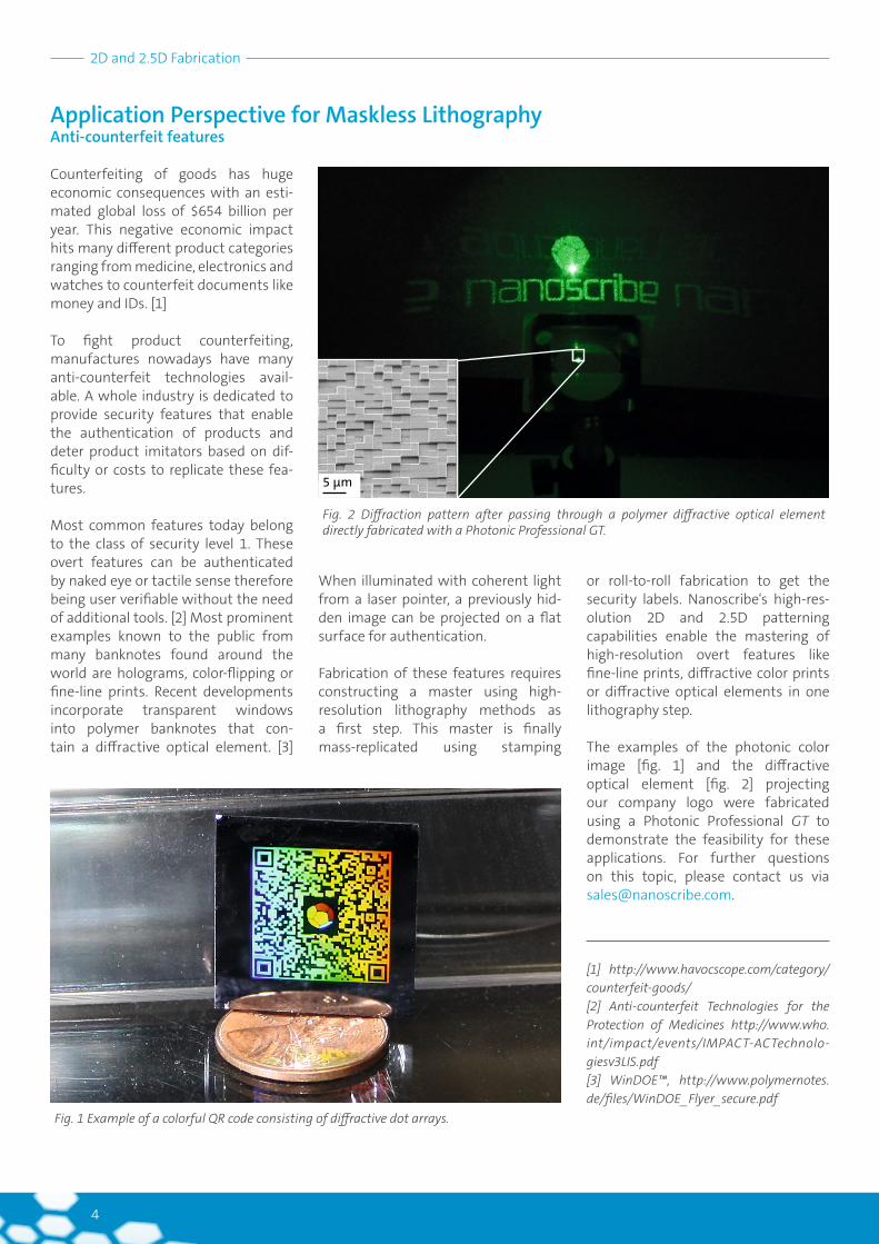
Counterfeiting of goods has huge economic consequences with an esti-mated global loss of $654 billion per year. This negative economic impact hits many different product categories ranging from medicine, electronics and watches to counterfeit documents like money and IDs. [1]
To fight product counterfeiting, manufactures nowadays have many anti-counterfeit technologies avail-able. A whole industry is dedicated to provide security features that enable the authentication of products and deter product imitators based on dif-ficulty or costs to replicate these fea-tures.
Most common features today belong to the class of security level 1. These overt features can be authenticated by naked eye or tactile sense therefore being user verifiable without the need of additional tools. [2] Most prominent examples known to the public from many banknotes found around the world are holograms, color-flipping or fine-line prints. Recent developments incorporate transparent windows into polymer banknotes that con-tain a diffractive optical element. [3]
Fig. 2 Diffraction pattern after passing through a polymer diffractive optical element directly fabricated with a Photonic Professional GT.
When illuminated with coherent light from a laser pointer, a previously hid-den image can be projected on a flat surface for authentication.
Fabrication of these features requires constructing a master using high- resolution lithography methods as a first step. This master is finally mass-replicated using stamping
or roll-to-roll fabrication to get the security labels. Nanoscribe‘s high-res-olution 2D and 2.5D patterning capabilities enable the mastering of high-resolution overt features like fine-line prints, diffractive color prints or diffractive optical elements in one lithography step.
The examples of the photonic color image [fig. 1] and the diffractive optical element [fig. 2] projecting our company logo were fabricated using a Photonic Professional GT to demonstrate the feasibility for these applications. For further questions on this topic, please contact us via [email protected].
[1] http://www.havocscope.com/category/counterfeit-goods/[2] Anti-counterfeit Technologies for the Protection of Medicines http://www.who.int/impact/events/IMPACT-ACTechnolo-giesv3LIS.pdf[3] WinDOE™, http://www.polymernotes.de/files/WinDOE_Flyer_secure.pdf
Fig. 1 Example of a colorful QR code consisting of diffractive dot arrays.
5 µm
2D and 2.5D Fabrication
5
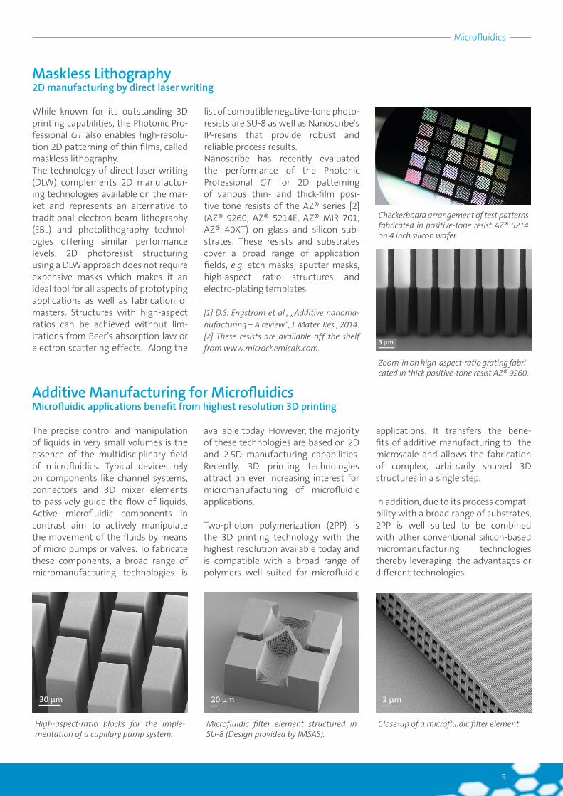
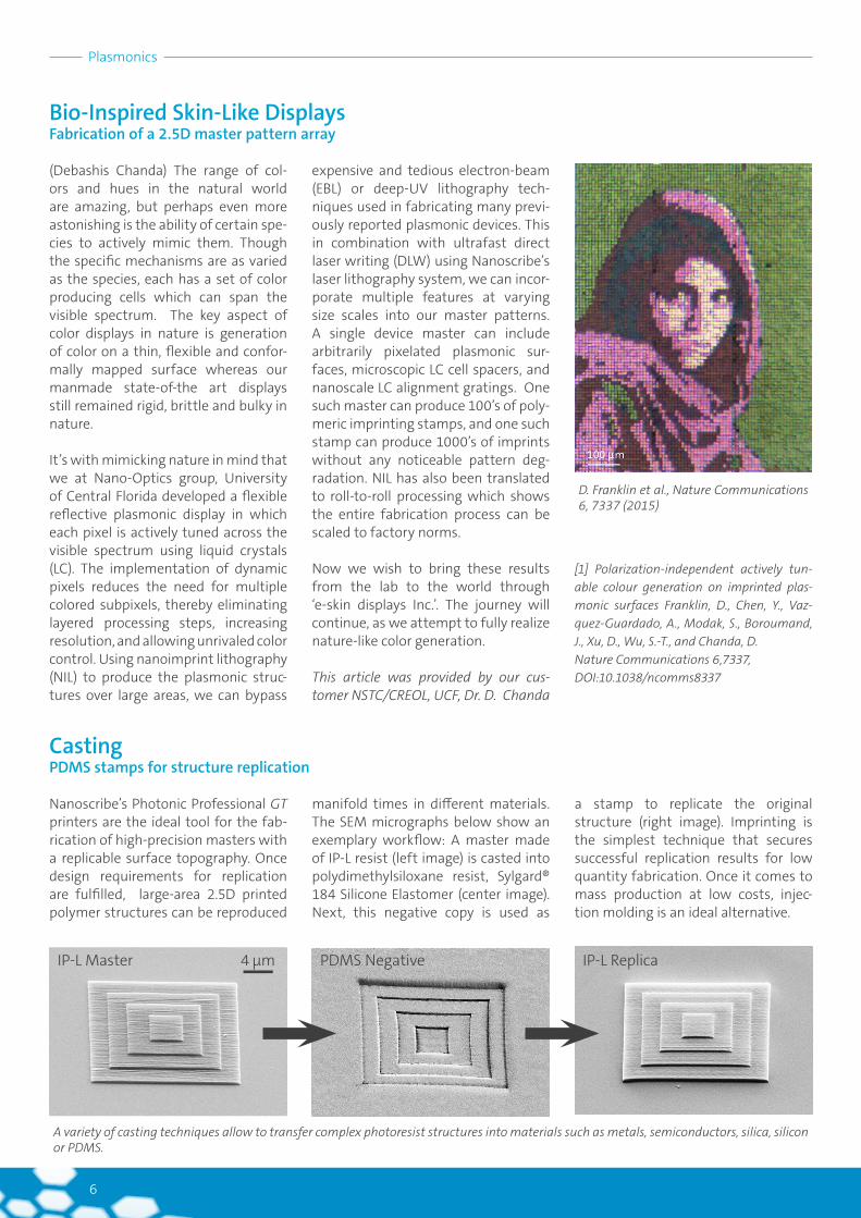
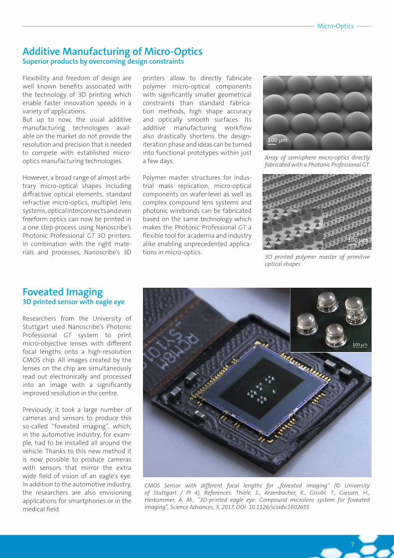
Additive Manufacturing for MicrofluidicsMicrofluidic applications benefit from highest resolution 3D printing
High-aspect-ratio blocks for the imple-mentation of a capillary pump system.
Microfluidic filter element structured in SU-8 (Design provided by IMSAS).
The precise control and manipulation of liquids in very small volumes is the essence of the multidisciplinary field of microfluidics. Typical devices rely on components like channel systems, connectors and 3D mixer elements to passively guide the flow of liquids. Active microfluidic components in contrast aim to actively manipulate the movement of the fluids by means of micro pumps or valves. To fabricate these components, a broad range of micromanufacturing technologies is
available today. However, the majority of these technologies are based on 2D and 2.5D manufacturing capabilities. Recently, 3D printing technologies attract an ever increasing interest for micromanufacturing of microfluidic applications.
Two-photon polymerization (2PP) is the 3D printing technology with the highest resolution available today and is compatible with a broad range of polymers well suited for microfluidic
applications. It transfers the bene-fits of additive manufacturing to the microscale and allows the fabrication of complex, arbitrarily shaped 3D structures in a single step.
In addition, due to its process compati-bility with a broad range of substrates, 2PP is well suited to be combined with other conventional silicon-based micromanufacturing technologies there by leveraging the advantages or different technologies.
20 µm
Close-up of a microfluidic filter element
2 µm
Microfluidics
30 µm
While known for its outstanding 3D printing capabilities, the Photonic Pro-fessional GT also enables high-resolu-tion 2D patterning of thin films, called maskless lithography. The technology of direct laser writing (DLW) complements 2D manufactur-ing technologies available on the mar-ket and represents an alternative to traditional electron-beam litho graphy (EBL) and photolithography technol-ogies offering similar performance levels. 2D photoresist structuring using a DLW approach does not require expensive masks which makes it an ideal tool for all aspects of prototyping applications as well as fabrication of masters. Structures with high-aspect ratios can be achieved without lim-itations from Beer’s absorption law or electron scattering effects. Along the
Maskless Lithography2D manufacturing by direct laser writing
list of compatible negative-tone photo-resists are SU-8 as well as Nanoscribe’s IP-resins that provide robust and reliable process results. Nanoscribe has recently evaluated the performance of the Photonic Professional GT for 2D patterning of various thin- and thick-film posi-tive tone resists of the AZ® series [2] (AZ® 9260, AZ® 5214E, AZ® MIR 701, AZ® 40XT) on glass and silicon sub-strates. These resists and substrates cover a broad range of application fields, e.g. etch masks, sputter masks, high-aspect ratio structures and electro -plating templates.
[1] D.S. Engstrom et al., „Additive nanoma-
nufacturing – A review“, J. Mater. Res., 2014.
[2] These resists are available off the shelf
from www.microchemicals.com.
Checkerboard arrangement of test patterns fabricated in positive-tone resist AZ® 5214 on 4 inch silicon wafer.
Zoom-in on high-aspect-ratio grating fabri-cated in thick positive-tone resist AZ® 9260.
6
Bio-Inspired Skin-Like DisplaysFabrication of a 2.5D master pattern array
(Debashis Chanda) The range of col-ors and hues in the natural world are amazing, but perhaps even more astonishing is the ability of certain spe-cies to actively mimic them. Though the specific mechanisms are as varied as the species, each has a set of color producing cells which can span the visible spectrum. The key aspect of color displays in nature is generation of color on a thin, flexible and confor-mally mapped surface whereas our manmade state-of-the art displays still remained rigid, brittle and bulky in nature.
It’s with mimicking nature in mind that we at Nano-Optics group, University of Central Florida developed a flexible reflective plasmonic display in which each pixel is actively tuned across the visible spectrum using liquid crystals (LC). The implementation of dynamic pixels reduces the need for multiple colored subpixels, thereby eliminating layered processing steps, increasing resolution, and allowing unrivaled color control. Using nanoimprint lithography (NIL) to produce the plasmonic struc-tures over large areas, we can bypass
expensive and tedious electron-beam (EBL) or deep-UV lithography tech-niques used in fabricating many previ-ously reported plasmonic devices. This in combination with ultrafast direct laser writing (DLW) using Nanoscribe’s laser lithography system, we can incor-porate multiple features at varying size scales into our master patterns. A single device master can include arbitrarily pixelated plasmonic sur-faces, microscopic LC cell spacers, and nanoscale LC alignment gratings. One such master can produce 100’s of poly-meric imprinting stamps, and one such stamp can produce 1000’s of imprints without any noticeable pattern deg-radation. NIL has also been translated to roll-to-roll processing which shows the entire fabrication process can be scaled to factory norms.
Now we wish to bring these results from the lab to the world through ‘e-skin displays Inc.’. The journey will continue, as we attempt to fully realize nature-like color generation.
This article was provided by our cus-tomer NSTC/CREOL, UCF, Dr. D. Chanda
D. Franklin et al., Nature Communications 6, 7337 (2015)
[1] Polarization-independent actively tun-
able colour generation on imprinted plas-
monic surfaces Franklin, D., Chen, Y., Vaz-
quez-Guardado, A., Modak, S., Boroumand,
J., Xu, D., Wu, S.-T., and Chanda, D.
Nature Communications 6,7337,
DOI:10.1038/ncomms8337
Nanoscribe’s Photonic Professional GT printers are the ideal tool for the fab-rication of high-precision masters with a replicable surface topography. Once design requirements for replication are fulfilled, large-area 2.5D printed polymer structures can be reproduced
IP-L Master 4 µm PDMS Negative IP-L Replica
manifold times in different materials. The SEM micrographs below show an exemplary workflow: A master made of IP-L resist (left image) is casted into polydimethylsiloxane resist, Sylgard® 184 Silicone Elastomer (center image). Next, this negative copy is used as
a stamp to replicate the original structure (right image). Imprinting is the simplest technique that secures successful replication results for low quantity fabrication. Once it comes to mass production at low costs, injec-tion molding is an ideal alternative.
CastingPDMS stamps for structure replication
A variety of casting techniques allow to transfer complex photoresist structures into materials such as metals, semiconductors, silica, silicon or PDMS.
Plasmonics
7
Micro-Optics
Additive Manufacturing of Micro-OpticsSuperior products by overcoming design constraints
Flexibility and freedom of design are well known benefits associated with the technology of 3D printing which enable faster innovation speeds in a variety of applications.But up to now, the usual additive manufacturing technologies avail-able on the market do not provide the resolution and precision that is needed to compete with established micro- optics manufacturing technologies.
However, a broad range of almost arbi-trary micro-optical shapes including diffractive optical elements, standard refractive micro-optics, multiplet lens systems, optical interconnects and even freeform optics can now be printed in a one step-process using Nanoscribe’s Photonic Professional GT 3D printers. In combination with the right mate-rials and processes, Nanoscribe’s 3D
printers allow to directly fabricate polymer micro-optical components with significantly smaller geometrical constraints than standard fabrica-tion methods, high shape accuracy and optically smooth surfaces. Its additive manufacturing workflow also drastically shortens the design- iteration phase and ideas can be turned into functional prototypes within just a few days.
Polymer master structures for indus-trial mass replication, micro-optical components on wafer-level as well as complex compound lens systems and photonic wirebonds can be fabricated based on the same technology which makes the Photonic Professional GT a flexible tool for academia and industry alike enabling unprecedented applica-tions in micro-optics.
Foveated Imaging3D printed sensor with eagle eye
Researchers from the University of Stuttgart used Nanoscribe’s Photonic Professional GT system to print micro-objective lenses with different focal lengths onto a high-resolution CMOS chip. All images created by the lenses on the chip are simultaneously read out electronically and processed into an image with a significantly improved resolution in the centre.
Previously, it took a large number of cameras and sensors to produce this so-called “foveated imaging”, which, in the automotive industry, for exam-ple, had to be installed all around the vehicle. Thanks to this new method it is now possible to produce cameras with sensors that mirror the extra wide field of vision of an eagle’s eye. In addition to the automotive industry, the researchers are also envisioning applications for smartphones or in the medical field.
CMOS Sensor with different focal lengths for „foveated imaging“ (© University of Stuttgart / PI 4), References: Thiele, S., Arzenbacher, K., Gissibl, T., Giessen, H., Herkommer, A. M., “3D-printed eagle eye: Compound microlens system for foveated imaging”, Science Advances, 3, 2017, DOI: 10.1126/sciadv.1602655
3D printed polymer master of primitive optical shapes
Array of semisphere micro-optics directly fabricated with a Photonic Professional GT.
100 µm
100 µm
8
After the invention of the laser in 1960, optics turned into photonics. In today’s telecommunication tech nology, pho-tons have already become the main carrier of information. During the last decades, a number of pioneering developments such as, e.g.,
3D PhotonicsSemiconductors & metamaterials for light
Above: Bi-chiral photonic crystals, produced by the group of Prof. Dr. Martin Wegener (KIT).
Right: 3D photonic crystalline diamond structure. With permission of Prof. Dr. Keiichi Edagawa, University of Tokyo.
2 µm
Circular spirals seen from above.
1 µm
the concepts of photonic crystals and metamaterials have opened the door to a completely new class of materials.
Molding the flow of light as well as controlling the dynamics of photons are two key issues. The properties of
Photonics
20 µm
such nanostructured materials are subject of current research activities.
Shown is a series of structures fabri-cated by means of the direct laser writ-ing process achieved with Photonic Professional GT systems.
[1] V. Miikkulainen et al., J. Appl. Phys. 113, 021301 (2013); [2] M. Hermatschweiler et al., Adv. Funct. Mater. 17, 2273 (2007)[3] A. Radke et al., Adv. Mater. 23, 3018 (2011); [4] J. Gansel et al., Science 325, 1513 (2009)
Polymer Gold
With two-photon polymerization 3D microprinting almost arbitrarily shaped polymer nano- and microstructures can be made. Replicating, inverting or coat-ing a printed structure in/with a mate-rial of choice, allows for nearly limitless
Coating and Plating Processes for Polymer TemplatesTurning 3D printed polymer microstructures into other materials
freedom of design and functionality. Electro- and electroless plating, chem-ical vapor deposition (CVD) and atomic layer deposition (ALD) are deposition techniques that can be used to deposit material in 3D microtemplates: ALD [1],
CVD [2], and electroless plating [3] deposit material on all surfaces of an object. Electroplating [4] is used to grow metals into the tubes of 3D tem-plates, starting from the conductive substrate surface, as shown below.

9
(Nicole Lindenmann) The demand for ever higher data rates poses an increas-ing challenge for electrical intercon-nects. Fundamental limita tions such as size, speed and crosstalk call for a radically new approach, especially with regard to inter chip connections.
In this context, optical interconnects are considered a promising candi-date to overcome communication bottlenecks in data centers and high- performance computers. However, while tremendous progress has been made in integrating optical transmit-ters and receivers on semiconductor chips, there is currently no technology at hand that can cope with these chal-lenges beyond chip edges. A group of researchers led by Prof. Christian Koos from Karls ruhe Institute
Photonic Wire BondsA novel concept for chip-to-chip interconnects
of Technology (KIT), Germany, has now demonstrated a photonic chip-to-chip interconnect, a Photonic Wire Bond (PWB), as they named it (1). This con-cept is illustrated in figure (a). Taking advantage of live imaging and three-dimensional writing capa-bility of the Photonic Professional, silicon- on-insulator waveguides on separate chips are connected by a freeform polymer PWB, figure (b). The structure is formed by tightly focused femtosecond laser pulses that expose the photoresist precisely along the computed trajectory. The shape of the wire bond is adapted to the position and orientation of the chips, rendering high-precision mechanical alignment unnecessary and bringing industrial scale application of PWBs into reach, see figure (c).
All pictures: Courtesy of Prof. Christian Koos, Karlsruhe Institute of Technology (KIT/IPQ), Germany Reference (1): N. Lindenmann, G. Balthasar, D. Hillerkuss, R. Schmogrow, M. Jordan, J. Leuthold, W. Freude, and C. Koos, “Photonic wire bonding: a novel concept for chip-scale interconnects,” Opt. Express 20, 17667-17677 (2012).
Top view of multiple PWBFigure (c)
SOI waveguides
Chip 1
Photonic Wire Bond
Chip 2
Figure (b)
Proof-of-principle devices exhibit low losses at infrared telecommuni-cation wavelengths around 1.55 µm and permit transmission of data rates exceeding 5 Tbit/s. This technological approach is considered a breakthrough in optical interconnects.
R&D activities with the group of Prof. Christian Koos at KIT, with IBM and Alcatel-Lucent (among others) have been government-funded (BMBF) within the project “Phoibos”. Please consult Nanoscribe for dedicated pho-tonic wire bonders for R&D as well as for large series production in industry.
Photonic Wire Bonds
Figure (a)
10
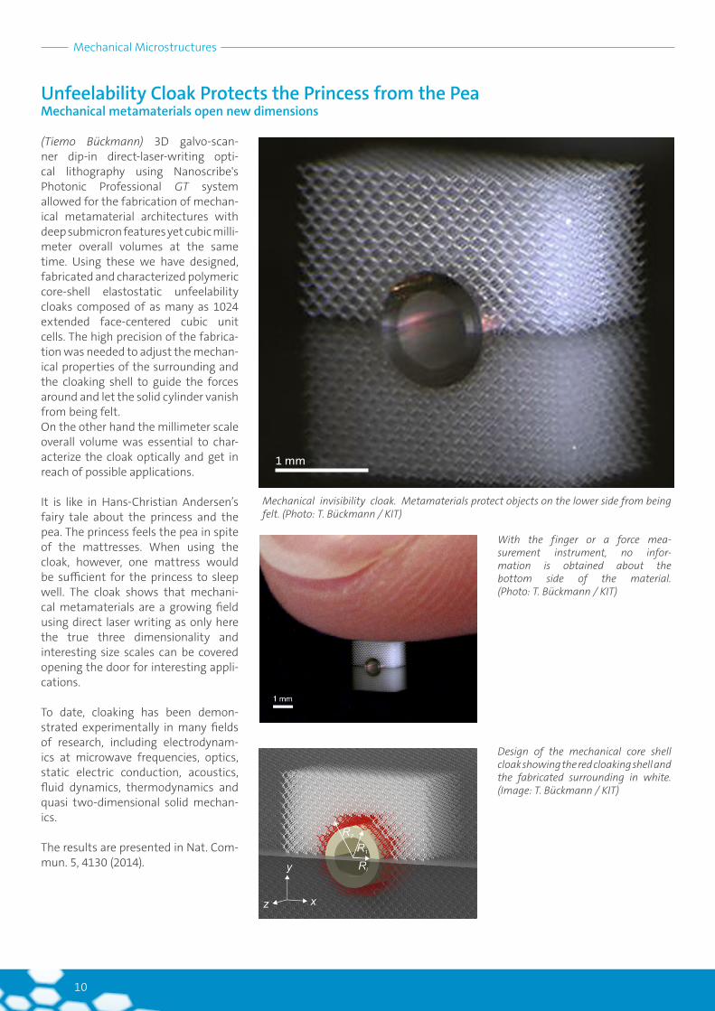
(Tiemo Bückmann) 3D galvo-scan-ner dip-in direct-laser-writing opti-cal lithography using Nanoscribe's Photonic Professional GT system allowed for the fabrication of mechan-ical metamaterial architectures with deep submicron features yet cubic milli- meter overall volumes at the same time. Using these we have designed, fabricated and characterized polymeric core-shell elastostatic unfeelability cloaks composed of as many as 1024 extended face-centered cubic unit cells. The high precision of the fabrica-tion was needed to adjust the mechan-ical properties of the surrounding and the cloaking shell to guide the forces around and let the solid cylinder vanish from being felt. On the other hand the millimeter scale overall volume was essential to char-acterize the cloak optically and get in reach of possible applications.
It is like in Hans-Christian Andersen’s fairy tale about the princess and the pea. The princess feels the pea in spite of the mattresses. When using the cloak, however, one mattress would be sufficient for the princess to sleep well. The cloak shows that mechani-cal metamaterials are a growing field using direct laser writing as only here the true three dimensionality and interesting size scales can be covered opening the door for interesting appli-cations.
To date, cloaking has been demon-strated experimentally in many fields of research, including electrodynam-ics at microwave frequencies, optics, static electric conduction, acoustics, fluid dynamics, thermodynamics and quasi two-dimensional solid mechan-ics.
The results are presented in Nat. Com-mun. 5, 4130 (2014).
Unfeelability Cloak Protects the Princess from the PeaMechanical metamaterials open new dimensions
With the finger or a force mea-surement instrument, no infor- mation is obtained about the bottom side of the material. (Photo: T. Bückmann / KIT)
Mechanical invisibility cloak. Metamaterials protect objects on the lower side from being felt. (Photo: T. Bückmann / KIT)
Mechanical Microstructures
Design of the mechanical core shell cloak showing the red cloaking shell and the fabricated surrounding in white. (Image: T. Bückmann / KIT)
1 mm
11
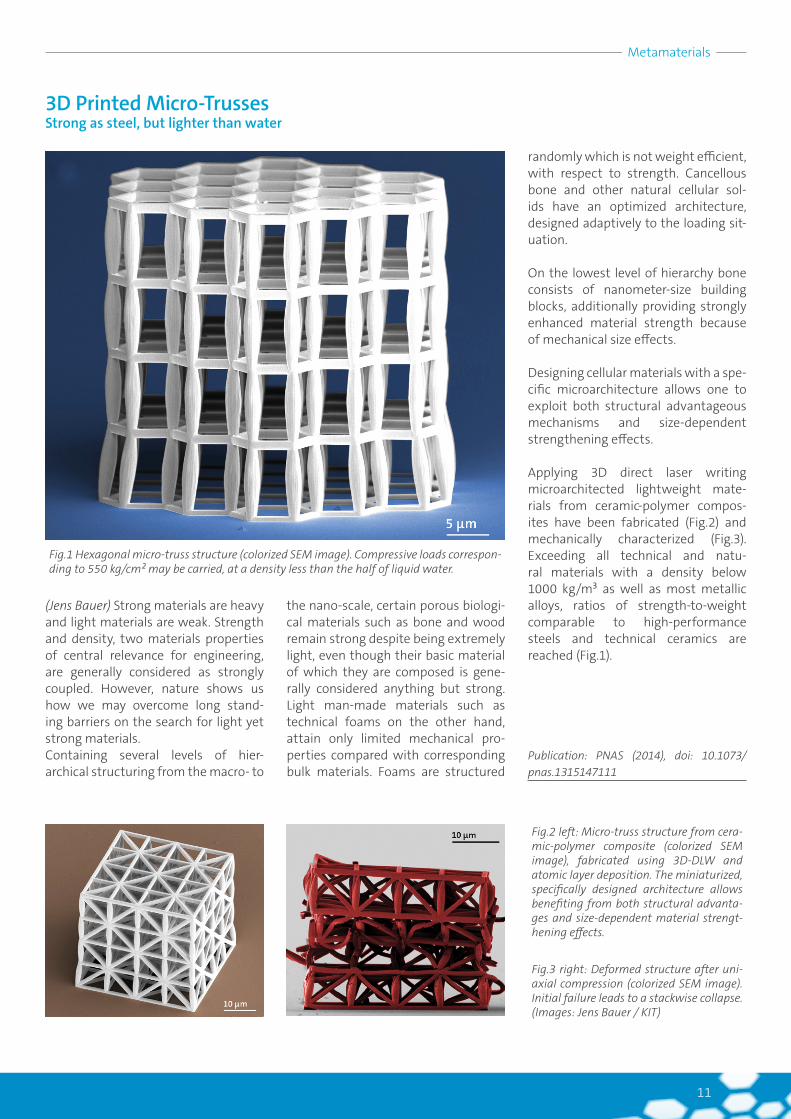
3D Printed Micro-TrussesStrong as steel, but lighter than water
(Jens Bauer) Strong materials are heavy and light materials are weak. Strength and density, two materials properties of central relevance for engineering, are generally considered as strongly coupled. However, nature shows us how we may overcome long stand-ing barriers on the search for light yet strong materials. Containing several levels of hier-archical structuring from the macro- to
Fig.1 Hexagonal micro-truss structure (colorized SEM image). Compressive loads correspon-ding to 550 kg/cm² may be carried, at a density less than the half of liquid water.
the nano-scale, certain porous biologi- cal materials such as bone and wood remain strong despite being extremely light, even though their basic material of which they are composed is gene-rally considered anything but strong. Light man-made materials such as technical foams on the other hand, attain only limited mechanical pro-perties compared with corresponding bulk materials. Foams are structured
randomly which is not weight efficient, with respect to strength. Cancellous bone and other natural cellular sol-ids have an optimized architecture, designed adaptively to the loading sit-uation.
On the lowest level of hierarchy bone consists of nanometer-size building blocks, additionally providing strongly enhanced material strength because of mechanical size effects.
Designing cellular materials with a spe-cific microarchitecture allows one to exploit both structural advantageous mechanisms and size-dependent strengthening effects.
Applying 3D direct laser writing micro architected lightweight mate-rials from ceramic- polymer compos-ites have been fabricated (Fig.2) and mechanically characterized (Fig.3). Exceeding all technical and natu-ral materials with a density below 1000 kg/m³ as well as most metallic alloys, ratios of strength-to-weight comparable to high-performance steels and technical ceramics are reached (Fig.1).
Publication: PNAS (2014), doi: 10.1073/pnas.1315147111
Fig.3 right: Deformed structure after uni-axial compression (colorized SEM image). Initial failure leads to a stackwise collapse.(Images: Jens Bauer / KIT)
Fig.2 left: Micro-truss structure from cera-mic-polymer composite ( colorized SEM image), fabricated using 3D-DLW and atomic layer deposition. The miniaturized, specifically designed architecture allows benefiting from both structural advanta-ges and size-dependent material strengt-hening effects.
Metamaterials
12
In the last decades cells have been intensively studied by biologists in artificially structured two-dimen-sional environments. In order to shine even more light onto their behavior in a rather natural environment 3D scaffolds were created by means of Nanoscribe’s 3D printers.
In one of Nanoscribe's newsletters chicken heart cells beating in a 3D scaffold were presented as an achieve-ment of the group of Prof. Martin Bastmeyer at the Karlsruhe Institute of
Technology (KIT), Germany, revealing the force of individual cells exerted in a 3D topology.
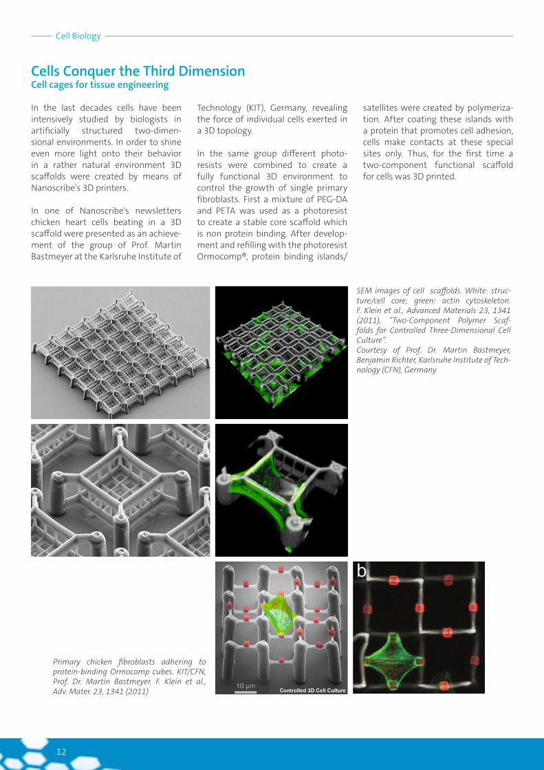
In the same group different photo-resists were combined to create a fully functional 3D environment to control the growth of single primary fibroblasts. First a mixture of PEG-DA and PETA was used as a photoresist to create a stable core scaffold which is non protein binding. After develop-ment and refilling with the photoresist Ormocomp®, protein binding islands/
SEM images of cell scaffolds. White: struc-ture/cell core; green: actin cytoskeleton. F. Klein et al., Advanced Materials 23, 1341 (2011), “Two-Component Polymer Scaf-folds for Controlled Three- Dimensional Cell Culture”.Courtesy of Prof. Dr. Martin Bastmeyer, Benjamin Richter, Karlsruhe Institute of Tech-nology (CFN), Germany
Cells Conquer the Third Dimension Cell cages for tissue engineering
satellites were created by polymeriza-tion. After coating these islands with a protein that promotes cell adhesion, cells make contacts at these special sites only. Thus, for the first time a two-component functional scaffold for cells was 3D printed.
Primary chicken fibroblasts adhering to protein-binding Ormocomp cubes. KIT/CFN, Prof. Dr. Martin Bastmeyer, F. Klein et al., Adv. Mater. 23, 1341 (2011)
Cell Biology
13
Tissue Engineering
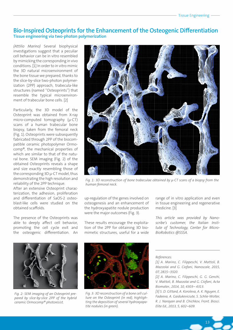
(Attilio Marino) Several biophysical investigations suggest that a peculiar cell behavior can be in vitro resembled by mimicking the corresponding in vivo conditions. [1] In order to in vitro mimic the 3D natural microenvironment of the bone tissue we prepared, thanks to the slice-by-slice two-photon polymer-ization (2PP) approach, trabecula-like structures (named ‘‘Osteoprints’’) that resemble the typical microenviron-ment of trabecular bone cells. [2]
Particularly, the 3D model of the Osteoprint was obtained from X-ray micro-computed tomography (µ-CT) scans of a human trabecular bone biopsy, taken from the femoral neck (Fig. 1). Osteoprints were subsequently fabricated through 2PP of the biocom-patible ceramic photopolymer Ormo-comp®, the mechanical properties of which are similar to that of the natu-ral bone. SEM imaging (Fig. 2) of the obtained Osteoprints reveals a shape and size exactly resembling those of the corresponding 3D µ-CT model, thus demonstrating the high resolution and reliability of the 2PP technique. After an extensive Osteoprint charac-terization, the adhesion, proliferation and differentiation of SaOS-2 osteo-blast-like cells were studied on the obtained scaffolds.
The presence of the Osteoprints was able to deeply affect cell behavior, promoting the cell cycle exit and the osteogenic differentiation. An
Bio-Inspired Osteoprints for the Enhancement of the Osteogenic DifferentiationTissue engineering via two-photon polymerization
Fig. 2: SEM imaging of an Osteoprint pre-pared by slice-by-slice 2PP of the hybrid ceramic Ormocomp® photoresist.
Fig. 1: 3D reconstruction of bone trabeculae obtained by µ-CT scans of a biopsy from the human femoral neck.
Fig. 3: 3D reconstruction of a bone cell cul-ture on the Osteoprint (in red), highligh-ting the deposition of several hydroxyapa-tite nodules (in green).
up-regulation of the genes involved on osteogenesis and an enhancement of the hydroxyapatite nodule production were the major outcomes (Fig. 3).
These results encourage the exploita-tion of the 2PP for obtaining 3D bio-mimetic structures, useful for a wide
range of in vitro application and even in tissue engineering and regenerative medicine. [3]
This article was provided by Nano-scribe’s customer, the Italian Insti-tute of Technology, Center for Micro- BioRobotics @SSSA.
References:[1] A. Marino, C. Filippeschi, V. Mattoli, B. Mazzolai and G. Ciofani, Nanoscale, 2015, 07, 2815–3320.[2] A. Marino, C. Filippeschi, G. G. Genchi, V. Mattoli, B. Mazzolai and G. Ciofani, Acta Biomater., 2014, 10, 4303– 4313.[3] S. D. Gittard, A. Koroleva, A. K. Nguyen, E. Fadeeva, A. Gaidukeviciute, S. Schlie-Wolter, R. J. Narayan and B. Chichkov, Front. Biosci. Elite Ed., 2013, 5, 602–609.
14
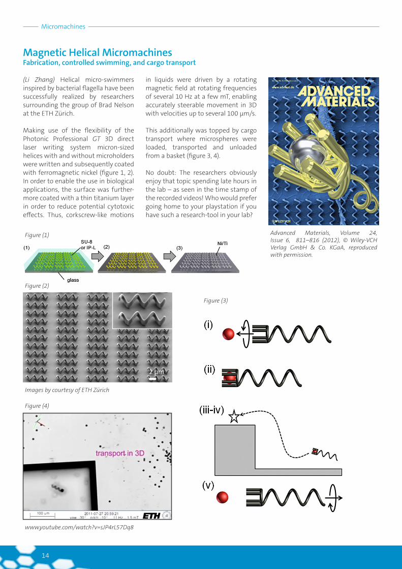
(Li Zhang) Helical micro-swimmers inspired by bacterial flagella have been successfully realized by researchers surrounding the group of Brad Nelson at the ETH Zürich.
Making use of the flexibility of the Photonic Professional GT 3D direct laser writing system micron-sized helices with and without microholders were written and subsequently coated with ferromagnetic nickel (figure 1, 2). In order to enable the use in biological applications, the surface was further-more coated with a thin titanium layer in order to reduce potential cytotoxic effects. Thus, corkscrew-like motions
Magnetic Helical Micromachines Fabrication, controlled swimming, and cargo transport
in liquids were driven by a rotating magnetic field at rotating frequencies of several 10 Hz at a few mT, enabling accurately steerable movement in 3D with velocities up to several 100 µm/s.
This additionally was topped by cargo transport where microspheres were loaded, transported and unloaded from a basket (figure 3, 4).
No doubt: The researchers obviously enjoy that topic spending late hours in the lab – as seen in the time stamp of the recorded videos! Who would prefer going home to your playstation if you have such a research-tool in your lab?
Advanced Materials, Volume 24, Issue 6, 811–816 (2012), © Wiley-VCH Verlag GmbH & Co. KGaA, reproduced with permission.
Figure (1)
Figure (3)
Images by courtesy of ETH Zürich
2 µm
Figure (2)
www.youtube.com/watch?v=sJP4rL57Dq8
Figure (4)
Micromachines
15
Micro Rapid Prototyping
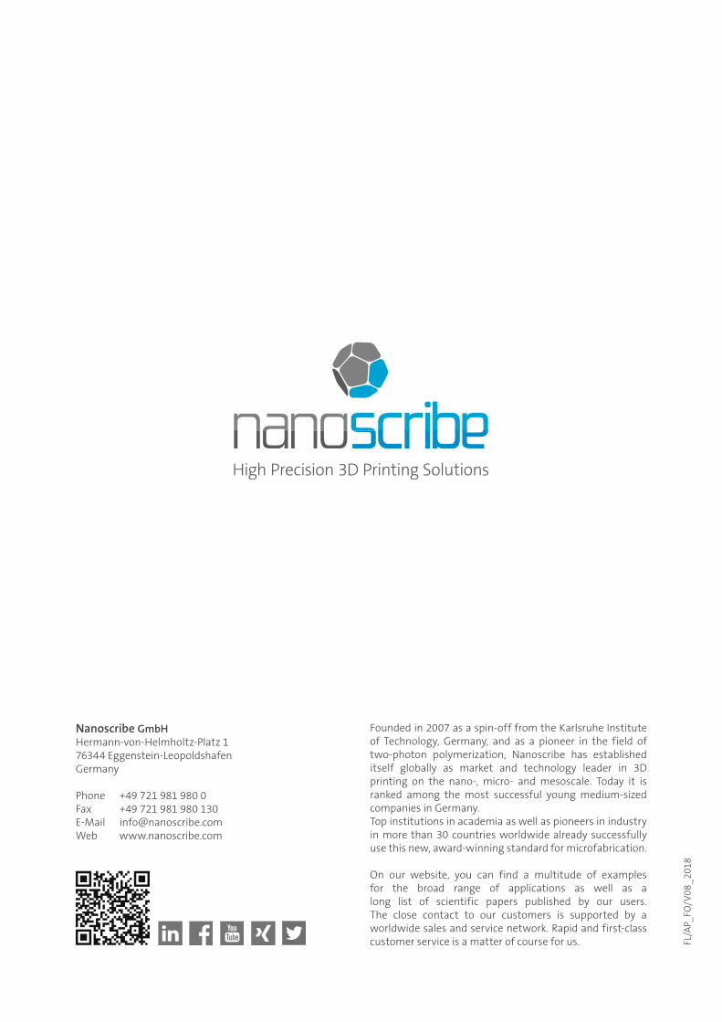
Following the trend of miniaturization 3D printing on the microscale needs to provide excellent resolution to allow for the fabrication of finest features.Micro-sized parts have a great poten-tial in a wide variety of applications like optics, photonics, biotechnology, life-sciences, micro fluidics and many more. For applications where compo-nents and devices with feature-sizes on the micro/meso-scale (10² - 104 µm) are needed, additive manufacturing based on two-photon polymerization provides the necessary resolution to transfer the benefits of 3D printing to this scale. Among these advantages are cost-effective production of complex structures and functional integration for low volume production down to a lot size of one.
In a recent publication of Optics Express*, researchers from the Arizona State University demonstrated the ben-efits of highest-resolution 3D printing for the fabrication of complex shaped nozzles that are directly used for their experimental work. For biological imag-ing using X-ray Free Electron Lasers, the use of gas dynamic virtual nozzles has proven to be valuable method for reliable sample delivery. However, the standard method of fabricating these nozzles manually represents a cumbersome and error prone process. The researchers successfully used a Photonic Professional GT to consoli-date several manual fabrication steps into one single automatic 3D printing step. The high-resolution 3D printing of polymer micro nozzles from CAD data enables the researchers to not only gain flexibility for design iterations but also to reduce the quality variances inherent in the standard manual fab-rication method. As demonstrated by testing the jetting behavior, these nozzles provide high quality per-formance and have the potential to become the new standard in this field of research.Further examples of mesoscopic struc-tures are demonstrated in the image gallery on the right side.
Rapid Prototyping of Micro- and Mesoparts Two-photon polymerization transfers the benefits of 3D printing to the microscale.
3D printed micro connectors.
Mechanical mixer structure with filigree mixer blades.
1 mm
Porous lattice tower.
Rendering of the STL with a cut-out to show the inner complexity of the nozzle design (left) and the final 3D print from the STL (right). *Optics Express, Vol 24, Issue 11, pp. 11515 (2016)
1 mm
100 µm 100 µm
1 mm
Nanoscribe GmbHHermann-von-Helmholtz-Platz 176344 Eggenstein-LeopoldshafenGermany
Phone +49 721 981 980 0Fax +49 721 981 980 130E-Mail [email protected] www.nanoscribe.com
FL/A
P_FO
/V08
_20
18
Founded in 2007 as a spin-off from the Karlsruhe Institute of Technology, Germany, and as a pioneer in the field of two-photon polymerization, Nanoscribe has established itself globally as market and technology leader in 3D printing on the nano-, micro- and mesoscale. Today it is ranked among the most successful young medium-sized companies in Germany. Top institutions in academia as well as pioneers in industry in more than 30 countries worldwide already successfully use this new, award-winning standard for microfabrication.
On our website, you can find a multitude of examples for the broad range of applications as well as a long list of scientific papers published by our users. The close contact to our customers is supported by a worldwide sales and service network. Rapid and first-class customer service is a matter of course for us.