Spectrum Analyzer Fundamentals - rohde-schwarz … Analyzer Fundamentals – Theory ... 32 3...
65
Spectrum Analyzer Fundamentals – Theory and Operation of Modern Spectrum Analyzers Primer This primer examines the theory of state-of-the-art spectrum analysis and describes how modern spectrum analyzers are designed and how they work. That is followed by a brief characterization of today's signal generators, which are needed as a stimulus when performing amplifier measurements. Detlev Libel 003.008.029.13 Primer
Transcript of Spectrum Analyzer Fundamentals - rohde-schwarz … Analyzer Fundamentals – Theory ... 32 3...
Spectrum Analyzer Fundamentals – Theory and Operation of Modern Spectrum Analyzers Primer
This primer examines the theory
of state-of-the-art spectrum analysis
and describes how modern spectrum
analyzers are designed and how they
work. That is followed by a brief
characterization of today's signal
generators, which are needed as a
stimulus when performing amplifier
measurements.
Det
lev
Libe
l
003.
008.
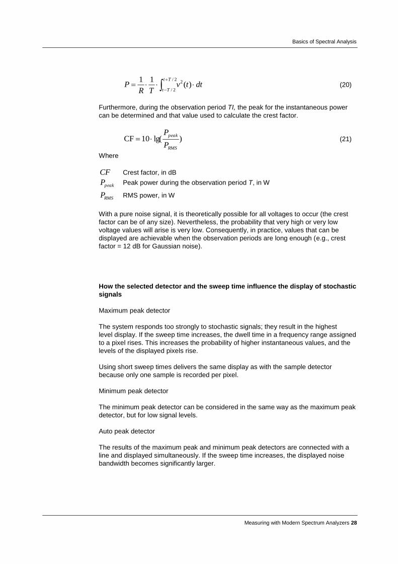
029.
13
Prim
er

Overview
Measuring with Modern Spectrum Analyzers 2
Contents
1 Overview ..................................................................................3
2 Basics of Spectral Analysis ...................................................4
2.1 Correlation between the Time and Frequency Domains .......................... 4
2.2 Fast Fourier Transform (FFT) Analyzers .................................................... 7
2.2.1 Architecture .................................................................................................. 7
2.2.2 How an FFT Analyzer Works ....................................................................... 7
2.2.3 Difference between FFT Analyzers and Oscilloscopes .......................... 10
2.3 Analyzers that Use the Heterodyne Principle.......................................... 11
2.3.1 Architecture ................................................................................................ 11
2.3.2 Frequency Selection .................................................................................. 13
2.3.3 Step-by-Step Tuning of the Local Oscillator (LO) ................................... 17
2.3.4 Intermediate Frequency (IF) Signal Processing ...................................... 18
2.3.5 Envelope Detection and Video Filter ........................................................ 22
2.3.6 Detectors ..................................................................................................... 25
2.4 Combining Both Implementation Approaches ........................................ 30
2.5 Important Terms and Settings .................................................................. 32
3 Generators and Their Use .................................................... 34
3.1 Analog Signal Generators ......................................................................... 34
3.2 Vector Signal Generators .......................................................................... 35
3.3 Arbitrary Waveform Generators (AWGs) ................................................. 39
4 Nonlinearities of the Device under Test (DUT) ................... 42
4.1 1 dB Compression Point............................................................................ 42
4.2 Mathematic Description of Small-Signal Nonlinearities ......................... 43
4.3 Intercept Points IP2 and IP3 ...................................................................... 49
5 Crest Factor and Complementary Cumulative Distribution Function (CCDF) .................................................................... 53
6 Phase Noise ........................................................................... 57
7 Mixers ..................................................................................... 60
8 References ............................................................................. 64
Overview
Measuring with Modern Spectrum Analyzers 3
1 Overview
This primer is divided into eight chapters. Chapter 2 examines the theory of state-of-
the-art spectrum analysis and describes how modern spectrum analyzers are designed
and how they work. That discussion is followed in Chapter 3 by a brief characterization
of today's signal generators, which are required as a stimulus when performing
amplifier measurements. Chapter 4 concludes the theoretical part by showing how the
effects on the spectrum that are caused by the nonlinearity of real devices under test
are derived mathematically. Chapter 5 discusses measurements on signals with a high
crest factor, and Chapter 6 explains phase noise measurements. Chapter 7 concludes
the primer by looking into mixers and mixer measurements.
Basics of Spectral Analysis
Measuring with Modern Spectrum Analyzers 4
2 Basics of Spectral Analysis For the most part, the structure and content of this chapter have been taken from the
book Fundamentals of Spectrum Analysis by Christoph Rauscher [1]. That work
contains further references and links for a more in-depth look at this subject.
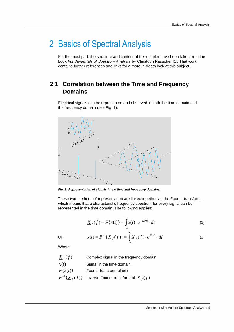
2.1 Correlation between the Time and Frequency
Domains
Electrical signals can be represented and observed in both the time domain and
the frequency domain (see Fig. 1).
Fig. 1: Representation of signals in the time and frequency domains.
These two methods of representation are linked together via the Fourier transform,
which means that a characteristic frequency spectrum for every signal can be
represented in the time domain. The following applies:
dtetxtxFfX ftjf
2)()}({)( (1)
Or:
dfefXfXFtx ftjff
21 )()}({)( (2)
Where
)( fX f Complex signal in the frequency domain
)(tx Signal in the time domain
)}({ txF Fourier transform of x(t)
)}({1 fXF f
Inverse Fourier transform of )( fX f
Basics of Spectral Analysis
Measuring with Modern Spectrum Analyzers 5
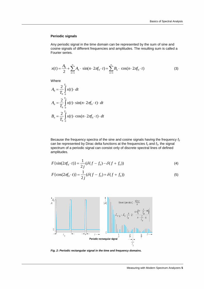
Periodic signals
Any periodic signal in the time domain can be represented by the sum of sine and
cosine signals of different frequencies and amplitudes. The resulting sum is called a
Fourier series.
)2cos()2sin(2
)( 0
1
0
1
0 tfnBtfnAA
txn
n
n
n
(3)
Where
0
00
0 )(2
T
dttxT
A
0
0
0
0
)2sin()(2
T
n dttfntxT
A
0
0
0
0
)2cos()(2
T
n dttfntxT
B
Because the frequency spectra of the sine and cosine signals having the frequency f0
can be represented by Dirac delta functions at the frequencies f0 and f0, the signal
spectrum of a periodic signal can consist only of discrete spectral lines of defined
amplitudes.
))()((2
1)}2{sin( 000 ffff
jtfF (4)
))()((2
1)}2{cos( 000 ffff
jtfF (5)
Fig. 2: Periodic rectangular signal in the time and frequency domains.
Basics of Spectral Analysis
Measuring with Modern Spectrum Analyzers 6
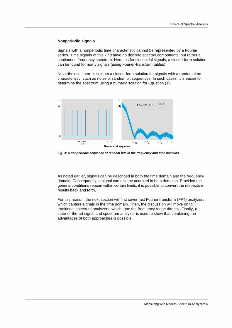
Nonperiodic signals
Signals with a nonperiodic time characteristic cannot be represented by a Fourier
series. Time signals of this kind have no discrete spectral components, but rather a
continuous frequency spectrum. Here, as for sinusoidal signals, a closed-form solution
can be found for many signals (using Fourier-transform tables).
Nevertheless, there is seldom a closed-form solution for signals with a random time
characteristic, such as noise or random bit sequences. In such cases, it is easier to
determine the spectrum using a numeric solution for Equation (1).
Fig. 3: A nonperiodic sequence of random bits in the frequency and time domains.
As noted earlier, signals can be described in both the time domain and the frequency
domain. Consequently, a signal can also be acquired in both domains. Provided the
general conditions remain within certain limits, it is possible to convert the respective
results back and forth.
For this reason, the next section will first cover fast Fourier transform (FFT) analyzers,
which capture signals in the time domain. Then, the discussion will move on to
traditional spectrum analyzers, which tune the frequency range directly. Finally, a
state-of-the-art signal and spectrum analyzer is used to show that combining the
advantages of both approaches is possible.
Basics of Spectral Analysis
Measuring with Modern Spectrum Analyzers 7
2.2 Fast Fourier Transform (FFT) Analyzers
An FFT analyzer calculates the frequency spectrum from a
signal captured in the time domain. Nevertheless, performing an exact
calculation would require an observation period of infinite length. Furthermore,
achieving an exact result for Equation (1) on page 4 would require knowledge of the
signal amplitude at every point in time. The result of that calculation would be a
continuous spectrum, meaning that the frequency resolution would be unlimited.
Obviously, performing such calculations in practice is impossible. Nonetheless, under
certain circumstances, the signal spectrum can be determined with sufficient accuracy.
2.2.1 Architecture
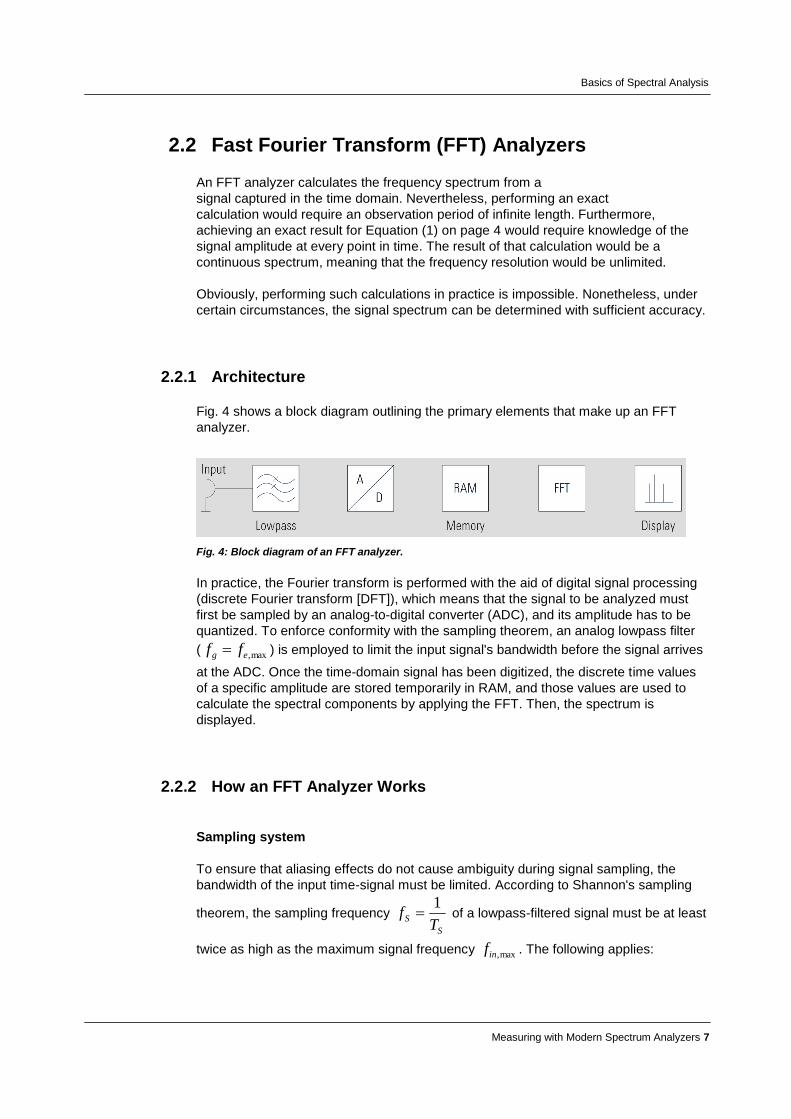
Fig. 4 shows a block diagram outlining the primary elements that make up an FFT
analyzer.
Fig. 4: Block diagram of an FFT analyzer.
In practice, the Fourier transform is performed with the aid of digital signal processing
(discrete Fourier transform [DFT]), which means that the signal to be analyzed must
first be sampled by an analog-to-digital converter (ADC), and its amplitude has to be
quantized. To enforce conformity with the sampling theorem, an analog lowpass filter
( max,eg ff ) is employed to limit the input signal's bandwidth before the signal arrives
at the ADC. Once the time-domain signal has been digitized, the discrete time values
of a specific amplitude are stored temporarily in RAM, and those values are used to
calculate the spectral components by applying the FFT. Then, the spectrum is
displayed.
2.2.2 How an FFT Analyzer Works
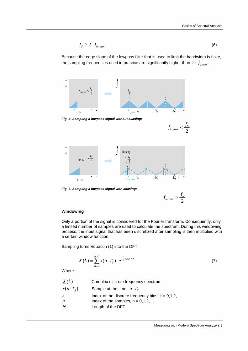
Sampling system
To ensure that aliasing effects do not cause ambiguity during signal sampling, the
bandwidth of the input time-signal must be limited. According to Shannon's sampling
theorem, the sampling frequency
S
ST
f1
of a lowpass-filtered signal must be at least
twice as high as the maximum signal frequency max,inf . The following applies:
Basics of Spectral Analysis
Measuring with Modern Spectrum Analyzers 8
max,2 inS ff
(6)
Because the edge slope of the lowpass filter that is used to limit the bandwidth is finite,
the sampling frequencies used in practice are significantly higher than max,2 ef .
Fig. 5: Sampling a lowpass signal without aliasing:
2
max,S
in
ff
Fig. 6: Sampling a lowpass signal with aliasing:
2max,
Sin
ff
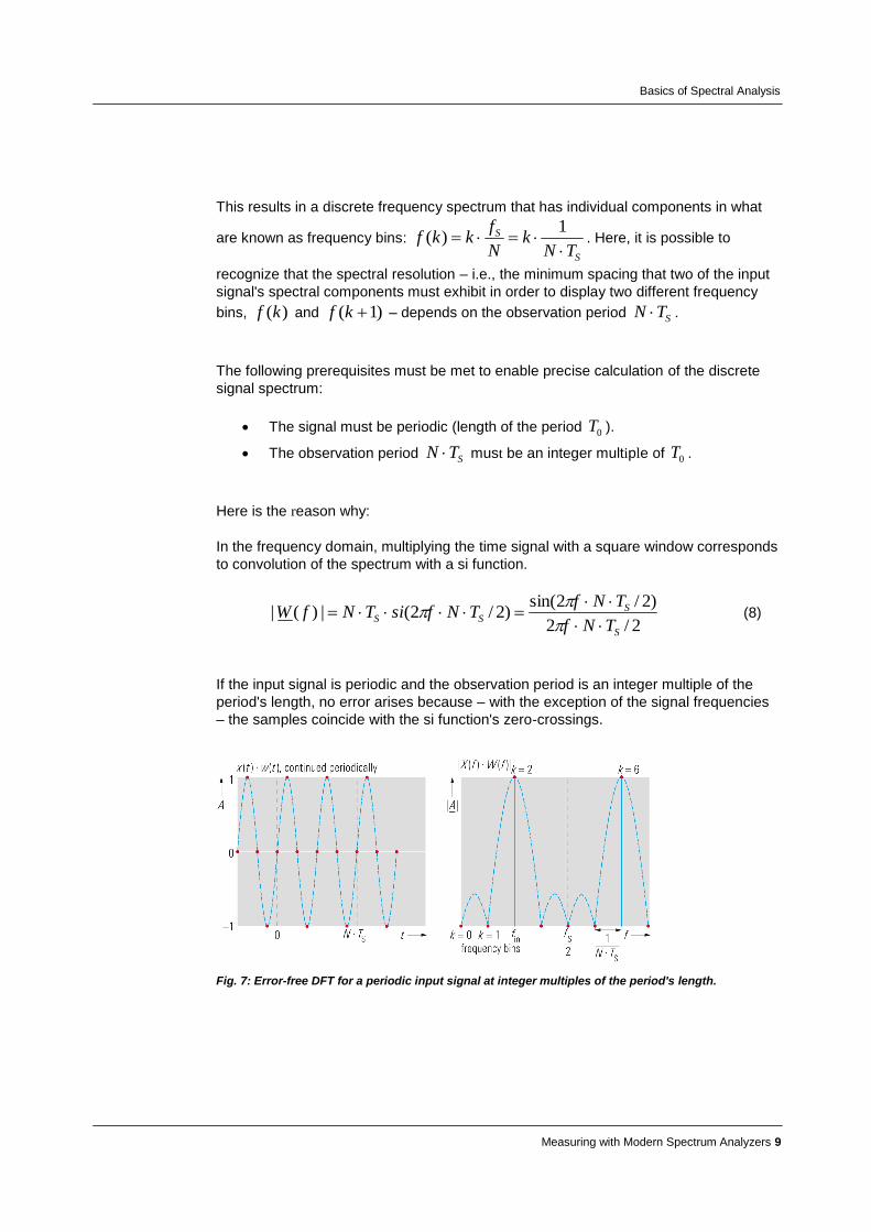
Windowing
Only a portion of the signal is considered for the Fourier transform. Consequently, only
a limited number of samples are used to calculate the spectrum. During this windowing
process, the input signal that has been discretized after sampling is then multiplied with
a certain window function.
Sampling turns Equation (1) into the DFT:
Nknj
N
n
S eTnxkX /21
0
)()(
(7)
Where
)(kX Complex discrete frequency spectrum
)( STnx Sample at the time STn
k Index of the discrete frequency bins, k = 0,1,2,…
n Index of the samples, n = 0,1,2,…
N Length of the DFT
Basics of Spectral Analysis
Measuring with Modern Spectrum Analyzers 9
This results in a discrete frequency spectrum that has individual components in what
are known as frequency bins:
S
S
TNk
N
fkkf
1)( . Here, it is possible to
recognize that the spectral resolution – i.e., the minimum spacing that two of the input
signal's spectral components must exhibit in order to display two different frequency
bins, )(kf and )1( kf – depends on the observation period STN .
The following prerequisites must be met to enable precise calculation of the discrete
signal spectrum:
The signal must be periodic (length of the period 0T ).
The observation period STN must be an integer multiple of 0T .
Here is the reason why:
In the frequency domain, multiplying the time signal with a square window corresponds
to convolution of the spectrum with a si function.
2/2
)2/2sin()2/2(|)(|
S
SSS
TNf
TNfTNfsiTNfW
(8)
If the input signal is periodic and the observation period is an integer multiple of the
period's length, no error arises because – with the exception of the signal frequencies
– the samples coincide with the si function's zero-crossings.
Fig. 7: Error-free DFT for a periodic input signal at integer multiples of the period's length.
Basics of Spectral Analysis
Measuring with Modern Spectrum Analyzers 10
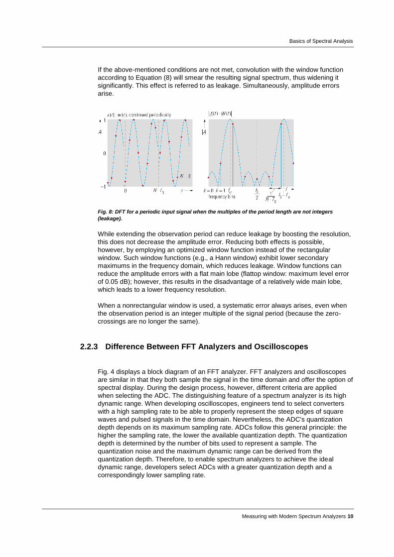
If the above-mentioned conditions are not met, convolution with the window function
according to Equation (8) will smear the resulting signal spectrum, thus widening it
significantly. This effect is referred to as leakage. Simultaneously, amplitude errors
arise.
Fig. 8: DFT for a periodic input signal when the multiples of the period length are not integers
(leakage).
While extending the observation period can reduce leakage by boosting the resolution,
this does not decrease the amplitude error. Reducing both effects is possible,
however, by employing an optimized window function instead of the rectangular
window. Such window functions (e.g., a Hann window) exhibit lower secondary
maximums in the frequency domain, which reduces leakage. Window functions can
reduce the amplitude errors with a flat main lobe (flattop window: maximum level error
of 0.05 dB); however, this results in the disadvantage of a relatively wide main lobe,
which leads to a lower frequency resolution.
When a nonrectangular window is used, a systematic error always arises, even when
the observation period is an integer multiple of the signal period (because the zero-
crossings are no longer the same).
2.2.3 Difference Between FFT Analyzers and Oscilloscopes
Fig. 4 displays a block diagram of an FFT analyzer. FFT analyzers and oscilloscopes
are similar in that they both sample the signal in the time domain and offer the option of
spectral display. During the design process, however, different criteria are applied
when selecting the ADC. The distinguishing feature of a spectrum analyzer is its high
dynamic range. When developing oscilloscopes, engineers tend to select converters
with a high sampling rate to be able to properly represent the steep edges of square
waves and pulsed signals in the time domain. Nevertheless, the ADC's quantization
depth depends on its maximum sampling rate. ADCs follow this general principle: the
higher the sampling rate, the lower the available quantization depth. The quantization
depth is determined by the number of bits used to represent a sample. The
quantization noise and the maximum dynamic range can be derived from the
quantization depth. Therefore, to enable spectrum analyzers to achieve the ideal
dynamic range, developers select ADCs with a greater quantization depth and a
correspondingly lower sampling rate.
Basics of Spectral Analysis
Measuring with Modern Spectrum Analyzers 11
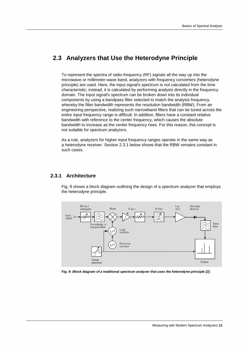
2.3 Analyzers that Use the Heterodyne Principle
To represent the spectra of radio-frequency (RF) signals all the way up into the
microwave or millimeter-wave band, analyzers with frequency converters (heterodyne
principle) are used. Here, the input signal's spectrum is not calculated from the time
characteristic; instead, it is calculated by performing analysis directly in the frequency
domain. The input signal's spectrum can be broken down into its individual
components by using a bandpass filter selected to match the analysis frequency,
whereby the filter bandwidth represents the resolution bandwidth (RBW). From an
engineering perspective, realizing such narrowband filters that can be tuned across the
entire input frequency range is difficult. In addition, filters have a constant relative
bandwidth with reference to the center frequency, which causes the absolute
bandwidth to increase as the center frequency rises. For this reason, this concept is
not suitable for spectrum analyzers.
As a rule, analyzers for higher input frequency ranges operate in the same way as
a heterodyne receiver. Section 2.3.1 below shows that the RBW remains constant in
such cases.
2.3.1 Architecture
Fig. 9 shows a block diagram outlining the design of a spectrum analyzer that employs
the heterodyne principle.
Fig. 9: Block diagram of a traditional spectrum analyzer that uses the heterodyne principle [2].
Basics of Spectral Analysis
Measuring with Modern Spectrum Analyzers 12
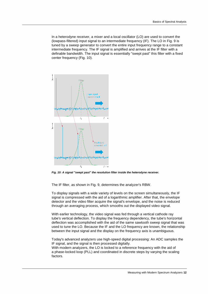
In a heterodyne receiver, a mixer and a local oscillator (LO) are used to convert the
(lowpass-filtered) input signal to an intermediate frequency (IF). The LO in Fig. 9 is
tuned by a sweep generator to convert the entire input frequency range to a constant
intermediate frequency. The IF signal is amplified and arrives at the IF filter with a
definable bandwidth. The input signal is essentially "swept past" this filter with a fixed
center frequency (Fig. 10).
Fig. 10: A signal "swept past" the resolution filter inside the heterodyne receiver.
The IF filter, as shown in Fig. 9, determines the analyzer's RBW.
To display signals with a wide variety of levels on the screen simultaneously, the IF
signal is compressed with the aid of a logarithmic amplifier. After that, the envelope
detector and the video filter acquire the signal's envelope, and the noise is reduced
through an averaging process, which smooths out the displayed video signal.
With earlier technology, the video signal was fed through a vertical cathode ray
tube's vertical deflection. To display the frequency dependency, the tube's horizontal
deflection was accomplished with the aid of the same sawtooth sweep signal that was
used to tune the LO. Because the IF and the LO frequency are known, the relationship
between the input signal and the display on the frequency axis is unambiguous.
Today's advanced analyzers use high-speed digital processing: An ADC samples the
IF signal, and the signal is then processed digitally.
With modern analyzers, the LO is locked to a reference frequency with the aid of
a phase-locked loop (PLL) and coordinated in discrete steps by varying the scaling
factors.
Basics of Spectral Analysis
Measuring with Modern Spectrum Analyzers 13
In addition, the video signal is prepared digitally, and a liquid-crystal display replaces
the cathode ray tube.
2.3.2 Frequency Selection
The following mathematical context applies when converting the input signal in the
mixer to the IF with the aid of an LO signal:
IFinLO ffnfm ||
(9)
Where
nm,
Natural numbers
inf
Frequency of the input signal to be converted
LOf
Frequency of the LO
IFf
IF
The following applies for the signal's fundamental (1st harmonic):
IFinLO fff ||
(10)
Or, when solving for inf
|| IFLOin fff
(11)
Taking a close look at Equation (11) reveals that for the oscillator frequencies and
IFs, two receiving frequencies always exist for which the criterion from Equation (10) is
fulfilled. This means that besides the desired input frequency range, there is another
one, the "image frequency band."
To ensure unambiguous results, possible input signals for the image frequencies must
be suppressed by employing corresponding filters ahead of the mixer's RF input.
Low IF
A spectrum analyzer should be able to process the widest possible input frequency
range; here, having a low IF leads to limitations:

Basics of Spectral Analysis
Measuring with Modern Spectrum Analyzers 14
If the input frequency range is greater than IFf2 , the input frequency and image
frequency ranges overlap (see Fig. 11).
Fig. 11: Low IF, large input-frequency range: The input and image frequency ranges overlap.
With the lower LO frequencies, a signal is received both from the green input
frequency range and from the red image frequency range. To achieve image frequency
rejection without harming the desired input signal, the input filter must be implemented
as a tunable bandpass filter. Doing so is highly complex from a technical standpoint.
Principle of using a high first IF
When a high first IF is used, the IF lies above the input frequency range.
Consequently, the image frequency range is then located above the input frequency
range. The two ranges do not overlap; therefore, image rejection can be accomplished
with a lowpass filter that has fixed tuning (see Fig. 12).
Fig. 12: The high-IF principle.
The following applies for conversion of the input signal:
inLOIF fff
(12)
Or for the image reception areas:

Basics of Spectral Analysis
Measuring with Modern Spectrum Analyzers 15
LOinIF fff
(13)
Basics of Spectral Analysis
Measuring with Modern Spectrum Analyzers 16
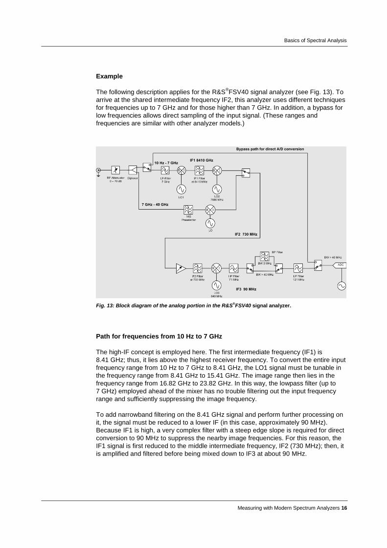
Example
The following description applies for the R&S®FSV40 signal analyzer (see Fig. 13). To
arrive at the shared intermediate frequency IF2, this analyzer uses different techniques
for frequencies up to 7 GHz and for those higher than 7 GHz. In addition, a bypass for
low frequencies allows direct sampling of the input signal. (These ranges and
frequencies are similar with other analyzer models.)
Fig. 13: Block diagram of the analog portion in the R&S®FSV40 signal analyzer.
Path for frequencies from 10 Hz to 7 GHz
The high-IF concept is employed here. The first intermediate frequency (IF1) is
8.41 GHz; thus, it lies above the highest receiver frequency. To convert the entire input
frequency range from 10 Hz to 7 GHz to 8.41 GHz, the LO1 signal must be tunable in
the frequency range from 8.41 GHz to 15.41 GHz. The image range then lies in the
frequency range from 16.82 GHz to 23.82 GHz. In this way, the lowpass filter (up to
7 GHz) employed ahead of the mixer has no trouble filtering out the input frequency
range and sufficiently suppressing the image frequency.
To add narrowband filtering on the 8.41 GHz signal and perform further processing on
it, the signal must be reduced to a lower IF (in this case, approximately 90 MHz).
Because IF1 is high, a very complex filter with a steep edge slope is required for direct
conversion to 90 MHz to suppress the nearby image frequencies. For this reason, the
IF1 signal is first reduced to the middle intermediate frequency, IF2 (730 MHz); then, it
is amplified and filtered before being mixed down to IF3 at about 90 MHz.
Basics of Spectral Analysis
Measuring with Modern Spectrum Analyzers 17
Path for frequencies above 7 GHz
The principle of using a high IF1 becomes increasingly difficult to implement as the
upper input frequency rises. For this reason, this principle is not used here for input
signals above 7 GHz; instead, those signals are converted directly to a low IF. Doing
this requires a tracking bandpass filter for image frequency rejection. Converting this
frequency range to a lower IF is possible because the frequency range from 7 GHz to
40 GHz covers less than a decade (the range from 10 Hz to 7 GHz, on the other hand,
corresponds to 8.8 decades), and YIG technology makes it possible to build a
narrowband bandpass filter that is tunable across this frequency range.
As with the lower frequencies, the frequencies above 7 GHz cannot be mixed down to
the desired low intermediate frequency IF3 (approximately 90 MHz), in a single step.
For this reason, these frequencies, too, are first converted to 730 MHz. After that, the
signal is amplified and coupled into the IF signal path for the low-frequency input stage.
Further processing of the IF2 signal is examined in Section 2.3.4.
2.3.3 Step-by-Step Tuning of the Local Oscillator (LO)
Due to the broad tuning range and low phase-noise that this technology offers, a YIG
oscillator is usually employed as the LO. Some spectrum analyzers also use voltage-
controlled oscillators (VCOs) for the LO.
In both cases, modern analyzers use a PLL to tie the oscillator to a reference signal.
That is the only way to achieve good frequency accuracy and
stability. Nevertheless, only discrete frequency steps are possible for this task.
Consequently, such analyzers can only be tuned in discrete steps.
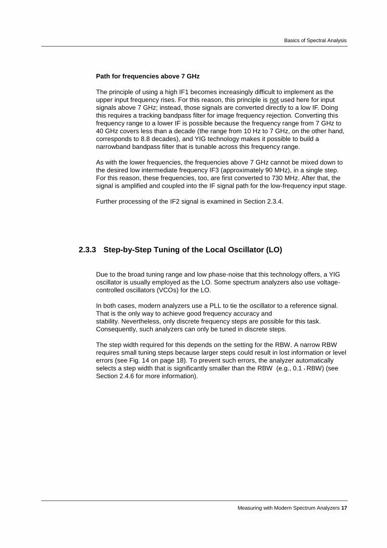
The step width required for this depends on the setting for the RBW. A narrow RBW
requires small tuning steps because larger steps could result in lost information or level
errors (see Fig. 14 on page 18). To prevent such errors, the analyzer automatically
selects a step width that is significantly smaller than the RBW (e.g., 0.1 * RBW) (see
Section 2.4.6 for more information).
Basics of Spectral Analysis
Measuring with Modern Spectrum Analyzers 18
Fig. 14: Effects of using a tuning step width that is too large: Left: Input signal is completely lost;
Right: Level errors arise in the representation of the input signal
2.3.4 Intermediate Frequency (IF) Signal Processing
The amplified and filtered IF2 signal with 730 MHz is converted to the IF3
(approximately 90 MHz), using the LO3 mixer.
In the IF3, the signal is amplified again in certain stages and limited to the selected
bandwidth by filters. Here, the amplification can be set in steps, which keeps the
maximum signal level constant in a way that is independent of the attenuator setting
and thus independent of the mixer level. The settings for the IF gain can be chosen to
allow the best possible exploitation of the ADC's dynamic range by setting the ADC's
maximum input level so that it corresponds to the level of the largest signal within the
IF bandwidth.
Depending on the concept used for the specific spectrum analyzer, with some
analyzers, users can influence this gain. This is usually done by selecting the reference
level. High reference levels result in a low IF gain; low reference levels result in high
gain. With some spectrum analyzers, however, the reference level setting is decoupled
from the IF gain, which means that the IF gain remains constant. In those cases,
changing the reference level only influences the representation of the signal on the
display through numeric scaling inside the computer.
With a traditional spectrum analyzer, the IF amplification is followed by what is referred
to as resolution filtering, which is defined by the selected RBW. The resolution filter
shows the portion of the input signal that was converted to the IF range and is to be
displayed at a specific point on the frequency axis.
Due to their steep edge slopes and the resulting spectral selection characteristics,
rectangular filters would be very well suited to serve as resolution filters. Due to their
long settling times, however, it would only be possible to tune the LO frequency very
slowly, as level errors could arise. That translates to long sweep times and slow
measurements.
Basics of Spectral Analysis
Measuring with Modern Spectrum Analyzers 19
Short measurement periods can be achieved by using Gaussian filters optimized for
settling times. Because – unlike rectangular filters – the transition from passband to
stopband is not abrupt, a definition must be found for the bandwidth. In general
spectral analysis, the 3 dB bandwidth is usually specified. This is the frequency
spacing between the two points for the transfer function that exhibit a magnitude
reduction of 3 dB compared with the transfer function for the center frequency.
When measuring noise signals or noise-like signals, one must reference the levels to
the measurement bandwidth, i.e., to the RBW. For this reason, the equivalent noise
bandwidth noiseB for the IF filter must be known, and it is calculated as follows:
dffHH
B V
V
noise )(1 2
2
0,
(14)
Where
noiseB Noise bandwidth, in Hz
)( fHV Voltage transfer function
0,VH Value of the voltage transfer function at the center frequency 0f
To visualize this, think of the noise bandwidth as the width of a rectangle that has the
same area as the area beneath the transfer function.
For measurements performed on correlated signals, such as the measurements
normally used with radar technology, for instance, the pulse bandwidth IB is also of
interest. Unlike the noise bandwidth, this bandwidth results from the integration of the
voltage transfer function. The following applies:
dffHH
B V
V
I )(1
0,
(15)
For Gaussian or Gaussian-like filters, the pulse bandwidth corresponds approximately
to the 6 dB bandwidth (which is customary in interference measurement equipment).
For test and measurement tasks, the correlations between 3 dB, 6 dB, noise, and
pulse bandwidths are of particular interest.
According to the Fourier transform, when a sinusoidal input signal is acquired with a
spectrum analyzer, an individual spectral line should appear on the screen at the signal
frequency. In reality, however, the resolution filter's transfer function appears. The
reason for this lies in the fact that the input signal that has been converted to the IF is
"swept past" the resolution filter during the sweep period and is multiplied with that
filter's transfer function (as in a convolution operation). It is also possible to think of this
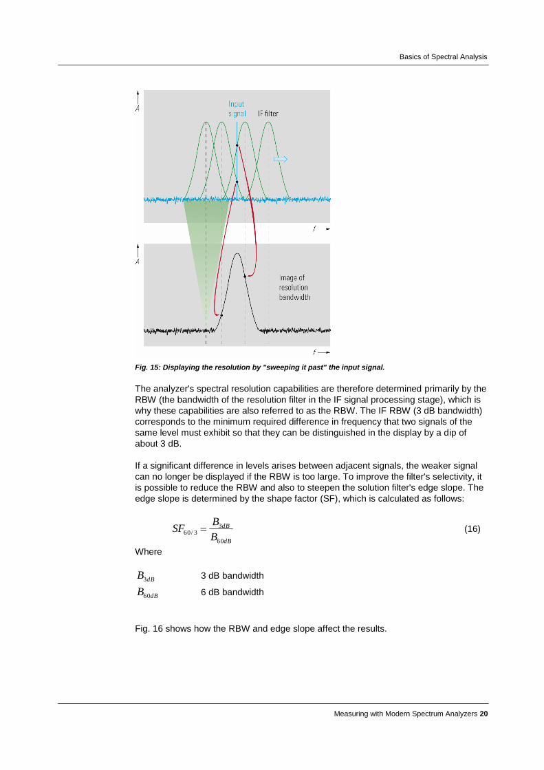
as the filter being "swept past" a fixed signal as shown in Fig. 15.
Basics of Spectral Analysis
Measuring with Modern Spectrum Analyzers 20
Fig. 15: Displaying the resolution by "sweeping it past" the input signal.
The analyzer's spectral resolution capabilities are therefore determined primarily by the
RBW (the bandwidth of the resolution filter in the IF signal processing stage), which is
why these capabilities are also referred to as the RBW. The IF RBW (3 dB bandwidth)
corresponds to the minimum required difference in frequency that two signals of the
same level must exhibit so that they can be distinguished in the display by a dip of
about 3 dB.
If a significant difference in levels arises between adjacent signals, the weaker signal
can no longer be displayed if the RBW is too large. To improve the filter's selectivity, it
is possible to reduce the RBW and also to steepen the solution filter's edge slope. The
edge slope is determined by the shape factor (SF), which is calculated as follows:
dB
dB
B
BSF
60
33/60
(16)
Where
dBB3 3 dB bandwidth
dBB60 6 dB bandwidth
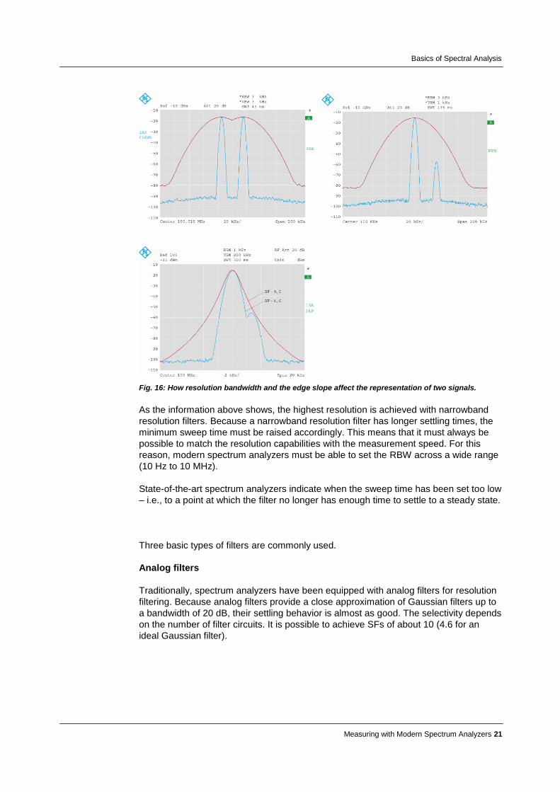
Fig. 16 shows how the RBW and edge slope affect the results.
Basics of Spectral Analysis
Measuring with Modern Spectrum Analyzers 21
Fig. 16: How resolution bandwidth and the edge slope affect the representation of two signals.
As the information above shows, the highest resolution is achieved with narrowband
resolution filters. Because a narrowband resolution filter has longer settling times, the
minimum sweep time must be raised accordingly. This means that it must always be
possible to match the resolution capabilities with the measurement speed. For this
reason, modern spectrum analyzers must be able to set the RBW across a wide range
(10 Hz to 10 MHz).
State-of-the-art spectrum analyzers indicate when the sweep time has been set too low
– i.e., to a point at which the filter no longer has enough time to settle to a steady state.
Three basic types of filters are commonly used.
Analog filters
Traditionally, spectrum analyzers have been equipped with analog filters for resolution
filtering. Because analog filters provide a close approximation of Gaussian filters up to
a bandwidth of 20 dB, their settling behavior is almost as good. The selectivity depends
on the number of filter circuits. It is possible to achieve SFs of about 10 (4.6 for an
ideal Gaussian filter).
Basics of Spectral Analysis
Measuring with Modern Spectrum Analyzers 22
Even advanced spectrum analyzers that already work with digital filters (see below)
do not go completely without analog filters. With an analyzer built as depicted in Fig. 13
(page xx), an analog prefilter with a bandwidth of approximately 3 MHz is switched into
the IF3 signal path when small RBWs are used. This prefilter suppresses large signals
located outside of the RBW being observed, making it possible to employ a higher IF
gain without overamplifying the ADC. The prefilter also lowers the noise bandwidth and
suppresses undesired intermodulation products from the upstream mixing stages.
These two aspects lead to a larger spurious-free dynamic range (SFDR).
Digital filters
Current digital signal processing makes it easy to achieve all required bandwidths, i.e.,
1 Hz to more than 50 MHz. In this way, designing ideal Gaussian filters (SF = 4.6) is
possible, thus achieving better selectivity than is possible when analog filters are
employed (at a reasonable expense). Beyond that, digital filters do not have to be
aligned; they remain stable across a range of temperatures, and they are not subject
to aging – all of which enables them to achieve greater bandwidth accuracy.
The settling time of a digital filter is always given. Correction calculations make it
possible to shorten the sweep time – without changing the RBW – to a greater extent
than is possible with analog filters.
Because digital filters do not have to be implemented in hardware, many different filter
types can be made available on a spectrum analyzer. For instance, in addition to
Gaussian filters, rectangular filters can be provided for signal analysis
(demodulation).
Using FFT
This is not filtering in the traditional sense, but rather a combination of a tuned
spectrum analyzer and an FFT analyzer. Here, small subranges of the spectrum to be
represented are calculated using FFTs. For further details on this operating mode, see
Section 2.4.
2.3.5 Envelope Detection and Video Filter
As with amplitude-modulated signals, the information on the input signal's level is
contained in the level of the IF signal, in its envelope. For this reason, after resolution
filtering is performed on the last IF, the system determines this IF signal's envelope.
The procedure for doing this compares to demodulation of an AM signal, which means,
for instance, that an analog envelope demodulator can be used. Here, the IF signal is
rectified, and the RF signal components can be eliminated by a lowpass filter. The
"video voltage" then arises at the output.
Basics of Spectral Analysis
Measuring with Modern Spectrum Analyzers 23
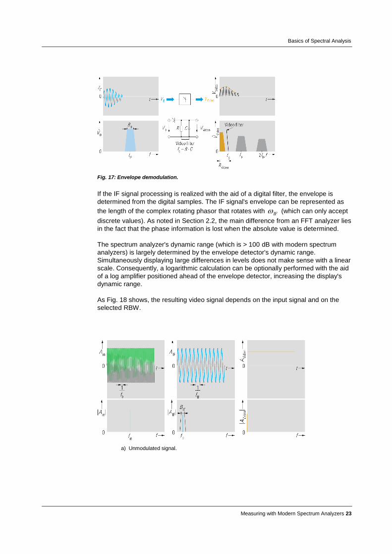
Fig. 17: Envelope demodulation.
If the IF signal processing is realized with the aid of a digital filter, the envelope is
determined from the digital samples. The IF signal's envelope can be represented as
the length of the complex rotating phasor that rotates with IF (which can only accept
discrete values). As noted in Section 2.2, the main difference from an FFT analyzer lies
in the fact that the phase information is lost when the absolute value is determined.
The spectrum analyzer's dynamic range (which is > 100 dB with modern spectrum
analyzers) is largely determined by the envelope detector's dynamic range.
Simultaneously displaying large differences in levels does not make sense with a linear
scale. Consequently, a logarithmic calculation can be optionally performed with the aid
of a log amplifier positioned ahead of the envelope detector, increasing the display's
dynamic range.
As Fig. 18 shows, the resulting video signal depends on the input signal and on the
selected RBW.
a) Unmodulated signal.
Basics of Spectral Analysis
Measuring with Modern Spectrum Analyzers 24
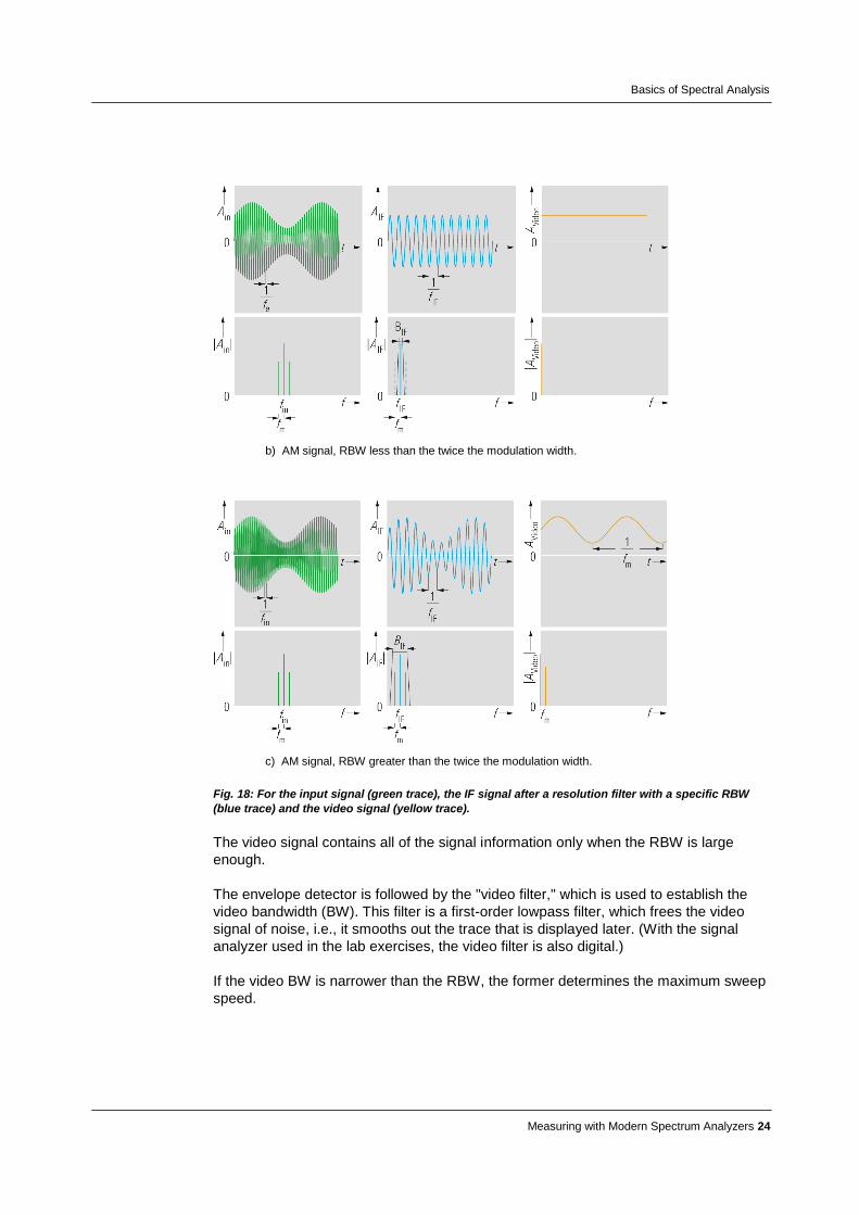
b) AM signal, RBW less than the twice the modulation width.
c) AM signal, RBW greater than the twice the modulation width.
Fig. 18: For the input signal (green trace), the IF signal after a resolution filter with a specific RBW
(blue trace) and the video signal (yellow trace).
The video signal contains all of the signal information only when the RBW is large
enough.
The envelope detector is followed by the "video filter," which is used to establish the
video bandwidth (BW). This filter is a first-order lowpass filter, which frees the video
signal of noise, i.e., it smooths out the trace that is displayed later. (With the signal
analyzer used in the lab exercises, the video filter is also digital.)
If the video BW is narrower than the RBW, the former determines the maximum sweep
speed.
Basics of Spectral Analysis
Measuring with Modern Spectrum Analyzers 25
Fig. 18 shows that the video BW should be set to suit the current measurement
application: When measuring sinusoidal signals with a sufficient signal-to-noise ratio,
the video BW is selected to be the same as the RBW. If the signal-to-noise ratio
decreases, the noise can be averaged by reducing the video BW, thus making it
possible to achieve a significantly more stable display. (If the video BW is selected to
be lower than the bandwidth of the signal to be displayed, the system no longer
displays the entire spectrum, which means that information is lost.)
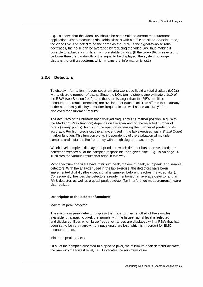
2.3.6 Detectors
To display information, modern spectrum analyzers use liquid crystal displays (LCDs)
with a discrete number of pixels. Since the LO's tuning step is approximately 1/10 of
the RBW (see Section 2.4.2), and the span is larger than the RBW, multiple
measurement results (samples) are available for each pixel. This affects the accuracy
of the numerically displayed marker frequencies as well as the accuracy of the
displayed measurement results.
The accuracy of the numerically displayed frequency at a marker position (e.g., with
the Marker to Peak function) depends on the span and on the selected number of
pixels (sweep points). Reducing the span or increasing the number of pixels boosts
accuracy. For high precision, the analyzer used in the lab exercises has a Signal Count
marker function. This function works independently of the evaluation of multiple
samples and indicates the frequency with a high degree of accuracy.
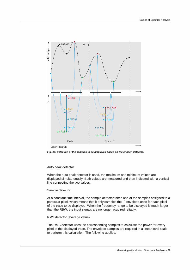
Which level sample is displayed depends on which detector has been selected; the
detector assesses all of the samples responsible for a given pixel. Fig. 19 on page 26
illustrates the various results that arise in this way.
Most spectrum analyzers have minimum peak, maximum peak, auto peak, and sample
detectors. With the analyzer used in the lab exercise, the detectors have been
implemented digitally (the video signal is sampled before it reaches the video filter).
Consequently, besides the detectors already mentioned, an average detector and an
RMS detector, as well as a quasi-peak detector (for interference measurements), were
also realized.
Description of the detector functions
Maximum peak detector
The maximum peak detector displays the maximum value. Of all of the samples
available for a specific pixel, the sample with the largest signal level is selected
and displayed. Even when large frequency ranges are displayed with a RBW that has
been set to be very narrow, no input signals are lost (which is important for EMC
measurements).
Minimum peak detector
Of all of the samples allocated to a specific pixel, the minimum peak detector displays
the one with the lowest level, i.e., it indicates the minimum value.
Basics of Spectral Analysis
Measuring with Modern Spectrum Analyzers 26
Fig. 19: Selection of the samples to be displayed based on the chosen detector.
Auto peak detector
When the auto peak detector is used, the maximum and minimum values are
displayed simultaneously. Both values are measured and then indicated with a vertical
line connecting the two values.
Sample detector
At a constant time interval, the sample detector takes one of the samples assigned to a
particular pixel, which means that it only samples the IF envelope once for each pixel
of the trace to be displayed. When the frequency range to be displayed is much larger
than the RBW, the input signals are no longer acquired reliably.
RMS detector (average value)
The RMS detector uses the corresponding samples to calculate the power for every
pixel of the displayed trace. The envelope samples are required in a linear level scale
to perform this calculation. The following applies:
Basics of Spectral Analysis
Measuring with Modern Spectrum Analyzers 27
N
i
iRMS vN
V1
21 (17)
Where
RMSV = RMS value for the voltage, in V
N = Number of samples that are allocated to a pixel
iv = Samples for the envelope, in V
The power at the reference impedance is:
R
VP RMS
2
(18)
Average (AV) detector
The AV detector calculates the linear average for each pixel of the displayed trace from
the corresponding samples. The envelope samples are required in a linear level scale
to perform this calculation. The following applies:
N
i
iAV vN
V1
1 (19)
AVV = Average voltage, in V
Quasi-peak detector
The quasi-peak detector detects the peaks for interference measurements with a
defined charge and discharge time. It is used to measure electromagnetic interference.
How detectors affect representation of different input signals
Depending on the input signal, the different detectors lead to different measurement
results. For sinusoidal input signals with a sufficient signal-to-noise ratio, the video
voltage is constant. The level of the displayed signal is therefore independent of the
selected detector because all samples have the same level, and the values (RMS, AV)
calculated from them correspond to the level of each individual sample.
With random signals such as noise or noise-like signals, the instantaneous power
varies over time, which means that the maximum and minimum instantaneous values
as well as the average and RMS values for the envelope differ. The power for signals
with a limited observation period T is calculated as follows:
Basics of Spectral Analysis
Measuring with Modern Spectrum Analyzers 28
dttvTR
PTt
Tt
2/
2/
2 )(11
(20)
Furthermore, during the observation period TI, the peak for the instantaneous power
can be determined and that value used to calculate the crest factor.
)lg(10CFRMS
peak
P
P
(21)
Where
CF
Crest factor, in dB
peakP Peak power during the observation period T, in W
RMSP RMS power, in W
With a pure noise signal, it is theoretically possible for all voltages to occur (the crest
factor can be of any size). Nevertheless, the probability that very high or very low
voltage values will arise is very low. Consequently, in practice, values that can be
displayed are achievable when the observation periods are long enough (e.g., crest
factor = 12 dB for Gaussian noise).
How the selected detector and the sweep time influence the display of stochastic
signals
Maximum peak detector
The system responds too strongly to stochastic signals; they result in the highest
level display. If the sweep time increases, the dwell time in a frequency range assigned
to a pixel rises. This increases the probability of higher instantaneous values, and the
levels of the displayed pixels rise.
Using short sweep times delivers the same display as with the sample detector
because only one sample is recorded per pixel.
Minimum peak detector
The minimum peak detector can be considered in the same way as the maximum peak
detector, but for low signal levels.
Auto peak detector
The results of the maximum peak and minimum peak detectors are connected with a
line and displayed simultaneously. If the sweep time increases, the displayed noise
bandwidth becomes significantly larger.
Basics of Spectral Analysis
Measuring with Modern Spectrum Analyzers 29
Sample detector
Because only one sample is used at a defined time, the displayed trace varies due to
the distribution of the instantaneous value around the average value for the envelope
of the IF signal that results from the noise. In the case of Gaussian noise, this average
value is 1.05 dB below the RMS value (also, using a narrow video BW in the
logarithmic scale results in display values that are lower by an additional 1.45 dB).
Thus, the displayed noise is a total of 2.5 dB below the RMS value.
With this detector, changing the sweep time does not affect the display because the
number of evaluated samples is constant.
RMS detector
An input signal's actual power can be measured independently of its time variation.
When the signal power is determined using data from the sample detector or maximum
peak detector, the parameters for signal statistics must be known if working with
stochastic signals. This information is not needed when the RMS detector is used.
Increasing the sweep time also increases the number of samples that enter the
calculation, which smooths out the displayed trace. Because averaging through a
narrow video BW falsifies the RMS display, the video BW must be at least three times
as large as the RBW.
AV detector
In the linear level scale, an input signal's actual average value can be measured
independently of its time variation. When averaging logarithmic values, the display
level determined in this way would be too low because higher signal values are
subjected to greater compression. Raising the sweep time makes more samples
available per pixel for the calculation, which smooths out the displayed trace.
Using linear levels at the video filter's input and reducing the video BW will smoothen
the signal.
As mentioned above, reducing the video BW smooths out the trace display through
averaging. The prerequisite for this, however, is that the signal levels ahead of the
envelope detector or video filter must be in the linear scale. The resulting display then
represents the actual average value. If, on the other hand, the IF signal is
logarithmized, the displayed average value is lower than the actual average value.
Marker functions
The Marker to Peak and Signal Count marker functions make it possible to work with a
limited screen resolution and to read measurement results at a substantially higher
resolution.

Basics of Spectral Analysis
Measuring with Modern Spectrum Analyzers 30
2.4 Combining Both Implementation Approaches
As explained in Sections 2.2 and 2.3, both FFT analyzers and spectrum analyzers that
use the heterodyne principle offer specific advantages.
The benefits of using an FFT analyzer include the use of high measurement speeds at
low RBWs and the ability to record the signal in the time domain with all of the phase
information. This makes it possible to also analyze complex modulations (signal
analysis).
An advantage of spectrum analyzers that employ the heterodyne scheme is that the
input frequency range is independent of the ADC rate. When preselection is used,
excellent suppression of harmonics and of other undesired spectral components can
be achieved.
All of these benefits can be realized by skillfully combining an FFT analyzer with a
traditional spectrum analyzer. One of the key features of modern analyzers is that
many of the processing steps performed by traditional analog spectrum analyzers are
now digitalized, meaning that they are implemented in software or digital hardware
(such as an FPGA or ASIC). To provide sufficient dynamic range, ADCs that allow a
high quantization depth are used for this.
Fig. 20 on page 31 shows the analog portion of a modern analyzer. Its functions
correspond to those of a heterodyne spectrum analyzer – until the last IF stage. After
that, further processing is accomplished digitally.
As with FFT analyzers, a sampled time-domain signal is made available after A/D
conversion. That opens up the possibility for signal analysis, i.e., for demodulation of
the signal. (The IF3 signal's bandwidth amounts to more than 40 MHz, making it
possible to acquire data in the formats employed for all commonly used
communications standards and then demodulate and analyze that information using
the corresponding software options. For this reason, modern spectrum analyzers are
often referred to as "signal and spectrum analyzers." Nevertheless, the focus here will
remain on "spectral analysis.")
The ADC in Fig. 20 on page 31 does not sample a baseband signal, but rather an IF
signal. The system performs bandpass sampling, i.e., it samples a signal associated
with bandwidth B. The sampling rate used here can be even lower than the level of
twice the largest frequency that arises (IF3+B/2). Nonetheless, the sampling rate must
at least meet the Nyquist criterion for the signal bandwidth (i.e., it must be larger than
2*B). For the analyzer outlined in Fig. 20, the bandpass filtering is realized before
sampling through use of the 71 MHz highpass filter and the 121 MHz lowpass filter.
The result of the bandpass sampling is a time-discrete and value-discrete IF signal. In
another processing step, "digital down-conversion" is used to generate a complex
baseband signal from this digital IF signal.
Basics of Spectral Analysis
Measuring with Modern Spectrum Analyzers 31
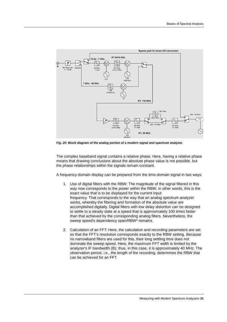
Fig. 20: Block diagram of the analog portion of a modern signal and spectrum analyzer.
The complex baseband signal contains a relative phase. Here, having a relative phase
means that drawing conclusions about the absolute phase value is not possible, but
the phase relationships within the signals remain constant.
A frequency-domain display can be prepared from the time-domain signal in two ways:
1. Use of digital filters with the RBW: The magnitude of the signal filtered in this
way now corresponds to the power within the RBW; in other words, this is the
exact value that is to be displayed for the current input
frequency. That corresponds to the way that an analog spectrum analyzer
works, whereby the filtering and formation of the absolute value are
accomplished digitally. Digital filters with low delay distortion can be designed
to settle to a steady state at a speed that is approximately 100 times faster
than that achieved by the corresponding analog filters. Nevertheless, the
sweep speed's dependency span/RBW² remains.
2. Calculation of an FFT: Here, the calculation and recording parameters are set
so that the FFT's resolution corresponds exactly to the RBW setting. Because
no narrowband filters are used for this, their long settling time does not
dominate the sweep speed. Here, the maximum FFT width is limited by the
analyzer's IF bandwidth (B); thus, in this case, it is approximately 40 MHz. The
observation period, i.e., the length of the recording, determines the RBW that
can be achieved for an FFT.
Basics of Spectral Analysis
Measuring with Modern Spectrum Analyzers 32
In both cases, it is necessary to "run through" the frequency range that has been set
on the analyzer. With the first variant, this is done in very small steps: fStep << RBW.
That corresponds to the method described for traditional spectrum analyzers. With the
second variant, the selected step width can be as large as the RBW. This means that
the number of span/RBW FFT calculations can cover a specific span. Consequently,
the sweep time is no longer proportional to span/RBW². For this reason, the variant for
settings with a small RBW is particularly well suited for this task.
Modern spectrum analyzers take advantage of the fact that the input signal can be
switched directly to the ADC. The bypass in Fig. 20 is meant to accomplish this. Such
direct sampling offers the advantage that neither mixers nor LOs influence the signal to
be measured. This concept offers special advantages for noise and phase noise
measurements: Using the direct path makes it possible to use a mid-range spectrum
analyzer to measure signals that have a phase noise less than –130 dBc/Hz at a
10 kHz offset.
Direct sampling is, however, restricted to frequencies lower than half the sampling rate
for the ADC being used. Depending on the settings, the spectrum analyzer used for the
lab exercises employs this possibility up to frequencies just higher than 20 MHz.
2.5 Important Terms and Settings
Frequency range to be displayed
The frequency range to be displayed can be set either by using the start and stop
frequencies or by using the center frequency and the span.
Level range to be displayed
This range is set by establishing the maximum level to be displayed (referred to as the
reference level) and by establishing the span. The levels can be displayed in the linear
or logarithmic scale. The damping of the attenuator on the input end also depends on
these settings.
Attenuator
To be able to display high signal levels, the spectrum analyzer's input has been
equipped with an attenuator set in steps. This attenuator can be used to set the signal
level at the input for the first mixer – the mixer level.
Frequency resolution
With analyzers that employ the heterodyne principle, the frequency resolution is set via
the resolution filter's bandwidth (see Section 2.3), referred to as the RBW.
Sweep time (only for analyzers that employ the heterodyne principle)
This is the time required to record the entire relevant frequency spectrum. The shortest
sweep time is set automatically by the analyzer software, based on the selected
bandwidths (RBW and video BW).
Basics of Spectral Analysis
Measuring with Modern Spectrum Analyzers 33
Dependencies for the sweep time, span or RBW and video BW
The shortest permissible sweep time is derived from the settling time of the resolution
filter and the video filter. The video filter only influences the sweep time if the video BW
is smaller than the RBW. This is expressed by the following equation:
2B
fkTsweep
(22)
Where
sweepT
Minimum required sweep time (for the given span and RBW), in s
B RBW if RBW ≤ Video BW
Video BW if Video BW ≤ RBW
f Frequency range to be displayed (span)
k Proportionality factor, depending on the type of filter and on the required level
accuracy.
Generators and Their Use
Measuring with Modern Spectrum Analyzers 34
3 Generators and Their Use
RF generators are classified into two main types:
Analog signal generators
Vector signal generators
Many other possible classifications exist based on various characteristics: frequency
range or output power, form factor, capabilities for remote control, power supply, and
others. This document will not examine those classifications.
Analog and vector signal generators generate their output signals in completely
different ways, resulting in different modulation types and applications.
3.1 Analog Signal Generators
With analog signal generators, the focus is on generating a high-quality RF signal.
These devices support the analog modulation types: AM / FM and φM. Some devices
can also be used to generate precise pulsed signals.
Analog generators are available for frequencies extending up to the microwave range.
Their distinguishing features are:
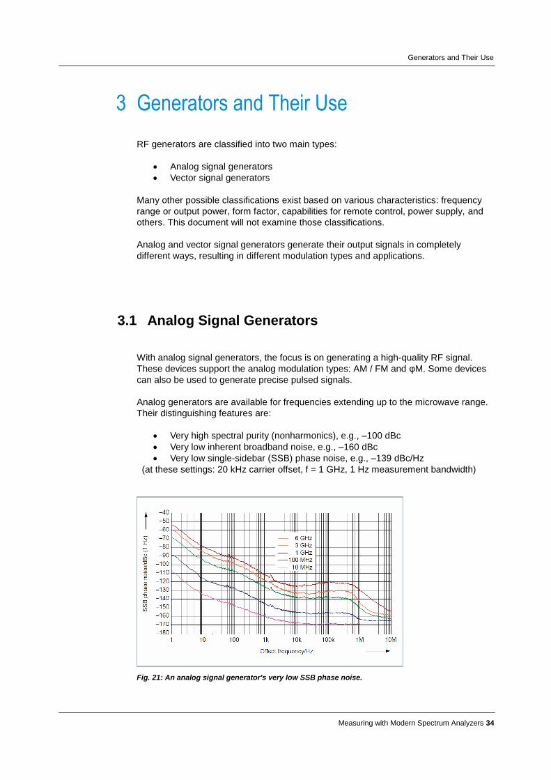
Very high spectral purity (nonharmonics), e.g., –100 dBc
Very low inherent broadband noise, e.g., –160 dBc
Very low single-sidebar (SSB) phase noise, e.g., –139 dBc/Hz
(at these settings: 20 kHz carrier offset, f = 1 GHz, 1 Hz measurement bandwidth)
Fig. 21: An analog signal generator's very low SSB phase noise.
Generators and Their Use
Measuring with Modern Spectrum Analyzers 35
Analog signal generators are used:
As stable reference signals (local oscillator [LO], source for measuring phase
noise, or as a calibration reference)
As a universal instrument for measuring gain, linearity, bandwidth, etc.
In the development and testing of RF chips and other semiconductor chips,
such as those used for ADCs
For receiver tests (two-tone tests, generation of interferer, and blocking
signals)
For EMC tests
For automated test equipment (ATE) and production
For avionics applications (such as VOR, ILS)
For military applications
For radar tests
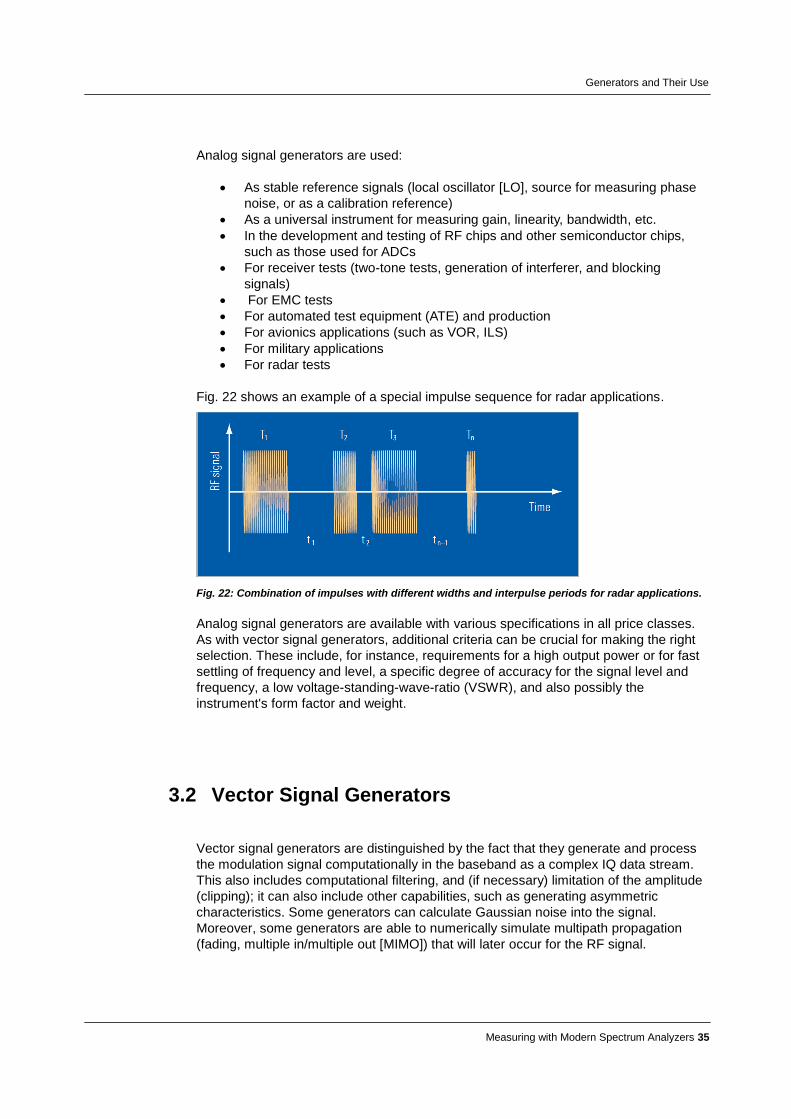
Fig. 22 shows an example of a special impulse sequence for radar applications.
Fig. 22: Combination of impulses with different widths and interpulse periods for radar applications.
Analog signal generators are available with various specifications in all price classes.
As with vector signal generators, additional criteria can be crucial for making the right
selection. These include, for instance, requirements for a high output power or for fast
settling of frequency and level, a specific degree of accuracy for the signal level and
frequency, a low voltage-standing-wave-ratio (VSWR), and also possibly the
instrument's form factor and weight.
3.2 Vector Signal Generators
Vector signal generators are distinguished by the fact that they generate and process
the modulation signal computationally in the baseband as a complex IQ data stream.
This also includes computational filtering, and (if necessary) limitation of the amplitude
(clipping); it can also include other capabilities, such as generating asymmetric
characteristics. Some generators can calculate Gaussian noise into the signal.
Moreover, some generators are able to numerically simulate multipath propagation
(fading, multiple in/multiple out [MIMO]) that will later occur for the RF signal.

Generators and Their Use
Measuring with Modern Spectrum Analyzers 36
In general, the complete generation of the baseband signal is accomplished through
real-time computation. Arbitrary waveform generators (AWGs) are an exception to this
(see Section 3.3).
Generators and Their Use
Measuring with Modern Spectrum Analyzers 37
The baseband IQ data are ultimately converted to an RF operating frequency. (Some
vector generators operate exclusively in the baseband without generating RF signals.)
Often, vector signal generators are also equipped with analog or digital IQ inputs to
feed external baseband signals into the instrument.
Using IQ technology makes it possible to realize any modulation types – whether
simple or complex, digital or analog – as well as single-carrier and multicarrier signals.
The requirements that the vector signal generators must meet are primarily derived
from the requirements established by wireless communications standards, but also
from digital broadband cable transmission and from A&D applications (generation of
modulated pulses).
The main areas of application for vector signal generators are:
Generating standards-compliant signals for wireless communications, digital
radio and TV, GPS, modulated radar, etc.
Testing digital receivers or modules in development and manufacturing
Simulating signal impairments (noise, fading, clipping, insertion of bit errors)
Generating signals for multi-antenna systems (MIMO), with and without phase
coherence for beam forming
Generating modulated sources of interference for blocking tests and for
measuring suppression of adjacent channels
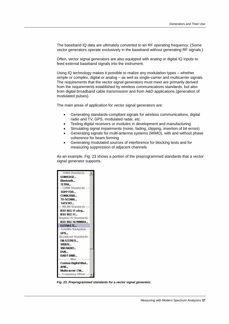
As an example, Fig. 23 shows a portion of the preprogrammed standards that a vector
signal generator supports.
Fig. 23: Preprogrammed standards for a vector signal generator.
Generators and Their Use
Measuring with Modern Spectrum Analyzers 38
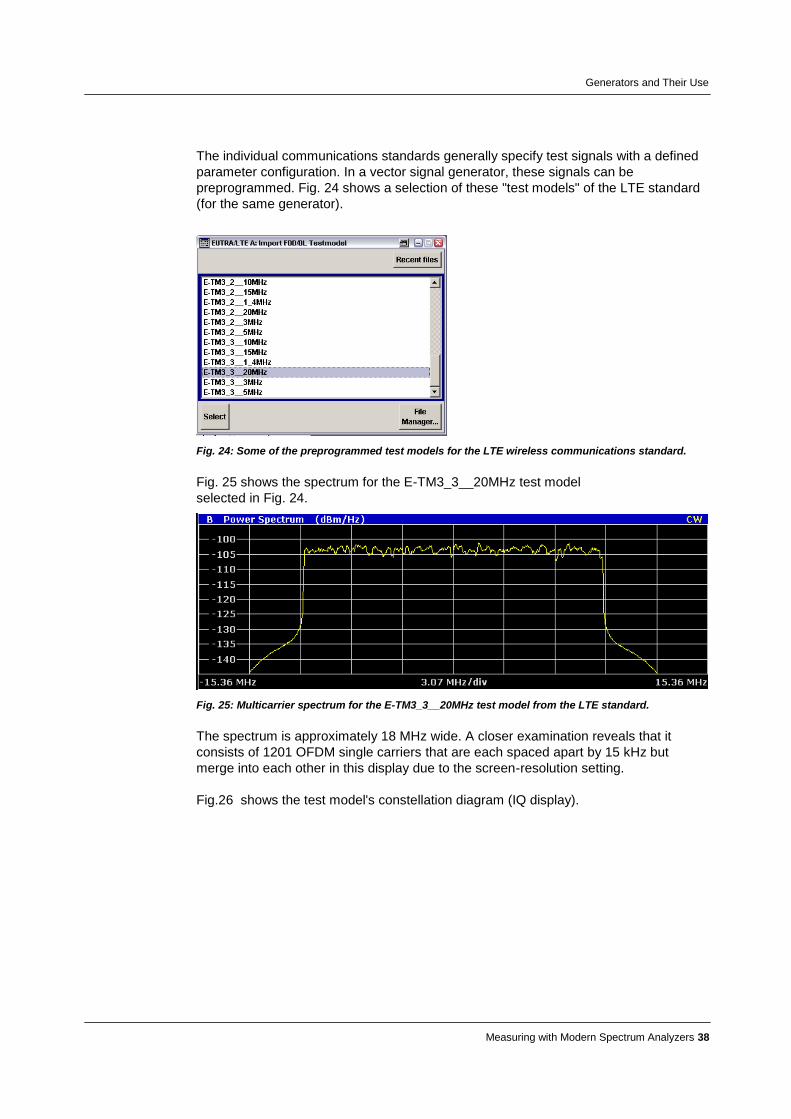
The individual communications standards generally specify test signals with a defined
parameter configuration. In a vector signal generator, these signals can be
preprogrammed. Fig. 24 shows a selection of these "test models" of the LTE standard
(for the same generator).
Fig. 24: Some of the preprogrammed test models for the LTE wireless communications standard.
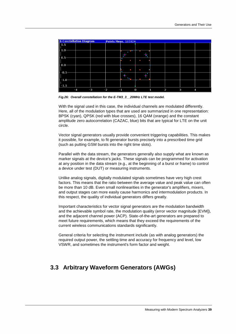
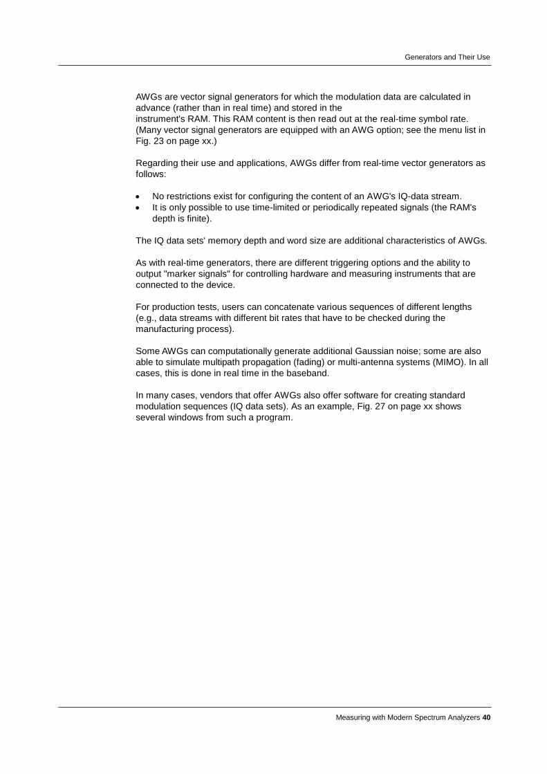
Fig. 25 shows the spectrum for the E-TM3_3__20MHz test model
selected in Fig. 24.
Fig. 25: Multicarrier spectrum for the E-TM3_3__20MHz test model from the LTE standard.
The spectrum is approximately 18 MHz wide. A closer examination reveals that it
consists of 1201 OFDM single carriers that are each spaced apart by 15 kHz but
merge into each other in this display due to the screen-resolution setting.
Fig.26 shows the test model's constellation diagram (IQ display).
Generators and Their Use
Measuring with Modern Spectrum Analyzers 39
Fig.26: Overall constellation for the E-TM3_3__20MHz LTE test model.
With the signal used in this case, the individual channels are modulated differently.
Here, all of the modulation types that are used are summarized in one representation:
BPSK (cyan), QPSK (red with blue crosses), 16 QAM (orange) and the constant
amplitude zero autocorrelation (CAZAC, blue) bits that are typical for LTE on the unit
circle.
Vector signal generators usually provide convenient triggering capabilities. This makes
it possible, for example, to fit generator bursts precisely into a prescribed time grid
(such as putting GSM bursts into the right time slots).
Parallel with the data stream, the generators generally also supply what are known as
marker signals at the device's jacks. These signals can be programmed for activation
at any position in the data stream (e.g., at the beginning of a burst or frame) to control
a device under test (DUT) or measuring instruments.
Unlike analog signals, digitally modulated signals sometimes have very high crest
factors. This means that the ratio between the average value and peak value can often
be more than 10 dB. Even small nonlinearities in the generator's amplifiers, mixers,
and output stages can more easily cause harmonics and intermodulation products. In
this respect, the quality of individual generators differs greatly.
Important characteristics for vector signal generators are the modulation bandwidth
and the achievable symbol rate, the modulation quality (error vector magnitude [EVM]),
and the adjacent channel power (ACP). State-of-the-art generators are prepared to
meet future requirements, which means that they exceed the requirements of the
current wireless communications standards significantly.
General criteria for selecting the instrument include (as with analog generators) the
required output power, the settling time and accuracy for frequency and level, low
VSWR, and sometimes the instrument's form factor and weight.
3.3 Arbitrary Waveform Generators (AWGs)
Generators and Their Use
Measuring with Modern Spectrum Analyzers 40
AWGs are vector signal generators for which the modulation data are calculated in
advance (rather than in real time) and stored in the
instrument's RAM. This RAM content is then read out at the real-time symbol rate.
(Many vector signal generators are equipped with an AWG option; see the menu list in
Fig. 23 on page xx.)
Regarding their use and applications, AWGs differ from real-time vector generators as
follows:
No restrictions exist for configuring the content of an AWG's IQ-data stream.
It is only possible to use time-limited or periodically repeated signals (the RAM's
depth is finite).
The IQ data sets' memory depth and word size are additional characteristics of AWGs.
As with real-time generators, there are different triggering options and the ability to
output "marker signals" for controlling hardware and measuring instruments that are
connected to the device.
For production tests, users can concatenate various sequences of different lengths
(e.g., data streams with different bit rates that have to be checked during the
manufacturing process).
Some AWGs can computationally generate additional Gaussian noise; some are also
able to simulate multipath propagation (fading) or multi-antenna systems (MIMO). In all
cases, this is done in real time in the baseband.
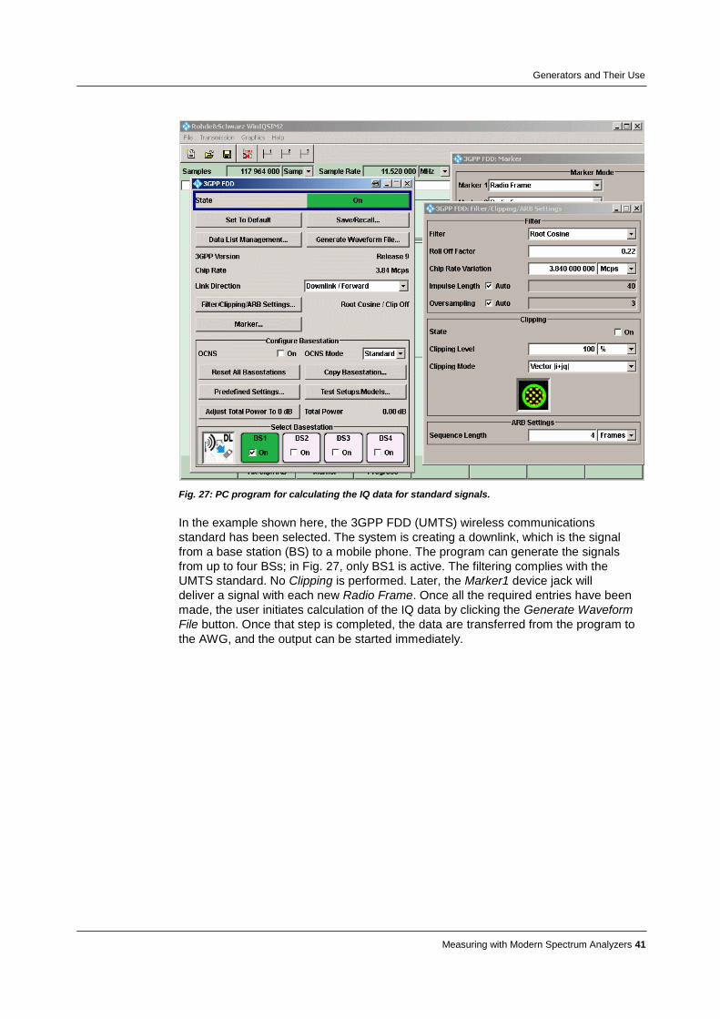
In many cases, vendors that offer AWGs also offer software for creating standard
modulation sequences (IQ data sets). As an example, Fig. 27 on page xx shows
several windows from such a program.
Generators and Their Use
Measuring with Modern Spectrum Analyzers 41
Fig. 27: PC program for calculating the IQ data for standard signals.
In the example shown here, the 3GPP FDD (UMTS) wireless communications
standard has been selected. The system is creating a downlink, which is the signal
from a base station (BS) to a mobile phone. The program can generate the signals
from up to four BSs; in Fig. 27, only BS1 is active. The filtering complies with the
UMTS standard. No Clipping is performed. Later, the Marker1 device jack will
deliver a signal with each new Radio Frame. Once all the required entries have been
made, the user initiates calculation of the IQ data by clicking the Generate Waveform
File button. Once that step is completed, the data are transferred from the program to
the AWG, and the output can be started immediately.
Nonlinearities of the Device under Test (DUT)
Measuring with Modern Spectrum Analyzers 42
4 Nonlinearities of the Device under Test (DUT) For the most part, the structure and content of this chapter have been taken from
the lecture notes on practical exercises entitled "Hochfrequenztechnik Labor,
Spektrumanalysator'' from the University of Graz, Austria [2]. Further information is
available, for instance, in the white paper "Interaction of Intermodulation Products
between DUT and Spectrum Analyzer" [4].
An ideal two-port device transfers signals from the input to the output without distorting
them. The output signal follows any variation in the input signal in strict proportion.
Only the same frequencies that are fed into the input arise at the output.
The DUT, a real amplifier, is not an ideal two-port:
1. As the input power rises, the effective power gain decreases.
2. In addition, the higher-order harmonics and the intermodulation products from the
input frequencies and their harmonics rise at the output.
This first observation describes an amplifier's large-signal behavior. Above a certain
input level, the amplifier reaches saturation. The maximum permissible input level is
defined by the 1 dB compression point.
The second observation describes the small-signal distortions that always arise. Even
when driven with small signals, an amplifier's characteristic curve is never purely
linear. The fact that spectral components that were not present in the input signal arise
in the output signal can be substantiated mathematically. Specifying intercept points
makes it possible to compare amplifiers and to properly dimension hardware setups.
(The fact that new spectral components arise at nonlinearities is, to some extent,
employed intentionally in RF engineering, e.g., to multiply frequencies on a diode
characteristic curve or to convert frequencies in mixers.)
4.1 1 dB Compression Point
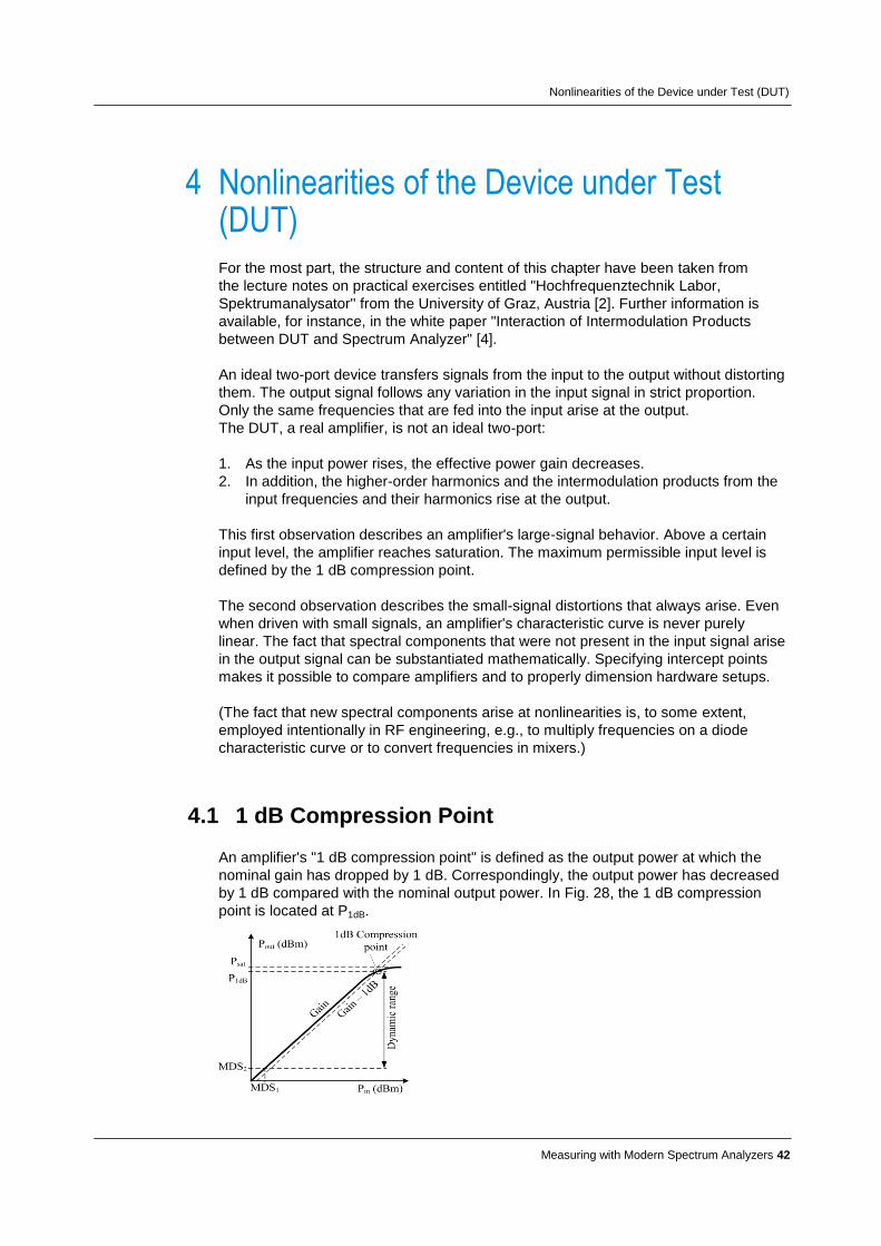
An amplifier's "1 dB compression point" is defined as the output power at which the
nominal gain has dropped by 1 dB. Correspondingly, the output power has decreased
by 1 dB compared with the nominal output power. In Fig. 28, the 1 dB compression
point is located at P1dB.
Nonlinearities of the Device under Test (DUT)
Measuring with Modern Spectrum Analyzers 43
Fig. 28: Correlation between the input power ( inP ) and output power ( outP ) of an amplifier
(logarithmic scale) with the 1 dB compression point.
The low end of the linear dynamic range is limited by the smallest signal power that
can be differentiated from noise at the system's input. There must be a "minimum
detectable signal" ( 1MDS ) present that is x dB larger than the unavoidable thermal
noise floor (–174 dBm per Hz at 290 kbit). For most applications, the minimum signal
power should be twice as large as the noise power; thus, x dB = 3 dB. When, however,
we take the amplifier's actual bandwidth B and noise factor F into account, we arrive at
the following:
xFBdBmMDS log10log101741 (23)
The following then holds true for the power that arises at the output in combination with
gain G :
GxFBdBmMDS log10log10log101742 (24)
When the level is rising, the 1 dB compression point defines the end of the linear area.
The output power P1dB supplied at this point is normally indicated in product data
sheets as the maximum power that the amplifier can deliver.
dBGPP dBindB 1log1011 (25)
The amplifier's linear dynamic range D is now the decrease in amplitude between the
1 dB compression point and the power generated at the output 2MDS [2]:
GxFBdBmdBmPdBD dB log10log10log10174)()( 1 (26)
The more an amplifier is operated in the range that is no longer linear, the more the
output power is spread into harmonics and intermodulation products. Power is then
"shifted" to spectral components other than the ones that originally had the power (see
the introduction to Chapter 4.)
For this reason, the 1 dB compression point must be determined in a frequency-
selective manner using a spectrum analyzer. In such cases, a broadband thermal
power meter registers the entire spectrum and delivers incorrect results.
4.2 Mathematic Description of Small-Signal
Nonlinearities
One simple method that can be used to describe a nonlinear two-port is to express the
output voltage )(tva as a power series for the input voltage )(tvin :
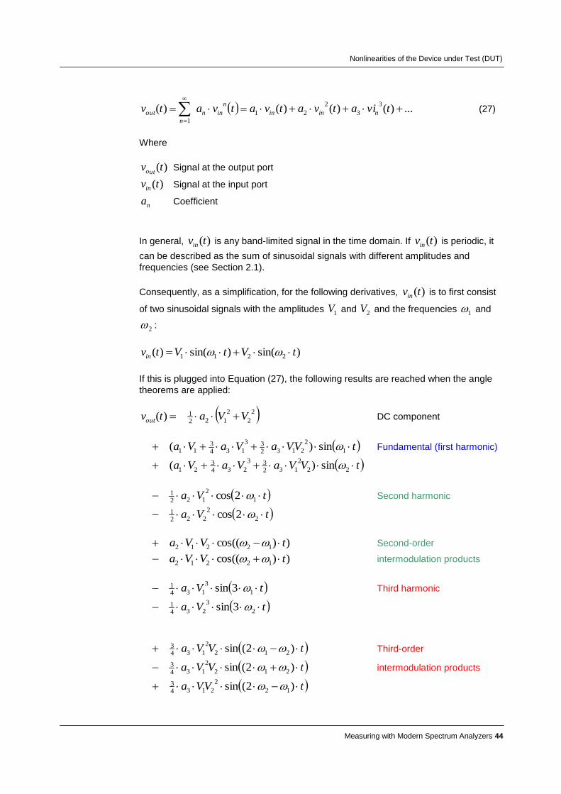
Nonlinearities of the Device under Test (DUT)
Measuring with Modern Spectrum Analyzers 44
...)()()()(3
3
2
21
1
tviatvatvatvatv ninin
n
inn
n
out (27)
Where
)(tvuto Signal at the output port
)(tvin Signal at the input port
na Coefficient
In general, )(tvin is any band-limited signal in the time domain. If )(tvin is periodic, it
can be described as the sum of sinusoidal signals with different amplitudes and
frequencies (see Section 2.1).
Consequently, as a simplification, for the following derivatives, )(tvin is to first consist
of two sinusoidal signals with the amplitudes 1V and 2V and the frequencies 1 and
2 :
)sin()sin()( 2211 tVtVtvin
If this is plugged into Equation (27), the following results are reached when the angle
theorems are applied:
2
2
2
1221)( VVatvout DC component
tVVaVaVa 1
2
213233
1343
11 sin)( Fundamental (first harmonic)
tVVaVaVa 22
2
13233
2343
21 sin)(
tVa 1
2
1221 2cos Second harmonic
tVa 2
2
2221 2cos
))cos(( 12212 tVVa Second-order
))cos(( 12212 tVVa intermodulation products
tVa 1
3
1341 3sin Third harmonic
tVa 2
3
2341 3sin
tVVa )2(sin 212
2
1343 Third-order
tVVa )2(sin 212
2
1343 intermodulation products
tVVa )2(sin 12
2
21343
Nonlinearities of the Device under Test (DUT)
Measuring with Modern Spectrum Analyzers 45
tVVa )2(sin 12
2
21343 (28)
The series is ended here after the third power.
This shows that other spectral components arise in addition to the fundamental:
a DC component and harmonics with a multiple of the fundamental frequency, plus
"intermodulation products" at the sums and differences of the fundamental frequencies
and harmonics.
The order number for these spectral lines is defined by the number of terms required
for the calculation. This calculation, for instance, requires three terms; consequently, it
is a third-order frequency:
2ω1 – ω2 = ω1 + ω1 – ω2
When the stimulus signal has only one sine wave ( 1V or 2V is equal to zero), there are
no intermodulation products.
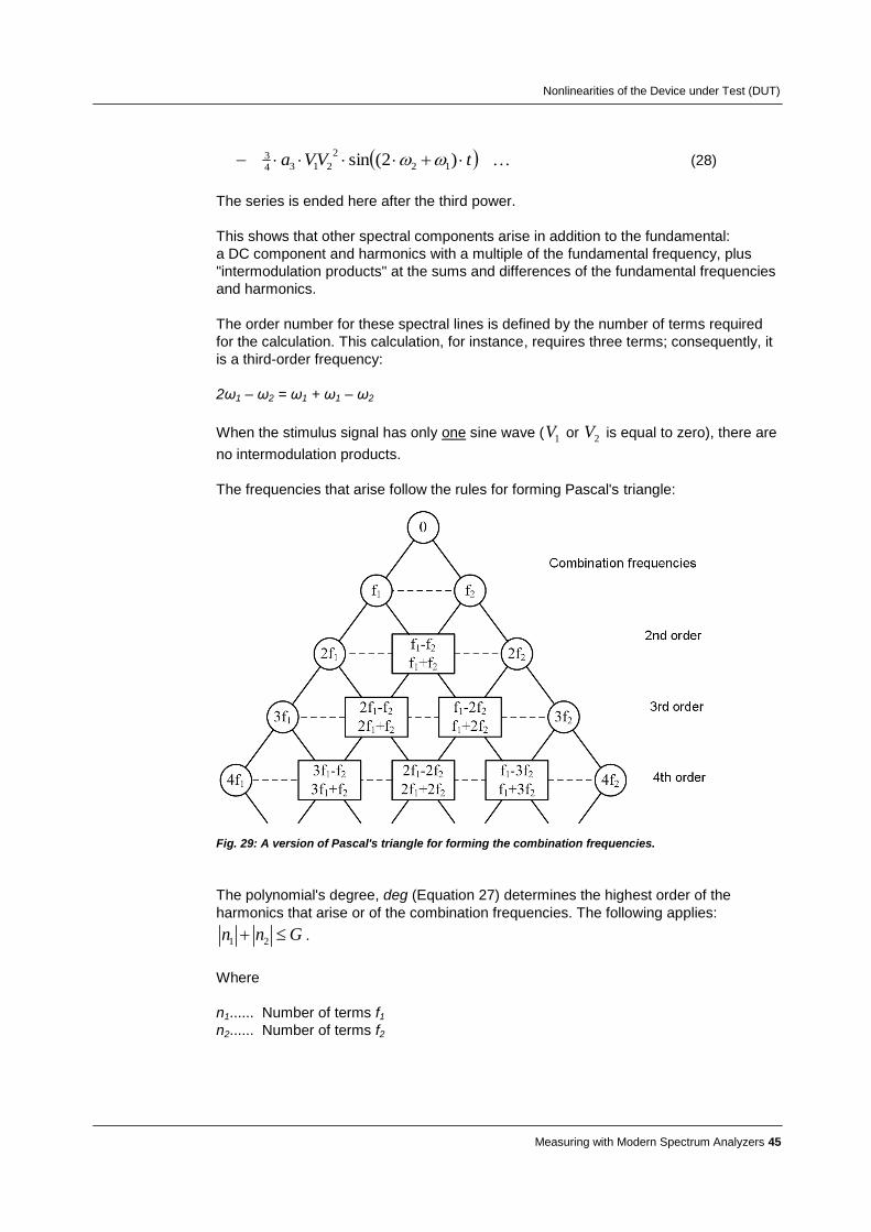
The frequencies that arise follow the rules for forming Pascal's triangle:
Fig. 29: A version of Pascal's triangle for forming the combination frequencies.
The polynomial's degree, deg (Equation 27) determines the highest order of the
harmonics that arise or of the combination frequencies. The following applies:
1 2n n G .
Where
n1...... Number of terms f1
n2...... Number of terms f2
Nonlinearities of the Device under Test (DUT)
Measuring with Modern Spectrum Analyzers 46
Equation (28) was derived for voltages. One obtains the output power, when V is
substituted with R
V 2
. The equation maintains its form.
When comparing the coefficients of the individual spectral components in Equation
(28), it becomes clear that the second-order intermodulation products are always 6 dB
higher than the second harmonic and that the third-order intermodulation products are
always 9.54 dB higher than the third harmonic. This is so because
)54.9)/log(20.6)log(20(43
41
21 dBbzwdB .
The third-order intermodulation products are particularly important. These
components are very pronounced, and some arise close to the fundamental
frequencies. In practice, filtering out nearby interference signals is difficult.
With wireless communications systems, for instance, the adjacent channel might
possibly be affected. For this reason, the various wireless communications standards
always include measurements that examine the extent of the TX stage's emissions into
the neighboring channel by measuring the adjacent channel leakage ratio (ACLR).
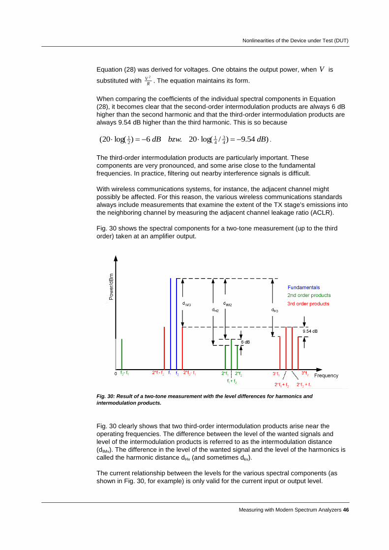
Fig. 30 shows the spectral components for a two-tone measurement (up to the third
order) taken at an amplifier output.
Fig. 30: Result of a two-tone measurement with the level differences for harmonics and
intermodulation products.
Fig. 30 clearly shows that two third-order intermodulation products arise near the
operating frequencies. The difference between the level of the wanted signals and
level of the intermodulation products is referred to as the intermodulation distance
(dIMν). The difference in the level of the wanted signal and the level of the harmonics is
called the harmonic distance dHν (and sometimes dkν).
The current relationship between the levels for the various spectral components (as
shown in Fig. 30, for example) is only valid for the current input or output level.
Nonlinearities of the Device under Test (DUT)
Measuring with Modern Spectrum Analyzers 47
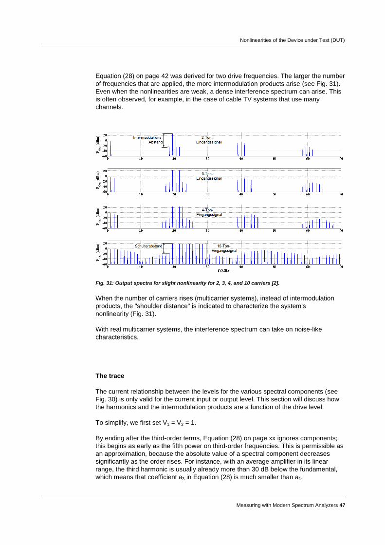
Equation (28) on page 42 was derived for two drive frequencies. The larger the number
of frequencies that are applied, the more intermodulation products arise (see Fig. 31).
Even when the nonlinearities are weak, a dense interference spectrum can arise. This
is often observed, for example, in the case of cable TV systems that use many
channels.
Fig. 31: Output spectra for slight nonlinearity for 2, 3, 4, and 10 carriers [2].
When the number of carriers rises (multicarrier systems), instead of intermodulation
products, the "shoulder distance" is indicated to characterize the system's
nonlinearity (Fig. 31).
With real multicarrier systems, the interference spectrum can take on noise-like
characteristics.
The trace
The current relationship between the levels for the various spectral components (see
Fig. 30) is only valid for the current input or output level. This section will discuss how
the harmonics and the intermodulation products are a function of the drive level.
To simplify, we first set V1 = V2 = 1.
By ending after the third-order terms, Equation (28) on page xx ignores components;
this begins as early as the fifth power on third-order frequencies. This is permissible as
an approximation, because the absolute value of a spectral component decreases
significantly as the order rises. For instance, with an average amplifier in its linear
range, the third harmonic is usually already more than 30 dB below the fundamental,
which means that coefficient a3 in Equation (28) is much smaller than a1.
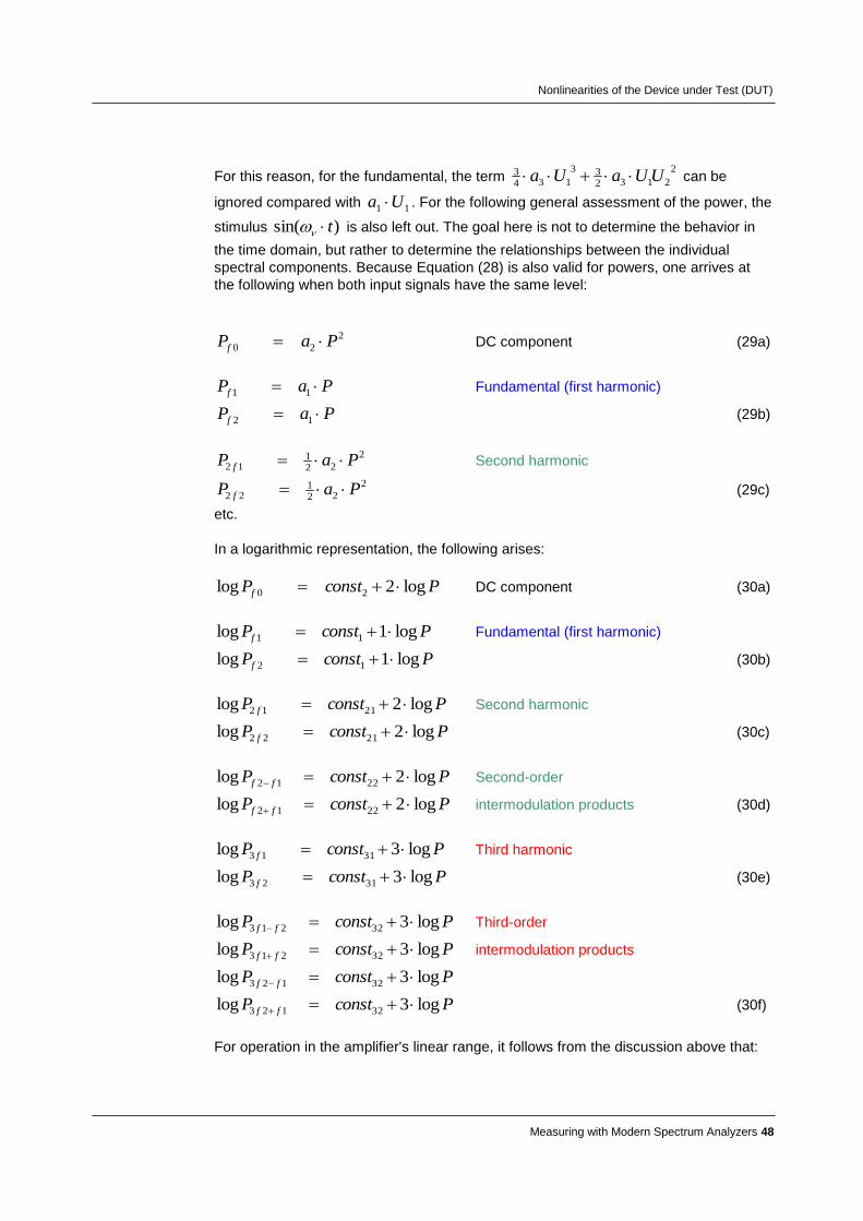
Nonlinearities of the Device under Test (DUT)
Measuring with Modern Spectrum Analyzers 48
For this reason, for the fundamental, the term 2
213233
1343 UUaUa can be
ignored compared with 11 Ua . For the following general assessment of the power, the
stimulus )sin( t is also left out. The goal here is not to determine the behavior in
the time domain, but rather to determine the relationships between the individual
spectral components. Because Equation (28) is also valid for powers, one arrives at
the following when both input signals have the same level:
2
20 PaPf DC component (29a)
PaPf 11 Fundamental (first harmonic)
PaPf 12 (29b)
2
221
12 PaP f Second harmonic
2
221
22 PaP f (29c)
etc.
In a logarithmic representation, the following arises:
PconstPf log2log 20 DC component (30a)
PconstPf log1log 11 Fundamental (first harmonic)
PconstPf log1log 12 (30b)
PconstP f log2log 2112 Second harmonic
PconstP f log2log 2122 (30c)
PconstP ff log2log 2212 Second-order
PconstP ff log2log 2212 intermodulation products (30d)
PconstP f log3log 3113 Third harmonic
PconstP f log3log 3123 (30e)
PconstP ff log3log 32213 Third-order
PconstP ff log3log 32213 intermodulation products
PconstP ff log3log 32123
PconstP ff log3log 32123 (30f)
For operation in the amplifier's linear range, it follows from the discussion above that:
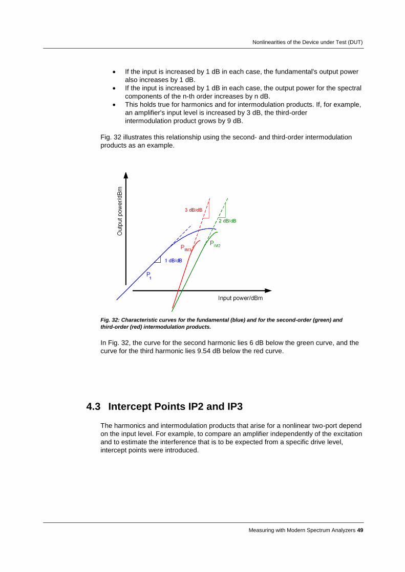
Nonlinearities of the Device under Test (DUT)
Measuring with Modern Spectrum Analyzers 49
If the input is increased by 1 dB in each case, the fundamental's output power
also increases by 1 dB.
If the input is increased by 1 dB in each case, the output power for the spectral
components of the n-th order increases by n dB.
This holds true for harmonics and for intermodulation products. If, for example,
an amplifier's input level is increased by 3 dB, the third-order
intermodulation product grows by 9 dB.
Fig. 32 illustrates this relationship using the second- and third-order intermodulation
products as an example.
Fig. 32: Characteristic curves for the fundamental (blue) and for the second-order (green) and
third-order (red) intermodulation products.
In Fig. 32, the curve for the second harmonic lies 6 dB below the green curve, and the
curve for the third harmonic lies 9.54 dB below the red curve.
4.3 Intercept Points IP2 and IP3
The harmonics and intermodulation products that arise for a nonlinear two-port depend
on the input level. For example, to compare an amplifier independently of the excitation
and to estimate the interference that is to be expected from a specific drive level,
intercept points were introduced.
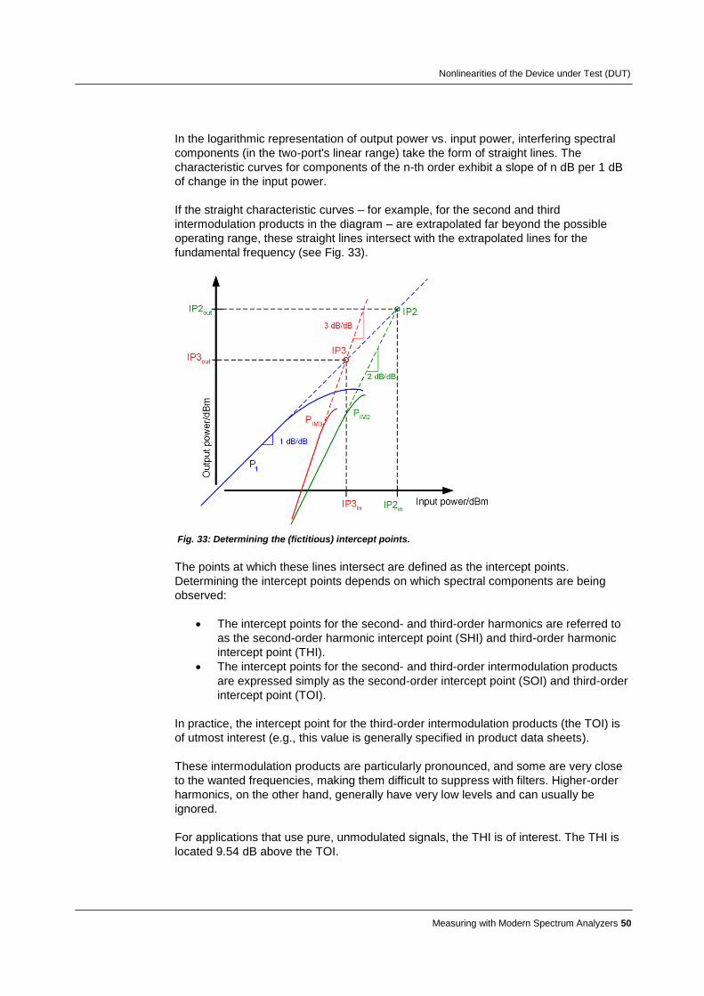
Nonlinearities of the Device under Test (DUT)
Measuring with Modern Spectrum Analyzers 50
In the logarithmic representation of output power vs. input power, interfering spectral
components (in the two-port's linear range) take the form of straight lines. The
characteristic curves for components of the n-th order exhibit a slope of n dB per 1 dB
of change in the input power.
If the straight characteristic curves – for example, for the second and third
intermodulation products in the diagram – are extrapolated far beyond the possible
operating range, these straight lines intersect with the extrapolated lines for the
fundamental frequency (see Fig. 33).
Fig. 33: Determining the (fictitious) intercept points.
The points at which these lines intersect are defined as the intercept points.
Determining the intercept points depends on which spectral components are being
observed:
The intercept points for the second- and third-order harmonics are referred to
as the second-order harmonic intercept point (SHI) and third-order harmonic
intercept point (THI).
The intercept points for the second- and third-order intermodulation products
are expressed simply as the second-order intercept point (SOI) and third-order
intercept point (TOI).
In practice, the intercept point for the third-order intermodulation products (the TOI) is
of utmost interest (e.g., this value is generally specified in product data sheets).
These intermodulation products are particularly pronounced, and some are very close
to the wanted frequencies, making them difficult to suppress with filters. Higher-order
harmonics, on the other hand, generally have very low levels and can usually be
ignored.
For applications that use pure, unmodulated signals, the THI is of interest. The THI is
located 9.54 dB above the TOI.
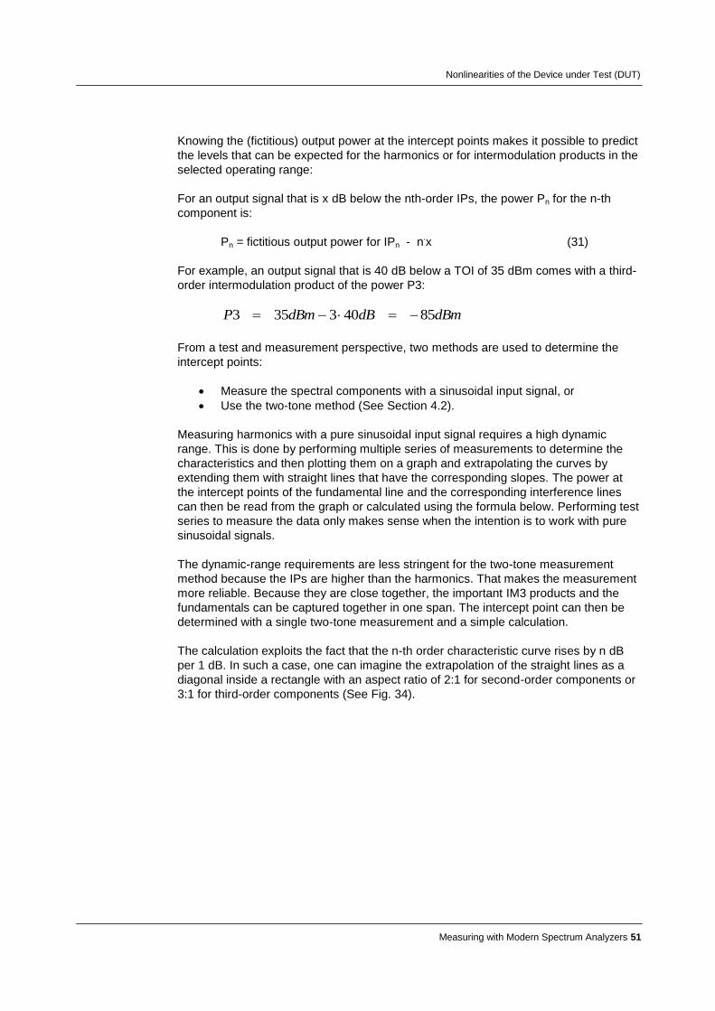
Nonlinearities of the Device under Test (DUT)
Measuring with Modern Spectrum Analyzers 51
Knowing the (fictitious) output power at the intercept points makes it possible to predict
the levels that can be expected for the harmonics or for intermodulation products in the
selected operating range:
For an output signal that is x dB below the nth-order IPs, the power Pn for the n-th
component is:
Pn = fictitious output power for IPn - n.x (31)
For example, an output signal that is 40 dB below a TOI of 35 dBm comes with a third-
order intermodulation product of the power P3:
dBmdBdBmP 85403353
From a test and measurement perspective, two methods are used to determine the
intercept points:
Measure the spectral components with a sinusoidal input signal, or
Use the two-tone method (See Section 4.2).
Measuring harmonics with a pure sinusoidal input signal requires a high dynamic
range. This is done by performing multiple series of measurements to determine the
characteristics and then plotting them on a graph and extrapolating the curves by
extending them with straight lines that have the corresponding slopes. The power at
the intercept points of the fundamental line and the corresponding interference lines
can then be read from the graph or calculated using the formula below. Performing test
series to measure the data only makes sense when the intention is to work with pure
sinusoidal signals.
The dynamic-range requirements are less stringent for the two-tone measurement
method because the IPs are higher than the harmonics. That makes the measurement
more reliable. Because they are close together, the important IM3 products and the
fundamentals can be captured together in one span. The intercept point can then be
determined with a single two-tone measurement and a simple calculation.
The calculation exploits the fact that the n-th order characteristic curve rises by n dB
per 1 dB. In such a case, one can imagine the extrapolation of the straight lines as a
diagonal inside a rectangle with an aspect ratio of 2:1 for second-order components or
3:1 for third-order components (See Fig. 34).
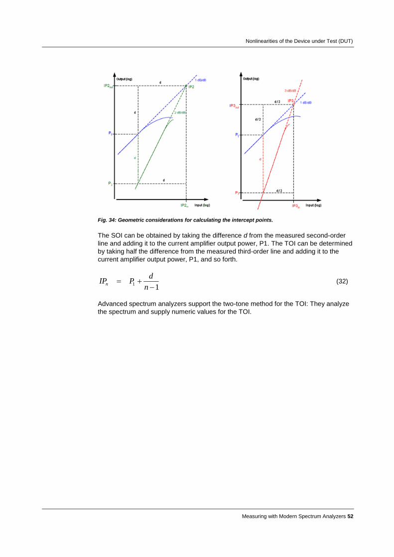
Nonlinearities of the Device under Test (DUT)
Measuring with Modern Spectrum Analyzers 52
Fig. 34: Geometric considerations for calculating the intercept points.
The SOI can be obtained by taking the difference d from the measured second-order
line and adding it to the current amplifier output power, P1. The TOI can be determined
by taking half the difference from the measured third-order line and adding it to the
current amplifier output power, P1, and so forth.
11
n
dPIPn (32)
Advanced spectrum analyzers support the two-tone method for the TOI: They analyze
the spectrum and supply numeric values for the TOI.
Crest Factor and Complementary Cumulative Distribution Function (CCDF)
Measuring with Modern Spectrum Analyzers 53
5 Crest Factor and Complementary Cumulative Distribution Function (CCDF)
This chapter covers RF signals that have a high crest factor, i.e., signals with peaks
high above the RMS value:
RMS
PeakCF
Those types of signals arise primarily when advanced digital modulation schemes such
as n-Phase Shift Keying (nPSK), Quadrature Modulation (QAM), Code Division
Multiple Access (CDMA), or Orthogonal Frequency Division Multiplex (OFDM) are
employed. Signals with a high crest factor arise in cellular networks, in digital
television, and in many broadband transmission systems. In the time domain, as in the
allocated frequency range, these signals are similar to thermal noise at first glance.
An RF signal's crest factor can refer to the overall signal or only to the modulated
envelope. The discussion below is based exclusively on the latter view (modulated
envelope). Consequently, the crest factor is the same for generation in the baseband
as it is for the operating frequency: The crest factor for an unmodulated RF signal is CF
= 0. If the first perspective had been taken, its crest factor would have been CF =
3.01 dB (sine-wave carrier).
Indicating the crest factor in dB makes sense in that only one value is required to
examine both the voltage and power levels.
The crest factor focuses the view on the signal peaks. This is important for configuring
a system to have the proper amount of electrical strength.
In practice, however, the probability of signal peaks arising is low. The probability of
what the level might be at a given point in time is determined using the complementary
cumulative distribution function (CCDF). Advanced spectrum analyzers offer this
measurement function (see Fig. 35 page 54).
The yellow line shows the probability that certain levels will be exceeded. This line is
typical in that a relative flat beginning is followed by a rapidly increasing drop. This
means that the larger the peaks, the lower the probability that they will arise. A
theoretical maximum level can be calculated.
For reference purposes, the red line shows the CCDF for white noise. Unlike the CCDF
for the 3GPP-FDD signal, in this case, there is no rapid decrease of that kind and no
maximum level. Theoretically, over the course of an infinite acquisition time (AQT), an
infinitely high level would arise at least once.
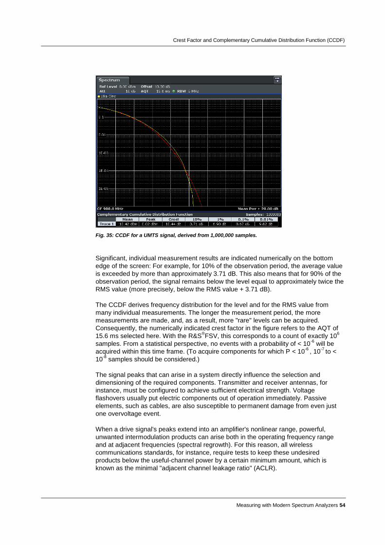
Crest Factor and Complementary Cumulative Distribution Function (CCDF)
Measuring with Modern Spectrum Analyzers 54
Fig. 35: CCDF for a UMTS signal, derived from 1,000,000 samples.
Significant, individual measurement results are indicated numerically on the bottom
edge of the screen: For example, for 10% of the observation period, the average value
is exceeded by more than approximately 3.71 dB. This also means that for 90% of the
observation period, the signal remains below the level equal to approximately twice the
RMS value (more precisely, below the RMS value + 3.71 dB).
The CCDF derives frequency distribution for the level and for the RMS value from
many individual measurements. The longer the measurement period, the more
measurements are made, and, as a result, more "rare" levels can be acquired.
Consequently, the numerically indicated crest factor in the figure refers to the AQT of
15.6 ms selected here. With the R&S®FSV, this corresponds to a count of exactly 10
6
samples. From a statistical perspective, no events with a probability of < 10-6
will be
acquired within this time frame. (To acquire components for which P < 10-6
, 10-7
to <
10-8
samples should be considered.)
The signal peaks that can arise in a system directly influence the selection and
dimensioning of the required components. Transmitter and receiver antennas, for
instance, must be configured to achieve sufficient electrical strength. Voltage
flashovers usually put electric components out of operation immediately. Passive
elements, such as cables, are also susceptible to permanent damage from even just
one overvoltage event.
When a drive signal's peaks extend into an amplifier's nonlinear range, powerful,
unwanted intermodulation products can arise both in the operating frequency range
and at adjacent frequencies (spectral regrowth). For this reason, all wireless
communications standards, for instance, require tests to keep these undesired
products below the useful-channel power by a certain minimum amount, which is
known as the minimal "adjacent channel leakage ratio" (ACLR).
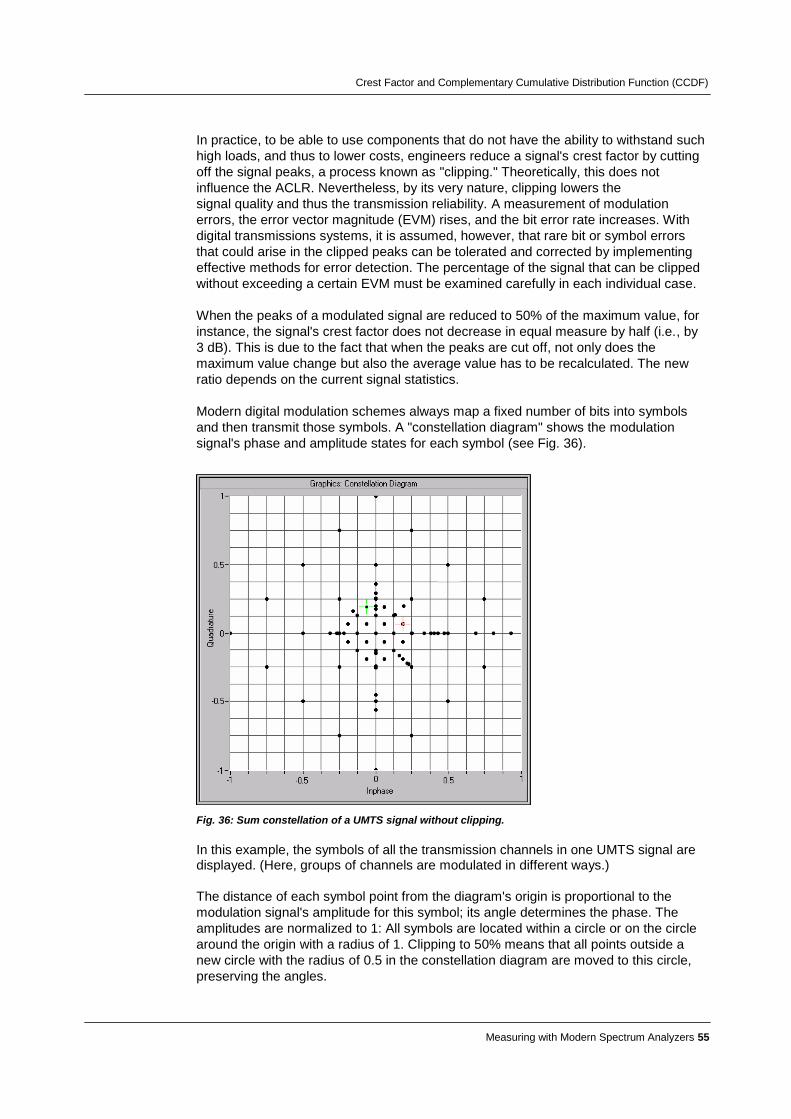
Crest Factor and Complementary Cumulative Distribution Function (CCDF)
Measuring with Modern Spectrum Analyzers 55
In practice, to be able to use components that do not have the ability to withstand such
high loads, and thus to lower costs, engineers reduce a signal's crest factor by cutting
off the signal peaks, a process known as "clipping." Theoretically, this does not
influence the ACLR. Nevertheless, by its very nature, clipping lowers the
signal quality and thus the transmission reliability. A measurement of modulation
errors, the error vector magnitude (EVM) rises, and the bit error rate increases. With
digital transmissions systems, it is assumed, however, that rare bit or symbol errors
that could arise in the clipped peaks can be tolerated and corrected by implementing
effective methods for error detection. The percentage of the signal that can be clipped
without exceeding a certain EVM must be examined carefully in each individual case.
When the peaks of a modulated signal are reduced to 50% of the maximum value, for
instance, the signal's crest factor does not decrease in equal measure by half (i.e., by
3 dB). This is due to the fact that when the peaks are cut off, not only does the
maximum value change but also the average value has to be recalculated. The new
ratio depends on the current signal statistics.
Modern digital modulation schemes always map a fixed number of bits into symbols
and then transmit those symbols. A "constellation diagram" shows the modulation
signal's phase and amplitude states for each symbol (see Fig. 36).
Fig. 36: Sum constellation of a UMTS signal without clipping.
In this example, the symbols of all the transmission channels in one UMTS signal are displayed. (Here, groups of channels are modulated in different ways.)
The distance of each symbol point from the diagram's origin is proportional to the
modulation signal's amplitude for this symbol; its angle determines the phase. The
amplitudes are normalized to 1: All symbols are located within a circle or on the circle
around the origin with a radius of 1. Clipping to 50% means that all points outside a
new circle with the radius of 0.5 in the constellation diagram are moved to this circle,
preserving the angles.
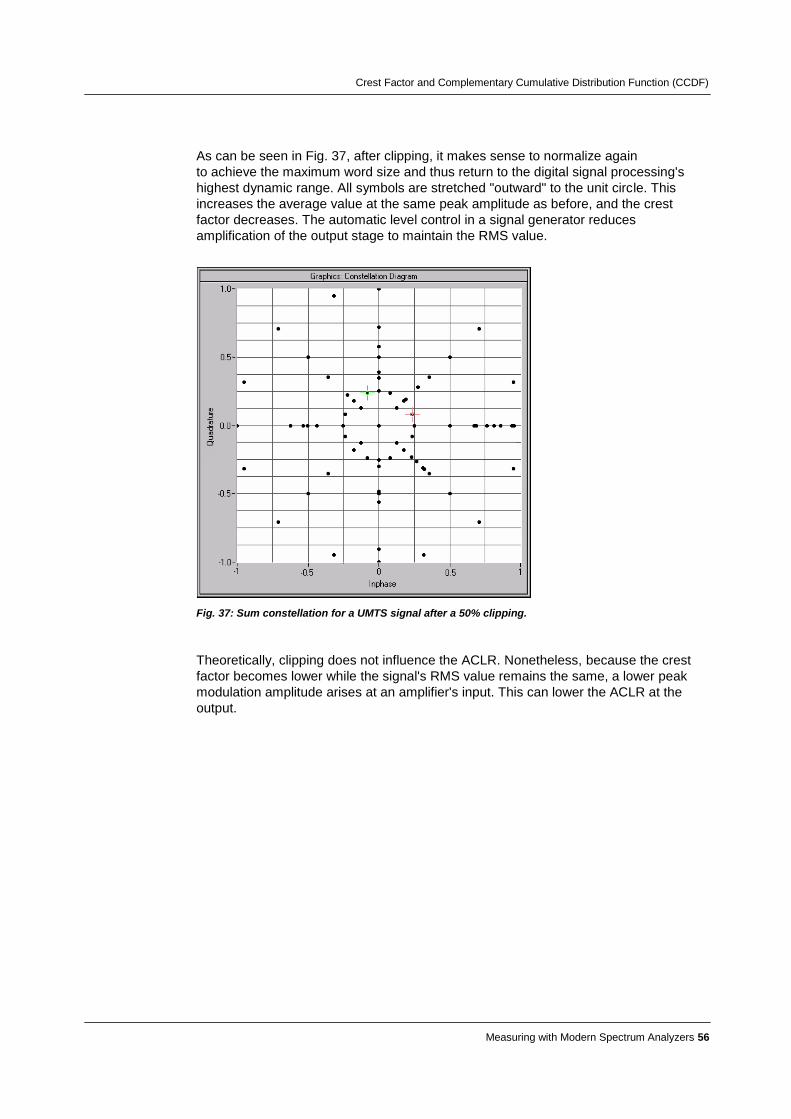
Crest Factor and Complementary Cumulative Distribution Function (CCDF)
Measuring with Modern Spectrum Analyzers 56
As can be seen in Fig. 37, after clipping, it makes sense to normalize again
to achieve the maximum word size and thus return to the digital signal processing's
highest dynamic range. All symbols are stretched "outward" to the unit circle. This
increases the average value at the same peak amplitude as before, and the crest
factor decreases. The automatic level control in a signal generator reduces
amplification of the output stage to maintain the RMS value.
Fig. 37: Sum constellation for a UMTS signal after a 50% clipping.
Theoretically, clipping does not influence the ACLR. Nonetheless, because the crest
factor becomes lower while the signal's RMS value remains the same, a lower peak
modulation amplitude arises at an amplifier's input. This can lower the ACLR at the
output.
Phase Noise
Measuring with Modern Spectrum Analyzers 57
6 Phase Noise The information provided in this chapter has been taken largely from the application
note "Phase Noise Measurements with Spectrum Analyzers of the FSE Family" by
Josef Wolf [6].
Phase noise describes a frequency's short-term stability, which makes it one of the
signal source's important characteristics (along with other characteristics such as the
frequency range and long-term stability, power, and spectral purity).
An oscillator's phase noise is the reason why the oscillator not only appears as a line in
the spectrum, but also appears continuously at frequencies below and above the target
frequency – although the probability decreases sharply as the distance increases.
Phase noise, or rather the measurement of the phase noise of oscillators and
synthesizers, is very important, particularly in wireless transmission systems. With
receivers, the conversion oscillators' phase noise reduces sensitivity in adjacent
channels when a strong input signal is present. With transmitters, the oscillator's phase
noise is, together with the modulator characteristics, responsible for the undesired
power emitted in the adjacent channels.
Mathematically, the output signal tu of an ideal oscillator can be described as
follows:
tfVtv 00 2sin Where
0V Signal amplitude
0f Signal frequency and
tf02 Signal phase
With real signals, both the signal's amplitude and its phase are subject to variation:
)(2sin))(( 00 ttftVtv Where
)(t The signal's amplitude variation and
)(t The signal's (phase variation or) phase noise
When working with the term )(t , it is necessary to differentiate between two types:
Deterministic phase variation due, for instance, to AC hum or to insufficient
suppression of other frequencies during signal processing. These fluctuations
appear as discrete lines of interference.
Random phase variation caused by thermal, shot, or flicker noise in the active
elements of oscillators.

Phase Noise
Measuring with Modern Spectrum Analyzers 58
One measure of phase noise is the noise power density with reference to 1 Hz of
bandwidth:
Hz
rad
HzfS
rms22
1)(
In practice, single-sideband (SSB) phase noise L is usually used to describe an
oscillator's phase-noise characteristics. L is defined as the ratio of the noise power in
one sideband (measured over a bandwidth of 1 Hz) SSBP to the signal power CarrierP at
a frequency offset mf from the carrier).
Carrier
SSBm
P
HzPfL
1)(
If the modulation sidebands are very small due to noise, e.g., if phase deviation is much smaller than 1 rad, the SSB phase noise can be derived from the noise power density:
)(2
1)( fSfL
The SSB phase noise is commonly specified on a logarithmic scale [dBc / Hz]:
))((log10)( mmc fLfL
Measurement methods
The simplest and fastest way to determine an oscillator's phase noise is to perform a
direct measurement using a spectrum analyzer.
For this measurement, these conditions must be met:
The frequency drift of the device under test (DUT) must be small relative to the
spectrum-analyzer sweep time. Otherwise, the signal-to-noise ratio will not be
calculated correctly. The
synthesizers commonly used in radiocommunications always fulfill this condition.
The DUT can be locked to a reference of sufficient stability, or the DUT and
analyzer can be synchronized directly.
The spectrum analyzer's phase noise and AM noise must be low enough to ensure
that the focus is on the DUT's phase noise and that it is not the spectrum
analyzer's characteristics that are measured. The analyzer always provides the
sum of the DUT's AM noise and phase noise and its own phase noise and AM
noise.
The DUT's amplitude noise must be significantly lower than the phase noise. This
requirement is certainly met in the range close to the carrier frequency.
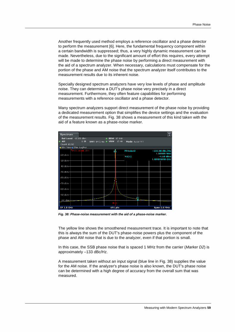
Phase Noise
Measuring with Modern Spectrum Analyzers 59
Another frequently used method employs a reference oscillator and a phase detector
to perform the measurement [6]. Here, the fundamental frequency component within
a certain bandwidth is suppressed; thus, a very highly dynamic measurement can be
made. Nevertheless, due to the significant amount of effort this requires, every attempt
will be made to determine the phase noise by performing a direct measurement with
the aid of a spectrum analyzer. When necessary, calculations must compensate for the
portion of the phase and AM noise that the spectrum analyzer itself contributes to the
measurement results due to its inherent noise.
Specially designed spectrum analyzers have very low levels of phase and amplitude
noise. They can determine a DUT's phase noise very precisely in a direct
measurement. Furthermore, they often feature capabilities for performing
measurements with a reference oscillator and a phase detector.
Many spectrum analyzers support direct measurement of the phase noise by providing
a dedicated measurement option that simplifies the device settings and the evaluation
of the measurement results. Fig. 38 shows a measurement of this kind taken with the
aid of a feature known as a phase-noise marker.
Fig. 38: Phase-noise measurement with the aid of a phase-noise marker.
The yellow line shows the smoothened measurement trace. It is important to note that
this is always the sum of the DUT's phase-noise powers plus the component of the
phase and AM noise that is due to the analyzer, even if that portion is small.
In this case, the SSB phase noise that is spaced 1 MHz from the carrier (Marker D2) is
approximately –133 dBc/Hz.
A measurement taken without an input signal (blue line in Fig. 38) supplies the value
for the AM noise. If the analyzer's phase noise is also known, the DUT's phase noise
can be determined with a high degree of accuracy from the overall sum that was
measured.
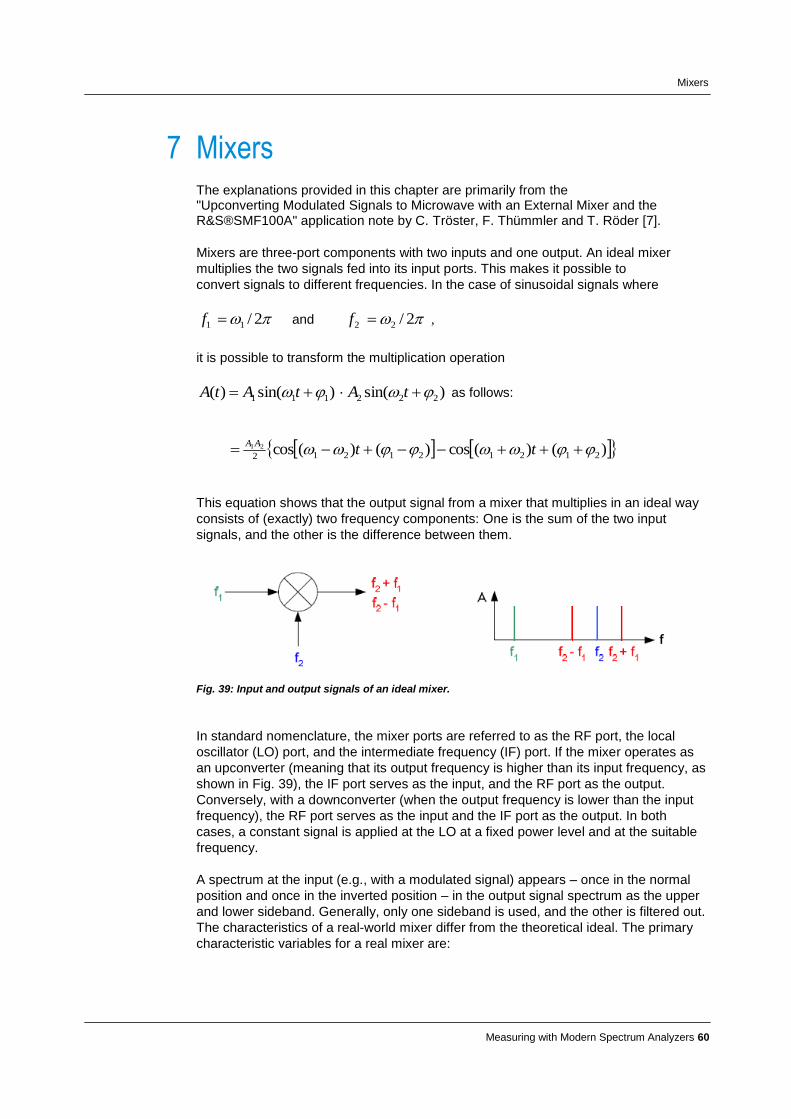
Mixers
Measuring with Modern Spectrum Analyzers 60
7 Mixers The explanations provided in this chapter are primarily from the "Upconverting Modulated Signals to Microwave with an External Mixer and the R&S®SMF100A" application note by C. Tröster, F. Thümmler and T. Röder [7].
Mixers are three-port components with two inputs and one output. An ideal mixer
multiplies the two signals fed into its input ports. This makes it possible to
convert signals to different frequencies. In the case of sinusoidal signals where
2/11 f and 2/22 f ,
it is possible to transform the multiplication operation
)sin()sin()( 222111 tAtAtA as follows:
)()(cos)()(cos 21212121221 tt
AA
This equation shows that the output signal from a mixer that multiplies in an ideal way
consists of (exactly) two frequency components: One is the sum of the two input
signals, and the other is the difference between them.
Fig. 39: Input and output signals of an ideal mixer.
In standard nomenclature, the mixer ports are referred to as the RF port, the local
oscillator (LO) port, and the intermediate frequency (IF) port. If the mixer operates as
an upconverter (meaning that its output frequency is higher than its input frequency, as
shown in Fig. 39), the IF port serves as the input, and the RF port as the output.
Conversely, with a downconverter (when the output frequency is lower than the input
frequency), the RF port serves as the input and the IF port as the output. In both
cases, a constant signal is applied at the LO at a fixed power level and at the suitable
frequency.
A spectrum at the input (e.g., with a modulated signal) appears – once in the normal
position and once in the inverted position – in the output signal spectrum as the upper
and lower sideband. Generally, only one sideband is used, and the other is filtered out.
The characteristics of a real-world mixer differ from the theoretical ideal. The primary
characteristic variables for a real mixer are:
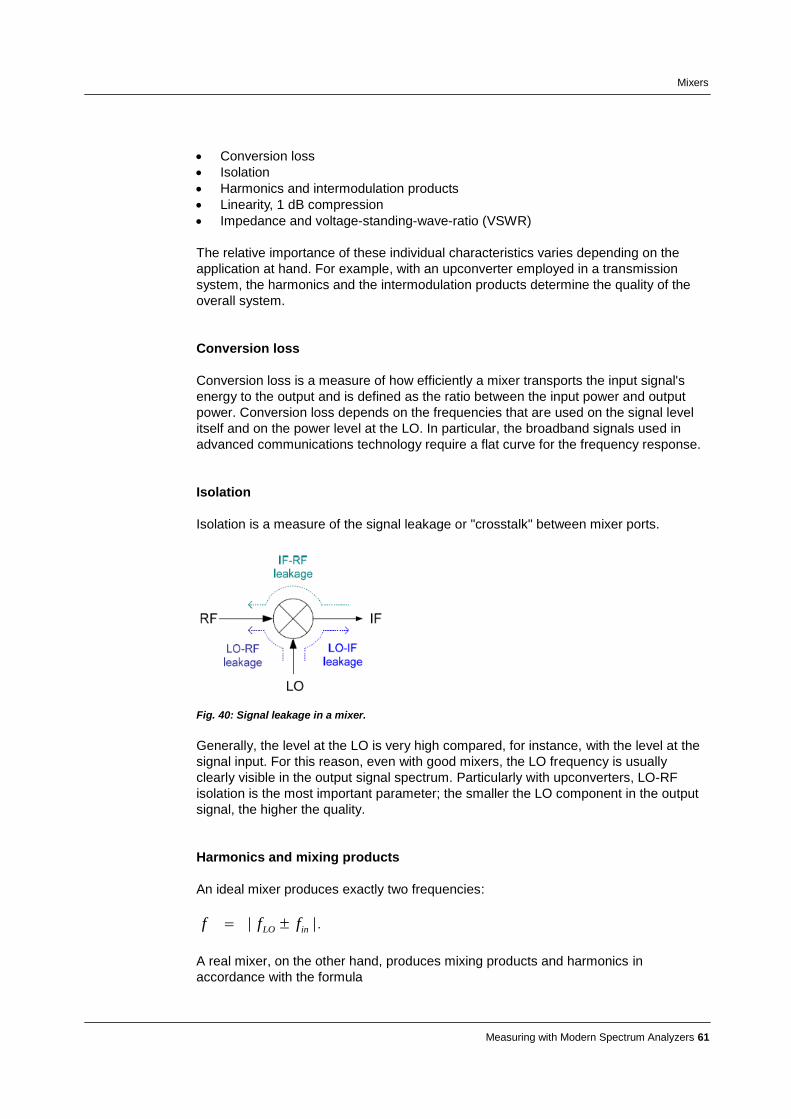
Mixers
Measuring with Modern Spectrum Analyzers 61
Conversion loss
Isolation
Harmonics and intermodulation products
Linearity, 1 dB compression
Impedance and voltage-standing-wave-ratio (VSWR)
The relative importance of these individual characteristics varies depending on the
application at hand. For example, with an upconverter employed in a transmission
system, the harmonics and the intermodulation products determine the quality of the
overall system.
Conversion loss
Conversion loss is a measure of how efficiently a mixer transports the input signal's
energy to the output and is defined as the ratio between the input power and output
power. Conversion loss depends on the frequencies that are used on the signal level
itself and on the power level at the LO. In particular, the broadband signals used in
advanced communications technology require a flat curve for the frequency response.
Isolation
Isolation is a measure of the signal leakage or "crosstalk" between mixer ports.
Fig. 40: Signal leakage in a mixer.
Generally, the level at the LO is very high compared, for instance, with the level at the
signal input. For this reason, even with good mixers, the LO frequency is usually
clearly visible in the output signal spectrum. Particularly with upconverters, LO-RF
isolation is the most important parameter; the smaller the LO component in the output
signal, the higher the quality.
Harmonics and mixing products
An ideal mixer produces exactly two frequencies:
|| inLO fff .
A real mixer, on the other hand, produces mixing products and harmonics in
accordance with the formula
Mixers
Measuring with Modern Spectrum Analyzers 62
||, inLO Fff
where and are integers (...,-2, -1, 0, 1, 2,...). For example, the lower sideband
arises with the values = 1 and = -1, and the upper sideband arises with the
value = = 1. The individual components differ inherently in amplitude. The lower
and upper sidebands are the strongest mixer products; all other mixing products have
lower amplitudes. Nevertheless, those other products can still result in a relatively large
power level in the output spectrum. That is particularly true for the LO harmonics.
The higher LOf is, the higher the frequencies of the LO harmonics. Because the
system is band-limited at the mixer output, these harmonics do not appear in their full
strength.
Linearity
With mixers, as with amplifiers, the power level at the output only remains proportional
to the level at the input within a certain range. At a certain input power, the output
signal begins to reach saturation. The 1 dB compression point is defined as the input
power at which the output power sinks to 1 dB below the ideal linear characteristic
curve.
The difference in amplitude between the noise floor and the 1 dB compression point is
referred to as the (linear) dynamic range.
Intermodulation products
Like amplifiers, mixers do not offer ideal linearity, even when they are driven within the
range below the 1 dB compression point. For this reason, when two or more signals
are applied simultaneously at the input, a whole series of intermodulation products –
most of which are interference – arise at the output (in addition to the harmonics and
mixing products with the LO signal).
When there are two signals with the frequencies 1f and 2f at the input of a
component that is not ideally linear, the output contains spectral components at
the frequencies
|| 21, fmfnf mn
where m and n are integers (...,-2, -1, 0, 1, 2,...). The most problematic type are the
third-order intermodulation products at the frequencies 212 ff and 122 ff ,
because they are close to the fundamental frequency.
The same principles and measurement procedures apply here as do those for
amplifiers.

Measuring with Modern Spectrum Analyzers 63
References
Measuring with Modern Spectrum Analyzers 64
8 References
[1] Rauscher, Christoph. Fundamentals of Spectrum Analysis. Munich, Germany:
Rohde & Schwarz®, 5th Edition, 2011.
[2] Leitinger, Erik; Magerl, Gottfried; Gadringer,, Michael.Radio Frequency
Equipment Lab, Spectral Analysis, Script for Lab Exercise
Technical Universities of Graz and Vienna, Austria, 2011.
[3] Minihold, Roland. Measuring the Nonlinearities of RF Amplifiers Using Signal
Generators and a Spectrum Analyzer, Application Note 1MA71. Munich,
Germany: Rohde & Schwarz®, 2006.
[4] Simon, Michael. Interaction of Intermodulation Products between DUT and
Spectrum Analyzer, White Paper. Munich, Germany, Rohde & Schwarz®,
2012.
[5] Kaes, Bernhard. The Crest Factor in DVB-T (OFDM) Transmitter Systems and
its Influence on the Dimensioning of Power Components, Application Note
7TS02_2E.Munich, Germany: Rohde & Schwarz®, 2007
[6] Wolf, Josef. Phase Noise Measurements with Spectrum Analyzers of the FSE
Family, Application Note 1EPAN 16E. Munich, Germany: Rohde & Schwarz®,
1995.
[7] Tröster, C; Thümmler, F; Röder, T. Upconverting Modulated Signals to Microwave with an External Mixer and the R&S®SMF100A, Application Note 1GP65. Munich, Germany: Rohde & Schwarz
®, 2008.
About Rohde & Schwarz
Rohde & Schwarz is an independent group
of companies specializing in electronics. It is
a leading supplier of solutions in the fields of
test and measurement, broadcasting,
radiomonitoring, and radiolocation, as well
as secure communications. Established
more than 75 years ago, Rohde & Schwarz
has a global presence and a dedicated
service network in more than 70 countries.
Company headquarters are in Munich,
Germany.
Regional contact
Europe, Africa, Middle East
+49 89 4129 12345
[email protected] North America
1-888-TEST-RSA (1-888-837-8772)
[email protected] Latin America
+1-410-910-7988
[email protected] Asia/Pacific
+65 65 13 04 88
[email protected] China
+86-800-810-8228 /+86-400-650-5896