SPECIFICATIONd114hh0cykhyb0.cloudfront.net/pdfs/spmwht5225d5waq0s0.pdf · samsung led page1/31 rev:...
31
SAMSUNG LED PAGE 1/31 Rev: SAMSUNG LED CO., LTD. 314. MAETAN 3-DONG, YEONGTONG-GU, SUWON-SI,GYEONGGI-DO,KOREA,443-743 ISSUE NO : 2011. 10. 19 5630 CRI80+ WHITE LED Q0 RANK DATE OF ISSUE : SPECIFICATION MODEL : SPMWHT5225D5WAQ0S0 CUSTOMER : CHECKED APPROVED SAMSUNG LED DRAWN CHECKED APPROVED SALES QUALITY Approved rank : VF(A1, A2, A3, A4, A5) CIE(Q1, Q2, Q3, Q4, Q5, Q6, Q7, Q8) IV(S1, S2, S3)
Transcript of SPECIFICATIONd114hh0cykhyb0.cloudfront.net/pdfs/spmwht5225d5waq0s0.pdf · samsung led page1/31 rev:...

SAMSUNG LED PAGE 1/31
Rev:
SAMSUNG LED CO., LTD.
314. MAETAN 3-DONG, YEONGTONG-GU,
SUWON-SI,GYEONGGI-DO,KOREA,443-743
ISSUE NO :
2011. 10. 19
5630 CRI80+ WHITE LED Q0 RANK
DATE OF ISSUE :
SPECIF ICAT IONMODEL : SPMWHT5225D5WAQ0S0
CUSTOMER :
CHECKED APPROVED
SAMSUNG LED
DRAWNCHECKED
APPROVEDSALES QUALITY
Approved rank :
VF(A1, A2, A3, A4, A5)
CIE(Q1, Q2, Q3, Q4, Q5, Q6, Q7, Q8)
IV(S1, S2, S3)

SAMSUNG LED PAGE 2/31
Contents
1. Product Outline ---------------------------------------------- 3
2. Absolute Maximum Rating ------------------------------- 3
3. Characteristics ---------------------------------------------- 3
4. Chromaticity Diagram ------------------------------------- 5
5. Typical Characteristic Graph ---------------------------- 6
6. Outline Drawing & Dimension -------------------------- 7
7. Reliability Test Items & Conditions ------------------- 8
8. Solder Conditions -------------------------------------------- 9
9. Taping Dimension -------------------------------------------- 10
10. Label Structure ----------------------------------------------- 11
11. Lot Number ---------------------------------------------------- 11
12. Reel Packing Structure ------------------------------------ 12
13. Aluminum Vinyl Bag ----------------------------------- 13
14. Precaution For Use ----------------------------------------- 14
15. Hazard Substance Analysis (SGS) ------------------ 16
16. Hazard Substance Analysis (SVHC) ------------------ 23
17. Revision History ---------------------------------------------- 31
SAMSUNG LED PAGE 3/31
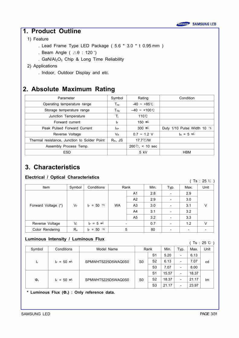
1. Product Outline1) Feature
. Lead Frame Type LED Package ( 5.6 * 3.0 * t 0.95 mm )
. Beam Angle ( △θ : 120 ˚)
. GaN/Al2O3 Chip & Long Time Reliability
2) Applications
. Indoor, Outdoor Display and etc.
2. Absolute Maximum Rating
Parameter Symbol Rating Condition
Operating temperature range Top -40 ~ +85℃Storage temperature range Tstg –40 ~ +100℃
Junction Temperature Tj 110℃Forward current IF 150 ㎃
Peak Pulsed Forward Current IFP 300 ㎃ Duty 1/10 Pulse Width 10 ㎳Reverse Voltage VR 0.7 ~ 1.2 V IR = 5 ㎃
Thermal resistance, Junction to Solder Point Rth, JS 17.7℃/W
Assembly Process Temp. 260℃, < 10 sec
ESD 5 kV HBM
3. Characteristics
Electrical / Optical Characteristics
Item Symbol Conditions Rank Min. Typ. Max. Unit
Forward Voltage (*) VF IF = 50 ㎃ WA
A1 2.8 - 2.9
V
A2 2.9 - 3.0
A3 3.0 - 3.1
A4 3.1 - 3.2
A5 3.2 - 3.3
Reverse Voltage Vr IF = 5 ㎃ - 0.7 - 1.2 V
Color Rendering Ra IF = 50 ㎃ 5 80 - - -
Luminous Intensity / Luminous Flux
Symbol Conditions Model Name Rank Min. Typ. Max. Unit
Iv IF = 50 ㎃ SPMWHT5225D5WAQ0S0 S0
S1 5.20 - 6.13
cdS2 6.13 - 7.07
S3 7.07 - 8.00
Φv IF = 50 ㎃ SPMWHT5225D5WAQ0S0 S0
S1 15.57 - 18.37
ImS2 18.37 - 21.17
S3 21.17 - 23.97
* Luminous Flux (Φv) : Only reference data.
( Ts : 25℃ )
( Ts : 25℃ )

SAMSUNG LED PAGE 4/31
If (mA) Vf(V) Power(W) Flux(lm) Lm/W
50
(Sorting Current)2.91 0.14 18.5 127
60 2.95 0.17 22.1 124
65 2.97 0.19 23.6 122
70 2.99 0.2 25.3 120
80 3.02 0.24 28.9 119
90 3.06 0.27 32.3 116
100 3.10 0.31 35.5 114
110 3.14 0.35 38.7 112
120 3.17 0.38 41.8 109
130 3.21 0.42 44.9 107
140 3.24 0.45 47.9 105
150 3.27 0.49 50.9 103
Electro----Optical Characteristics
※ lm values are representative references only.

SAMSUNG LED PAGE 5/31
Chromaticity Coordinate
Condition Rank x y
IF = 50 ㎃ Q0
Q1 0.3222 0.3290 0.3290 0.3215 0.3243 0.3300 0.3417 0.3350
Q2 0.3290 0.3366 0.3371 0.3290 0.3300 0.3369 0.3490 0.3417
Q3 0.3215 0.3290 0.3290 0.3206 0.3350 0.3417 0.3538 0.3461
Q4 0.3290 0.3371 0.3376 0.3290 0.3417 0.3490 0.3616 0.3538
Q5 0.3231 0.3290 0.3290 0.3222 0.3120 0.3180 0.3300 0.3243
Q6 0.3290 0.3361 0.3366 0.3290 0.3180 0.3245 0.3369 0.3300
Q7 0.3207 0.3290 0.3290 0.3196 0.3462 0.3538 0.3690 0.3602
Q8 0.3290 0.3376 0.3381 0.3290 0.3538 0.3616 0.3762 0.3690
* Tolerance : VF:±0.1 V, Iv:±5 %, x,y:±0.01, Ra :±3.0
* Luminous Intensity measuring equipment : CAS140CT
4. Chromaticity Diagram
* Q0 = Q1+Q2+Q3+Q4+Q5+Q6+Q7+Q8
VF CIE Iv
A1, A2, A3, A4, A5 Q1, Q2, Q3, Q4, Q5, Q6, Q7, Q8 S1, S2, S3
* Each reel contains only one of the A1, A2, A3, A4 or A5 a segment (1/5) of the VF rank.
* Each Q1, Q2, Q3, Q4, Q5, Q6, Q7 or Q8 a segment (1/8) of the CIE rank.
* Each reel contains only one of the S1, S2 or S3 a segment (1/3) of the Iv rank.
( Ts : 25℃ )
* CCT Range : 5665K±355K (reference only)

SAMSUNG LED PAGE 6/31
5. Typical Characteristics Graph* These graphs show typical values. ( Ts : 25℃ )
(IF=50mA) (IF=50mA)

SAMSUNG LED PAGE 7/31
6. LED Package Outline Dimensionsunit:mm
Tolerance:±0.1
Cathode Anode
Land Pattern
* This LED has built-in ESD protection device(s) connected in parallel to LED chip(s).
Precautions① The pressure on the LEDs will influence to the reliability of the LEDs. Precautions should be
taken to avoid the strong pressure on the LEDs. Do not put stress on the LEDs during
heating.② Re-soldering should not be done after the LEDs have been soldered. If re-soldering is
unavoidable, LED`s characteristics should be carefully checked before and after such repair.③ Do not stack assembled PCBs together. Since materials of LEDs is soft, abrasion between
two PCB assembled with LED might cause catastrophic failure of the LEDs.

SAMSUNG LED PAGE 8/31
7. Reliability Test Items and Conditions
1) Test Items
Test Item Test ConditionsTest
Hours/CyclesSample No
MSL Test125℃ 24hrs drying → 60℃, 60 %RH 120hrs→ 260℃ 10sec 3 cycles
1 cycle 50
Room Temperature
life test25℃±3℃, DC150㎃ 1,000 hrs 50
High Temperature
life test85℃±3℃, DC110㎃ 1,000 hrs 50
High Temperature
humidity life test60℃±3℃, 95 %±2 %RH, DC150㎃ 1,000 hrs 50
High Temperature
humidity On/Off test85℃±3℃, 85 %±2 %RH, DC150㎃,
On/2 sec, Off/5 sec100,000 cycles 50
Low Temperature
life test-40℃±3℃, DC100㎃ 1,000 hrs 50
Temperature
humidity Cycle
-10℃ ~ 25℃,95 %RH ~ 65℃,95 %RH
DC100㎃, 24 hrs/1 cycle10 cycles 50
Thermal Shock-45 ℃/15 min ↔ 125 ℃/15 min, 150 Cycle
=> Reflow 260 ℃ → Hot plate 180 ℃ 1 cycle 100
High Temperature
StorageTa=100℃±3℃ 1000 hrs 11
Low Temperature
StorageTa=-40℃±3℃ 1000 hrs 11
Temperature
humidity Cycle
-10℃ ~ 25℃, 95 %RH ~ 65℃, 95 %RH
24 hrs/ 1 cycle10 cycles 11
ESD(HBM)R1:10㏁, R2:1.5㏀,C:100㎊, V = ±5 kV
5 times 5
ESD(MM)-R1:10㏁, R2:0,
C:200㎊, V = ±0.2 kV5 times 5
Vibration Test
100~2000~100 Hz, 200 m/s2,
Sweep 4 min, 48 min,
X, Y, Z 3 direction, each 1 cycle
4 cycles 11
Mechanical Shock Test1500G, 0.5 ms,
3 shocks each X-Y-Z axis5 cycles 11

SAMSUNG LED PAGE 9/31
2) Criteria for Judging the Damage
Item Symbol Test ConditionLimit
Min Max
Forward Voltage VF IF = 50㎃ Init. Value*0.9 Init. Value*1.1
Luminous Intensity IV IF = 50㎃ Init. Value*0.8 Init. Value*1.2
* USL : Upper Standard Level LSL : Lower Standard Level
8. Solder Conditions
1) Reflow Conditions ( Pb Free )
Reflow Frequency : 2 times max.
2) For Manual Soldering
Not more than 5 seconds @MAX300℃, under soldering iron.

SAMSUNG LED PAGE 10/31
9. Taping Dimension
Reel Taping시시시시 PKG 방방방방향향향향Anode Mark (Cutting 면면면면)
unit:mm
(1) Quantity : The quantity/Reel to be Max. 1,000 pcs, .
(2) Cumulative Tolerance : Cumulative tolerance/10 pitches to be ±0.2 ㎜(3) Adhesion Strength of Cover Tape : Adhesion strength to be 0.1-0.7N when the
cover tape is turned off from the carrier tape at 10℃ angle to be the carrier tape.
(4) Packaging : P/N, Manufacturing data code no. and quantity to be indicated on a
damp proof Package.
More than 500㎜Unloaded tape
Mounted with
Flash LED
Leading part more than
500㎜More than 100~200㎜Unloaded tape
EndStart

SAMSUNG LED PAGE 11/31
10. Label Structure
N.B) Denoted rank is the only example.
Rank Codeⓐⓑ : Forward Voltage(VF) Rank (refer to page. 3)ⓒⓓ : Chromaticity Coordinate Rank (refer to page. 4)ⓔⓕ : Luminous Intensity(cd) Rank (refer to page. 3)
11. Lot Number
The Lot number is composed of the following characters
①②③④⑤⑥⑦⑧⑨ / 1ⓐⓑⓒ / 1,000 PCS① : Production Site (S:SAMSUNG LED, G:GOSIN CHINA)② : L (LED)③ : Product State (A:Normality, B:Bulk, C:First Production, R:Reproduction, S:Sample)④ : Year (V:2011, W:2012, X:2013...)⑤ : Month (1 ~ 9, A, B)⑥ : Day (1 ~ 9, A, B ~ V)⑦⑧⑨ : SAMSUNG LED Product number (1 ~ 999)ⓐⓑⓒ : Reel Number (1 ~ 999)
SPMWHT5225D5WAQ0S0 A1Q1S1 01
IIIIIIIIIIIIIIIIIIIIIIIIIIIIIIIIIIIIIIIIIIIIIIIIIGLAV94001 / 1001 / 1,000 pcs
IIIIIIIIIIIIIIIIIIIIIIIIIIIIIIIIIIIIIIIIII
ⓐⓑⓒⓓⓔⓕRank Code
A1Q1S1
SPMWHT5225D5WAQ0S0 A1Q1S1 01
IIIIIIIIIIIIIIIIIIIIIIIIIIIIIIIIIIIIIIIIIIIIIIIIIGLAV94001 / 1001 / 1,000 pcs
IIIIIIIIIIIIIIIIIIIIIIIIIIIIIIIIIIIIIIIIII
A1Q1S1

SAMSUNG LED PAGE 12/31
12. Reel Packing Structure
Reel
Aluminum Vinyl Bag
LEVEL
2a
LEVEL
2a
[Box Label]
SPMWHT5225D5WAQ0S0 A1Q1S1 01
IIIIIIIIIIIIIIIIIIIIIIIIIIIIIIIIIIIIIIIIIIIIIIIIIGLAV94001 / 1001 / 1,000 pcs
IIIIIIIIIIIIIIIIIIIIIIIIIIIIIIIIIIIIIIIIII
A1Q1S1
SPMWHT5225D5WAQ0S0 A1Q1S1 01
IIIIIIIIIIIIIIIIIIIIIIIIIIIIIIIIIIIIIIIIIIIIIIIIIGLAV94001 / 1001 / 1,000 pcs
IIIIIIIIIIIIIIIIIIIIIIIIIIIIIIIIIIIIIIIIII
A1Q1S1
SPMWHT5225D5WAQ0S0 A1Q1S1 01
IIIIIIIIIIIIIIIIIIIIIIIIIIIIIIIIIIIIIIIIIIIIIIIIIGLAV94001 / 1001 / 10,000 pcs
IIIIIIIIIIIIIIIIIIIIIIIIIIIIIIIIIIIIIIIIII
A1Q1S1
① SIDE
Material : Paper(SW3B(B))
TYPESIZE(mm)
L W H
7inch 245 220 182
CHIPCHIPCHIPCHIP LEDLEDLEDLED
①
H
W
L

SAMSUNG LED PAGE 13/31
13. Aluminum Vinyl Bag
Silica gel & Humidity Indicator Card in Aluminum Vinyl Bag
SPMWHT5225D5WAQ0S0 A1Q1S1 01
IIIIIIIIIIIIIIIIIIIIIIIIIIIIIIIIIIIIIIIIIIIIIIIIIGLAV94001 / 1001 / 1,000 pcs
IIIIIIIIIIIIIIIIIIIIIIIIIIIIIIIIIIIIIIIIII
A1Q1S1

SAMSUNG LED PAGE 14/31
14. Precaution for Use (취취취취급급급급상상상상 주주주주의의의의사사사사항항항항)
1) For over-current-proof function, customers are recommended to apply resistors to
prevent sudden change of the current caused by slight shift of the voltage. 과전류 방지를 위해 전압의 미세한 이동에 의해 야기되는 전류의 순간 변화를 방지하기위해 저항 등의 설치를 권장함.
2) This device should not be used in any type of fluid such as water, oil, organic
solvent, etc. When washing is required, IPA is recommended to use. 제품은 물, 오일, 유기물과 같은 액체 타입에서의 사용은 제한되며, 세정이 필요할 시에는IPA 사용을 권장함.
3) When the LEDs illuminate, operating current should be decided after considering the
ambient maximum temperature. LED의 발광 시, 동작 전류는 주변 최고온도를 고려하여 결정되어야 함.
4) LEDs must be stored in a clean environment.
If the LEDs are to be stored for 3 months or more after being shipped from
SLED, they should be packed by a sealed container with nitrogen gas injected.
(Shelf life of sealed bags: 12 months, temp. ~40℃, ~90 %RH)
LED의 보관은 청정한 환경에서 보존되어져야 하며, 만약 삼성LED로부터 공급받는 후3개월 또는 그 이상 보관이 필요하다면 질소 가스를 동봉한 보존용기에 보관되어야 함.
(보존 bag의 수명 : 12개월, 보존 온도 ~40℃, 습도 ~90 %RH) 5) After storage bag is open, device subjected to soldering, solder reflow, or other
high temperature processes must be:보존 Bag이 개봉된 후에, 납땜이나 reflow등의 높은 온도에 노출되는 제품은 다음의사항에 부합되어야 함.
a. Mounted within 672 hours (28 days) at an assembly line with a condition of no
more than 30℃/60 %RH,
a. 제품은 30℃/60 %RH보다 같거나 낮은 조립조건에서 672시간 (28일)이내에조립해야 함.
b. Stored at <10 %RH.
b. 10 % 이하의 상대습도에서 보관되어야 함.
6) Repack unused Products with anti-moisture packing, fold to close any opening and
then store in a dry place.사용하지 않은 제품은 방습팩에 넣어 개봉 부위를 닫아서 다시 포장한 후, 건조한장소에서 보관할 것을 권장함.

SAMSUNG LED PAGE 15/31
7) Devices require baking before mounting, if humidity card reading is >65 %
at 23±5℃. 만약 습도표시카드의 수치가 23±5℃에서 65 % 이상이라면, 제품 실장 전에baking하여야 함.
8) Devices must be baked for 1 hour at 65±5℃, if baking is required. 만약 baking이 필요하다면, 제품은 65±5℃에서 1시간 정도 baking 되어야 함.
9) The LEDs are sensitive to the static electricity and surge. It is recommended to
use a wrist band or anti-electrostatic glove when handling the LEDs.
LED는 정전기 및 서지에 민감한 제품이므로, LED 제품을 다룰 시에는 정전기방지장갑이나 손목밴드를 사용하기를 권장함.
If voltage exceeding the absolute maximum rating is applied to LEDs, it may cause
damage or even destruction to LED devices.만약 절대 허용치를 초과하는 전압이 LED에 가해지면, LED 소자는 파괴되거나손상될 수 있음.
Damaged LEDs may show some unusual characteristics such as increase in leak
current, lowered turn-on voltage, or abnormal lighting of LEDs at low current.손상된 제품은 누설전류의 증가, Turn on 전압의 저하, 저 전류에서의 점등불량 등의이상 거동을 보일 수 있음.

SAMSUNG LED PAGE 16/31
15. Hazard Substance Analysis - SGS

SAMSUNG LED PAGE 17/31

SAMSUNG LED PAGE 18/31

SAMSUNG LED PAGE 19/31

SAMSUNG LED PAGE 20/31

SAMSUNG LED PAGE 21/31

SAMSUNG LED PAGE 22/31

SAMSUNG LED PAGE 23/31
16. Hazard Substance Analysis - SVHC(REACH)

SAMSUNG LED PAGE 24/31

SAMSUNG LED PAGE 25/31

SAMSUNG LED PAGE 26/31

SAMSUNG LED PAGE 27/31

SAMSUNG LED PAGE 28/31

SAMSUNG LED PAGE 29/31

SAMSUNG LED PAGE 30/31

SAMSUNG LED PAGE 31/31
Revision History(Model:SPMWHT5225D5WAQ0S0)
Date Revision HistoryWriter
Drawn Approved
2011.02.10 New Version T.J Kim Y.H Song
2011.07.04p.15~29 SGS/SVHC updatep.3 IV(cd)&Flux(lm) spec. change
[5.15~6.49cd → 5.15~6.93cd]T.J Kim Y.H Song
2011.07.20 p.3 IV(cd)&Flux(lm) spec. change T.J Kim Y.H Song
2011.10.19 p.4 Electro-Optical Characteristics add T.J Kim Y.H Song