Software-Defined Radio for Engineers - Analog Devices€¦ · Software-Defined Radio for Engineers...
31
Analog Devices perpetual eBook license – Artech House copyrighted material.
Transcript of Software-Defined Radio for Engineers - Analog Devices€¦ · Software-Defined Radio for Engineers...

Analog Devices perpetual eBook license – Artech House copyrighted material.

Wyglinski: “fm” — 2018/3/26 — 11:43 — page i — #1
Software-Defined Radio for Engineers
Analog Devices perpetual eBook license – Artech House copyrighted material.

Wyglinski: “fm” — 2018/3/26 — 11:43 — page ii — #2
For a listing of recent titles in the Artech HouseMobile Communications, turn to the back of this book.
Analog Devices perpetual eBook license – Artech House copyrighted material.

Wyglinski: “fm” — 2018/3/26 — 11:43 — page iii — #3
Software-Defined Radio for Engineers
Travis F. CollinsRobin Getz
Di PuAlexander M. Wyglinski
Analog Devices perpetual eBook license – Artech House copyrighted material.
Library of Congress Cataloging-in-Publication DataA catalog record for this book is available from the U.S. Library of Congress.
British Library Cataloguing in Publication DataA catalog record for this book is available from the British Library.
ISBN-13: 978-1-63081-457-1
Cover design by John Gomes
© 2018 Travis F. Collins, Robin Getz, Di Pu, Alexander M. Wyglinski
All rights reserved. Printed and bound in the United States of America. No part of this book may be reproduced or utilized in any form or by any means, elec-tronic or mechanical, including photocopying, recording, or by any information storage and retrieval system, without permission in writing from the publisher.
All terms mentioned in this book that are known to be trademarks or service marks have been appropriately capitalized. Artech House cannot attest to the accuracy of this information. Use of a term in this book should not be regarded as affecting the validity of any trademark or service mark.
10 9 8 7 6 5 4 3 2 1
Analog Devices perpetual eBook license – Artech House copyrighted material.

Wyglinski: “fm” — 2018/3/26 — 11:43 — page v — #5
Dedication
To my wife Lauren—Travis Collins
To my wonderful children, Matthew, Lauren, and Isaac, and my patient wife,Michelle—sorry I have been hiding in the basement working on this book. Toall my fantastic colleagues at Analog Devices: Dave, Michael, Lars-Peter, Andrei,Mihai, Travis, Wyatt and many more, without whom Pluto SDR and IIO wouldnot exist.—Robin Getz
To my lovely son Aidi, my husband Di, and my parents Lingzhen and Xuexun—Di Pu
To my wife Jen—Alexander Wyglinski
Analog Devices perpetual eBook license – Artech House copyrighted material.

Wyglinski: “fm” — 2018/3/26 — 11:43 — page vi — #6
Analog Devices perpetual eBook license – Artech House copyrighted material.

Wyglinski: “fm” — 2018/3/26 — 11:43 — page vii — #7
Contents
Preface xiii
CHAPTER 1Introduction to Software-Defined Radio 1
1.1 Brief History 11.2 What is a Software-Defined Radio? 11.3 Networking and SDR 71.4 RF architectures for SDR 101.5 Processing architectures for SDR 131.6 Software Environments for SDR 151.7 Additional readings 17
References 18
CHAPTER 2Signals and Systems 19
2.1 Time and Frequency Domains 192.1.1 Fourier Transform 202.1.2 Periodic Nature of the DFT 212.1.3 Fast Fourier Transform 22
2.2 Sampling Theory 232.2.1 Uniform Sampling 232.2.2 Frequency Domain Representation of Uniform Sampling 252.2.3 Nyquist Sampling Theorem 262.2.4 Nyquist Zones 292.2.5 Sample Rate Conversion 29
2.3 Signal Representation 372.3.1 Frequency Conversion 382.3.2 Imaginary Signals 40
2.4 Signal Metrics and Visualization 412.4.1 SINAD, ENOB, SNR, THD, THD + N, and SFDR 422.4.2 Eye Diagram 44
2.5 Receive Techniques for SDR 452.5.1 Nyquist Zones 472.5.2 Fixed Point Quantization 49
vii
Analog Devices perpetual eBook license – Artech House copyrighted material.
Wyglinski: “fm” — 2018/3/26 — 11:43 — page viii — #8
viii Contents
2.5.3 Design Trade-offs for Number of Bits, Cost, Power,and So Forth 55
2.5.4 Sigma-Delta Analog-Digital Converters 582.6 Digital Signal Processing Techniques for SDR 61
2.6.1 Discrete Convolution 612.6.2 Correlation 652.6.3 Z-Transform 662.6.4 Digital Filtering 69
2.7 Transmit Techniques for SDR 732.7.1 Analog Reconstruction Filters 752.7.2 DACs 762.7.3 Digital Pulse-Shaping Filters 782.7.4 Nyquist Pulse-Shaping Theory 792.7.5 Two Nyquist Pulses 81
2.8 Chapter Summary 85References 85
CHAPTER 3Probability in Communications 87
3.1 Modeling Discrete Random Events in Communication Systems 873.1.1 Expectation 89
3.2 Binary Communication Channels and Conditional Probability 923.3 Modeling Continuous Random Events in Communication Systems 95
3.3.1 Cumulative Distribution Functions 993.4 Time-Varying Randomness in Communication Systems 101
3.4.1 Stationarity 1043.5 Gaussian Noise Channels 106
3.5.1 Gaussian Processes 1083.6 Power Spectral Densities and LTI Systems 1093.7 Narrowband Noise 1103.8 Application of Random Variables: Indoor Channel Model 1133.9 Chapter Summary 1143.10 Additional Readings 114
References 115
CHAPTER 4Digital Communications Fundamentals 117
4.1 What Is Digital Transmission? 1174.1.1 Source Encoding 1204.1.2 Channel Encoding 122
4.2 Digital Modulation 1274.2.1 Power Efficiency 1284.2.2 Pulse Amplitude Modulation 129
Analog Devices perpetual eBook license – Artech House copyrighted material.

Wyglinski: “fm” — 2018/3/26 — 11:43 — page ix — #9
Contents ix
4.2.3 Quadrature Amplitude Modulation 1314.2.4 Phase Shift Keying 1334.2.5 Power Efficiency Summary 139
4.3 Probability of Bit Error 1414.3.1 Error Bounding 145
4.4 Signal Space Concept 1484.5 Gram-Schmidt Orthogonalization 1504.6 Optimal Detection 154
4.6.1 Signal Vector Framework 1554.6.2 Decision Rules 1584.6.3 Maximum Likelihood Detection in an AWGN Channel 159
4.7 Basic Receiver Realizations 1604.7.1 Matched Filter Realization 1614.7.2 Correlator Realization 164
4.8 Chapter Summary 1664.9 Additional Readings 168
References 169
CHAPTER 5Understanding SDR Hardware 171
5.1 Components of a Communication System 1715.1.1 Components of an SDR 1725.1.2 AD9363 Details 1735.1.3 Zynq Details 1765.1.4 Linux Industrial Input/Output Details 1775.1.5 MATLAB as an IIO client 1785.1.6 Not Just for Learning 180
5.2 Strategies For Development in MATLAB 1815.2.1 Radio I/O Basics 1815.2.2 Continuous Transmit 1835.2.3 Latency and Data Delays 1845.2.4 Receive Spectrum 1855.2.5 Automatic Gain Control 1865.2.6 Common Issues 187
5.3 Example: Loopback with Real Data 1875.4 Noise Figure 189
References 190
CHAPTER 6Timing Synchronization 191
6.1 Matched Filtering 1916.2 Timing Error 1956.3 Symbol Timing Compensation 198
Analog Devices perpetual eBook license – Artech House copyrighted material.

Wyglinski: “fm” — 2018/3/26 — 11:43 — page x — #10
x Contents
6.3.1 Phase-Locked Loops 2006.3.2 Feedback Timing Correction 201
6.4 Alternative Error Detectors and System Requirements 2086.4.1 Gardner 2086.4.2 Müller and Mueller 208
6.5 Putting the Pieces Together 2096.6 Chapter Summary 212
References 212
CHAPTER 7Carrier Synchronization 213
7.1 Carrier Offsets 2137.2 Frequency Offset Compensation 216
7.2.1 Coarse Frequency Correction 2177.2.2 Fine Frequency Correction 2197.2.3 Performance Analysis 2247.2.4 Error Vector Magnitude Measurements 226
7.3 Phase Ambiguity 2287.3.1 Code Words 2287.3.2 Differential Encoding 2297.3.3 Equalizers 229
7.4 Chapter Summary 229References 230
CHAPTER 8Frame Synchronization and Channel Coding 231
8.1 O Frame, Where Art Thou? 2318.2 Frame Synchronization 232
8.2.1 Signal Detection 2358.2.2 Alternative Sequences 239
8.3 Putting the Pieces Together 2418.3.1 Full Recovery with Pluto SDR 242
8.4 Channel Coding 2448.4.1 Repetition Coding 2448.4.2 Interleaving 2458.4.3 Encoding 2468.4.4 BER Calculator 251
8.5 Chapter Summary 251References 251
CHAPTER 9Channel Estimation and Equalization 253
9.1 You Shall Not Multipath! 253
Analog Devices perpetual eBook license – Artech House copyrighted material.
Wyglinski: “fm” — 2018/3/26 — 11:43 — page xi — #11
Contents xi
9.2 Channel Estimation 2549.3 Equalizers 258
9.3.1 Nonlinear Equalizers 2619.4 Receiver Realization 2639.5 Chapter Summary 265
References 266
CHAPTER 10Orthogonal Frequency Division Multiplexing 267
10.1 Rationale for MCM: Dispersive Channel Environments 26710.2 General OFDM Model 269
10.2.1 Cyclic Extensions 26910.3 Common OFDM Waveform Structure 27110.4 Packet Detection 27310.5 CFO Estimation 27510.6 Symbol Timing Estimation 27910.7 Equalization 28010.8 Bit and Power Allocation 28410.9 Putting It All Together 28510.10 Chapter Summary 286
References 286
CHAPTER 11Applications for Software-Defined Radio 289
11.1 Cognitive Radio 28911.1.1 Bumblebee Behavioral Model 29211.1.2 Reinforcement Learning 294
11.2 Vehicular Networking 29511.3 Chapter Summary 299
References 299
APPENDIX AA Longer History of Communications 303
A.1 History Overview 303A.2 1750–1850: Industrial Revolution 304A.3 1850–1945: Technological Revolution 305A.4 1946–1960: Jet Age and Space Age 309A.5 1970–1979: Information Age 312A.6 1980–1989: Digital Revolution 313A.7 1990–1999: Age of the Public Internet (Web 1.0) 316A.8 Post-2000: Everything comes together 319
References 319
Analog Devices perpetual eBook license – Artech House copyrighted material.

Wyglinski: “fm” — 2018/3/26 — 11:43 — page xii — #12
xii Contents
APPENDIX BGetting Started with MATLAB and Simulink 327
B.1 MATLAB Introduction 327B.2 Useful MATLAB Tools 327
B.2.1 Code Analysis and M-Lint Messages 328B.2.2 Debugger 329B.2.3 Profiler 329
B.3 System Objects 330References 332
APPENDIX CEqualizer Derivations 333
C.1 Linear Equalizers 333C.2 Zero-Forcing Equalizers 335C.3 Decision Feedback Equalizers 336
APPENDIX DTrigonometric Identities 337
About the Authors 339
Index 341
Analog Devices perpetual eBook license – Artech House copyrighted material.

Wyglinski: “ch07_new” — 2018/3/26 — 11:43 — page 213 — #1
C H A P T E R 7
Carrier Synchronization
This chapter will introduce the concept of carrier frequency offset betweentransmitting and receiving nodes. Specifically, a simplified error model will bediscussed along with two recovery methods that can operate jointly or independentlybased on their implementation. Carrier recovery complements timing recovery,which was implemented in the previous Chapter 6, and is necessary for maintainingwireless links between radios with independent oscillators.
Throughout this chapter we will assume that timing mismatches between thetransmitting and receiving radios have already been corrected. However, this isnot a requirement in all cases, specifically in the initial implementation providedhere, but will become a necessary condition for optimal performance of the finalimplementation provided. For the sake of simplicity we will also ignore timingeffects in our simulations except when discussing Pluto SDR itself, since obviouslytiming correction cannot be overlooked in that case. With regard to our full receiverdiagram outline in Figure 7.1, we are now considering the carrier recovery and CFOblocks.
7.1 Carrier Offsets
The receiving and transmitting nodes are generally two distinct and spatiallyseparate units. Therefore, relative frequency offsets will exist between their LOs dueto natural effects such as impurities, electrical noise, and temperature differences,among others. Since these differences can also be relatively dynamic the LOswill drift with respect to one another. These offsets can contain random phasenoise, frequency offset, frequency drift, and initial phase mismatches. However,for simplicity we will only model this offset as a fixed value. This is a reasonableassumption at the time scale of RF communications.
When considering commercial oscillators, the frequency offset is provided inparts per million (PPM), which we can translate into a maximum carrier offsetfor a given frequency. In the case of the Pluto SDR the internal LO is rated at 25PPM [1] (2 PPM when calibrated) and we can use (7.1) to relate maximum carrieroffset �f to our operating carrier frequency fc.
fo,max = fc × PPM106 (7.1)
The determination of fo,max is important because it provides our carrier recoverydesign criteria. There is no point wasting resources on a capability to correct fora frequencies beyond our operational range. However, scanning techniques can beused in such cases but are beyond the scope of this book.
213
Analog Devices perpetual eBook license – Artech House copyrighted material.

Wyglinski: “ch07_new” — 2018/3/26 — 11:43 — page 214 — #2
214 Carrier Synchronization
Figure 7.1 Receiver block diagram.
Mathematically we can model a corrupted source signal at baseband s(k) witha carrier frequency offset of fo (or ωo) as
r(k) = s(k)ej(2π fokT+θ) + n(k) = s(k)ej(ωokT+θ) + n(k). (7.2)
where n(k) is a zero-mean Gaussian random process, T is the symbol period, θ isthe carrier phase, and ωo the angular frequency.
In the literature, carrier recovery is sometimes defined as carrier phase recoveryor carrier frequency recovery. These generally all have the same goal of providinga stable constellation at the output of the synchronizer. However, it is importantto understand the relation of frequency and phase, which will make these namingconventions clear. An angular frequency ω, or equivalently in frequency 2πf , ispurely a measure of a changing phase θ over time:
ω = dθ
dt= 2π f . (7.3)
Hence, recovering the phase of the signal is essentially recovering that signal’sfrequency. Through this relation is the common method for estimating frequency ofa signal since it cannot be measured directly unlike phase. We can demonstrate thistechnique with a simple MATLAB script shown in Code 7.1. There we generate asimple continuous wave (CW) tone at a given frequency, measure the instantaneousphase of the signal, and then take the difference of those measurements as ourfrequency estimate. The instantaneous phase θ of any complex signal x(k) can bemeasured as
θ = tan−1(
Im(x(k))
Re(x(k))
), (7.4)
where Re and Im capture the real and imaginary components of the signalrespectively. In Code 7.1 we also provide a complex sinusoid generation througha Hilbert transform with the function hilbert from our real signal. Hilberttransforms are very useful for generating analytic or complex representations ofreal signals. If you wish to learn more about Hilbert transforms, Oppenheim [2] isa suggested reading based in signal processing theory.
In Figure 7.2 we provide the outputs from Code 7.1. In Figure 7.2(a) it first canbe observed that the Hilbert transform’s output is equal to the CW tone generatedfrom our sine (imag) and cosine (real) signal. In Figure 7.2(b) we can clearly seethat the estimation technique based on phase difference correctly estimates thefrequency of the signal in question. In this script we also utilized the functionunwrap to prevent our phase estimates from becoming bounded between ±π . Thisestimation is a straightforward application of the relation from (7.3). Alternatively,it can be useful to examine a frequency offset, but usually only large offsets, in thefrequency domain itself. This is useful since time domain signals alone, especiallywhen containing modulated data and noise, can be difficult to interpret for suchan offset. In Figure 7.3, PSDs of an original and offset signal are shown, which
Analog Devices perpetual eBook license – Artech House copyrighted material.

Wyglinski: “ch07_new” — 2018/3/26 — 11:43 — page 215 — #3
7.1 Carrier Offsets 215
Code 7.1 freqEstimate.m
1 % Sinusoid parameters
2 fs = 1e3; fc = 30; N = 1e3;
3 t = 0:1/fs:(N-1)/fs;
4 % Create CW Tone
5 r = cos(2*pi*fc*t); i = sin(2*pi*fc*t);
6 % Alternatively we can use a hilbert transform from our real signal
7 y = hilbert(r);
8 % Estimate frequency from phase
9 phaseEstHib = unwrap(angle(y))*fs/(2*pi); freqEstHib = diff(phaseEstHib);
10 phaseEstCW = unwrap(atan2(i,r))*fs/(2*pi); freqEstCW = diff(phaseEstCW);
11 tDiff = t(1:end-1);
Q
From the MATLAB Code 7.1 examine the frequency range ofthis estimation technique with respect to the sampling rate fsand the frequency of the tone fc. (Ignore the output of theHilbert transform for this exercise.) What is roughly the maximumfrequency that can be correctly estimated and what happens whenthe frequency offset exceeds this point?
Figure 7.2 Outputs of MATLAB scripts for a simple frequency estimation technique compared withthe true offset. (a) CW tones generated from sine/cosine and Hilbert transform, and (b) frequencyestimates of CW tones.
clearly demonstrates this perspective. Here the signal maintains a 10-kHz offsetwith respect to the original signal, which is well within the 25-PPM specification ofcommunicating Pluto SDR above 200 MHz.
Moving complex signals in frequency is a simple application of (7.2), whichwas how Figure 7.3(b) was generated. The example MATLAB script in Code 7.2
Analog Devices perpetual eBook license – Artech House copyrighted material.

Wyglinski: “ch07_new” — 2018/3/26 — 11:43 — page 216 — #4
216 Carrier Synchronization
demonstrated how to shift a complex signal using an exponential function.Alternatively, sinusoids can be used directly if desired. In the script provided itis important to upsample or oversample the signal first, as performed by the SRRCfilter in Code 7.2. This makes the frequency shift obvious since the main signalenergy is limited to a fraction of the bandwidth.
Code 7.2 freqShiftFFT.m
1 % General system details2 fs = 1e6; samplesPerSymbol = 1; frameSize = 2ˆ8;3 modulationOrder = 2; filterOversample = 4; filterSymbolSpan = 8;4 % Impairments5 frequencyOffsetHz = 1e5;6 % Generate symbols7 data = randi([0 samplesPerSymbol], frameSize, 1);8 mod = comm.BPSKModulator(); modulatedData = mod(data);9 % Add TX Filter
10 TxFlt = comm.RaisedCosineTransmitFilter(’OutputSamplesPerSymbol’,...11 filterOversample, ’FilterSpanInSymbols’, filterSymbolSpan);12 filteredData = TxFlt(modulatedData);13 % Shift signal in frequency14 t = 0:1/fs:(frameSize*filterOversample-1)/fs;15 freqShift = exp(1i.*2*pi*frequencyOffsetHz*t.’);16 offsetData = filteredData.*freqShift;
7.2 Frequency Offset Compensation
There are many different ways to design a wireless receiver, using many differentrecovery techniques and arrangement of algorithms. In this section we will consider
Figure 7.3 Comparison of frequency domain signals with and without frequency offsets. (a) PSDof BPSK signal without frequency offset, and (b) PSD of BPSK signal with 10-kHz offset.
Analog Devices perpetual eBook license – Artech House copyrighted material.
Wyglinski: “ch07_new” — 2018/3/26 — 11:43 — page 217 — #5
7.2 Frequency Offset Compensation 217
QChange filterOversample in Code 7.2 above and observe thespectrum. Explain what you observe. Next with the original scriptincrease the frequency offset in units of 0.1Fs, where Fs is thesample rate, from 0.1Fs to 1.0Fs. Explain the observed effect.
frequency offset first and then proceed to manage the remaining synchronizationtasks. As discussed in Section 10.3, the oscillator of Pluto SDR is rated at 25PPM. Transmitting signals in an unlicensed band, such as 2.4 GHz, can producea maximum offset of 120 kHz between the radios. Since this is quite a largerange we will develop a two-stage frequency compensation technique separatedinto coarse and fine frequency correction. This design is favorable, since it canreduce convergence or locking time for estimation of the relative carrier.
7.2.1 Coarse Frequency CorrectionThere are two primary categories of coarse frequency correction in the literature:data-aided (DA) and blind correction. DA techniques utilize correlation typestructures that use knowledge of the received signal, usually in the form of apreamble, to estimate the carrier offset fo. Although DA methods can provideaccurate estimates, their performance is generally limited by the length of thepreambles [3], and as the preamble length is increased this decreases systemthroughput.
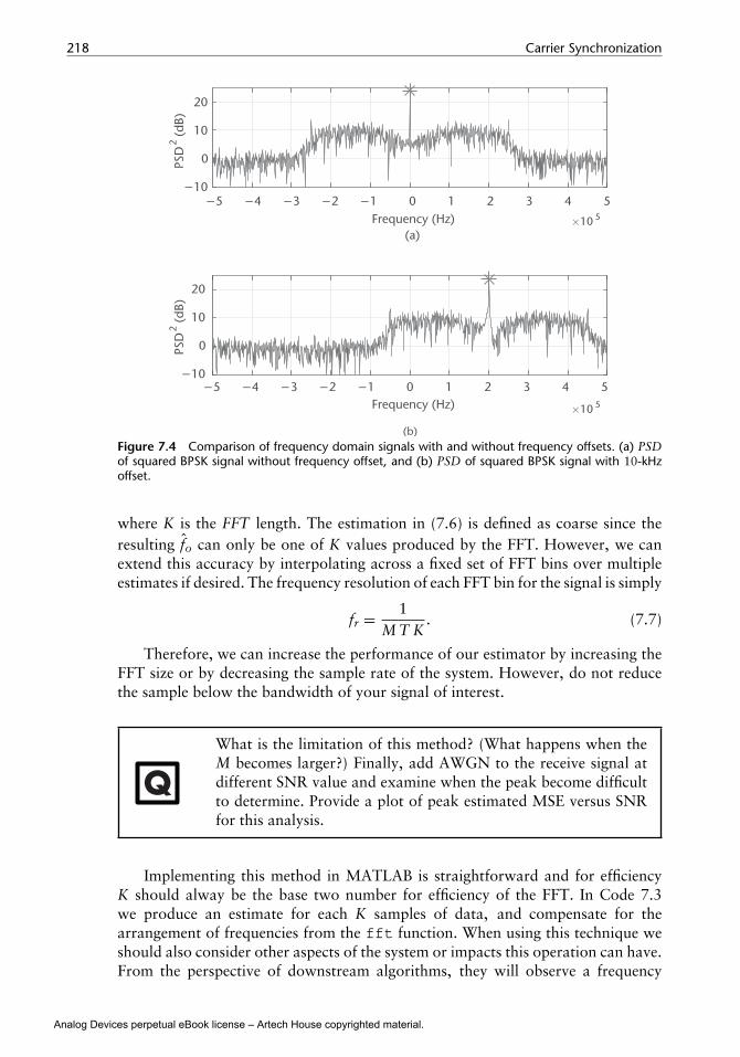
Alternatively, blind or nondata-aided (NDA) methods can operate over theentire duration of the signal. Therefore, it can be argued in a realistic system NDAcan outperform DA algorithms. These coarse techniques are typically implementedin an open-loop methodology, for ease of use. Here we will both outline andimplement a NDA FFT-based technique for coarse compensation. The conceptapplied here is straightforward, and based on our initial inspection provided inFigure 7.3, we can provide a rough estimate on the symbols offsets. However,directly taking the peak from the FFT will not be very accurate, especially if thesignal is not symmetrical in frequency. To compensate for this fact, we will removethe modulation components of the signal itself by raising the signal to its modulationorder M. From our model in (7.2), ignoring noise, we can observe the following:
rM(k) = sM(k)ej(2π fokT+θ)M. (7.5)
This will shift the offset to M times its original location and make s(t) purely realor purely complex. Therefore, the sM(t) term can be ignored and only the remainingexponential or tone will remain. To estimate the position of this tone we will takethe FFT of rM(t) and relate the bin with the most energy to the location of this tone.Figure 7.4 is an example frequency plot of rM(t) for a BPSK signal generated fromthe MATLAB Code 7.2 offset by 10 kHz. The peak is clearly visible at twice thisfrequency as expected. Formally this frequency estimation can be written in a singleequation as [4]
fo = 12 T K
arg∣∣K−1∑k=0
rM(k)e−j2πkT/K∣∣ (7.6)
Analog Devices perpetual eBook license – Artech House copyrighted material.
Wyglinski: “ch07_new” — 2018/3/26 — 11:43 — page 218 — #6
218 Carrier Synchronization
Figure 7.4 Comparison of frequency domain signals with and without frequency offsets. (a) PSDof squared BPSK signal without frequency offset, and (b) PSD of squared BPSK signal with 10-kHzoffset.
where K is the FFT length. The estimation in (7.6) is defined as coarse since theresulting fo can only be one of K values produced by the FFT. However, we canextend this accuracy by interpolating across a fixed set of FFT bins over multipleestimates if desired. The frequency resolution of each FFT bin for the signal is simply
fr = 1M T K
. (7.7)
Therefore, we can increase the performance of our estimator by increasing theFFT size or by decreasing the sample rate of the system. However, do not reducethe sample below the bandwidth of your signal of interest.
Q
What is the limitation of this method? (What happens when theM becomes larger?) Finally, add AWGN to the receive signal atdifferent SNR value and examine when the peak become difficultto determine. Provide a plot of peak estimated MSE versus SNRfor this analysis.
Implementing this method in MATLAB is straightforward and for efficiencyK should alway be the base two number for efficiency of the FFT. In Code 7.3we produce an estimate for each K samples of data, and compensate for thearrangement of frequencies from the fft function. When using this technique weshould also consider other aspects of the system or impacts this operation can have.From the perspective of downstream algorithms, they will observe a frequency
Analog Devices perpetual eBook license – Artech House copyrighted material.

Wyglinski: “ch07_new” — 2018/3/26 — 11:43 — page 219 — #7
7.2 Frequency Offset Compensation 219
Code 7.3 fftFreqEst.m
1 %% Estimation of error2 fftOrder = 2ˆ10; k = 1;3 frequencyRange = linspace(-sampleRateHz/2,sampleRateHz/2,fftOrder);4 % Precalculate constants5 offsetEstimates = zeros(floor(length(noisyData)/fftOrder),1);6 indexToHz = sampleRateHz/(modulationOrder*fftOrder);7 for est=1:length(offsetEstimates)8 % Increment indexes9 timeIndex = (k:k+fftOrder-1).’;
10 k = k + fftOrder;11 % Remove modulation effects12 sigNoMod = offsetData(timeIndex).ˆmodulationOrder;13 % Take FFT and ABS14 freqHist = abs(fft(sigNoMod));15 % Determine most likely offset16 [˜,maxInd] = max(freqHist);17 offsetInd = maxInd - 1;18 if maxInd>=fftOrder/2 % Compensate for spectrum shift19 offsetInd = offsetInd - fftOrder;20 end21 % Convert to Hz from normalized frequency index22 offsetEstimates(est) = offsetInd * indexToHz;23 end
correction every K samples. Ideally fo remains constant, but this is unlikely ifthe offset is close to an FFT bin boundary. Resulting is frequency jumps in thesignal ±fr from previous signals. Unfortunately these abrupt changes can disruptfeedback algorithm downstream, which are ill-equipped to deal to sudden shift infrequency or phase of the signal they are estimating/correcting. To combat this wehave two main strategies. First, the estimates can be averaged over time with a filter,smoothing out the changes over time. The second option would be to only applythis correction at the start of a frame. Since the offset should be relatively stationaryacross a reasonably sized frame, a single measurement should be accurate over thatduration of time. This correction is also considered coarse since it can only beaccurate to within fr, which only enforces this type of correction interval.
With that said a weakness of this FFT-based technique is that it requiresa significant amount of data for a reasonable estimate. This technique willalso produce unpure tones when oversampled at the transmitter with transmitfilters. However, other techniques such as from Luise [5] are designed for burst-type applications where less data relative to the FFT method above is required.Unfortunately, the Luise method is a biased estimator unlike the FFT method.
7.2.2 Fine Frequency CorrectionAfter coarse frequency correction (CFC) there will still be offset based on theconfigured resolution chosen fr. Fine frequency correction (FFC), also called carrierphase correction, should produce a stable constellation for eventual demodulation.Essentially this will drive the remaining frequency offset of the received signal tozero. We can describe this correction as producing a stable constellation due to howfine frequency offset effects are typically examined with a constellation diagram. If a
Analog Devices perpetual eBook license – Artech House copyrighted material.

Wyglinski: “ch07_new” — 2018/3/26 — 11:43 — page 220 — #8
220 Carrier Synchronization
Q
Using loopback with Pluto SDR and Code 7.3, measure thefrequency estimate’s mean squared error as a function of thedifference between the center frequencies (fo,max) of the transmitterand receiver. Use BSPK signal here and examine f� from 0 − 100kHz at 1-MHz baseband sampling rate.Repeat this, but fix the transmitter to a gain of −30 and takeestimates with the receiver in manual gain mode at 10, 30, and 50.
discrete digitally modulated signal exhibits frequency offset, this will cause rotationover time as examined in a constellation diagram. In Figure 7.5 we demonstratethis effect where each number relates a sample’s relative occurrence in time, whichprovides this perspective of rotation. The signal itself is BPSK, causing it to jumpacross the origin with different source symbols. If a positive frequency offset isapplied the rotation will be counterclockwise and clockwise with a negative offset.The rate of the rotation is equal to the frequency offset, which is where our notionof ω (angular frequency) comes from, as previously defined in (7.3).
This offset can also be observed with Pluto SDR in a similar way. In Figure 7.6we transmitted a BPSK signal in loopback with 1-kHz difference between transmitand receive LOs. We observe a similar rotation as in Figure 7.5 in Figure 7.6(b). Inorder to correctly visualize this effect we needed to perform timing correction, whichwas borrowed from Chapter 6. Without timing correction the signal is difficultto interpret from the constellation plot as observed in Figure 7.6(a). Since timingcorrection was performed in this case before the frequency was corrected, thisrequired use of the Gardner technique as detailed in Section 6.4.1. Unlike CFC,
Figure 7.5 Rotating constellation of BPSK source signal with frequency offset.
Analog Devices perpetual eBook license – Artech House copyrighted material.

Wyglinski: “ch07_new” — 2018/3/26 — 11:43 — page 221 — #9
7.2 Frequency Offset Compensation 221
Figure 7.6 BPSK signal transmit through Pluto SDR in loopback with 1-kHz offset at 1 MHz. (a)BPSK signal before timing correction, and (b) BPSK signal after timing correction.
which uses a feedforward technique, for FFC we will utilize a feedback or closed-loop method based PLL theory as examined in Chapter 4. The structure of thisalgorithm is provided in Figure 6.11 derived from [6, Chapter 7], which relatesback our original outline in Figure 6.11.
This all-digital PLL-based algorithm works by first measuring the phase offsetof a received sample in the phase error detector (PED), which we call the errorsignal e(n). The PED is designed based on the structure of the desired receiveconstellation/symbols. Next, the loop filter helps govern the dynamics of the overallPLL. The loop filter can determine operational frequency (sometimes called pull-in range), lock time, and responsiveness of the PLL, as well as smoothing out theerror signal. Finally, we have the direct digital synthesizer (DDS), whose name isa remnant of analog PLL designs with voltage-controlled oscillators (VCOs). TheDDS is responsible for generation of the correction signal for the input, whichagain will be fed back into the system. In the case of the FFC design, this PLLshould eventually produce an output signal with desired offset equal to zero.
Starting with the PED, the goal of this block is simply to measure the phase orradial offset of the input complex data from a desired reference constellation. Byreference and by extension e(n), we are actually referring to the distance from theconstellation bases. In the case of QAM, PSK, and PAM these will always be thereal and imaginary axes. However, you may need to extend this perspective withregard to FSK or other modulation schemes. The primary reasoning behind thisidea is that it will remove the scaling aspect in a specific dimension, and insteadconsider the ratio of energy or amplitude in a specific basis. To better understandthis concept let us consider QPSK, which has the following PED equation:
e(n) = sign(Re(y(n))) × Im(y(n)) − sign(Im(y(n))) × Re(y(n)). (7.8)
In (7.8) e(n) is essentially measuring the difference between the real andimaginary portions of y(n), and will only be zero when Re(y(n)) = Im(y(n)). Youwill notice that this will force the output constellation only to a specific orientation,
Analog Devices perpetual eBook license – Artech House copyrighted material.

Wyglinski: “ch07_new” — 2018/3/26 — 11:43 — page 222 — #10
222 Carrier Synchronization
but not a specific norm value. However, if y(n) requires a different orientation thiscan be accomplished after passing through the synchronizer with a simple multiplywith the desired phase shift of φPOST as
ySHIFT(n) = y(n)ej∗φPOST . (7.9)
Note that ySHIFT(n) should not be fed into the PED.In the case of other modulation schemes the PED error estimation will change
based on the desired signal arrangement. BPSK or PAM for example will have thefollowing error estimation:
e(n) = sign(Re(y(n))) × Im(y(n)). (7.10)
This PED error function again has the same goal of providing the error signalonly for the orientation of y(n). For (7.10) e(n) will only be zero when y(n) is purelyreal.
The reasoning behind (7.8) and (7.10) is straightforward. On the other hand,the loop filter in all PLL designs is the most challenging aspect, but it provides themost control over the adaptation of the system. Again here we will use a PI filteras our loop filter, which was detailed in Section 6.3.1. The last piece to this FFCsynchronizer is the DDS, which is just an integrator. Since the loop filter producesa control signal, which is equivalent to the frequency of the input signal, it becomesnecessary to extract the phase of this signal instead. The transfer functions used forthe integrator here are
D(s) = G31s
→ D(z) = G3z−1
1 − z−1 . (7.11)
Note that we have added an additional delay of a single sample in the discretedomain, and since we are producing a correction signal G3 = −1. Again thisintegrator can be implemented with a biquad filter.
In this arrangement of the PLL shown in Figure 7.7, the system should producean output y(n), which has minimal phase and frequency offsets. Going around theloop again in Figure 7.7, the PED will first produce an error equal to the phaseoffset associated with the observed corrected1 symbol y(n), then the loop filter willrelate this observed error and weight it against all previous errors. Finally, the DDSwill convert the weighted error/control signal f (n) to a phase φ(n), which we useto correct the next input sample x(n + 1). In the case of frequency offsets, φ willcontinuously change since is it a phase value, not a frequency value. However, ifthe input signal is too dynamic or the gains of the filters are not set appropriately,the PLL will not be able to keep up with the changing phase (frequency) of x.
For the calculation of the gain values (G1, G2) of the loop filter, utilize thefollowing equations based on a preferred damping factor ζ and loop bandwidthBLoop:
θ = BLoop
M(ζ + 0.25/ζ )� = 1 + 2ζθ + θ2 (7.12)
1. We define this as a corrected symbol since it has passed through the rotator and we will not apply additionalphase shifts to this sample. This is also the output of the PLL.
Analog Devices perpetual eBook license – Artech House copyrighted material.

Wyglinski: “ch07_new” — 2018/3/26 — 11:43 — page 223 — #11
7.2 Frequency Offset Compensation 223
Figure 7.7 FFC structure based on PLL design for feedback corrections.
G1 = 4ζθ/�
M KG2 = (4/M)θ2/�
M K(7.13)
where M is the number of sample per symbol and K is the detector gain. ForQPSK and rectangular QAM K = 2, but for PAM and PSK K = 1. Note thatBLoop is a normalized frequency. If you are interested in how these are derived,consult [6, Appendix C] for a full detailed analysis. For the selection of ζ refer backto Section 6.3.1, which has the same definition here. The selection of BLoop shouldbe related to the maximum estimated normalized frequency locking range �f ,lockrange desired:
�f ,pull ∼ 2π√
2ζBLoop. (7.14)
Note that this value is an estimate based off a linearized model of the PLL.Therefore inconsistencies may exist in the simulated versions. However, this PLLdesign should perform well even under strong noise conditions when configuredcorrectly. Unlike the CFC correction this FFC will generally not have the sameoperational range. In your designs, it may be useful to start with a damping factorof ζ = 1 and a loop bandwidth of BLoop = 0.01. From experience, using anoverdamped system here is preferable since it directly increases the pull-in range.However, it will take the loop longer to converge.
QStarting from Code 7.4 implement a carrier recovery algorithmfor BPSK. Tune this implementation for a normalized frequencyoffset of 0.001 and 0.004. Evaluate these implementations over arange of SNR for the MSE of their frequency estimates.
We now have all the necessary pieces to implement the FFC synchronizer,for which we provide a full reference implementation in Code 7.4. However, itis important to discuss some of the design considerations. First, we have statedthe output of the FFC synchronizer can have a target of a specific orientation ofthe output constellation, which is solely determined by the PED. However, thesynchronizer may not always be able to achieve this target constellation orientation,meaning the constellation may appear slightly rotated or appear at multiples ofthe expected position. This will result from signals with larger carrier offsetsthan the FFC was configured to handle or most notably when the system isconfigured in an underdamped way. Alternatively, if the received signal has poor
Analog Devices perpetual eBook license – Artech House copyrighted material.
Wyglinski: “ch07_new” — 2018/3/26 — 11:43 — page 224 — #12
224 Carrier Synchronization
SNR this will also degrade the effective pull-in-range of the synchronize of cause anondesirable lock position. This is illustrated in Code 7.4, where two different ζ
configurations are used. The system is also driven close to the estimated maximumoffset for the configuration. In general these estimates will be conservative andwill require empirical testing for a specific modulation scheme, SNR, and loopfilter configuration. However, in this case if we examine the converged signals inFigure 7.8 we notice an interesting set of outcomes. In Figure 7.8(b) the constellationactually converges to a false minimum. This is a result of the dynamics of the PLL,which is in an underdamped state. Forcing the system to be more rigid will providethe correct result as in Figure 7.8(a). However, if ζ is too large the synchronize willnot converge or can take a very long time to do so.
Q
Introduce timing offset into the model for Code 7.4. For therecovery process take your implementation from Chapter 4 fortiming recovery and place this into the system. Evaluate theseimplementations over a range of SNR for the MSE of theirfrequency estimates.
When implementing and testing your own system it can be useful to actuallymeasure the frequency estimation of the synchronizer itself. Since we know that theoutput of the DDS φ is the instantaneous phase correction needed for the nextsymbol, we can simply apply (7.3) with similar computations as in Code 7.1.From the angular frequency estimates we can translate this to a more tangiblefrequency estimate in hertz as in (7.3). From inspecting the derivative of Phase(φ) for Code 7.4 we can examine the convergence of the estimate for an offset of20 Hz with fs = 1000 Hz. In Figure 7.9 we plot fest where there is an obviousconvergence around the correct value. However, since the signal contains noise andthere is inherent noise to the PLL, the estimate will not be static. This is useful ina real system since the offsets between transmitter and receiver LOs will always bedynamic with respect to one another.
7.2.3 Performance AnalysisTo evaluate the synchronization performance a number of variables can beconsidered. These include but are not limited to lock time, effective pull-in range,and converged error vector magnitude (EVM). These metrics should be balancedin a way that meets the needs for a specific design since they will clash with oneanother. For example, it can be simple to design a system with a fast lock time,but it will probably have limited pull-in range. This is a direct relation to (7.14)and a secondary measurement from [6, Appendix C], which defines the normalizedfrequency lock delay:
t�,Max ∼ 32ζ 2
BLoop. (7.15)
We can demonstrate this trade-off between ζ and BLoop if we focus on the errorsignal directly from the PED. Modifying the code from 7.4 by fixing the normalizedcarrier offset to 0.01, ζ = 1.3, and selecting two different values for BLoop we
Analog Devices perpetual eBook license – Artech House copyrighted material.

Wyglinski: “ch07_new” — 2018/3/26 — 11:43 — page 225 — #13
7.2 Frequency Offset Compensation 225
Figure 7.8 Converged QPSK signals after carrier recovery with different damping factors, both(a) overdamped (ζ = 1.3), and (b) underdamped (ζ = 0.9).
Figure 7.9 Estimations over time and eventual convergence of implemented FFC for 20-Hz offset.
Q
Based off your existing simulation solutions that recover signalswith both timing and carrier offset, introduce Pluto SDRas the channel mechanism. It may be useful to start withCode 6.1 and 7.4. Evaluate your implementation in loopback withincreasing frequency difference between transmit and receive LOs.
can observe e(n) in Figure 7.10. In both configurations of BLoop the normalizedoffset is less than �f ,pull. In the case for BLoop = 0.24, the system converges to asolution within a few tens of samples, while the BLoop = 0.03 case is an order ofmagnitude slower. However, the variance of the converged error signal σ 2
e is threetimes smaller for the case when BLoop = 0.03. This error will appear as phase noiseon y(n), which will affect the demodulation correctness of the signal.
Analog Devices perpetual eBook license – Artech House copyrighted material.

Wyglinski: “ch07_new” — 2018/3/26 — 11:43 — page 226 — #14
226 Carrier Synchronization
Figure 7.10 Error signal from QPSK PED for different loop bandwidth for time. (a) BLoop = 0.24with σ 2
e = 0.0103 after convergence, and (b) BLoop = 0.03 with σ 2e = 0.0031 after convergence.
7.2.4 Error Vector Magnitude MeasurementsEvaluating the EVM for y(n) will provide a measure of this phase noise in therecovered signal. EVM is a very useful measurement to understand the algorithmicperformance in the system. EVM measures the residual error of the constellationwith respect to a reference position. To calculate EVM in percent RMS we can usethe following equation:
EVMRMS = 100 ×√√√√N−1∑
k=0
econst(k)
N−1∑k=0
(Re(y(k))2 + Im(y(k))2), (7.16)
where
econst(k) = (Re(y(k)) − Re(y(k)))2 + (Im(y(k)) − Im(y(k)))2 (7.17)
and y(k) is the reference symbol for y(k). EVM is a measure on the dispersivenessof the received signal. Therefore, the lower the EVM values the better. In somesituations it can be useful to calculate EVM in decibels, which can be converted
Analog Devices perpetual eBook license – Artech House copyrighted material.

Wyglinski: “ch07_new” — 2018/3/26 — 11:43 — page 227 — #15
7.2 Frequency Offset Compensation 227
Code 7.4 badlock.m
1 %% General system details
2 sampleRateHz = 1e6; samplesPerSymbol = 1; frameSize = 2ˆ10;
3 numFrames = 10; nSamples = numFrames*frameSize;
4 DampingFactors = [0.9,1.3]; NormalizedLoopBandwidth = 0.09;
5 %% Generate symbols
6 order = 4; data = pskmod(randi([0 order-1], nSamples, 1),order,0); % QPSK
7 %% Configure LF and PI
8 LoopFilter = dsp.IIRFilter(’Structure’, ’Direct form II transposed’, ...
9 ’Numerator’, [1 0], ’Denominator’, [1 -1]);
10 Integrator = dsp.IIRFilter(’Structure’, ’Direct form II transposed’, ...
11 ’Numerator’, [0 1], ’Denominator’, [1 -1]);
12 for DampingFactor = DampingFactors
13 %% Calculate range estimates
14 NormalizedPullInRange = min(1, 2*pi*sqrt(2)*DampingFactor*...
15 NormalizedLoopBandwidth);
16 MaxFrequencyLockDelay = (4*NormalizedPullInRangeˆ2)/...
17 (NormalizedLoopBandwidth)ˆ3;
18 MaxPhaseLockDelay = 1.3/(NormalizedLoopBandwidth);
19 %% Impairments
20 frequencyOffsetHz = sampleRateHz*(NormalizedPullInRange);
21 snr = 25; noisyData = awgn(data,snr);% Add noise
22 % Add frequency offset to baseband signal
23 freqShift=exp(1i.*2*pi*frequencyOffsetHz./sampleRateHz*(1:nSamples)).’;
24 offsetData = noisyData.*freqShift;
25 %% Calculate coefficients for FFC
26 PhaseRecoveryLoopBandwidth = NormalizedLoopBandwidth*samplesPerSymbol;
27 PhaseRecoveryGain = samplesPerSymbol;
28 PhaseErrorDetectorGain = log2(order); DigitalSynthesizerGain = -1;
29 theta = PhaseRecoveryLoopBandwidth/...
30 ((DampingFactor + 0.25/DampingFactor)*samplesPerSymbol);
31 delta = 1 + 2*DampingFactor*theta + theta*theta;
32 % G1
33 ProportionalGain = (4*DampingFactor*theta/delta)/...
34 (PhaseErrorDetectorGain*PhaseRecoveryGain);
35 % G3
36 IntegratorGain = (4/samplesPerSymbol*theta*theta/delta)/...
37 (PhaseErrorDetectorGain*PhaseRecoveryGain);
38 %% Correct carrier offset
39 output = zeros(size(offsetData));
40 Phase = 0; previousSample = complex(0);
41 LoopFilter.release();Integrator.release();
42 for k = 1:length(offsetData)-1
43 % Complex phase shift
44 output(k) = offsetData(k+1)*exp(1i*Phase);
45 % PED
46 phErr = sign(real(previousSample)).*imag(previousSample)...
47 - sign(imag(previousSample)).*real(previousSample);
48 % Loop Filter
49 loopFiltOut = step(LoopFilter,phErr*IntegratorGain);
50 % Direct Digital Synthesizer
51 DDSOut = step(Integrator,phErr*ProportionalGain + loopFiltOut);
52 Phase = DigitalSynthesizerGain * DDSOut;
53 previousSample = output(k);
54 end
55 scatterplot(output(end-1024:end-10));title(’’);
56 end
Analog Devices perpetual eBook license – Artech House copyrighted material.

Wyglinski: “ch07_new” — 2018/3/26 — 11:43 — page 228 — #16
228 Carrier Synchronization
from (7.16) as
EVMdB = 20 log10
(EVMRMS
100
). (7.18)
Calculating EVM in decibels is very common in OFDM standards due to high-orderconstellations that can be transmitting, which require a significant EVM marginto recover. For convience, the Communications System Toolbox include a systemobject called comm.EVM to provide these calculations for us.
QStarting with Code 7.4, evaluate the EVM of converged signalswith regard to ζ and BLoop. Select values of ζ in underdamped,overdamped, and critically damped configurations.
7.3 Phase Ambiguity
The last topic to consider for carrier synchronization is phase ambiguity. Phaseambiguity arises from the fact that the FFC synchronizer outlined here is blind tothe true orientation of the transmitted signal. For a given symmetrical modulationscheme there can be a number of convergent orientations, which can be relatedto the modulation order. For example, PAM will have two possible orientations,QPSK and rectangular QAM will have four, while MPSK with have M possibleorientations. However, there are a number of solutions to compensate for thisproblem, which includes code words, use of an equalizer with training data, anddifferential encoding. There are different use cases for each implementation.
7.3.1 Code WordsThe use of code words is a common practice for resolution of phase ambiguity,which relies on a known sequence in the received data. This is typically just thepreamble itself, which will exist in each frame and is known at the receiver. Thisstrategy can be used before or after demodulation if desired. If performed postdemodulation, the output bits must be remapped onto their true positions. Thisprocess is best explained through an example. Consider the source words w andassociated QPSK symbols s:
w = [1, 0, 3] s = [(−1, 1i) (1, 1i) (−1, −1i)]. (7.19)
The possible received symbols would be
s1 = [(−1, 1i) (1, 1i) (−1, −1i)]s2 = [(−1, −1i) (−1, 1i) (1, −1i)]s3 = [(1, −1i) (−1, −1i) (1, 1i)]s4 = [(1, 1i) (1, −1i) (−1, 1i)].
(7.20)
Demodulating each code word symbol and comparing with the expected resultwould provide the necessary mapping to correctly demodulate the remaining datasymbols. For an implementation it would be useful to demodulate all the preamble
Analog Devices perpetual eBook license – Artech House copyrighted material.

Wyglinski: “ch07_new” — 2018/3/26 — 11:43 — page 229 — #17
7.4 Chapter Summary 229
symbols and take the most common orientation mapping, since relying on a singlesymbol can be error-prone.
Alternatively, the phase offset θp from the correct orientation can be measureddirectly where p is the received preamble symbols, pr is the reference or truepreamble symbols, and the correction required is simply
θp = tan−1(∑
n
Im(p(n)∗ × pr(n))
Re(p(n)∗ × pr(n))
), (7.21)
assuming p(n) has a desirable orientation. Then the remaining signal y would becorrected as
yc = y e−jθp . (7.22)
7.3.2 Differential EncodingThe second option to deal with phase ambiquity is to differentially encode the sourcebits themselves. The goal here is to make the true data dependent on the differencebetween successive bits, not on the received bits themselves. To encode the sourcedata we apply the following at the transmitter:
bt(n) = bt(n − 1) ⊕ b(n), (7.23)
where bt are the transmitted encoded bits, b are the uncoded bits, and ⊕ is a modulotwo addition. To decode the signal we basically perform (7.23) in reverse as
b(n) = bt(n) ⊕ bt(n − 1). (7.24)
Usually in this scheme the first bit is ignored since it is only based on itself, notthe difference between two consecutive bits. Engineers may point to this as wasteful,but this reduces any complex mathematics associated with measuring offsets withsymbols and only requires bit-level operations. This can also reduces the bit errorrate of a received signal due to propagation of bit errors.
7.3.3 EqualizersThe third popular option is to rely on an equalizer to correct this ambiguity for thesystem. Using training data the equalizer can learn and correct for this phase shift,which in essence is just a complex multiplication. Equalizers will be discussed indetail in Chapter 9. However, this is a small task for an equalizer implementationif channel correct or synchronization are not performed by the equalizer as well.
7.4 Chapter Summary
In this chapter we have discussed and provided a model of carrier offset and howit relates to receiver operations. From this model we have provided two schemesfor compensating for carrier offset including coarse and fine recovery algorithms.However, other implementations do exist that can jointly perform timing and carrierrecovery [6] if desired. We have examined how these algorithms can be used at thesystem level, as well as how individual performance can be evaluated. These includecharacterization of their parameterization as well as metric on the recovered data.
Analog Devices perpetual eBook license – Artech House copyrighted material.

Wyglinski: “ch07_new” — 2018/3/26 — 11:43 — page 230 — #18
230 Carrier Synchronization
In summary, carrier offset compensation is a necessary synchronization techniquewhen transmitting data between two disjoint nodes with independent LOs.
References
[1] Analog Devices, Inc., ADALM-PLUTO SDR Active Learning Module,http://www.analog.com/media/en/news-marketing-collateral/product-highlight/ADALM-PLUTO-Product-Highlight.pdf.
[2] Oppenheim, A.V., and R.W. Schafer, Discrete-Time Signal Processing, Prentice Hall, 1989.[3] Morelli, M., and U. Mengali, “Feedforward Frequency Estimation for PSK: A Tutorial
Review,” European Transactions on Telecommunications, Vol. 9, No. 2, 1998,pp. 103–116.
[4] Wang, Y., K. Shi, and E. Serpedin,“Non-Data-Aided Feedforward Carrier FrequencyOffset Estimators for QAM Constellations: A Nonlinear Least-Squares Approach,”EURASIP Journal on Advances in Signal Processing, (2004) 2004: 856139,https://doi.org/10.1155/S1110865704403175.
[5] Luise, M. and R. Reggiannini, “Carrier Frequency Recovery in All-Digital Modems forBurst-Mode Transmissions,” IEEE Transactions on Communications, Vol. 43, No. 2,1995, pp. 1169–1178.
[6] Rice, M., Digital Communications: A Discrete-Time Approach, Third Edition,Pearson/Prentice Hall, 2009.
Analog Devices perpetual eBook license – Artech House copyrighted material.