
Soft-Switching Techniques
9
© 2012 IEEE Proceedings of the 38th Annual Conference of the IEEE Industrial Electronics Society (IECON 2012), Montreal, Canada, October 25-28, 2012. Soft-Switching Techniques for Medium-Voltage Isolated Bidirectional DC/DC Converters in Solid State Transformers G. Ortiz D. Bortis J. W. Kolar O. Apeldoorn This material is posted here with permission of the IEEE. Such permission of the IEEE does not in any way imply IEEE endorsement of any of ETH Zurich‘s products or services. Internal or personal use of this material is permitted. However, permission to reprint/republish this material for advertising or promotional purposes or for creating new collective works for resale or redistribution must be obtained from the IEEE by writing to [email protected]. By choosing to view this document, you agree to all provisions of the copyright laws protecting it.
-
Upload
shoaib-mughal -
Category
Documents
-
view
44 -
download
1
description
different techniques for soft switching are discussed.
Transcript of Soft-Switching Techniques

© 2012 IEEE
Proceedings of the 38th Annual Conference of the IEEE Industrial Electronics Society (IECON 2012), Montreal, Canada, October 25-28, 2012.
Soft-Switching Techniques for Medium-Voltage Isolated Bidirectional DC/DC Converters in Solid State Transformers
G. OrtizD. BortisJ. W. KolarO. Apeldoorn
This material is posted here with permission of the IEEE. Such permission of the IEEE does not in any way imply IEEE endorsement of any of ETH Zurich‘s products or services. Internal or personal use of this material is permitted. However, permission to reprint/republish this material for advertising or promotional purposes or for creating new collective works for resale or redistribution must be obtained from the IEEE by writing to [email protected]. By choosing to view this document, you agree to all provisions of the copyright laws protecting it.

Soft-Switching Techniques for Medium-Voltage Isolated BidirectionalDC/DC Converters in Solid State Transformers
G. Ortiz*, D. Bortis*, J. W. Kolar*, O. Apeldoorn***Power Electronic Systems Laboratory, ETH Zurich
**Power Electronics and Medium Voltage Drives, ABB Switzerland AGEmail: [email protected]
Abstract—Soft switching techniques are very attractive and oftenmandatory requirements in medium-voltage and medium-frequencyapplications such as solid state transformers. The effectiveness of thesesoft switching techniques is tightly related to the dynamic behavior ofthe internal stored charge in the utilized semiconductor devices. For thisreason, this paper analyzes the behavior of the internal charge dynamicsin high-voltage semiconductors, giving a clear base to understandthe previously proposed zero-current-switching techniques for IGBT-based resonant dual-active-bridges. From these previous approaches,the two main concepts that allow switching loss reduction in high-voltage semiconductors are identified: 1) shaping of the conductedcurrent in order to achieve a high recombination time in the previouslyconducting semiconductors and 2) achieving ZVS in the turning-ondevice. The means to implement these techniques in a triangular currentmode dual-active-bridge converter together with the benefits of theproposed approaches are analyzed and experimentally verified witha 1.7 kV IGBT-based NPC bridge. Additionally, the impact of themodified currents in the converter’s performance are quantified inorder to determine the benefits of the introduced concepts in the overallconverter.
I. INTRODUCTION
Transformers operating in line frequency (50/60Hz) are keycomponents within today’s electric power systems as they providethe link between grids with different voltage levels, namely high-voltage, medium voltage (MV) and low voltage (LV) grids. Thesetransformers however, are characterized by several limitations suchas large size/weight, ideally equal input and output active andreactive power, equal input and output operating frequency andtightly linked input and output voltages.
These limitations can be overcome by building a transformerbased on power electronic devices, i.e. a Solid State Transformer(SST). An example of a single-phase SST is shown in Fig. 1-a). Here, the medium-voltage side AC/AC converter is used toactively shape the input current iMV, for example, to reach a unitypower factor or in other cases, if a capacitive buffer is providedinside the AC/AC converter, to act as an active filter and/or astatic Var compensator. The link between the MV and the LVAC/AC converters is done through a transformer whose operatingfrequency fMF lies in the Medium Frequency (MF) range, thusachieving a small size/weight and a faster dynamic response. Onthe LV side, the characteristics of the output AC voltage, namelyamplitude uLV and frequency fLV, can be actively controlled withlittle dependency on the medium voltage side voltage uMV andfrequency fMV. These additional functionalities are envisioned asthe key enabling features for future compact traction solutions [1,2], grid integration of renewable energy generation [3–5] and smartgrid implementation [6, 7], among others.
One possible structure for the SST is a three-stage concept[6] presented in Fig. 1-b). In this concept, AC/DC MV and LVconverters are connected to the MV and LV AC grids respectively.The DC-links of these AC/DC converters are linked through ahigh power DC/DC converter, where the isolation and voltage
fMF >> f fMV LV,
AC
AC
AC
AC
uLV = uLV*
fLV = fLV*
Control
ComunicationiMV*
iLV
uLV*, fLV*
uMV
fMV
a)
ACDC DC
DC DCAC AC
ACuMV
fMV
uLV
b)
fLV
iMV
UMV,DC ULV,DC
DC DC/
MV side LV side
Figure 1: Solid state transformer: a) Single phase structure; b)Three-stage concept comprising high-power DC/DC converter.
step-down is provided through a MF AC-link. In the DC/DCconverter, the semiconductors in the MV side bridge are requiredto block voltages in the kilovolt range, therefore IGBTs are a veryattractive choice. These semiconductors however, are characterizedby a bipolar power stage which, in order to block these highvoltages, comprises a considerably large n− drift region whichstores a large amount of charge during the conduction phase of the
N1 N2
LrCr
UMV,DC ULV,DC
uLV,AC
is
uMV,AC
TST
S/2
t
UMV,DC
ULV,DC´
uLV,AC
is
uMV,AC
-UMV,DC
-ULV,DC´
a)
b)
´
Figure 2: Series resonant DAB: a) Power circuit linking MV to LVDC buses; b) Voltage and current in the AC link.

N1 N2
LsUMV,DC ULV,DC
isuMV,AC uLV,AC
TS
TS/2 t
UMV,DC
ULV,DC´
-UMV,DC
-ULV,DC´
a)
b)
uMV,AC
uLV,AC
is
´
Figure 3: Triangular current DAB: a) Power circuit linking MV toLV DC buses; b) Voltage and current in the AC link.
semiconductor. When the switch is turned-off, this stored chargeis evacuated from the semiconductor, causing tail currents whichoverlap with the blocking voltage, hence generating high switchinglosses. If operated in the MF range, these switching losses wouldbe unbearable, unless the current through the semiconductors isconveniently shaped during its conduction phase in order to achieveZero-Current-Switching (ZCS).
A widespread topology that can allow bidirectional power flowand ZCS operation, investigated mainly in traction applications,is the series resonant Dual Active Bridge (DAB) converter [1,8–12] (cf. Fig. 2). This topology consists of two active bridgeslinked through a MF transformer in series with a resonant tank.When operated below resonant frequency, this converter allowsthe MV and LV side switches to operate in ZCS, thus reducingtheir switching losses. Nevertheless, these switching losses arenot negligible in spite ZCS operation. For this reason, severalenhancements to the ZCS modulation scheme that allow a furtherreduction in the switching losses have been previously reported,whereby the main approaches are revised in this paper.
The main disadvantage of the series resonant DAB, besides itslower power density and high current requirement of the seriesresonant capacitor Cr, is its incapability to control the transferredpower while still achieving ZCS. In case power transfer controlis required, the Triangular Current Mode (TCM) DAB presents anattractive solution [13] (cf. Fig. 3). In this converter, the resonanttank is replaced by a series inductor Ls. By properly selecting thetransformer turns ratio, the MV side switches can be operated inZCS mode in both power directions while actively controlling thetransferred power by adjusting the LV side duty cycle [14, 15]. Inthis case however, ZCS on the LV side is not possible.
In this paper, an initial analysis on the stored charge dynamicsin high-voltage semiconductor devices is performed in Section II,which gives the base to study in Section III the previously proposedZCS methods in series resonant DABs. With this revision, novelconcepts for switching-loss reduction in the TCM DAB converter bymeans of soft switching techniques are proposed and experimentallyvalidated in Section IV. The reduction in switching losses in theMV side of the TCM DAB results in modified current shapes in theconverter, therefore the impact of these new current shapes in theoverall converter performance is quantitatively studied at the endof Section IV.
150
100
50
150
0
0
75
50
25
75
0
0C
urr
ent
[A]
Curr
ent
[A]
Char
ge
[C
]μ
Char
ge
[C
]μ
0 20 2510 155
Δ μT [ s]
100
50
50
25
b)a)
is
is
QE
Q
QE
Q
iS1
UMV,DC
S1
DUT
is
S1
iS1
toff TS/2
c)
d)
0
is
ΔT
Figure 4: In order to measure the semiconductor’s stored charge, thecircuit in a) was used. The triangular current shape shown in b) isgenerated by the current source is in a) and is used to measured
stored charge in 1.7 kV IGBTs for c) 25 ◦C and d) 120 ◦C junctiontemperature.
II. SEMICONDUCTOR STORED CHARGE DYNAMICS
High voltage bipolar semiconductor devices, as previously men-tioned, store large amounts of charge during their conductionphases. This charge, if not allowed to recombine internally, istranslated into switching losses when the device is taken back tothe blocking state. Since this stored charge is directly related tothe dissipated energy during the switching process, it is useful toanalyze the behavior of the charge Q stored in the switch duringits conduction phase.
Consider the circuit depicted in Fig. 4-a) where an IGBT-based bridge leg is presented. Here, a current source generates thetriangular current is shown in Fig. 3-b) whereby switch S1 is turnedon at t = 0, the beginning of the switching period, and turned-offat t = ∆T . By increasing stepwise the value of ∆T from ∆T = 0to ∆T = toff, the current turned-off by device S1 is modified,as shown in Fig. 4-b). Measuring the current iS1 through S1 andintegrating it during the switching process for each value of ∆T ,the charge stored in the device during the conduction phase can beconstructed.
This experiment was performed on a bridge leg based on 1.7 kVPT IGBTs (FF150R17KE4) operating at 20 kHz with a DC-linkvoltage of UMV,DC = 1kV and reaching a peak current of 140A.The results for the behavior of the charge Q for junction tem-peratures of 25 ◦C and 120 ◦C are presented in Figs. 4-c) and d)respectively.
From Fig. 4-c) it can be seen that the stored charge Q is notproportional to the conducted current, therefore it can be alreadyconcluded that switching losses under these conditions do notdepend on the instantaneous value of the switched current. This
iS1
UMV,DC
iS2
uS1
uS2
t tt
S1
S2S1 S1S1
S2 S2S2
uS1 uS1uS1
iS1iS1
iS1
uS2uS2uS2iS2 iS2
iS2
a) b) c) d)t1 t2 t3 t4 t2 t3 t4 t1 t2 t3 t4
is
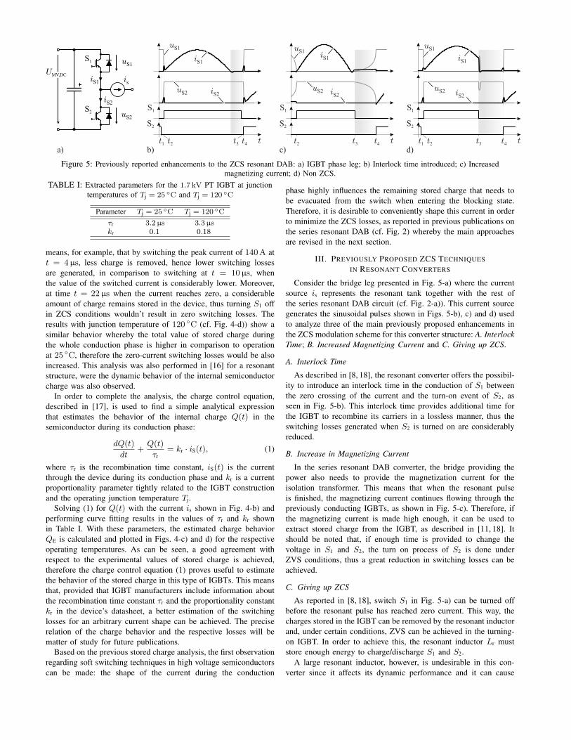
Figure 5: Previously reported enhancements to the ZCS resonant DAB: a) IGBT phase leg; b) Interlock time introduced; c) Increasedmagnetizing current; d) Non ZCS.
TABLE I: Extracted parameters for the 1.7 kV PT IGBT at junctiontemperatures of Tj = 25 ◦C and Tj = 120 ◦C
Parameter Tj = 25 ◦C Tj = 120 ◦C
τr 3.2µs 3.3µskr 0.1 0.18
means, for example, that by switching the peak current of 140A att = 4µs, less charge is removed, hence lower switching lossesare generated, in comparison to switching at t = 10µs, whenthe value of the switched current is considerably lower. Moreover,at time t = 22µs when the current reaches zero, a considerableamount of charge remains stored in the device, thus turning S1 offin ZCS conditions wouldn’t result in zero switching losses. Theresults with junction temperature of 120 ◦C (cf. Fig. 4-d)) show asimilar behavior whereby the total value of stored charge duringthe whole conduction phase is higher in comparison to operationat 25 ◦C, therefore the zero-current switching losses would be alsoincreased. This analysis was also performed in [16] for a resonantstructure, were the dynamic behavior of the internal semiconductorcharge was also observed.
In order to complete the analysis, the charge control equation,described in [17], is used to find a simple analytical expressionthat estimates the behavior of the internal charge Q(t) in thesemiconductor during its conduction phase:
dQ(t)
dt+
Q(t)
τr= kr · iS(t), (1)
where τr is the recombination time constant, iS(t) is the currentthrough the device during its conduction phase and kr is a currentproportionality parameter tightly related to the IGBT constructionand the operating junction temperature Tj.
Solving (1) for Q(t) with the current is shown in Fig. 4-b) andperforming curve fitting results in the values of τr and kr shownin Table I. With these parameters, the estimated charge behaviorQE is calculated and plotted in Figs. 4-c) and d) for the respectiveoperating temperatures. As can be seen, a good agreement withrespect to the experimental values of stored charge is achieved,therefore the charge control equation (1) proves useful to estimatethe behavior of the stored charge in this type of IGBTs. This meansthat, provided that IGBT manufacturers include information aboutthe recombination time constant τr and the proportionality constantkr in the device’s datasheet, a better estimation of the switchinglosses for an arbitrary current shape can be achieved. The preciserelation of the charge behavior and the respective losses will bematter of study for future publications.
Based on the previous stored charge analysis, the first observationregarding soft switching techniques in high voltage semiconductorscan be made: the shape of the current during the conduction
phase highly influences the remaining stored charge that needs tobe evacuated from the switch when entering the blocking state.Therefore, it is desirable to conveniently shape this current in orderto minimize the ZCS losses, as reported in previous publications onthe series resonant DAB (cf. Fig. 2) whereby the main approachesare revised in the next section.
III. PREVIOUSLY PROPOSED ZCS TECHNIQUES
IN RESONANT CONVERTERS
Consider the bridge leg presented in Fig. 5-a) where the currentsource is represents the resonant tank together with the rest ofthe series resonant DAB circuit (cf. Fig. 2-a)). This current sourcegenerates the sinusoidal pulses shown in Figs. 5-b), c) and d) usedto analyze three of the main previously proposed enhancements inthe ZCS modulation scheme for this converter structure: A. InterlockTime; B. Increased Magnetizing Current and C. Giving up ZCS.
A. Interlock Time
As described in [8, 18], the resonant converter offers the possibil-ity to introduce an interlock time in the conduction of S1 betweenthe zero crossing of the current and the turn-on event of S2, asseen in Fig. 5-b). This interlock time provides additional time forthe IGBT to recombine its carriers in a lossless manner, thus theswitching losses generated when S2 is turned on are considerablyreduced.
B. Increase in Magnetizing Current
In the series resonant DAB converter, the bridge providing thepower also needs to provide the magnetization current for theisolation transformer. This means that when the resonant pulseis finished, the magnetizing current continues flowing through thepreviously conducting IGBTs, as shown in Fig. 5-c). Therefore, ifthe magnetizing current is made high enough, it can be used toextract stored charge from the IGBT, as described in [11, 18]. Itshould be noted that, if enough time is provided to change thevoltage in S1 and S2, the turn on process of S2 is done underZVS conditions, thus a great reduction in switching losses can beachieved.
C. Giving up ZCS
As reported in [8, 18], switch S1 in Fig. 5-a) can be turned offbefore the resonant pulse has reached zero current. This way, thecharges stored in the IGBT can be removed by the resonant inductorand, under certain conditions, ZVS can be achieved in the turning-on IGBT. In order to achieve this, the resonant inductor Lr muststore enough energy to charge/discharge S1 and S2.
A large resonant inductor, however, is undesirable in this con-verter since it affects its dynamic performance and it can cause

problems related to the reverse recovery of the rectifying diodes.For this reason, turning-off S1, as shown in Fig. 5-d), does notresult in a traditional inductive switching. Nevertheless, this typeof switching strategy has reported reduction in switching losses inprevious implementations [8, 18] due to the additional time that canbe provided for carrier recombination (shaded area in Fig. 5-d)).
D. Applications to the TCM DAB converter
The aforementioned enhancements to the ZCS modulation inthe series resonant DAB suggest the use of similar techniquesin the TCM DAB. In case of the additional interlock time, itsimplementation in the TCM DAB is not straightforward. This isdue to the reverse recovery of the rectifying diodes in the LV side.In the resonant converter, the series inductor Lr is typically kept aslow as possible to improve the converter dynamic response. Thisresults in a large resonant capacitor Cr value, thus the peak voltagein this component is low in comparison to the DC-link voltages.The peak resonant capacitor voltage must be blocked by the diodesin the rectifying bridge after their respective conduction phases,therefore, since this voltage step is considerably low, the reverserecovery effects are negligible, as reported in [8, 11, 18].
On the other hand, in the TCM DAB, this voltage step isconsiderably larger as it corresponds to the MV side applied voltagetimes the turns ratio of the transformer, resulting in large oscillationsin the AC link voltages due to the reverse recovery of the rectifyingdiodes. Therefore, other strategies to provide longer recombinationtime need to be implemented in the case of the TCM DAB.
Since the value of the series inductor Ls in case of the TCMDAB is considerably higher than its resonant counterpart Lr, thestored energy in this component is considerably higher. This meansthat, by properly adjusting the control signals in the TCM DAB,the switches can perform switching of current, thus giving up ZCS,with high enough value to completely remove the stored charge inthe devices while achieving ZVS in the complementary switch. Thiscan be achieved without reducing the magnetizing inductance value,as in the series resonant DAB, and therefore without increasing thereactive power in the circuit. The modification to the modulationscheme that allows this behavior is introduced and experimentallyverified in the next section.
IV. PROPOSED ENHANCEMENTS TO THE TCM DAB
As discussed in the previous sections, there are two main strate-gies that can help to reduce switching losses in HV semiconductors.The first one is related to the time provided for the recombinationof the charge that the device stores during its conduction phaseby introducing a time interval before the semiconductor blockswhen the current is considerably lower than the peak current. Thesecond one is the reduction or total elimination of turn-on lossesby achieving ZVS in the turning-on device. This can be achievedby turning off a current (giving-up ZCS) through a modification inthe modulation scheme in the TCM DAB. The means to implementthese strategies will be discussed in this section together with theirexperimental verification.
A. Standard ZCS Modulation
In order to benchmark the proposed modulation strategies forthe TCM DAB, first the switching losses in the standard ZCSmodulation scheme studied in [13–15] were measured. Thesemeasurements were performed with 1.7 kV IGBTs (FF150R17KE4)which are based on field-stop technology. Because of its similarityto a punch-through IGBT, this technology is well suited for ZCSapplications due to its short recombination time [16, 17]. These
LsatLs
N1 N2UM
V,D
C=
2kV
S1
S2
S3
S4
UL
V,D
C=
400V
is
iS3
iS1
uS1
uS3
uMV,AC uLV,AC´
a)
b)
IGBT modules
Gate driverboard
Measurementboard
Figure 6: DAB converter used to test the 1.7 kV PT IGBTs: a)NPC-based bridge linked to the LV full-bridge through a
N1/N2 = 3/1 transformer; b) Hardware realization of the MV sideNPC 2 kV bridge.
1.7 kV IGBTs build a 2 kV NPC-based bridge as shown in Fig. 6-a) designed for nominal power of 166 kW and 20 kHz of switchingfrequency. The hardware realization of this bridge is shown inFig. 6-b). The non-linear inductor Lsat shown in Fig. 6-a) willbe used in the third part of this section to shape the current inorder to reduce the switching losses in the MV side switches. Thetransformer turns ratio is N1/N2 = 3/1 and the LV side bridge is a400V full-bridge structure utilized to generate the desired currentwaveforms. Planar current transformers and passive voltage probeswhere used to measure the currents and voltages respectively inswitches S1, S2, S3 and S4 (cf. Fig. 6-a)).
The operation of the bridge shown in Fig. 6 (without the saturableinductor Lsat) under ZCS was performed, as shown in Figs. 7 and 8.In Fig. 7-a) the operation during the positive semi cycle for powertransfer from MV to LV is shown. The cycle starts with zero currentthrough inductor Ls and the MV bridge applying positive voltageon its output while the LV side stays in freewheeling mode, thushalf of the MV side DC voltage is applied to inductor Ls causinga linearly increasing current. When the peak current is reachedaround t = 5µs, the LV side is switched and applies the LV DCvoltage on its output, thus the difference between the MV side DCvoltage and the reflected LV side DC voltage is applied to the seriesinductor Ls. Due to the transformer’s turns ratio N1/N2 = 3/1,this causes a voltage of −200V applied to the inductor Ls, hencethe current decreases linearly. As soon as the current reaches zero,

800 400
400 200
0 0
-400 -200
1200 600
1600 800V
olt
age
[V]
0 20 2510 155
Time [ s]μ
Curr
ent
[A]
uMV,ACuLV,AC´
a)
-200 -20
400 40
200 20
0 0
600 60
800 80
1200 120
1400 140
1000 100
Volt
age
[V]
0 21 3
Curr
ent
[A]
Time [ s]μ Time [ s]μb) c)
0 21 3
is
uS3
iS1
uS1 iS3
S turn-off /1 S turn-on3
Figure 7: Main waveforms in standard ZCS with TCM DAB andpower from MV side to LV side: a) AC-link waveforms for half
switching period; b) Voltage and current in S1 during the time instanthighlighted in a); c) Voltage and current in S3 during the time instant
highlighted in a).
both the MV and LV side bridges are switched to freewheeling, thusapplying zero voltage on their outputs while achieving ZCS. Theturn-off and turn-on process of complementary switches S1 and S3
respectively are used herein in order to exemplify the ZCS processand the further enhancements. It should be noted however that fora comprehensive switching loss analysis, all switching events weremeasured and used to calculate the total losses in the NPC bridge.
The switching process of devices S1 and S3 during the high-lighted time interval in Fig. 7-a) is shown in Figs. 7-b) and c)respectively. Here it can be seen that, since S1 was conducting thecurrent during the positive semi cycle, it contains a considerableamount of stored charge, which is removed when S3 is turned oncausing turn-off losses in S1 as well as considerable turn-on lossesin S3.
The current and voltage waveforms in the transformer for powerflowing from LV to MV are shown in Fig. 8-a), where the phaseshift and duty cycles of the LV and MV side bridges have beenadjusted to achieve the power flow in the reverse direction whilestill achieving ZCS in the MV side. The switching behavior ofswitches S1 and S3 is shown in Figs. 8-b) and c) respectivelywhere it should be noted that for this power direction the respectiveantiparallel diodes of each switch conduct the triangular current andare therefore responsible for the generated switching losses. As canbe seen, the turn-on process of S3 generates losses in the antiparalleldiode of S1, as this last device was previously conducting the fullcurrent thus it contains considerable amount of stored charge. Thecurrent peak in Figs. 8-b) and c) representing the evacuation ofcharge stored in the antiparallel diode of S1 flows through S3 duringits turn-on process, thus causing turn-on losses also in this lastdevice (cf. Fig. 8-c)).
The waveforms shown in Figs. 7 and 8 suggest the use of amodified modulation scheme where a certain amount of current isswitched-off by S1. This way, the stored charge accumulated duringits conduction phase is evacuated through the load, thus decreasingthe voltage of S3 before its gate signal is applied, thus achievingZVS in this last device and ideally a lossless commutation.
-200 -20
400 40
200 20
0 0
600 60
800 80
1200 120
1400 140
1000 100
Volt
age
[V]
0 1 2
Curr
ent
[A]
0 1 2
Time [ s]μ Time [ s]μb) c)
800 400
400 200
0 0
-400 -200
1200 600
1600 800
Volt
age
[V]
0 20 2510 155
Time [ s]μ
Curr
ent
[A]
a)
uMV,AC
-is
uLV,AC´
uS1
iS1
uS3
iS3
S turn-off /1 S turn-on3
Figure 8: Main waveforms in standard ZCS with TCM DAB andpower from LV side to MV side: a) AC-link waveforms for halfswitching period; b) Voltage and currents in S1 during the time
instant highlighted in a); c) Voltage and current in S3 during the timeinstant highlighted in a).
B. Modified ZVS Modulation
The operation under ZVS was studied for the converter displayedin Fig. 6 (without the saturable inductor Lsat). The waveforms forpower from MV to LV are shown in Fig. 9-a), where the duty cyclesand phase shift are adjusted in order to achieve ZVS in the MVside bridge. In this case, S1 is turned-off before the current reacheszero, thus loosing ZCS, as shown in Fig. 9-b). Since the current isnot zero when S1 is turned off, its voltage increases before the gatesignal is applied to its complementary switch S3. This means thatS3 is turned on with ZVS and no current peak must be conductedduring its turn-on process (cf. Fig. 9-c)), in contrast to the switchingprocess shown in Fig. 7-c), thus reducing the turn-on losses in S3
800 400
400 200
0 0
-400 -200
1200 600
1600 800
Volt
age
[V]
0 20 2510 155
Time [ s]μ
Curr
ent
[A]
a)
-200 -20
400 40
200 20
0 0
600 60
800 80
1200 120
1400 140
1000 100
Volt
age
[V]
0 21 3
Curr
ent
[A]
Time [ s]μ Time [ s]μb) c)
0 21 3
uS3uS1
uMV,AC´
is
uLV,AC
iS1 iS3
S turn-off /1 S turn-on3
Figure 9: Main waveforms in ZVS with TCM DAB and power fromMV side to LV side: a) AC-link waveforms for half switching period;b) Voltage and current in S1 during the time instant highlighted in a);c) Voltage and current in S3 during the time instant highlighted in a).

-200 -20
400 40
200 20
0 0
600 60
800 80
1200 120
1400 140
1000 100
Volt
age
[V]
0 1 2
Curr
ent
[A]
0 1 2
Time [ s]μ Time [ s]μb) c)
800 400
400 200
0 0
-400 -200
1200 600
1600 800V
olt
age
[V]
0 20 2510 155
Time [ s]μ
Curr
ent
[A]
a)
uMV,AC
-is
uLV,AC´
S turn-off /1 S turn-on3
uS1
iS1uS3
iS3
Figure 10: Main waveforms in ZVS with TCM DAB and power fromLV side to MV side: a) AC-link waveforms for half switching period;b) Voltage and current in S1 during the time instant highlighted in a);c) Voltage and current in S3 during the time instant highlighted in a).
to a negligible value.In Fig. 10-a) the operation for power from the LV to the MV
side is shown with a modification in the modulation scheme whichallows the antiparallel diode of S1 to conduct in the reverse directionby keeping the gate signals of its respective switch on until thereverse recovery charge has been evacuated. The results of thismodification in the switching performance of S1 and S3 are shownin Figs. 10-b) and c) respectively. As previously explained, thecurrent is allowed to reverse its direction in S1 before it is turnedoff, thus its voltage is increased by the switched current and notby the turn-on process of switch S3. Therefore the turn-on lossesin S3 are reduced considerably as shown in Fig. 10-c).
Taking all switching processes into account, the switching lossesin all switches and diodes of the MV side bridge where measuredunder ZVS operation for different switched currents, at 25 ◦C and120 ◦C and for power in both directions. In Fig. 11-a), the results forpower transfer from MV to LV side are presented. Here, an optimumcan be found around 40A of switched current for operation at120 ◦C, reaching a reduction of 40% in the total switching losses.Above this current value, no further reduction on the turn-on lossesare achieved whereas the turn-off losses are increased, consequentlythe overall switching losses are increased.
The results for power flow from LV to MV are shown in Fig. 11-b). It can be seen that the switching losses have an optimum valuearound 70A for operation at 120 ◦C, where a 48% reduction withrespect to operation in ZCS is achieved. It can be seen that if highercurrents are switched-off, no further reduction of turn-on losses areachieved whereas the turn-off losses are increased.
C. The Saturable Inductor
By inserting a saturable inductor Lsat (cf. Fig. 6) in series tothe series inductor Ls, the current through the transformer, andconsequently through the switches, can be shaped convenientlyin order to stay in a low value for a considerable portion of theswitching period right before the devices are taken to blocking state.This extra time enables a higher internal carrier recombination inthese switches, thus lower charges are removed when the voltageis re-applied to the device, reaching lower ZCS losses. This new
0
1
2
3
4
5
Sw
itch
ing L
oss
es [
kW
]
25°
120°
0
0.5
1
1.5
2
3
2.5
Sw
itch
ing L
oss
es [
kW
]
0 20 40 60 80 120100
Switched Current [A]
25°
120°
b)
a)
Figure 11: Optimal switched current for switching loss minimization:a) Power from MV to LV side; b) Power from LV to MV side.
current shape can be merged with the previously introduced ZVSmodulation, thus combining the features of long recombination timeand ZVS.
In this case, a saturable inductor with a saturation current of35A was used. While keeping this saturation current constant, theinductance value was modified, whereby three different values weretested: 40µH, 70µH and 100µH. The resulting current waveformfor power from the MV side to the LV side, i.e. IGBTs conductingthe current, are shown in Fig. 12 for a saturable inductor valueof Lsat = 100µH. As can be seen from Fig. 12-a), the saturableinductor introduces a time interval before the bridge is taken tofreewheeling when the current is comparatively low, thus allowingS1 and S2 to recombine a large amount of the charge generated
800 400
400 200
0 0
-400 -200
1200 600
1600 800
Volt
age
[V]
0 20 2510 155
Time [ s]μ
Curr
ent
[A]
a)
-200 -20
400 40
200 20
0 0
600 60
800 80
1200 120
1400 140
1000 100
Volt
age
[V]
0 21 3
Curr
ent
[A]
Time [ s]μ Time [ s]μb) c)
0 21 3
uS1
uMV,AC
is
iS3
uLV,AC´
iS1
uS3
S turn-off /1 S turn-on3
Figure 12: Main waveforms TCM DAB with 100µH saturableinductor and power from MV side to LV side: a) AC-link waveforms
for half switching period; b) Voltage and current in S1 during thetime instant highlighted in a); c) Voltage and current in S3 during the
time instant highlighted in a).

-200 -20
400 40
200 20
0 0
600 60
800 80
1200 120
1400 140
1000 100
Volt
age
[V]
0 1 2
Curr
ent
[A]
0 1 2
Time [ s]μ Time [ s]μb) c)
800 400
400 200
0 0
-400 -200
1200 600
1600 800V
olt
age
[V]
0 20 2510 155
Time [ s]μ
Curr
ent
[A]
a)
-is
´
uS1
uLV,ACuMV,AC
iS1 iS3
S turn-off /1 S turn-on3
uS3
Figure 13: Main waveforms TCM DAB with 100µH saturableinductor and power from LV side to MV side: a) AC-link waveforms
for half switching period; b) Voltage and current in S1 during thetime instant highlighted in a); c) Voltage and current in S3 during the
time instant highlighted in a).
during the conduction phase. In addition, a certain amount of currentis turned-off by S1 (cf. Fig. 12-b)), thus ZVS is achieved in S3 asshown in Fig. 12-c) and described in the previous section.
The waveforms for power from the LV to the MV side and asaturable inductor Lsat = 100µH are shown in Fig. 13-a) wherebythe diodes in the MV side bridge benefit from the additional timefor recombination. In order to achieve soft switching, the currentis allowed to reverse its direction through the antiparallel diodeof S1 by keeping this last device turned on until the reverserecovery current has been reached, as can be seen in Fig. 13-b),thus achieving ZVS in S3 (cf. Fig. 13-c)).
It should be noted that the addition of the saturable inductor Lsat
to the circuit introduces time intervals, as long as this inductor is notsaturated, when considerably low power is transferred from the MVto the LV side. Since the required power to be transferred remainsconstant, this results in an increased peak current through the circuit,thus higher conducted and switching losses in the LV side. Toreduce the impact of the saturable inductor inclusion, the voltagesin the MV and LV side are conveniently modified with respect tothe traditional modulation in order to rapidly bring the saturableinductor to saturation at the beginning of the half switching period.This can be seen in Fig. 12-a) before t = 2.5µs, when the fulldifference between u′
LV,AC and uMV,AC is applied to the inductors.The result is a moderate increase in the peak current through thecircuit resulting in moderate increase in conduction and switchinglosses, as will be quantitatively analyzed in Section IV-E.
The aforementioned tests were performed for the three valuesof saturable inductor, 120 ◦C and 25 ◦C junction temperature andpower in both directions. The results for these tests are analyzed andcompared with the standard ZCS and the analyzed ZVS modulationsin the next section.
D. Switching Loss Reduction Summary
A summary of the previously described switching loss reductionstrategies is provided in Fig. 14 for power in both directions andat 25 ◦C and 120 ◦C junction temperature. As can be seen, aconsiderable loss reduction can be achieved by combining ZVS
a)
b)
0
0
0.5
1
1
2
1.5
3
2
4
2.5
5
Sw
itch
ing L
oss
es [
kW
]S
wit
chin
g L
oss
es [
kW
]
MV LV
LV MV
25°C
120°C
0(ZCS) 0(ZVS) 40 70 100
Inductance [ H]μ
MV LV
LV MV
Figure 14: Summary of reduction in switching losses in MV switcheswith the presented soft switching strategies: a) Junction temperature
of 25 ◦C; b) Junction temperature of 120 ◦C
b)
0
1
2
3
4
5
Sw
itch
ing L
oss
es [
kW
]
0(ZCS) 0(ZVS) 40 70 100
Inductance [ H]μ
0
1
2
3
4
5
Sw
itch
ing L
oss
es [
kW
]
ΔCond. LossΔSw. Loss
Sat. Ind. LossMV Sw. Loss
a)
LV
ΔCond. LossΔSw. Loss
Sat. Ind. LossMV Sw. Loss
MV LV / 120°C
MV / 120°C
Figure 15: Impact of modified current waveforms on converterperformance for junction temperature of 120 ◦C. The losses in the
saturable inductor plus the additional conduction and LV sideswitching losses are included: a) Power from MV to LV side; b)
Power from LV to MV side.
techniques together with the saturable inductor. In the best case,with a 100µH saturable inductor, the switching losses are morethan four times lower for operation at 25 ◦C and more that threetimes lower when operating at 120 ◦C. These results however,must be compared with the increase in conduction and switchinglosses introduced by the modification of the current through thetransformer and the switches. This final topic will be revised in thenext section.
E. Impact on Converter Performance
As previously mentioned, the introduction of the saturable in-ductor to shape the current through the switches increases theconduction losses in the whole converter and switching losses in

the LV side. Moreover, the saturable inductor generates by itselfadditional losses which should be added to the total converter losses.In Fig. 15, the aforementioned additional losses are added to theswitching losses of the MV side switches obtained from Section IVfor the different strategies (please note that these are the additionalconduction and switching losses and not the total conduction andswitching losses). As can be seen, for power in both directions,the use of a 70µH saturable inductor is advantageous with respectto the 100µH inductor, as the additional losses introduced by themodified current shape overcome the reduction in switching lossesin the MV side in this last case. This means that for this application,the use of a 70µH saturable inductor would result the lowest lossesin the overall converter.
V. CONCLUSIONS
Analytical and experimental analyses were performed in orderto visualize the behavior of the internal charge dynamics in highvoltage semiconductors. From here it can be seen that the switchinglosses in these devices do not depend on the instantaneous valueof the current but on the dynamic characteristics of the switchand the shape of the conducted current. Therefore, provided thatinformation about the dynamic characteristics of the internal chargegeneration/recombination for these devices would be deliveredby the device manufacturer, the soft switching losses could beestimated with higher accuracies. Furthermore, by studying thepreviously proposed ZCS techniques for resonant converters, thetwo main strategies that help reduce switching losses in MV MFapplications were identified: 1) Shaping of current through thesemiconductors to allow a high internal carrier recombination indevice before the blocking voltage is re-applied and 2) Achieve-ment of ZVS in the turn-on events. These two techniques wereimplemented in a TCM DAB. By achieving ZVS in the turning-onevents, a reduction of up to 40% at 120 ◦C junction temperaturewas achieved. The shaping of current in this converter is achievedby means of a saturable inductor in series to the converter’s maininductor. With this component, the current was conveniently shapedin order to stay in a low value before the device enters the blockingstate, therefore achieving high stored charge recombination.
The combination of these two approaches, ZVS and the saturableinductor, for switching loss reduction resulted in up to four timeslower switching losses of the MV side semiconductors with respectto standard ZCS modulation. The impact of the modified currentshapes due to the introduction of the saturable inductor on thecomplete converter resulted in an optimum value for the saturableinductor of 70µH which minimizes the overall converter powerlosses.
REFERENCES
[1] D. Dujic, F. Kieferndorf, and F. Canales, “Power Electronics Trans-former Technology For Traction Applications - An Overview,” PCIM2011, 2011.
[2] C. Zhao and S. Lewdeni-Schmid, “Design, implementation and perfor-mance of a modular power electronic transformer (PET) for railwayapplication,” Power Electronics and Applications, European Confer-ence on, 2011.
[3] C. Meyer, Key components for future offshore dc grids. Shaker, 2007.[4] S. Meier, S. Norrga, and H. P. Nee, “New topology for more efficient
AC/DC converters for future offshore wind farms,” in 4th NordicWorkshop on Power and Industrial Electronics, 2004.
[5] P. Monjean, J. Delanoe, J. Auguste, C. Saudemont, J. Sprooten, andMirzaian, “Topologies Comparison of Multi-Celll Medium-FrequencyTransformer for Offshore Farms,” in AC and DC Power Transmission,2010. ACDC. 9th IET International Conference on, Mar. 2010.
[6] L. Heinemann and G. Mauthe, “The universal power electronicsbased distribution transformer, an unified approach,” Annual PowerElectronics Specialists Conference, pp. 504–509, 2001.
[7] J. Wang, A. Huang, W. Sung, Y. Liu, and B. Baliga, “Smart gridtechnologies,” Industrial Electronics Magazine, IEEE, vol. 3, no. 2,pp. 16–23, 2009.
[8] H. Reinold and M. Steiner, “Characterization of Semiconductor Lossesin Series Resonant DC-DC Converters for High Power Applicationsusing Transformers with Low Leakage Inductance,” in Power Elec-tronics and Applications, European Conference on, 1999, pp. 1–10.
[9] J. Taufiq, “Power electronics technologies for railway vehicles,” inPower Conversion Conference. IEEE, 2007, pp. 1388–1393.
[10] M. Steiner and H. Reinold, “Medium frequency topology in railwayapplications,” in Power Electronics and Applications, European Con-ference on. IEEE, 2008, pp. 1–10.
[11] H. Hoffmann and B. Piepenbreier, “High voltage IGBTs and mediumfrequency transformer in DC-DC converters for railway applica-tions,” in Power Electronics Electrical Drives Automation and Motion(SPEEDAM), International Symposium on. IEEE, 2010, pp. 744–749.
[12] D. Dujic, A. Mester, and T. Chaudhuri, “Laboratory scale prototypeof a power electronic transformer for traction applications,” PowerElectronics and Applications, European Conference on, vol. i, 2011.
[13] N. Schibli, “Symmetrical multilevel converters with two quadrant DC-DC feeding,” Ph.D. dissertation, EPFL, 2000.
[14] F. Krismer and J. Biela, “A comparative evaluation of isolated bi-directional DC/DC converters with wide input and output voltagerange,” Industry Applications Conference, vol. 1, no. c, pp. 599–606,2005.
[15] G. Ortiz, J. Biela, D. Bortis, and J. W. Kolar, “1 Megawatt, 20 kHz,isolated, bidirectional 12kV to 1.2 kV DC-DC converter for renewableenergy applications,” in IPEC 2010. IEEE, 2010, pp. 3212–3219.
[16] P. Renstad and H. P. Nee, “On Dynamic Effects Influencing IGBTLosses in Soft-Switching Converters,” IEEE Transactions on PowerElectronics, vol. 26, no. 1, pp. 260–271, 2010.
[17] A. Elasser and V. Parthasarathy, “A study of the internal devicedynamics of punch-through and nonpunch-through IGBTs under zero-current switching,” Power Electronics, IEEE Transactions on, vol. 12,no. 1, pp. 21–35, 1997.
[18] L. Lindenm, R. Alvarez, P. Kleinichen, and S. Bernet, “Characteri-zation of a 6 . 5 kV / 500 A IGBT Module in a Series ResonantConverter,” in 2011 IEEE Conversion Congress & Exposition, PhoenixAZ, 2011, pp. 4138–4143.