SMART SENSOR TECHNOLOGIESprofhkverma.info/wp/wp-content/uploads/2018/01/... · Etching done with...
30
1 SMART SENSOR TECHNOLOGIES 2 Smart Sensor Technologies @2014: Dr H.K. Verma Dr. H. K. Verma Distinguished Professor (EEE) Sharda University, Greater Noida (Formerly: Deputy Director and Professor of Instrumentation Indian Institute of Technology Roorkee)
Transcript of SMART SENSOR TECHNOLOGIESprofhkverma.info/wp/wp-content/uploads/2018/01/... · Etching done with...
1
SMART SENSOR TECHNOLOGIES
2
Smart Sensor Technologies @2014: Dr H.K. Verma
Dr. H. K. Verma
Distinguished Professor (EEE)
Sharda University, Greater Noida
(Formerly: Deputy Director and Professor of Instrumentation
Indian Institute of Technology Roorkee)

2
Smart Sensor Technologies
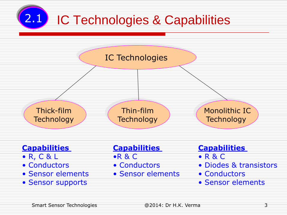
IC Technologies
Originally developed for producing micro-electronic
components and circuits
If sensor is an electrical or electronic device (e.g.
piezo-resistive strain gauge or P-N junction
temperature sensor), then the complete sensor can
be produced using IC technologies alone.
Micromachining Technologies
Originally developed for producing micro-mechanical
components and systems
Used only for producing sensing elements in the form
of a micro-mechanical structure or a micro-electro-
mechanical system (MEMS).
Smart Sensor Technologies @2014: Dr H.K. Verma
3
IC Technologies & Capabilities
Capabilities • R, C & L • Conductors • Sensor elements • Sensor supports
Capabilities •R & C • Conductors • Sensor elements
Capabilities • R & C • Diodes & transistors • Conductors • Sensor elements
Thick-film Technology
Thin-film Technology
Monolithic IC Technology
IC Technologies
2.1
Smart Sensor Technologies @2014: Dr H.K. Verma
4
Thick-Film Technology
Process : Materials: Paste :
Print Dry Fire Trim
+ Substrate Paste or Ink
Suspended particles of selected material
Dispersed in an organic solvent
Glass frit
2.2
+
+
Smart Sensor Technologies @2014: Dr H.K. Verma
Finish
+ Printing screen

5
Thick-Film Technology …………
Conductive For interconnections & small inductances
For resistances and sensors
For capacitors and some sensors
For some sensors and sensor supports
Particle Materials
Resistive
Dielectric
Other materials
Smart Sensor Technologies @2014: Dr H.K. Verma
6
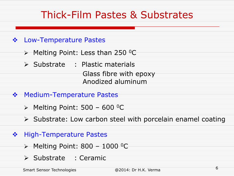
Thick-Film Pastes & Substrates
Low-Temperature Pastes
Melting Point: Less than 250 0C
Substrate : Plastic materials
Glass fibre with epoxy Anodized aluminum
Medium-Temperature Pastes
Melting Point: 500 – 600 0C
Substrate: Low carbon steel with porcelain enamel coating
High-Temperature Pastes
Melting Point: 800 – 1000 0C
Substrate : Ceramic
Smart Sensor Technologies @2014: Dr H.K. Verma

7
Thick-Film Process
Take substrate
Take printing screen & paste
Print as thick film on substrate
Dry the printed film at 1500 C
Fire on conveyer-belt furnance
Thick-film components ready
Trim components
Add IC chips
Repeat with another paste and printing screen until all films are deposited
Smart Sensor is ready
Screen printing Comp. width = 10-200 m Comp. thickness=10-25 m
Removes the organic solvent
By abrasion or laser vaporization Tolerance = 0.2–0.5 %
Tolerance = 10–20%
Metal powder sinters and glass frit melts thereby bonding the film to the substrate
Thick-Film Technology …………
Next
Smart Sensor Technologies @2014: Dr H.K. Verma
8
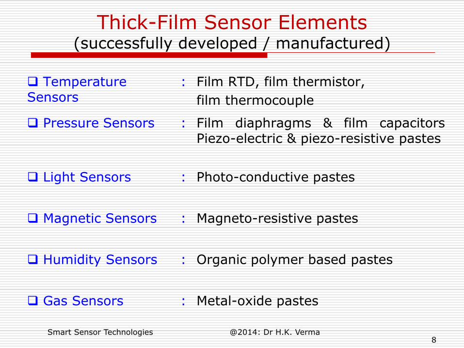
Thick-Film Sensor Elements (successfully developed / manufactured)
Temperature Sensors
: Film RTD, film thermistor,
film thermocouple
Pressure Sensors : Film diaphragms & film capacitors Piezo-electric & piezo-resistive pastes
Light Sensors
: Photo-conductive pastes
Magnetic Sensors : Magneto-resistive pastes
Humidity Sensors : Organic polymer based pastes
Gas Sensors : Metal-oxide pastes
Smart Sensor Technologies @2014: Dr H.K. Verma
9
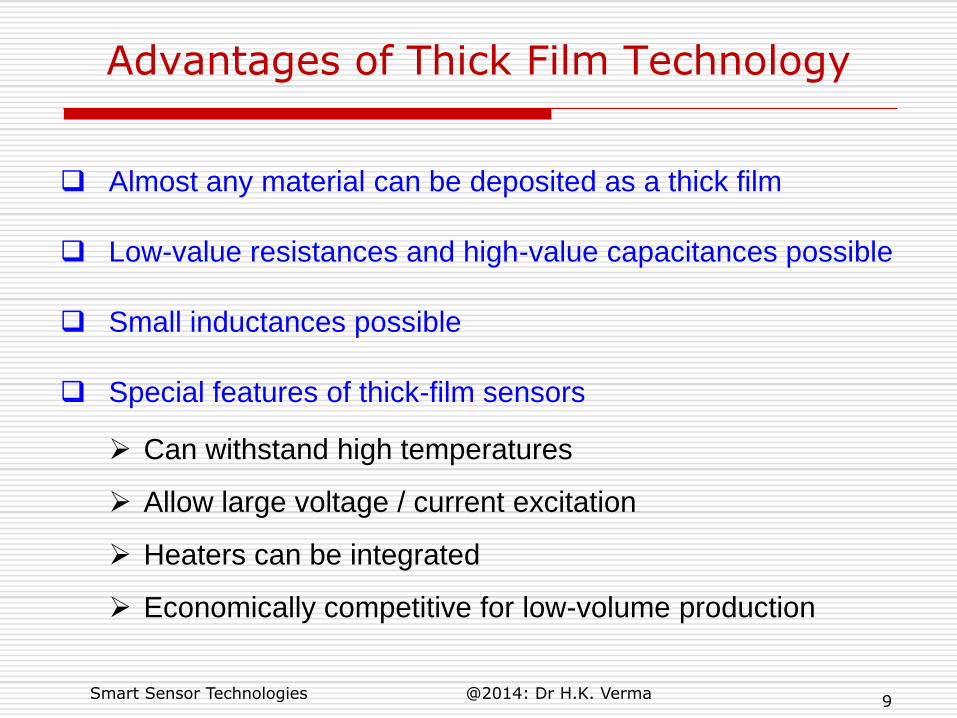
Advantages of Thick Film Technology
Almost any material can be deposited as a thick film
Low-value resistances and high-value capacitances possible
Small inductances possible
Special features of thick-film sensors
Can withstand high temperatures
Allow large voltage / current excitation
Heaters can be integrated
Economically competitive for low-volume production
Smart Sensor Technologies @2014: Dr H.K. Verma
10
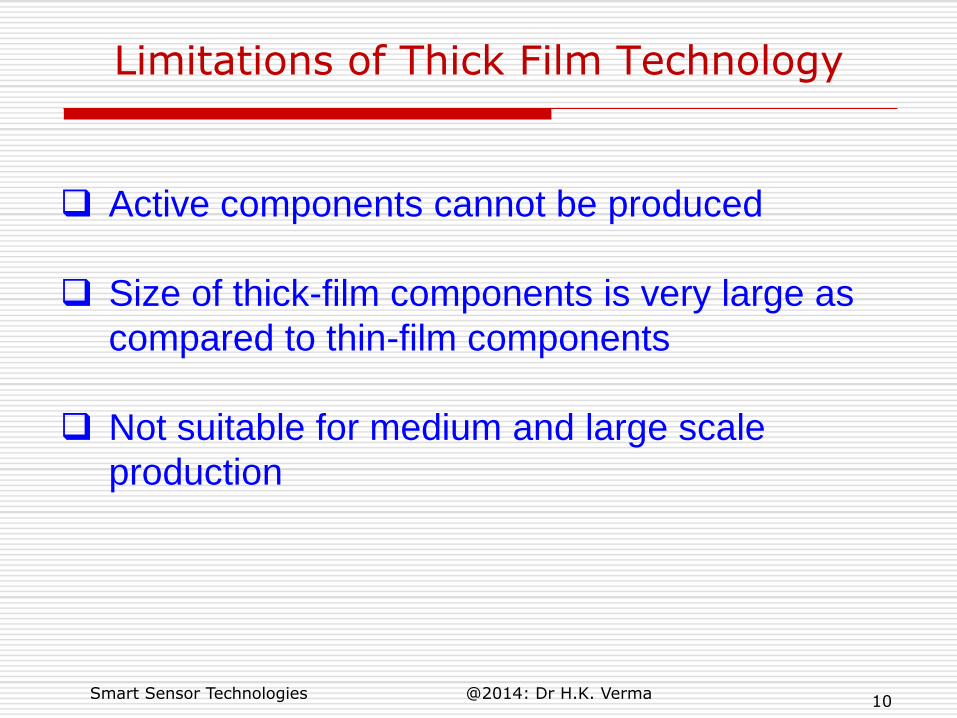
Limitations of Thick Film Technology
Active components cannot be produced
Size of thick-film components is very large as
compared to thin-film components
Not suitable for medium and large scale
production
Smart Sensor Technologies @2014: Dr H.K. Verma
11
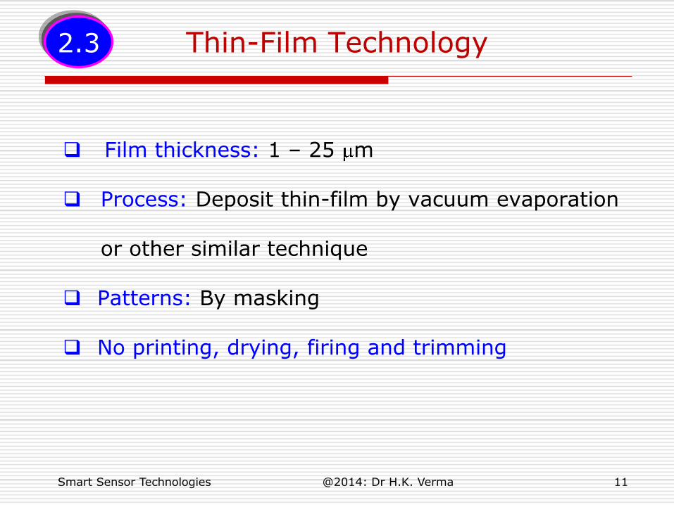
Thin-Film Technology
Film thickness: 1 – 25 m
Process: Deposit thin-film by vacuum evaporation
or other similar technique
Patterns: By masking
No printing, drying, firing and trimming
2.3
Smart Sensor Technologies @2014: Dr H.K. Verma
12
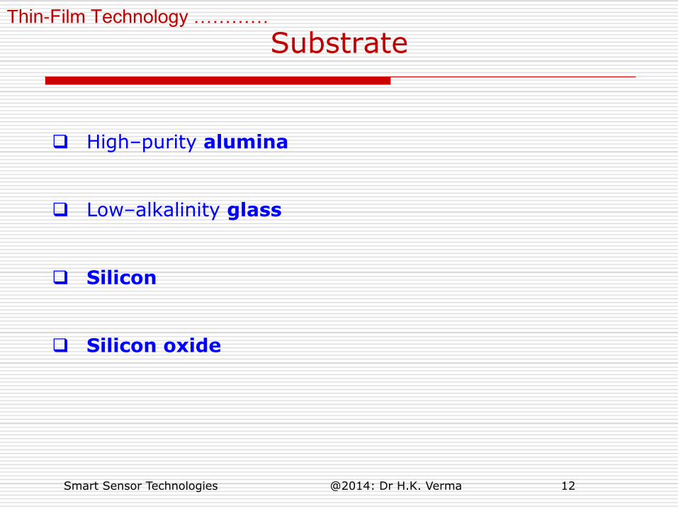
Substrate Thin-Film Technology …………
High–purity alumina
Low–alkalinity glass
Silicon
Silicon oxide
Smart Sensor Technologies @2014: Dr H.K. Verma
13
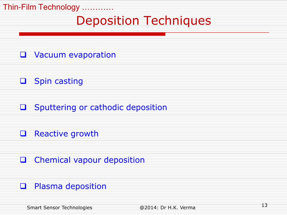
Deposition Techniques
Thin-Film Technology …………
Vacuum evaporation
Spin casting
Sputtering or cathodic deposition
Reactive growth
Chemical vapour deposition
Plasma deposition
Smart Sensor Technologies @2014: Dr H.K. Verma
14
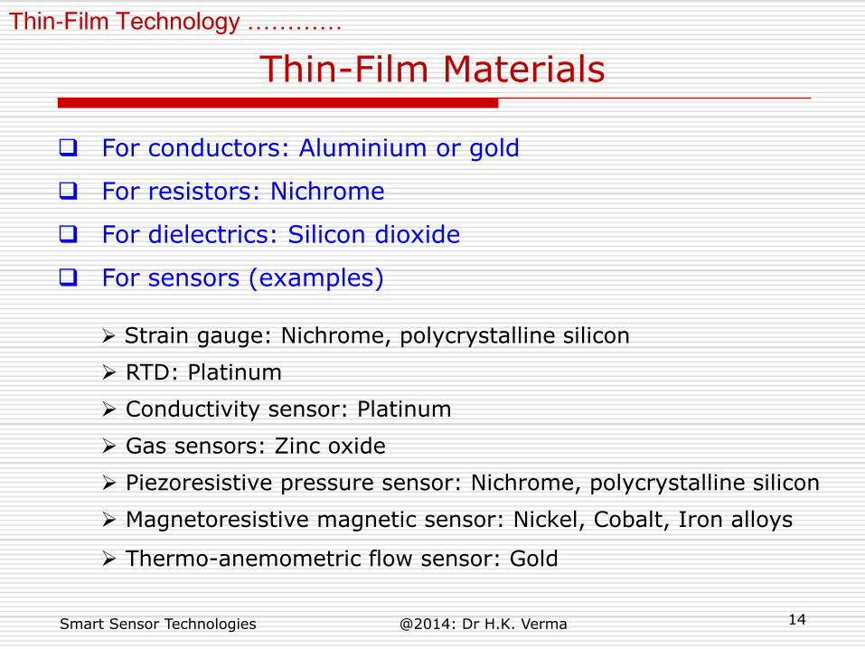
Thin-Film Materials
Thin-Film Technology …………
For conductors: Aluminium or gold
For resistors: Nichrome
For dielectrics: Silicon dioxide
For sensors (examples)
Strain gauge: Nichrome, polycrystalline silicon
RTD: Platinum
Conductivity sensor: Platinum
Gas sensors: Zinc oxide
Piezoresistive pressure sensor: Nichrome, polycrystalline silicon
Magnetoresistive magnetic sensor: Nickel, Cobalt, Iron alloys
Thermo-anemometric flow sensor: Gold
Smart Sensor Technologies @2014: Dr H.K. Verma
14
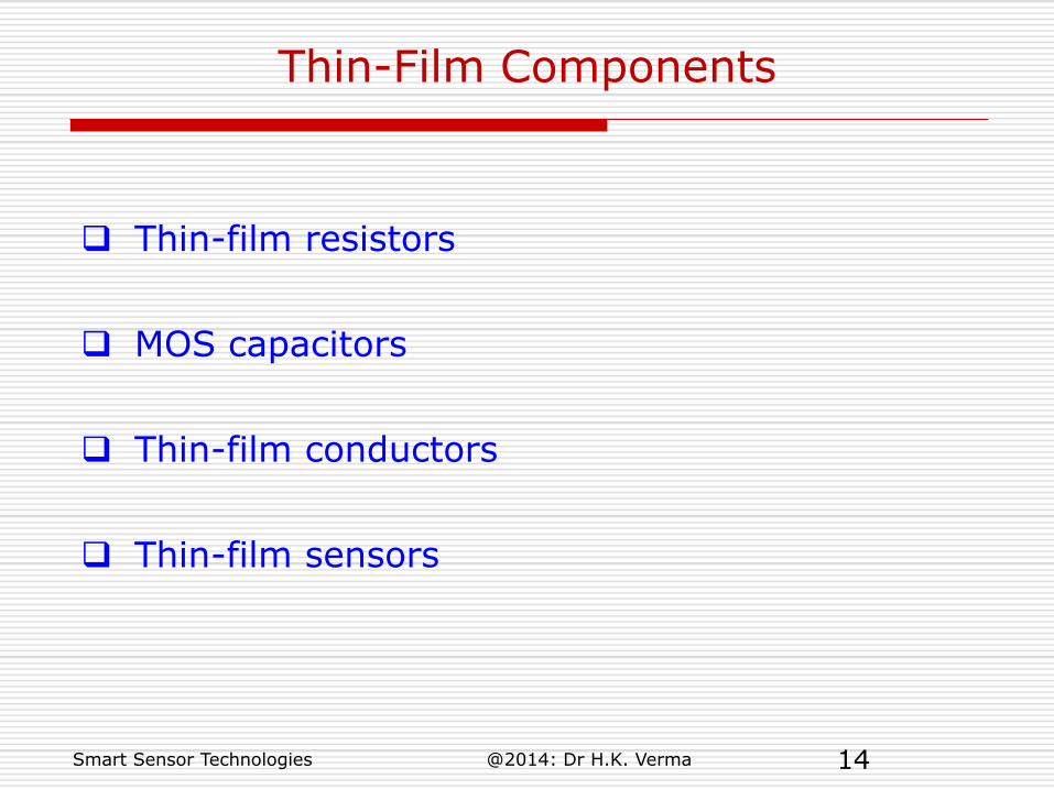
Thin-Film Components
Thin-film resistors
MOS capacitors
Thin-film conductors
Thin-film sensors
Smart Sensor Technologies @2014: Dr H.K. Verma

16
Advantages of Thin-Film Technology
Almost any metal can be deposited as thin film Miniaturization Suitable for adding resistances, capacitances and
sensors to monolithic IC Suitable for low and medium volume production
Smart Sensor Technologies @2014: Dr H.K. Verma
17
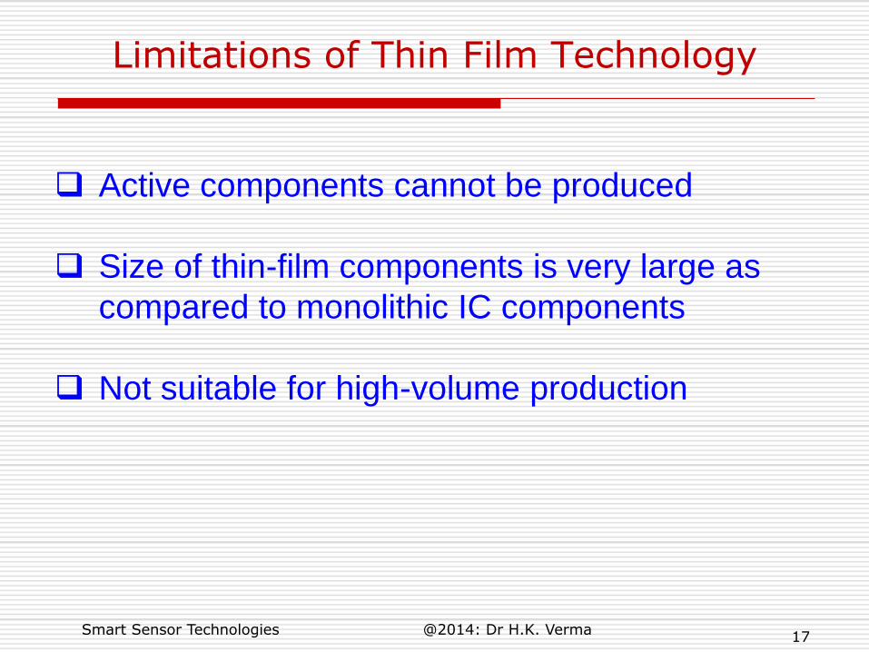
Limitations of Thin Film Technology
Active components cannot be produced
Size of thin-film components is very large as
compared to monolithic IC components
Not suitable for high-volume production
Smart Sensor Technologies @2014: Dr H.K. Verma
18
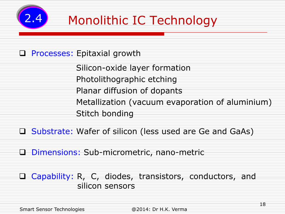
Monolithic IC Technology
Processes: Epitaxial growth
Silicon-oxide layer formation
Photolithographic etching
Planar diffusion of dopants
Metallization (vacuum evaporation of aluminium)
Stitch bonding
Substrate: Wafer of silicon (less used are Ge and GaAs)
Dimensions: Sub-micrometric, nano-metric
Capability: R, C, diodes, transistors, conductors, and silicon sensors
2.4
Smart Sensor Technologies @2014: Dr H.K. Verma
19
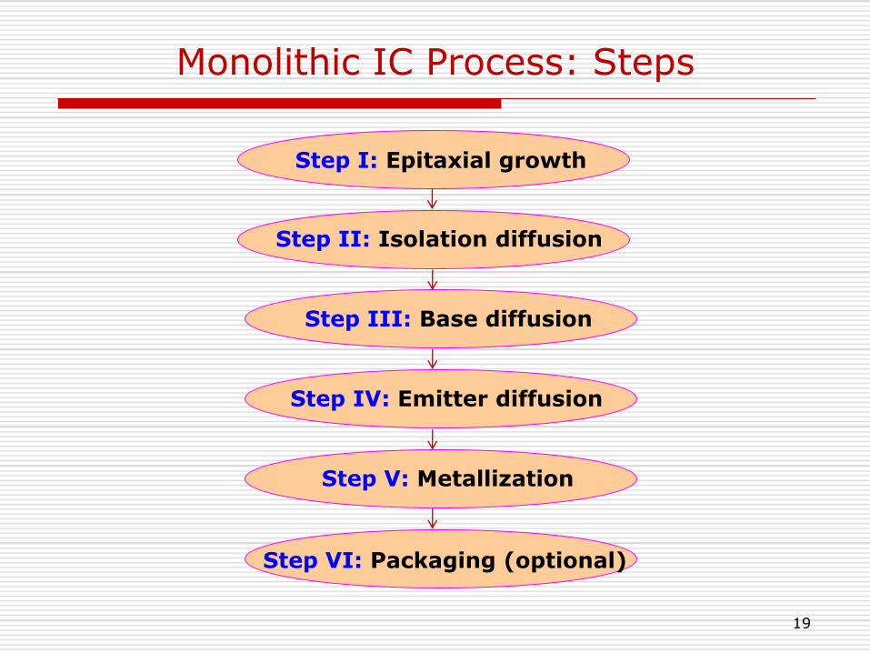
Monolithic IC Process: Steps
Step I: Epitaxial growth
Step II: Isolation diffusion
Step III: Base diffusion
Step IV: Emitter diffusion
Step V: Metallization
Step VI: Packaging (optional)
20
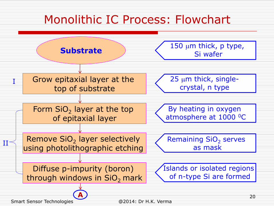
Monolithic IC Process: Flowchart
Substrate
Grow epitaxial layer at the top of substrate
Form SiO2 layer at the top of epitaxial layer
Remove SiO2 layer selectively using photolithographic etching
Diffuse p-impurity (boron) through windows in SiO2 mark
150 m thick, p type, Si wafer
25 m thick, single- crystal, n type
By heating in oxygen atmosphere at 1000 0C
Remaining SiO2 serves as mask
Islands or isolated regions of n-type Si are formed
II
I
A Smart Sensor Technologies @2014: Dr H.K. Verma

21
Monolithic IC Process: Flowchart (contd…)
Form second SiO2 layer at the top
Open second set of windows in SiO2 layer (mask)
Diffuse p-impurity through openings in mask
Form third SiO2 layer at the top
III
A
Open third set of windows in SiO2 layer (mask)
Diffuse n-impurity phosphorus through openings in mask
B
IV
The regions are: base of transistors,
anode of diodes, resistances
The regions are: emitter of transistors,
cathode of diodes, contact regions
(Contd…)
Smart Sensor Technologies @2014: Dr H.K. Verma
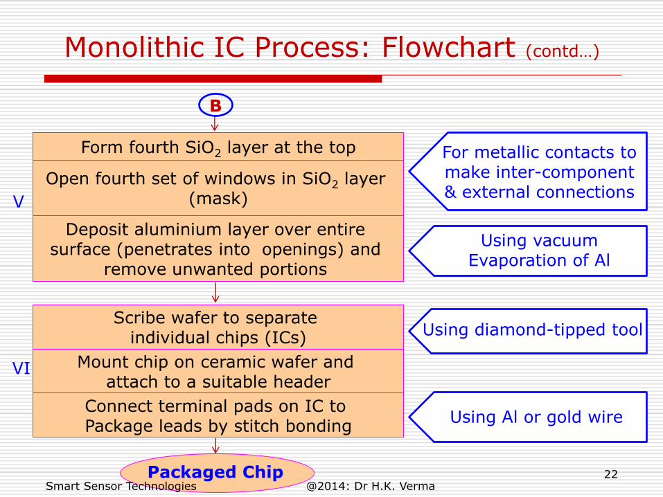
Monolithic IC Process: Flowchart (contd…)
Form fourth SiO2 layer at the top
Open fourth set of windows in SiO2 layer (mask)
Deposit aluminium layer over entire surface (penetrates into openings) and
remove unwanted portions
V
B
Scribe wafer to separate individual chips (ICs)
Mount chip on ceramic wafer and attach to a suitable header
Connect terminal pads on IC to Package leads by stitch bonding
VI
Packaged Chip
For metallic contacts to make inter-component & external connections
Using vacuum Evaporation of Al
Using diamond-tipped tool
Using Al or gold wire
22 Smart Sensor Technologies @2014: Dr H.K. Verma
23
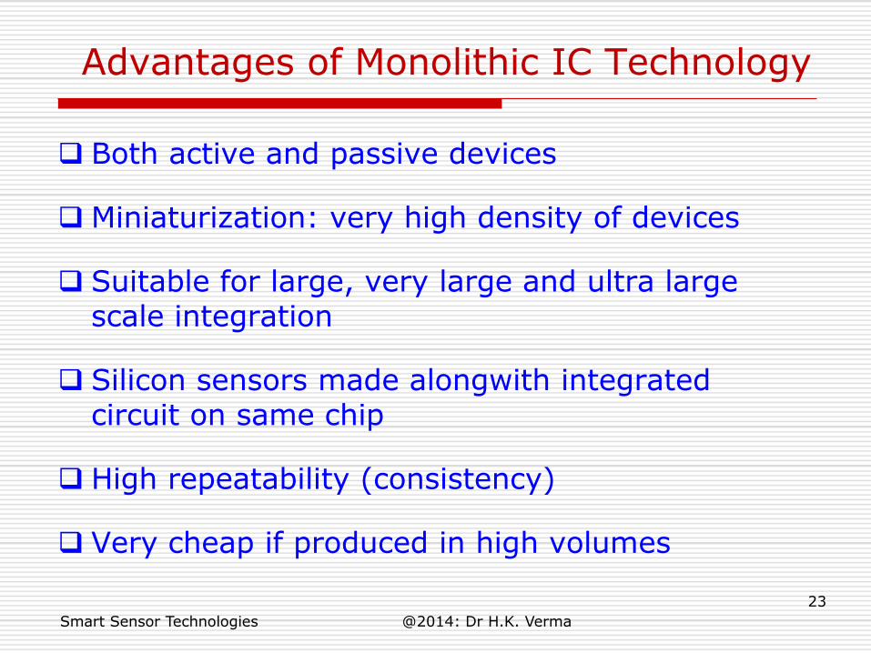
Advantages of Monolithic IC Technology
Both active and passive devices
Miniaturization: very high density of devices
Suitable for large, very large and ultra large scale integration
Silicon sensors made alongwith integrated circuit on same chip
High repeatability (consistency)
Very cheap if produced in high volumes
Smart Sensor Technologies @2014: Dr H.K. Verma

24
Limitations of Monolithic IC Technology
Sensors of silicon only
Resistances in medium-range only
Resistances have large temperature coefficient
Capacitors of small values only
Capacitors have some shortcomings
Too expensive for low-volume production
Smart Sensor Technologies @2014: Dr H.K. Verma
25
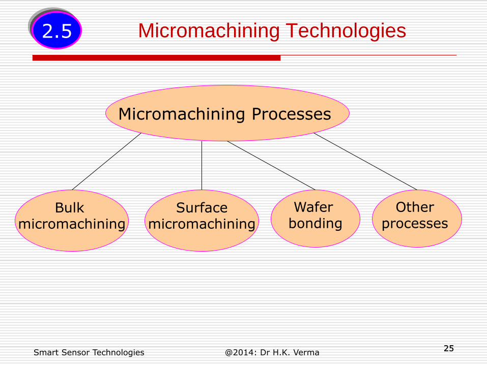
Micromachining Technologies
25
Micromachining Processes
Bulk micromachining
Surface micromachining
Wafer bonding
Other processes
2.5
Smart Sensor Technologies @2014: Dr H.K. Verma

26
Bulk Micromachining
Significant amounts of material are removed by chemical etching from relatively thick substrate
Substrate is usually silicon crystal; sometimes glass, quartz, germanium or gallium arsenide is used
Substrate (wafer) is etched on single side or both sides
Etching done with masks and etchants solutions
Masking by photolithographic etching technique
Etching processes:
a) Isotropic etching
b) Anistropic etching
Smart Sensor Technologies @2014: Dr H.K. Verma
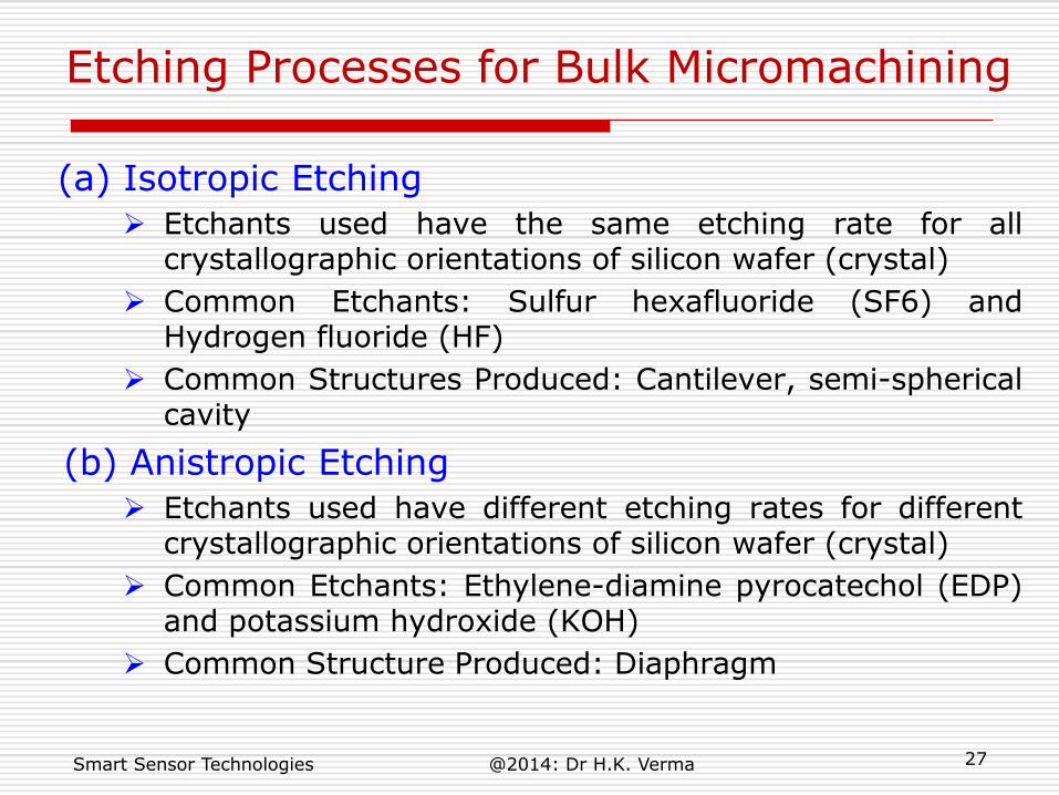
27
Etching Processes for Bulk Micromachining
(a) Isotropic Etching
Etchants used have the same etching rate for all crystallographic orientations of silicon wafer (crystal)
Common Etchants: Sulfur hexafluoride (SF6) and Hydrogen fluoride (HF)
Common Structures Produced: Cantilever, semi-spherical cavity
(b) Anistropic Etching
Etchants used have different etching rates for different crystallographic orientations of silicon wafer (crystal)
Common Etchants: Ethylene-diamine pyrocatechol (EDP) and potassium hydroxide (KOH)
Common Structure Produced: Diaphragm
Smart Sensor Technologies @2014: Dr H.K. Verma
28
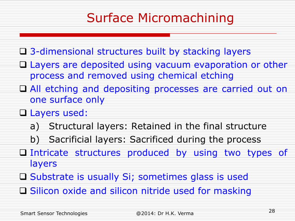
Surface Micromachining
3-dimensional structures built by stacking layers
Layers are deposited using vacuum evaporation or other process and removed using chemical etching
All etching and depositing processes are carried out on one surface only
Layers used:
a) Structural layers: Retained in the final structure
b) Sacrificial layers: Sacrificed during the process
Intricate structures produced by using two types of layers
Substrate is usually Si; sometimes glass is used
Silicon oxide and silicon nitride used for masking
Smart Sensor Technologies @2014: Dr H.K. Verma
29
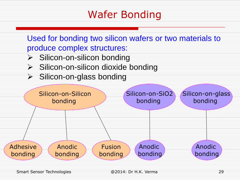
Wafer Bonding
Silicon-on-Silicon bonding
Silicon-on-glass bonding
Anodic bonding
Fusion bonding
Anodic bonding
Adhesive bonding
Smart Sensor Technologies @2014: Dr H.K. Verma
Used for bonding two silicon wafers or two materials to
produce complex structures:
Silicon-on-silicon bonding
Silicon-on-silicon dioxide bonding
Silicon-on-glass bonding
Silicon-on-SiO2 bonding
Anodic bonding
30
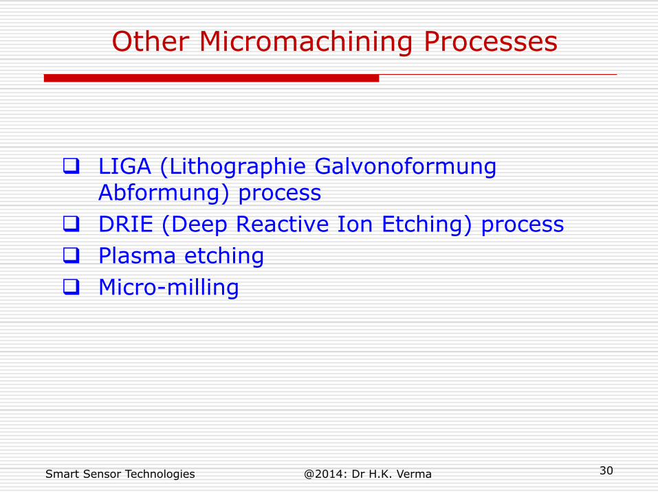
Other Micromachining Processes
LIGA (Lithographie Galvonoformung Abformung) process
DRIE (Deep Reactive Ion Etching) process
Plasma etching
Micro-milling
Smart Sensor Technologies @2014: Dr H.K. Verma