Lithography Etching Etching transfers the pattern from the ...glennc/e495/e495l5o.pdfLithography...
32
Lithography Etching • Etching transfers the pattern from the resist to the wafer layer • Resist protects pattern area • Etch removes unwanted material to define pattern Etching Definitions • Isotropic Etching: same in all direction • Anisotropic Etching: direction sensitive • Selectivity: etch rate difference between 2 materials • Need strong selectivity from masking material (eg. photoresist) • Also good selectivity for other layers below one being etch
Transcript of Lithography Etching Etching transfers the pattern from the ...glennc/e495/e495l5o.pdfLithography...

Lithography Etching • Etching transfers the pattern from the resist to the wafer layer • Resist protects pattern area • Etch removes unwanted material to define pattern Etching Definitions • Isotropic Etching: same in all direction • Anisotropic Etching: direction sensitive • Selectivity: etch rate difference between 2 materials • Need strong selectivity from masking material (eg. photoresist) • Also good selectivity for other layers below one being etch

Two Major types of etching • Wet Etching: Liquid acids/bases dissolves layer create pattern • Eg HF etches away the unprotected glass oxide • Most common for simple patterning >3 microns • Problem is isotropic etch – etches both down and to the side • Quick, cheap and fast • Dry Etching: using plasma or gases (2 types) • Plasma etching (PE) • Reactive Ion Etching (RIE) • Used for advanced etching typically < 2 microns • Tends to be anisotropic – less side etch • Also for better differentiation between layers

Basic Wet Etch Process • Diffusion of reactant to surface • Surface Reaction (absorption, reaction, desorption) • Diffusion of products from surface • This same cycle also applies to Dry Etching • The slowest of these limits the etching process

Rate Limiting Step • Rate limiting: slowest step which limits the process • Diffusion limited: reactant/product diffusion controlled • How fast reactant (or product) can get to the surface • Thus very agitation sensitive • Activation limited: surface reaction controlled • Reaction rate is usually Temperature sensitive
−=
KT
ERrate Aexp0
R0 = Rate constant (depends on reactant density) EA = Activation energy (in eV) T = Temperature (Kelvin) K = Boltzman's constant: 1.38 x 10²³ J/K = 8.62 x 10⁵ eV/K • Called Arrhenius behavior • Often plot against 1000/T for x axis and log rate on y

Typical Wet Etching Process • Etch proceeds both vertically and horizontally • Undercutting: material removed under the mask • At etch end has undercut edges • Etch proceeds at slower rate for etch stop material • Long overetch creates significant undercut
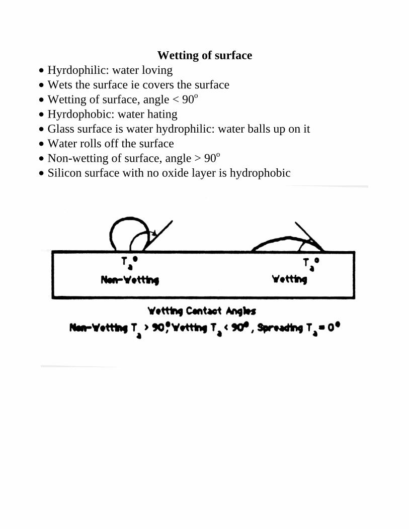
Wetting of surface • Hyrdophilic: water loving • Wets the surface ie covers the surface • Wetting of surface, angle < 90o • Hyrdophobic: water hating • Glass surface is water hydrophilic: water balls up on it • Water rolls off the surface • Non-wetting of surface, angle > 90o • Silicon surface with no oxide layer is hydrophobic

Common Chemicals used in Wet Etches • HF used for glass/silicon etch • Nitric Acid used in silicon etch • Phosphoric for Aluminum etch • Ammonium Fluoride in glass Buffered Oxide Etch • Ammonium Hydroxide in RCA Clean • Acetic Acid as buffer agent

Typical Wet Etchants • Many recipe’s possible for each materials • Important to note etch rate of material and other layers

Relative Chemical Purities • Super pure grade good enough for chemistry but not microfab • Must use electronic Grade

Chemical Impurities • Electronic Grade impurities not only small • Nill of deadly elements for devices eg Copper • Also low dopants (Boron, Arsinic)

Proper Wet Etching Station • Fume hood to remove gases • Moveable shield to protect workers

Professional Wet Etch Tub • Tub is full before wafers inserted (a) • Quick dump after etching for massive change (b) • Refilled with etchant (c)

Recirculating Wet Etch Tub • Tubs made of Teflon • Temperature controlled

Silicon Dioxide (Glass) • Glass - silicon dioxide: SiO2 • Used as a dielectric insulator between conductors • Also gate dielectric in Mosfets • Grown by Furnace oxidation (Wet/Dry) • Also by Chemical Vapour Deposition • Etched with HF containing solutions in reaction
SiO2 +6 HF → H2 + SiF6 + 2 H2O
• Depends on free fluorine
HF → H+ + F -
• Note the free hydrogen produced

Buffered Oxide Etch of Glass • Straight HF undercuts resist • Straight HF also diffuses through resist • Causes Adhesion loss on resist in long etches. • Since etch rate depends on free F- ions • Can stabilize F level with adding Ammonium Fluoride NH4F • Enhance etch rate and stabilize PH level • creates Buffered Oxide Etch (BOE) or Buffered HF (BHF) • Note increase in etch rate with temperature
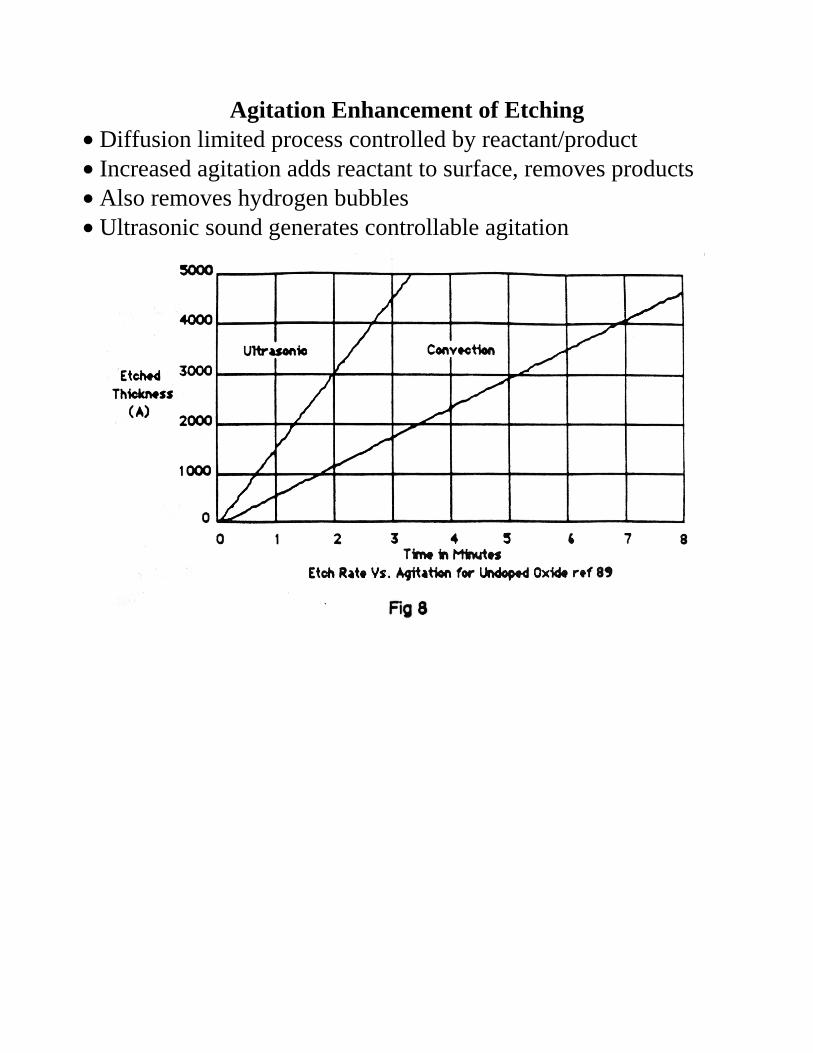
Agitation Enhancement of Etching • Diffusion limited process controlled by reactant/product • Increased agitation adds reactant to surface, removes products • Also removes hydrogen bubbles • Ultrasonic sound generates controllable agitation
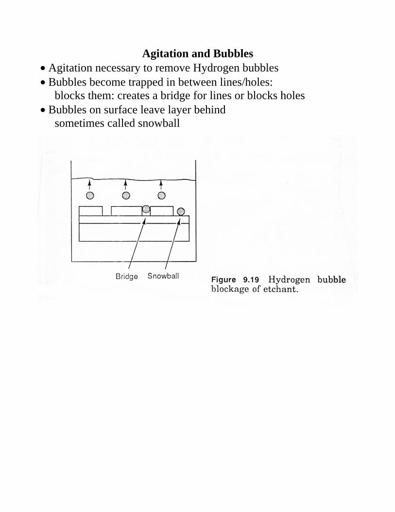
Agitation and Bubbles • Agitation necessary to remove Hydrogen bubbles • Bubbles become trapped in between lines/holes: blocks them: creates a bridge for lines or blocks holes • Bubbles on surface leave layer behind sometimes called snowball

Deposited Doped Oxides • Deposited oxides: high Boron, Phosphorous, Arsenic • Makes glass "soft" for other operations • Dopant can significantly affect etch rate • Boron lowers etch rate initially, then raises when enough B

Wet Etch Phosphosilicate Glass (PSG) • Glass with high phosphorus • used for layers between conductors • BOE etch rate increases with P content

Arsenic Doped Glass • Arsenic doping enhances etch rate • Lower density of Glass, faster etch rate

Etching and Undercutting • Perfect etching would be anisotropic • Would generate Vertical sidewalls (c) • Isotropic etch gets undercutting of resists removal of material under resist edge • Because etch rate differs across wafer Undercutting different across wafer

Isotropic Wet Etching and Feature Size • Isotropic etch proceeds at same rate "r" in all directions • Removes more at top edge than bottom • Thus create circular profile of etch with radius
R = rt
where t = time of etch (sec) r = etch rate (microns/sec) • Bottom of hole is flat, but edges curved • Incomplete etch: film layer not fully removed

Isotropic Wet Etching and Feature Size • Perfect etch then just clear bottom • Time of perfect etch is
r
z=τ
where z = film thickness • This generates minimum undercut • Side of lines measured at top/bottom • For perfect etch get line size at top
x = xL – 2rt
• But unevenness of etch over wafer means must have some overetch (eg 5-10%) at points • Overetch generates undercut at top: same formula • Significant undercut at bottom
( ) 222 zrtxx L −−=

Compensation for Undercut • Even with ideal isotropic etch get undercut • Bloat (expand) feature to compensate for undercut • Set bloat to compensate for difference across wafer • Resist is also etched, changing resist profile after etching • Ideally want perfect "etch stop": layer below that does not etch
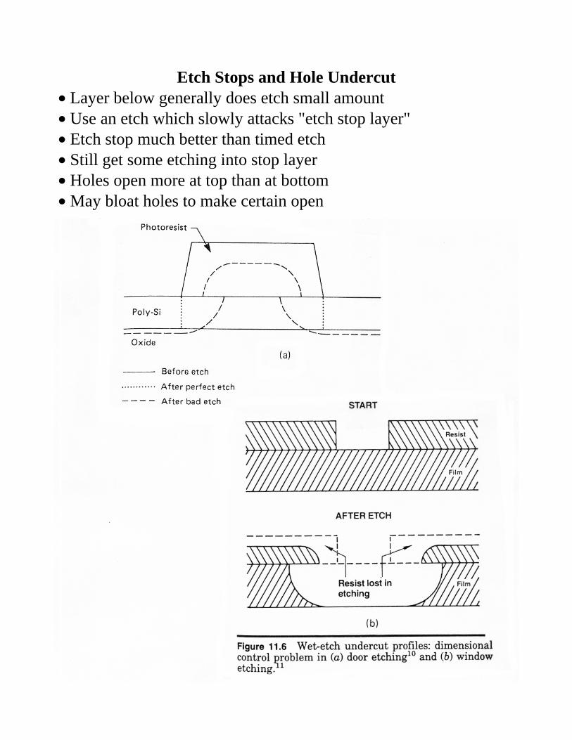
Etch Stops and Hole Undercut • Layer below generally does etch small amount • Use an etch which slowly attacks "etch stop layer" • Etch stop much better than timed etch • Still get some etching into stop layer • Holes open more at top than at bottom • May bloat holes to make certain open

Overetch Profile • Initial undercut nearly circular • As proceeds undercut get more vertical • Difference between top an bottom reduced

Sloped Sidewalls • Sometimes want sloped sidewalls: sloped edges • Easier for layers stepping over edge • As wet etch undercuts resist begins to lift off. • May deposit thin fast etch layer under mask • Generates shallow slope in undercut

Etching Bilayer Film • Sometimes put down two layers: fast and slow etch • Fast top layer undercuts with radius R
Rf = rft
• Slow lower layer matches upper at top • at bottom has its own etch radius
Rs = rst

Edge Residue and Etching • When film II steps over film I edge film II thicker at edge • More difficult to etch because thicker • Result often leave residue at edge • Isotropic wet etch does less of this.

Silicon Nitride • Nitride of silicon: Si3N4 • Used as a dielectric insulator between conductors • Also gate dielectric in Mosfets • Grown by Chemical Vapour Deposition • Usually non-stoichiometric (not proper composition ratio) SixN or SixNyHz • Also grow Silicon Oxynitrides SixOyNz • Very slow etching relative to oxide
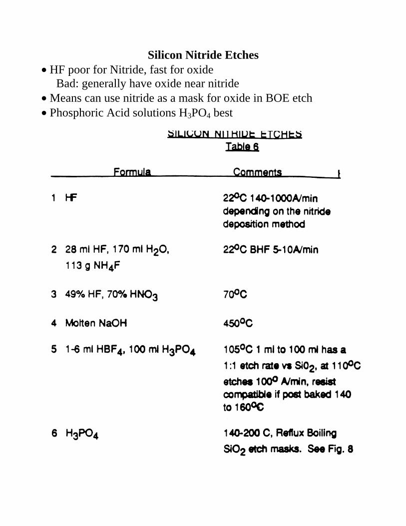
Silicon Nitride Etches • HF poor for Nitride, fast for oxide Bad: generally have oxide near nitride • Means can use nitride as a mask for oxide in BOE etch • Phosphoric Acid solutions H3PO4 best

Nitride Etch with Boiling Phosphoric Acid H3PO4 • Etches nitride mostly fast • Resist does lift during etch • Poor etch of oxide: • thus often use oxide as a mask for nitride