Sinusoidal Input Current Discontinuous Conduction Mode Control of the VIENNA Rectifier · ·...
14
© 2017 IEEE IEEE Transactions on Power Electronics, Vol. 32, No. 11, pp. 8800-8812, November 2017 Sinusoidal Input Current Discontinuous Conduction Mode Control of the VIENNA Rectifier M. Leibl, J. W. Kolar, J. Deuringer This material is published in order to provide access to research results of the Power Electronic Systems Laboratory / D-ITET / ETH Zurich. Internal or personal use of this material is permitted. However, permission to reprint/republish this material for advertising or promotional purposes or for creating new collective works for resale or redistribution must be obtained from the copyright holder. By choosing to view this document, you agree to all provisions of the copyright laws protecting it.
Transcript of Sinusoidal Input Current Discontinuous Conduction Mode Control of the VIENNA Rectifier · ·...

© 2017 IEEE
IEEE Transactions on Power Electronics, Vol. 32, No. 11, pp. 8800-8812, November 2017
Sinusoidal Input Current Discontinuous Conduction Mode Control of the VIENNA Rectifier
M. Leibl,J. W. Kolar,J. Deuringer
This material is published in order to provide access to research results of the Power Electronic Systems Laboratory / D-ITET / ETH Zurich. Internal or personal use of this material is permitted. However, permission to reprint/republish this material for advertising or promotional purposes or for creating new collective works for resale or redistribution must be obtained from the copyright holder. By choosing to view this document, you agree to all provisions of the copyright laws protecting it.

8800 IEEE TRANSACTIONS ON POWER ELECTRONICS, VOL. 32, NO. 11, NOVEMBER 2017
Sinusoidal Input Current Discontinuous ConductionMode Control of the VIENNA Rectifier
Michael Leibl, Member, IEEE, Johann W. Kolar, Fellow, IEEE, and Josef Deuringer
Abstract—During light load conditions unidirectional power fac-tor correction rectifiers, such as the VIENNA rectifier, enter dis-continuous conduction mode, causing the relationship between av-erage half-bridge voltage and duty cycle to become nonlinear andsynchronously sampled current measurements not equaling theswitching period average. Combined, these measurement and ac-tuation errors result in distorted input currents at light load ifno additional measures are taken. This work presents a controlscheme that leads to low total harmonic distortion of the input cur-rents in discontinuous conduction mode without relying on currentmeasurements. The analytic expressions for the duty cycles and thethreshold between discontinuous and continuous conduction modeare derived, the capability of supplying asymmetric loads is investi-gated and the effect on the noise spectrum relevant for the electro-magnetic interference filter design is studied. Measurements of ef-ficiency, total harmonic distortion, and conducted electromagneticinterference in discontinuous and continuous conduction mode areobtained on a 65 kW prototype operating at 290 to 530 V line-to-line RMS mains voltage range and supplying 800 V dc outputvoltage. The prototype, which is optimized for pulse load applica-tions, achieves a power density of 9.56 kW/dm3 (157 W/in3) and97.2 % efficiency at full load using 650 V Si insulated gate bipolartransistor (IGBTs) with 28 kHz switching frequency.
Index Terms—AC-DC converter, discontinuous conductionmode, light load, pulse load, three-phase rectifier.
I. INTRODUCTION
M EDICAL X-ray system power supplies have to providehigh dc voltages of up to 150 kV to the X-ray tube.
Most of the power is dissipated as heat within the anode of thevacuum tube and only ≈ 1% of the power is actually emittedas Bremsstrahlung, which is used for diagnostic and also fortherapy purposes [1]. Since the vacuum tube only provides lim-ited heat transfer to the ambient, the average power that can besupplied to the tube is given by the maximum temperature of theanode and its thermal resistance to the ambient and it typicallyamounts to less than 1 kW. The peak power, however, is only lim-ited by the internal thermal resistance of the anode, which is typ-
Manuscript received September 22, 2016; accepted December 5, 2016. Dateof publication December 19, 2016; date of current version June 23, 2017.Recommended for publication by Associate Editor Richard Redl.
M. Leibl is with the Department of Information Technology and Elec-trical Engineering, ETH Zurich, Zurich 8092, Switzerland (e-mail: [email protected]).
J. W. Kolar is with the Department of Electrical Engineering, ETH Zurich,Zurich 8092, Switzerland (e-mail: [email protected]).
J. Deuringer is with the Clinical Products Division, Siemens HealthcareGmbH, Erlangen 91052, Germany (e-mail: [email protected]).
Color versions of one or more of the figures in this paper are available onlineat http://ieeexplore.ieee.org.
Digital Object Identifier 10.1109/TPEL.2016.2641502
ically a composite of tungsten and copper or molybdenum [2].Therefore, it can be considerably higher reaching values up to100 kW. The duration of such a full power pulse is limited by thetotal amount of energy, which can be stored in the thermal ca-pacitance of the anode at its maximum temperature, thus usuallyfull load pulses are limited to less than 10 s.
Therefore, power supplies of X-ray systems can be designedto take advantage of the relatively low average power. Also,due to the low amount of full load operating hours the primaryobjective is to reach lowest material cost instead of highest ef-ficiency, while maintaining high reliability despite the thermalcycling [3]. For this reasons nowadays X-ray power supplies areusing passive diode rectifiers supplying a dc voltage, which isdepending on the mains voltage. In order to deal with 400 and480 V mains voltages with 10% over- and 20% under-voltagetolerances, high-voltage generators connected to passive rec-tifiers, therefore, have to be able to cope with a wide inputvoltage range, while also providing a wide output voltage rangeof typically 100 to 150 kV at full power, limiting the over-all system performance. Furthermore, six pulse diode rectifiersexhibit considerable harmonic current emissions, which mayrequire additional low-frequency harmonic filtering dependingon the utility grid regulations [4].
To relieve the stress on the high-voltage generator and toincrease the input current quality an active rectifier shall be op-timized for a given pulsed load scenario of 65 kW peak powerfor up to 10 s with 1 kW average power. Because only uni-directional power flow is required, the three-level three-phaserectifier often referred to as VIENNA rectifier (VR), is wellsuited since it provides stable dc-link voltage and sinusoidal in-put currents. Compared to the two-level six-switch rectifier [5],the power semiconductors only need to block half of the dc-linkvoltage, which can be as low as the line-to-line peak voltage.Therefore, low switching loss 650 V insulated gate bipolar tran-sistor (IGBTs) in combination with low reverse recovery charge650 V free-wheeling diodes can be employed, which match thelow-cost, high-reliability design target. Due to the three-leveltopology, also the maximum voltage time product applied to theboost inductors is only half of the one of a two-level topology.Different circuit variants of the VR exist including the originalthree switch solution [6] and the T-type variant [7], however,the neutral point clamped (NPC) structure as shown in Fig. 1 ischosen since it includes only two semiconductors in the com-mutation loop, both subjected to only half the dc-link voltageand only two semiconductors in the current path of each phase.Additionally to the six free-wheeling diodes of the boost stages,
0885-8993 © 2016 IEEE. Personal use is permitted, but republication/redistribution requires IEEE permission.See http://www.ieee.org/publications standards/publications/rights/index.html for more information.
LEIBL et al.: SINUSOIDAL INPUT CURRENT DISCONTINUOUS CONDUCTION MODE CONTROL OF THE VIENNA RECTIFIER 8801
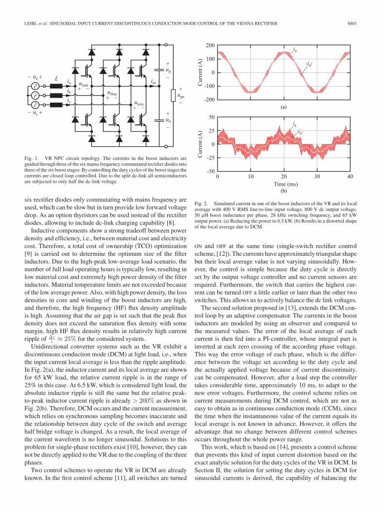
Fig. 1. VR NPC circuit topology. The currents in the boost inductors areguided through three of the six mains frequency commutated rectifier diodes intothree of the six boost stages. By controlling the duty cycles of the boost stages thecurrents are closed loop controlled. Due to the split dc-link all semiconductorsare subjected to only half the dc-link voltage.
six rectifier diodes only commutating with mains frequency areused, which can be slow but in turn provide low forward voltagedrop. As an option thyristors can be used instead of the rectifierdiodes, allowing to include dc-link charging capability [8].
Inductive components show a strong tradeoff between powerdensity and efficiency, i.e., between material cost and electricitycost. Therefore, a total cost of ownership (TCO) optimization[9] is carried out to determine the optimum size of the filterinductors. Due to the high-peak low-average load scenario, thenumber of full load operating hours is typically low, resulting inlow material cost and extremely high power density of the filterinductors. Material temperature limits are not exceeded becauseof the low average power. Also, with high power density, the lossdensities in core and winding of the boost inductors are high,and therefore, the high frequency (HF) flux density amplitudeis high. Assuming that the air gap is set such that the peak fluxdensity does not exceed the saturation flux density with somemargin, high HF flux density results in relatively high currentripple of Δ i
i ≈ 25% for the considered system.Unidirectional converter systems such as the VR exhibit a
discontinuous conduction mode (DCM) at light load, i.e., whenthe input current local average is less than the ripple amplitude.In Fig. 2(a), the inductor current and its local average are shownfor 65 kW load, the relative current ripple is in the range of25% in this case. At 6.5 kW, which is considered light load, theabsolute inductor ripple is still the same but the relative peak-to-peak inductor current ripple is already > 200% as shown inFig. 2(b). Therefore, DCM occurs and the current measurement,which relies on synchronous sampling becomes inaccurate andthe relationship between duty cycle of the switch and averagehalf bridge voltage is changed. As a result, the local average ofthe current waveform is no longer sinusoidal. Solutions to thisproblem for single-phase rectifiers exist [10], however, they cannot be directly applied to the VR due to the coupling of the threephases.
Two control schemes to operate the VR in DCM are alreadyknown. In the first control scheme [11], all switches are turned
Fig. 2. Simulated current in one of the boost inductors of the VR and its localaverage with 400 V RMS line-to-line input voltage, 800 V dc output voltage,50 µH boost inductance per phase, 28 kHz switching frequency, and 65 kWoutput power. (a) Reducing the power to 6.5 kW. (b) Results in a distorted shapeof the local average due to DCM.
ON and OFF at the same time (single-switch rectifier controlscheme, [12]). The currents have approximately triangular shapebut their local average value is not varying sinusoidally. How-ever, the control is simple because the duty cycle is directlyset by the output voltage controller and no current sensors arerequired. Furthermore, the switch that carries the highest cur-rent can be turned OFF a little earlier or later than the other twoswitches. This allows us to actively balance the dc link voltages.
The second solution proposed in [13], extends the DCM con-trol loop by an adaptive compensator. The currents in the boostinductors are modeled by using an observer and compared tothe measured values. The error of the local average of eachcurrent is then fed into a PI-controller, whose integral part isinverted at each zero crossing of the according phase voltage.This way the error voltage of each phase, which is the differ-ence between the voltage set according to the duty cycle andthe actually applied voltage because of current discontinuity,can be compensated. However, after a load step the controllertakes considerable time, approximately 10 ms, to adapt to thenew error voltages. Furthermore, the control scheme relies oncurrent measurements during DCM control, which are not aseasy to obtain as in continuous conduction mode (CCM), sincethe time when the instantaneous value of the current equals itslocal average is not known in advance. However, it offers theadvantage that no change between different control schemesoccurs throughout the whole power range.
This work, which is based on [14], presents a control schemethat prevents this kind of input current distortion based on theexact analytic solution for the duty cycles of the VR in DCM. InSection II, the solution for setting the duty cycles in DCM forsinusoidal currents is derived, the capability of balancing the

8802 IEEE TRANSACTIONS ON POWER ELECTRONICS, VOL. 32, NO. 11, NOVEMBER 2017
Fig. 3. Boost inductor currents during one switching period in DCM withsynchronously operated switches while ua > 0 > ub > uc (a) and space vectorrepresentation of the same situation (b).
dc-link voltages and supplying asymmetric loads (unequalpower drawn from the partial output voltages up and un ) is in-vestigated, the threshold to CCM is derived and the effect on theconducted electromagnetic interference (EMI) noise emissionis studied. In Section III, experiments on a hardware prototypeare presented that confirm the feasibility of the approach includ-ing control performance during load steps and efficiency, totalharmonic distortion (THD) and EMI measurements.
II. ANALYSIS
Aiming for a better understanding of the behavior of the VRin DCM space vector representations for voltages and currentscan be used [12]. With a = exp(j 2π
3 ) the mains voltages aretransformed into the space vector
u = uα + juβ =23(ua + aub + a2uc) (1)
the rectifier input voltages into the space vector
ur = urα + jurβ =23(uram + aurbm + a2urcm) (2)
and the boost inductor currents into the space vector
i = iα + jiβ =23(ia + aib + a2ic). (3)
For the following considerations a switching period at a mainsvoltage angle of ϕ = 10◦ of a symmetric three-phase systemwith ua = u cos(ϕ), ub = u cos(ϕ − 2π
3 ), uc = u cos(ϕ − 4π3 )
is considered. The values of the mains voltages, which are as-sumed to be constant during the switching period, therefore,satisfy the condition ua > 0 > ub > uc . It is also assumed thatat the beginning of the switching period Ts = 1
fs, the boost
inductor currents are zero.
A. Synchronous Switching DCM
One option, to control the VR in DCM, is to operate allswitches synchronously, i.e., to turn them ON and OFF at thesame time setting the duty cycle such that the required poweris transferred into the dc-link. However, this operating principleresults in nonsinusoidal input currents as can be easily shown byusing space vector representation. After turning ON all switchesat t = 0, each current is rising at a rate proportional to its ac-cording phase voltage as shown in interval 1 in Fig. 3(a). The
Fig. 4. Simulated boost inductor current of one phase and its local averagevalue in DCM with synchronously operated switches. Operating condition andparameters used for the simulation: u =
√2· 230 V, Upn = 800 V, P = 13 kW,
fs = 28 kHz, L = 50 µH.
space vector representation of this interval shown in Fig. 3(b)reveals that according to
di
dt=
1L
(u − ur) (4)
the current space vector is moving along the indicated trajectory1 in the direction of the mains voltage space vector, since the
rectifier voltage space vector ur(111) is zero. After turning OFF
all switches at the same time, the phase currents commutate tothe free-wheeling diodes and thus during this interval 3 allphase currents are decreasing. The voltage space vector appliedto the boost inductors now is the difference between the recti-fier voltage space vector ur(000), which is applied during thisswitching state and the mains voltage space vector. The boostinductor current space vector, therefore, moves along the trajec-tory 3 during this state. As soon as the phase current with the
smallest absolute value (ib ) reaches zero, state 4 is entered.Now, the difference between the rectifier voltage space vector3 projected to the line ib = 0 and the mains voltage space vec-
tor is applied to the boost inductors. The boost inductor currentspace vector moves along the line ib = 0 until it reaches the ori-gin where it remains until the end of the switching period. Thisinvestigation shows that the local average of the boost induc-tor current with synchronous switching is located somewherewithin the triangle 1 - 3 - 4 , which is aligned with the mainsvoltage space vector with one side. Therefore, the local aver-age of the boost inductor current space vector is generally notin phase with the mains voltage space vector. Since the phaseshift between the mains voltage space vector and the local aver-age of the boost inductor current space vector varies throughoutthe mains period, taking positive and negative values, a nonsinu-soidal shape of the input current is observed with synchronouslycontrolled switches. This is confirmed by the simulated wave-form shown in Fig. 4.
B. Proposed Sinusoidal Current DCM Pattern A
In order to achieve sinusoidal input currents, the phase shiftbetween the local average of the boost inductor current spacevector and the mains voltage has to be constant throughout themains period. Achieving zero phase shift, i.e., resistive mainsbehavior, is intended in the following. For zero phase shift in theconsidered example an additional voltage space vector has to be

LEIBL et al.: SINUSOIDAL INPUT CURRENT DISCONTINUOUS CONDUCTION MODE CONTROL OF THE VIENNA RECTIFIER 8803
Fig. 5. Boost inductor currents during one switching period in DCM employ-
ing switching state 2A while ua > 0 > ub > uc . (a) Space vector represen-
tation of the same situation. (b) The duration of the switching state 2A ischosen such that the phase shift between mains voltage space vector and boostinductor current space vector is zero.
Fig. 6. Simulated boost inductor current of one phase, its local average value,and the local average value of the midpoint current in DCM employing switching
state 2A to reach resistive mains behavior. Operating condition and parameters
used for the simulation: u =√
2· 230 V, Upn = 800 V, P = 13 kW, fs =28 kHz, L = 50 µH.
applied as shown in Fig. 5(b). Turning off the switch of phase cearlier than the others, inserts the state 2A with the accordingvoltage space vector that shifts the boost inductor current spacevector into the appropriate direction to eliminate the phase shiftbetween mains voltage and boost inductor current. The phasecurrent waveforms during one switching period applying to thissituation are shown in Fig. 5(a) and it can be observed that duringstate 2A the absolute value of the current of the phase with thesmallest absolute voltage increases. At the same time a currentim is injected into the dc-link midpoint with opposite sign asthe phase voltage with smallest absolute value. By adjusting theduration of state 2A such that zero phase shift is maintainedthroughout the mains period the simulated waveform of theboost inductor current of one phase shown in Fig. 6 is obtained.The local average of the boost inductor current is sinusoidal andit can be observed that the local average of the midpoint currentvaries with three times the mains frequency and contains nodc-component.
C. Proposed Sinusoidal Current DCM Pattern B
Although when using the switching pattern described inSection II-B, the generated midpoint current contains no dc-component, it is desired to be able to provide a small dc mid-point current to counteract asymmetric leakage currents or smallasymmetric loads connected to the output that would otherwisecause unbalanced dc-link voltages. Using the switching state
Fig. 7. Boost inductor currents during one switching period in DCM employ-
ing switching state 2B while ua > 0 > ub > uc . (a) Space vector represen-
tation of the same situation. (b) Duration of the switching state 2B is chosensuch that the phase shift between mains voltage space vector and boost inductorcurrent space vector is zero.
Fig. 8. Simulated boost inductor current of one phase, its local average value,and the local average value of the midpoint current in DCM employing switching
state 2B to reach resistive mains behavior. Operating condition and parameters
used for the simulation: u =√
2· 230 V, Upn = 800 V, P = 13 kW, fs =28 kHz, L = 50 µH.
010 in the aforementioned example as shown in Fig. 7 allowsexactly that. By leaving the switch of the phase with the smallestabsolute voltage turned ON longer than the two others, switch-ing state 2B is inserted between states 1 and 3 . The spacevector diagram in Fig. 7(b) shows that this switching state alsoallows us to achieve zero phase shift between mains voltage andlocal average of the boost inductor current, if the duration ofthe state is chosen correctly. The current waveforms during oneswitching period [see Fig. 7(a)] reveal that the absolute valueof the current of the phase with the smallest absolute voltage isalso rising, as it is when state 2A is applied. However, since
the midpoint current during state 2B equals the current ofthe phase with the smallest absolute value of the voltage thedirection of the midpoint current during state 2B is opposite
to its direction during state 2A . If the duration of state 2Ais chosen correctly to eliminate the phase shift between mainsvoltage and boost inductor current throughout the mains period,the local average of the boost inductor current is also sinusoidalas shown in Fig. 8. By comparing Figs. 6 and 8, it is observedthat the local average of the midpoint current has opposite signin the two different switching patterns A and B.
D. Calculation of the Duty Cycles
In order to actually achieve sinusoidal currents by using theswitching patterns, described in Sections II-B and II-C, the

8804 IEEE TRANSACTIONS ON POWER ELECTRONICS, VOL. 32, NO. 11, NOVEMBER 2017
TABLE ISWITCHING STATES OF THE PROPOSED SINUSOIDAL CURRENT DCM CONTROL SCHEME, ASSUMING ua >0>ub >uc
durations of switching states 1 , 2A , and 2B have to beset correctly, depending on the amount of power to be trans-ferred, the values of the phase voltages, and the dc-link voltage.As shown in the following the required expressions can be foundanalytically. For each of the described five switching states, nthe equivalent circuit, the current change Δikn in each phasemains k and the duration Tn are given in Table I. Using theseequations the local average values of the currents in the boostinductors are calculated as
〈ik 〉 =12
(Δik1T1 + (Δik1 + Δik2x)T2x + (Δik1 + Δik2x
+Δik3)T3 + (Δik1 + Δik2x + Δik3 + Δik4)T4) fs
(5)
with x being either A or B. In order to obtain sinusoidal inputcurrents, the rectifier has to act like a symmetric three-phaseresistive load concerning the local current average values 〈ik 〉.Therefore, it is required that for each phase k the resistancerk = uk
〈ik 〉 is the same, i.e., rk = r. Assuming∑
k uk = 0 and∑
k ik = 0, this condition is guaranteed if the resistances of twophases are the same. Therefore, solving the equation
ua
〈ia〉 =ub
〈ib〉 (6)
with the local average values of the currents inserted from (5),yields the value of D2A or D2B (as defined in Table I) that isnecessary for resistive behavior, i.e., sinusoidal input currentsafter filtering switching frequency components. The value of D1follows by inserting the values D2A or D2B obtained from (6)
into any of the equations r = uk
〈ik 〉 for a required resistance r atthe mains side. In order to normalize the resistance r emulatedto the mains and the phase voltages, and in order to include the30◦ symmetry of the three phase system
D0 =
√fsL
r(7)
mmax =2 · max(|ua|, |ub|, |uc|)
Upn(8)
mmin =2 · min(|ua|, |ub|, |uc|)
Upn(9)
are introduced. Using these expressions the duty cycles forswitching pattern B are obtained as
D1B = D0√
2 − 2mmax + mmin (10)
D2B = D0√
2 − 3mmin − D1B . (11)
The expressions for the duty cycles for pattern A are providedin Appendix due to the complexity of the terms. Because of thata realization of the control scheme in hardware is only possibleby using look-up tables of the relative duty cycles d1A = D1 A
D0,
d2A = D2 AD0
and d1B = D1 BD0
, d2B = D2 BD0
. With the modulation
index M = 2uUp n
the relative duty cycles are shown in Fig. 9. Itis observed, that the functions are smooth and continuous, andtherefore, well suited for implementation using look-up tables.It is observed that for high values of the modulation index,the duty cycle functions (18,19,10,11) result in negative values.Numerical investigations show that all duty cycle values are
LEIBL et al.: SINUSOIDAL INPUT CURRENT DISCONTINUOUS CONDUCTION MODE CONTROL OF THE VIENNA RECTIFIER 8805
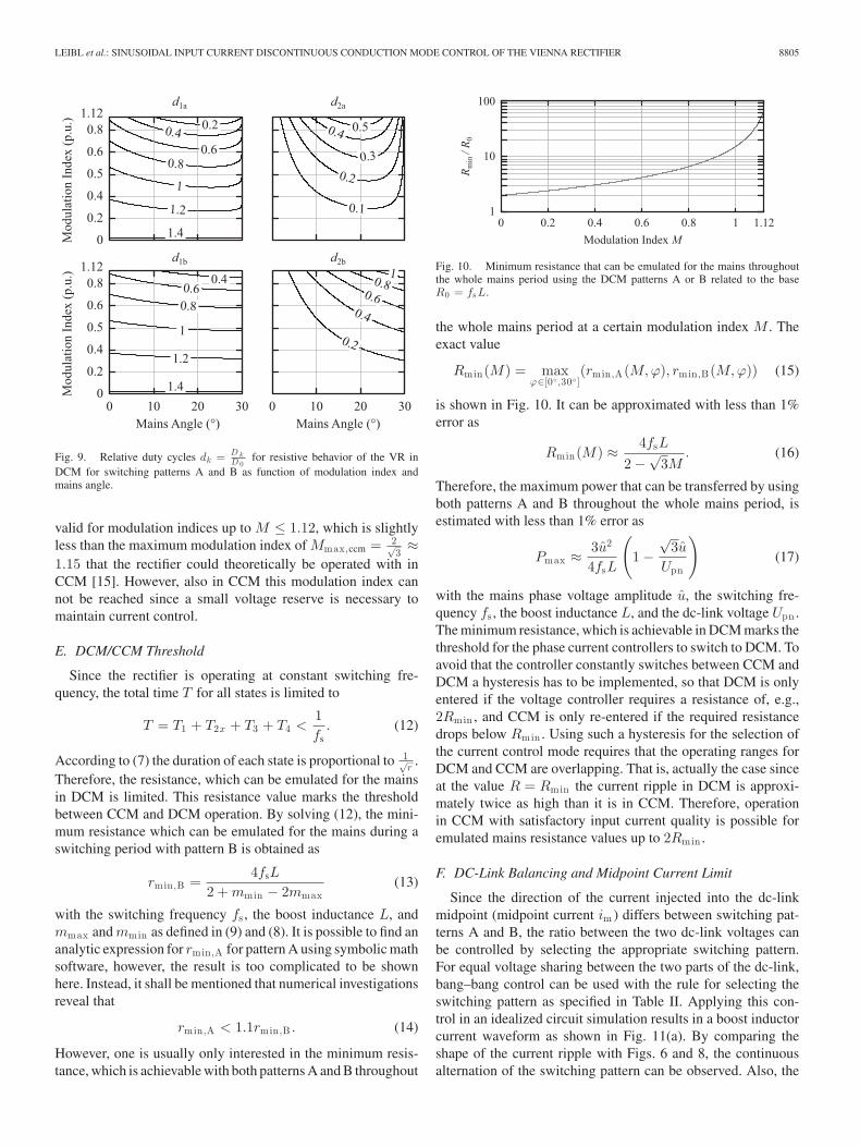
Fig. 9. Relative duty cycles dk = D kD 0
for resistive behavior of the VR inDCM for switching patterns A and B as function of modulation index andmains angle.
valid for modulation indices up to M ≤ 1.12, which is slightlyless than the maximum modulation index of Mmax,ccm = 2√
3≈
1.15 that the rectifier could theoretically be operated with inCCM [15]. However, also in CCM this modulation index cannot be reached since a small voltage reserve is necessary tomaintain current control.
E. DCM/CCM Threshold
Since the rectifier is operating at constant switching fre-quency, the total time T for all states is limited to
T = T1 + T2x + T3 + T4 <1fs
. (12)
According to (7) the duration of each state is proportional to 1√r
.Therefore, the resistance, which can be emulated for the mainsin DCM is limited. This resistance value marks the thresholdbetween CCM and DCM operation. By solving (12), the mini-mum resistance which can be emulated for the mains during aswitching period with pattern B is obtained as
rmin,B =4fsL
2 + mmin − 2mmax(13)
with the switching frequency fs , the boost inductance L, andmmax and mmin as defined in (9) and (8). It is possible to find ananalytic expression for rmin,A for pattern A using symbolic mathsoftware, however, the result is too complicated to be shownhere. Instead, it shall be mentioned that numerical investigationsreveal that
rmin,A < 1.1rmin,B . (14)
However, one is usually only interested in the minimum resis-tance, which is achievable with both patterns A and B throughout
Fig. 10. Minimum resistance that can be emulated for the mains throughoutthe whole mains period using the DCM patterns A or B related to the baseR0 = fsL.
the whole mains period at a certain modulation index M . Theexact value
Rmin(M) = maxϕ∈[0◦,30◦]
(rmin,A(M,ϕ), rmin,B(M,ϕ)) (15)
is shown in Fig. 10. It can be approximated with less than 1%error as
Rmin(M) ≈ 4fsL
2 −√3M
. (16)
Therefore, the maximum power that can be transferred by usingboth patterns A and B throughout the whole mains period, isestimated with less than 1% error as
Pmax ≈ 3u2
4fsL
(
1 −√
3u
Upn
)
(17)
with the mains phase voltage amplitude u, the switching fre-quency fs , the boost inductance L, and the dc-link voltage Upn .The minimum resistance, which is achievable in DCM marks thethreshold for the phase current controllers to switch to DCM. Toavoid that the controller constantly switches between CCM andDCM a hysteresis has to be implemented, so that DCM is onlyentered if the voltage controller requires a resistance of, e.g.,2Rmin , and CCM is only re-entered if the required resistancedrops below Rmin . Using such a hysteresis for the selection ofthe current control mode requires that the operating ranges forDCM and CCM are overlapping. That is, actually the case sinceat the value R = Rmin the current ripple in DCM is approxi-mately twice as high than it is in CCM. Therefore, operationin CCM with satisfactory input current quality is possible foremulated mains resistance values up to 2Rmin .
F. DC-Link Balancing and Midpoint Current Limit
Since the direction of the current injected into the dc-linkmidpoint (midpoint current im ) differs between switching pat-terns A and B, the ratio between the two dc-link voltages canbe controlled by selecting the appropriate switching pattern.For equal voltage sharing between the two parts of the dc-link,bang–bang control can be used with the rule for selecting theswitching pattern as specified in Table II. Applying this con-trol in an idealized circuit simulation results in a boost inductorcurrent waveform as shown in Fig. 11(a). By comparing theshape of the current ripple with Figs. 6 and 8, the continuousalternation of the switching pattern can be observed. Also, the

8806 IEEE TRANSACTIONS ON POWER ELECTRONICS, VOL. 32, NO. 11, NOVEMBER 2017
TABLE IIDC-LINK VOLTAGE BALANCING CONTROL RULE
up > un up < un
max(ua , ub , u c ) + min(ua , ub , u c ) > 0 Pattern A Pattern Bmax(ua , ub , u c ) + min(ua , ub , u c ) < 0 Pattern B Pattern A
Fig. 11. Simulated boost inductor current, its local average value and the low-pass filtered midpoint current with output voltage balancing control and sym-metric loading of the two dc-links. (a) With maximum permissible asymmetricloading (more load on negative dc-link). (b) Operating condition and parame-ters used for the simulation: u =
√2· 230 V, Upn = 800 V, fs = 28 kHz, L =
50 µH, P = Pp + Pn with Pp = Pn = 6.5 kW in (a) and Pp = 5.6 kW andPn = 7.4 kW in (b).
(low-pass filtered) midpoint current is virtually eliminated. Ifthe two parts of the dc-link are loaded with slightly differentloads or if there are different parasitic leakage currents present,the VR has to supply a steady-state average midpoint currentthroughout the mains period Im . In CCM, the amount of mid-point current that can be supplied is proportional to the phasecurrent amplitude and reduces with increasing modulation index[16]. At a modulation index M = 1, approximately 45% of thephase rms current amplitude can be supplied into the midpoint.In DCM, the current, which can be supplied to the midpoint byswitching between patterns A and B is also limited. The maxi-mum positive midpoint current is generated if state 2A is alwaysused, while the phase voltage with the smallest absolute valueis negative and state 2B is always used, while the phase voltagewith the smallest absolute value is positive. The boost induc-tor current waveform for this situation is shown in Fig. 11(b).An asymmetry in the shape between positive and negative half-period of the boost inductor current can be observed but thelocal average value is sinusoidal. The average value related tothe mains period of this maximum midpoint current can be foundonly numerically. Using the RMS value of the phase current fun-damental Ip for normalization, the maximum relative midpointcurrent Im ,max,p.u. = Im , m a x
Ipresults, which is shown in Fig. 12
as a function of the modulation index M . It is observed that
Fig. 12. Maximum average midpoint current that can be supplied into themidpoint of the dc-link relative to the phase current fundamental RMS value.
Fig. 13. Effect of proposed DCM dc-link balancing scheme, activated at t =50 ms, with 30.4 Ω on the upper and 33.6 Ω on the lower dc-link after initialoperation using pattern B only.
the maximum midpoint current for typically used modulationindices in the range of M ∈ [0.6, 1.1] amounts to at least 10%of the phase current rms value. This is substantially less thanthe value, which is possible in CCM (cf. [16]), but sufficient tocover asymmetric leakage currents and to recover from a tran-sient dc-link voltage unbalance. In the following either patternA or B is selected according to Table II, which is the proposedcontrol scheme of the VR in DCM with equal dc-link voltages.A circuit simulation of the prototype constructed within thiswork is used to demonstrate the functionality of the proposedbalancing scheme to maintain symmetric output voltages withasymmetric load. The situation is shown in Fig. 13. At 400 Vmains voltage and 800 V dc-link voltage, the rectifier is loadedwith 30.4 Ω on the upper and 33.6 Ω on the lower dc-link (32 Ω±5%). Initially, pattern B is applied constantly, i.e., the dc-linkbalancing scheme is turned off. At t = 50 ms the balancingscheme is activated, symmetrizing the output voltages within≈ 100 ms with 2 × 2.3 mF dc-link capacitance. The shape ofthe main currents is not affected during the transition, however,the boost inductor current ripple shape changes slightly as soonas the dc-link balancing control is activated.
G. Noise Emission
If the proposed DCM control scheme is used all switchesare turned ON at the same time, whereas in CCM operation theswitches of positive and negative boost stages are operated with

LEIBL et al.: SINUSOIDAL INPUT CURRENT DISCONTINUOUS CONDUCTION MODE CONTROL OF THE VIENNA RECTIFIER 8807
Fig. 14. Simulated noise emission detected with a CISPR11 peak receiver forthe VR operating in CCM (blue) and in DCM (red) with 400V mains line-to-line RMS input voltage and 800 V output voltage. The DM noise with peak(PK) detection is shown in (a). It is observed that the DM noise in DCM atswitching frequency is higher than in CCM. However, the noise levels at higherfrequencies in DCM are the same or a little lower than in CCM. The CM noisewith PK detection is shown in (b). It is shown that the CM noise level in DCMis lower than in CCM at all frequencies.
180◦ pulse width modulation (PWM) carrier phase shift. There-fore, higher differential mode (DM) and lower common mode(CM) conducted noise emission is expected. For the design ofthe input filter the noise spectrum as measured with an EMI testreceiver is relevant. Therefore, for the comparison of the noiselevels in CCM and DCM, the DM and CM noise parts of the sim-ulated rectifier input voltages are separately fed into a simulated[17] peak detection test receiver according to CISPR11 [18]. Theswitching frequency of the simulated circuit is set to 200 kHzfor this analysis such that the full PWM spectrum is evaluatedby the CISPR detector. The resistance that the rectifier appliesto the mains is set to the lowest value (Rmin ), which representsthe case of highest noise emission. Both switching patterns Aand B are used to balance the output voltage using bang–bangcontrol. The resulting noise spectra are shown in Fig. 14. It isconfirmed that in DCM the DM noise at switching frequencyis 7.4 dB higher than in CCM. At higher frequencies, however,the DM noise levels in DCM and CCM are comparable. On theother hand, the CM noise level in DCM is lower by 9.1 dB atall frequencies compared to CCM. Therefore, if the switchingfrequency is less than 150 kHz, which is the lowest frequency,for which CISPR defines noise emission limits, the rectifier canbe operated in DCM using an EMI filter designed for CCM. Ifthe switching frequency exceeds the 150 kHz threshold, the DMattenuation of the filter has to be increased by ≈ 7.4 dB.
III. EXPERIMENTS
The prototype constructed for the experiments is optimizedfor the high peak, low average load scenario of an X-ray system
TABLE IIIPROTOTYPE SPECIFICATIONS
Input voltage range 290–530 VOutput voltage 800 VOutput power 65 kWAmbient temperature 45◦C
Fig. 15. 65 kW/28 kHz VR prototype used for the measurements to verify theproposed DCM control scheme. (a) Inside view showing CM and DM inductorsof the two stage EMI filter (including the boost inductors) and semiconductorsmounted to the heat sink using aluminium PCBs (b) Width × length × height= 33.6 cm × 37.4 cm × 5.4 cm (13.2 in × 14.7 in × 2.13 in), power density� = 9.56 kW/dm3 (157 W/in3 ).
as described in Section I. The specifications of the system areprovided in Table III. The wide input voltage range is requiredsince the system shall be used with weak grids even at 20%under voltage and with 10% over voltage with 400 or 480 Vnominal voltage. Although the application only requires the fullpower for 10 s and only 1 kW continuously, for better compa-rability the system is designed for full power continuous opera-tion. Thus, for the actual application the semiconductor coolingsystem could be much smaller. The inductor size, however, isdetermined by a TCO optimization, which considers the lossenergy cost during the expected system life time of 20 years. Inorder to allow sufficient cooling, the semiconductors are directlysoldered to aluminium core PCBs (insulated metal substrate),which are mounted to the heat sinks as shown in Fig. 15(b). He-lically wound rectangular conductor profile windings are usedfor boost and filter inductors due to the excellent filling factorand HF performance of this type of winding and also since theyallow efficient cooling. The inductors are connected by usingbusbars in order to avoid that the input currents, which canamount to up to 135 A RMS at the lowest input voltage, areconducted through the PCB, which only carries the dc outputcurrents.
A. Switching Period Waveforms
The measured waveforms of boost inductor current and rec-tifier input voltage for a mains voltage angle of 10◦ (from thestart of the 30◦ sector ua > 0 > ub > uc) at 4.8 kW with 400 Vline-to-line RMS input voltage and 800V dc output voltage areshown in Fig. 16. The measurement shows a switching period ofpattern A followed by switching period with pattern B, the se-lection of the switching pattern is performed by the DSP in orderto balance the output voltages according to Table II. In patternA phase c, the one with middle absolute voltage, is turned OFF

8808 IEEE TRANSACTIONS ON POWER ELECTRONICS, VOL. 32, NO. 11, NOVEMBER 2017
Fig. 16. Measured waveforms of the boost inductor currents and the rectifierinput voltages with reference to the dc-link midpoint at the mains voltage sectorua > 0 > ub > uc with 4.8 kW output power, 400 V line-to-line RMS inputvoltage and 800 V dc output voltage.
Fig. 17. Measured trajectories of the boost inductor currents with pattern A(a) and pattern B (b) displayed in α, β coordinates and the local average ofeach trajectory 〈i〉 at the mains voltage sector ua > 0 > ub > uc with 4.8 kWoutput power, 400 V line-to-line RMS input voltage and 800 V dc output voltage.
first, in pattern B phases a and c are turned OFF before phaseb, the one with minimum absolute value. During the currentzero interval ringing of the IGBT output capacitance with theboost inductance is observed, which is initiated by the reverserecovery current of the free-wheeling diode.
Displaying the measured data of the boost inductor currentswith switching pattern A in α, β coordinates results in the tra-jectory shown in Fig. 17(a) and for pattern B in the trajectoryshown in Fig. 17(b). The switching state of each part of thetrajectory is indicated. During state 1 the boost inductor cur-rent space vector moves from the origin into the direction of themains voltage space vector. As can be seen, the local average ofthe measured boost inductor current space vector 〈i〉 is locatedon this part of the trajectory, and therefore, has the same angleas the mains voltage space vector indicating that the desiredresistive behavior is achieved.
Fig. 18. Measured waveforms of input voltage, boost inductor current andmains current of one phase in DCM using both patterns A and B accordingto Table II during a 100 ms load pulse with 13 kW output power (no loadotherwise) at 400 V mains voltage and 800 V output voltage.
The controller used is a TI TMS320f28335 DSP, which cal-culates the duty cycles in DCM by using four look-up tablescreated offline using the expressions (18), (19), (10), and (11)evaluated for 12 values of mmax and seven values of mmin .Bilinear interpolation is carried out on the DSP to reduce theerror when retrieving values from the look-up tables.
B. Load Step Response
Since the rectifier is intended to be used with a high voltagegenerator for an X-ray tube, it is typically subjected to a pulsedload with pulse durations ranging from 1 ms to 10 s at full power.The controller is implemented in a cascaded structure. The outerloop contains the dc-link voltage controller, which sets the resis-tance to be emulated to the mains by the current controller, usingthe output current measurement for feed-forward. In CCM, theboost inductor currents are closed loop controlled using the in-put voltage measurements for feed-forward, in DCM, however,they are open loop controlled as described in Section II. A mea-sured load pulse with 13 kW output power and 100 ms durationat 400 V mains voltage with 800 V output voltage set value isshown in Fig. 18. As can be seen, the rectifier is still operating inDCM at this power level, although it is close to the threshold toCCM since the input current is almost half the peak value of theboost inductor current. At full power, the rectifier is operatingin CCM, the load pulse measured for this situation is shownin Fig. 19. The output voltage shows under- and overshoot of≈ 5% at the beginning, respectively, the end of the load pulse.A negligible low-frequency output voltage ripple is observedduring the pulse caused by the nonconstant power flow result-ing by the resistive behavior of the rectifier with not perfectlysinusoidal mains voltages.
C. Input Current THD
With the applied control schemes, the input currents in DCMand in CCM are ideally proportional to the phase voltages.
LEIBL et al.: SINUSOIDAL INPUT CURRENT DISCONTINUOUS CONDUCTION MODE CONTROL OF THE VIENNA RECTIFIER 8809
Fig. 19. Measured waveforms of input voltage, boost inductor current, andmains current of one phase in CCM during a 100 ms load pulse with 65 kWoutput power (no load otherwise) at 400 V mains voltage and 800 V outputvoltage.
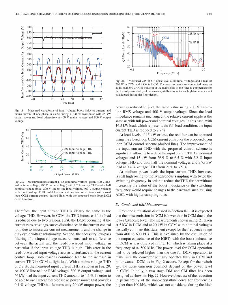
Fig. 20. Measured mains current THD at nominal voltage (green: 400 V line-to-line input voltage, 800 V output voltage) with 2.2 % voltage THD and at halfnominal voltage (blue: 200 V line-to-line input voltage, 400 V output voltage)with 0.4 % voltage THD. Solid lines indicate measurements taken with closedloop CCM current control, dashed lines with the proposed open loop DCMcurrent control.
Therefore, the input current THD is ideally the same as thevoltage THD. However, in CCM the THD increases if the loadis reduced due to two reasons. First, the DCM occurring at thecurrent zero crossings causes disturbances in the current controlloop due to inaccurate current measurements and the change induty cycle voltage relationship. Second, the necessary low-passfiltering of the input voltage measurements leads to a differencebetween the actual and the feed-forwarded input voltage, inparticular if the input voltage THD is high. This error in thefeed-forwarded input voltage acts as disturbance in the currentcontrol loop. Both reasons combined lead to the increase incurrent THD in CCM at light load. With a mains voltage THDof 2.2 %, the measured input current THD is shown in Fig. 20.At 400 V line-to-line RMS voltage, 800 V output voltage, and66 kW load the input current THD amounts to 4.5 %. In order tobe able to use a linear three-phase ac power source that provides0.4 % voltage THD but features only 20 kW output power, the
Fig. 21. Measured CISPR QP noise level at nominal voltages and a load of20 kW in CCM and 5 kW in DCM. The measurements are conducted using anadditional 390 µH CM inductor at the mains side of the filter to compensate forthe loss of permeability of the nano-crystalline inductors at high frequencies notconsidered during the filter design.
power is reduced to 14 of the rated value using 200 V line-to-
line RMS voltage and 400 V output voltage. Since the loadimpedance remains unchanged, the relative current ripple is thesame as with full power and nominal voltages. In this case, with16.5 kW load, which represents the full load condition, the inputcurrent THD is reduced to 2.7 %.
At load levels of 15 kW or less, the rectifier can be operatedusing the closed loop CCM current control or the proposed openloop DCM control scheme (dashed line). The improvement ofthe input current THD with the proposed control scheme issignificant, allowing to reduce the input current THD at nominalvoltages and 15 kW from 26.9 % to 6.5 % with 2.2 % inputvoltage THD and with half the nominal voltages and 3.75 kWload at 0.4 % voltage THD from 21% to 3.5 %.
At medium power levels the input current THD, however,is still high owing to the synchronous sampling with twice theswitching frequency. In order to reduce the THD further withoutincreasing the value of the boost inductance or the switchingfrequency would require changes to the hardware such as usingADCs with higher sampling rates.
D. Conducted EMI Measurement
From the simulations discussed in Section II-G, it is expectedthat the noise emission in DCM is lower than in CCM due to thelower CM noise level. The measurements shown in Fig. 21 takenat 5 kW in DCM and at 20 kW in CCM with nominal voltagesbasically confirms this statement except for the frequency rangefrom 400 to 600 kHz. This is explained by the oscillation ofthe output capacitance of the IGBTs with the boost inductancein DCM as it is observed in Fig. 16, which is taking place at afrequency of ≈ 500 kHz. The power level for CCM operationhad to be selected higher than the one for DCM operation tomake sure the converter actually operates fully in CCM andno unwanted DCM as in Fig. 2 occurs. Except for the switchdvdt , the noise emission does not depend on the power levelin CCM. Initially, a two stage DM and CM filter has beendesigned as shown in Fig. 22. However, because of the reductionin permeability of the nano-crystalline cores for frequencieshigher than 100 kHz, which was not considered during the filter

8810 IEEE TRANSACTIONS ON POWER ELECTRONICS, VOL. 32, NO. 11, NOVEMBER 2017
Fig. 22. Structure and component values of the two stage CM and DM EMIfilter of the prototype using a capacitive CM return path to the dc-link midpoint,damping resistors not shown. The additional CM inductor at the mains side ofthe filter is necessary to comply with CISPR Class A.
Fig. 23. Loss distribution at nominal voltages (400 V line-to-line RMS inputvoltage, 800 V output voltage) for selected operating points.
design process, an additional toroidal CM inductor of 390 µHhad to be added at the mains side of the filter to comply withCISPR Class A.
E. Loss Distribution and Efficiency
Operation of the VR with the proposed DCM scheme hastwo major effects on the losses. First, turning on the switchesat the same time leads to a higher DM voltage component atswitching frequency and thus to a higher current ripple. Thehelical windings used for the boost inductors suffer from a highac to dc resistance ratio at switching frequency, which amountsto Ra c (28 kHz)
Rd c≈ 38 according to a FEM simulation. While, this
is acceptable in CCM due to the low current ripple, the highcurrent ripple in DCM leads to a significant increase in windingloss. This effect is observed in the calculated loss distributionshown in Fig. 23 for the operating point at 13 kW, which isshown for CCM and DCM operation. On the other hand inCCM, the CM voltage component is higher. Because of the highCM inductance virtually no CM current ripple is observed, butthe higher CM voltage causes higher core losses in the CM in-ductor of the first filter stage than in DCM. The core losses inthe DM inductors are, however, higher in DCM than in CCMdue to the higher DM voltage component in DCM. Therefore, inDCM, the core losses are kind of shifted from the CM inductorof the first filter stage into the boost inductors and, according tothe calculations presented in Fig. 23, remain approximately thesame in total. The second effect on the losses in DCM concernsthe switching losses. Since the transistors are turned on at zerocurrent lower turn-on losses result compared to CCM. Since theturn-on losses are higher than the turn-off losses with the IGBTs[19] and the free-wheeling diodes [20] used, the total switching
Fig. 24. Measured efficiency in DCM and CCM compared to the calculatedvalues as function of the output power with nominal output voltage of 800 V.
Fig. 25. Thermal image of the prototype running at 10 kW in DCM withnominal voltages. The hotspot is observed at the windings of the boost inductorsnear the airgap due to the high DM current ripple. The CM inductor and theheat sink temperatures are low.
losses in DCM are lower than in CCM as shown in Fig. 23. Themeasured efficiency at nominal voltages depending on the loadis shown for CCM and DCM in Fig. 24 and compared to the cal-culated values. The calculations are based on data sheet valuesfor forward voltage drop and switching losses of the semicon-ductors, core loss data provided by the manufacturers adaptedfor the actual flux density waveform using iGSE [21] and FEMsimulations of the windings for the ac/dc resistance ratio. WithCCM the measured efficiency fits the calculated value with lessthan 0.3 % deviation at medium to high load reaching 97.2 % atfull load and a peak of 97.6 % at 24 kW. At low load the errorwith CCM control is growing, which can be explained by thepartially occurring DCM in this region not covered by the lossmodel. With the proposed open loop DCM control scheme themeasured efficiency is lower by up to 1.3 % due to the increasedcurrent ripple. Temperature measurements are carried out usinga thermal camera. The first filter stage inductors temperaturesdemonstrate the effect of high DM voltage with DCM controland high CM voltage with CCM control. With 10 kW in DCMthe thermal image is shown in Fig. 25. Due to the high currentripple the DM inductor windings heat up to 97◦C in the vicinityof the airgap, which is relatively wide with 4.5 mm. The CMinductor in this situation only heats up to 46◦C on the winding.In CCM with 32 kW output power the picture changes as shown

LEIBL et al.: SINUSOIDAL INPUT CURRENT DISCONTINUOUS CONDUCTION MODE CONTROL OF THE VIENNA RECTIFIER 8811
Fig. 26. Thermal image of the prototype running at 32 kW in CCM withnominal voltages. The hotspot is moved to the core of the CM inductance, dueto the higher CM voltage amplitude in CCM.
in Fig. 26. As expected the higher CM voltage causes the CMinductor core to heat up to 87◦C, due to the low current ripplethe temperature of the DM inductor winding drops to 61◦C eventhough the load is higher than in the situation of Fig. 25. Theheatsink temperature at 32 kW is still low with 47◦C. However,power levels higher than 40 kW could not be tested in continu-ous operation since the PCB close to the dc terminals heats upexcessively.
IV. CONCLUSION
It has been shown that an open loop DCM current controlscheme for the VR exists that allows resistive mains behavior.The expressions for the duty cycles can be derived analyticallyand are suitable for hardware implementation using look-uptables. Simulations and measurements show that a substantialreduction of input current THD is possible at light load, whichfor the prototype with ≈ 25% inductor current ripple at nomi-nal load can be considered as less than 20% of nominal load.Compared to conventional PI current control the proposed DCMcontrol scheme achieves a THD reduction from 20% to less than5%. The proposed control scheme does not rely on current mea-surements. Therefore, it is not necessary to resolve the actual lo-cal average of the inductor current in DCM. Other than commonlight load handling approaches, such as burst mode operation orincreasing the switching frequency at light load, the proposedcontrol scheme allows to operate continuously, therefore, withminimum output voltage ripple, and due to the constant switch-ing frequency the requirements for the EMI filter are not affectedif the switching frequency is less than the CISPR threshold of150 kHz. If the switching frequency is higher, 7.4 dB moreDM attenuation is required. Balancing of the output voltagesis possible with the proposed control scheme by selecting theappropriate one of two redundant switching patterns and for typ-ical modulation indices a dc current of 10% of the phase currentRMS value can be delivered to the dc-link midpoint. The highercurrent ripple of the proposed control scheme leads to higher HFwinding losses in the inductors of the first filter stage. However,zero current turn-on reduces the switching losses. The proposedcontrol scheme is implemented and verified on a 65 kW pro-totype optimized for pulse load reaching 97.2 % efficiency at
nominal load and 9.56 kW/dm3 power density using only lowcost Si components with 28 kHz switching frequency.
ACKNOWLEDGMENT
The concepts and information presented in this paper arebased on research and are not commercially available.
APPENDIX
For switching pattern A, the relative duty cycles are
D1A =D0√
y· ((9m2
min + 6mmin + 2)mmax
−(6mmin + 2)m2max − 3m3
min − 4m2min
)(18)
and
D2A = D1A · (9m2minmmax − 2m2
min −√x
− 6mminm2max + 4mmaxmmin − 3m3
min)
÷ (3m3min − 9m2
minmmax + 4m2min − 2mmax
+ 6mminm2max − 6mmaxmmin + 2m2
max) (19)
with
x = (2mmax − 2 − mmin)mmin(3mmin − 2)
·(2mmax − mmin)(m2max − m2
min) (20)
and
y = 3m5min + m4
min(7 − 15mmax)
+m3min(24m2
max − 23mmax + 2)
+m2min(20m2
max − 8mmax − 12m3max)
+mmin(√
x − 4m3max + 6m2
max)
+mmax(√
x + 2mmax − 2m2max). (21)
REFERENCES
[1] F. H. Attix, Introduction to Radiological Physics and Radiation Dosimetry.Weinheim, Germany: Wiley, 2004.
[2] H. Krieger, Strahlenphysik, Dosimetrie und Strahlenschutz - Band 2:Strahlungsquellen, Detektoren und klinische Dosimetrie. Stuttgart, Ger-many: B. G. Teubner, 1997.
[3] M. Held, P. Jacob, G. Nicoletti, P. Scacco, and M. H. Poech, “Fast powercycling test of IGBT modules in traction application,” in Proc. Int. Conf.Power Electron. Drive Syst., May 1997, vol. 1, pp. 425–430.
[4] R. Burkart and J. W. Kolar, “Overview and comparison of grid harmonicsand conducted EMI standards for LV converters connected to the MVdistribution system,” in Proc. 1st Int. Conf. Exhib. Power Electron. Intell.Motion Renew. Energy Energy Manage. Power Electron. South Amer., Sep.2012.
[5] J. W. Kolar and T. Friedli, “The essence of three-phase PFC recti-fier systems—Part I,” IEEE Trans. Power Electron., vol. 28, no. 1,pp. 176–198, Jan. 2013.
[6] J. W. Kolar and F. C. Zach, “A novel three-phase utility interface mini-mizing line current harmonics of high-power telecommunications rectifiermodules,” IEEE Trans. Ind. Electron., vol. 44, no. 4, pp. 456–467, Aug.1997.
[7] H. Uemura, F. Krismer, Y. Okuma, and J. W. Kolar, “η − ρ pareto opti-mization of three-phase three-level T-type ac-dc-ac converter comprisingSi and SiC hybrid power stage,” in Proc. Int. Power Electron. Conf., May2014, pp. 2834–2841.

8812 IEEE TRANSACTIONS ON POWER ELECTRONICS, VOL. 32, NO. 11, NOVEMBER 2017
[8] J. W. Kolar and W. Korb, “Device and method for line-voltage dependentthyristor controlled pre-charging of output capacitors in a three-level pulserectifier system,” U.S. Patent 6 377 482, Apr. 23, 2002. [Online]. Available:https://worldwide.espacenet.com/publicationDetails/biblio?FT=D&date=20020423&DB=EPODOC&locale=en_EP&CC=US&NR=6377482B1&KC=B1&ND=5
[9] M. Leibl and J. W. Kolar, “Comparative analysis of inductor concepts forhigh peak load low duty cycle operation,” in Proc. Int. Power Electron.Conf., May 2014, pp. 899–906.
[10] S. F. Lim and A. M. Khambadkone, “A simple digital DCM control schemefor boost PFC operating in both CCM and DCM,” IEEE Trans. Ind. Appl.,vol. 47, no. 4, pp. 1802–1812, Jul. 2011.
[11] P. Ide, N. Froehleke, H. Grotstollen, W. Korb, and B. Margaritis, “Anal-ysis of three-phase/three-level rectifiers at low load and discontinuousconduction mode,” in Proc. 15th IEEE Appl. Power Electron. Conf., 2000,pp. 197–204.
[12] J. W. Kolar, H. Ertl, and F. C. Zach, “Space vector-based analytical analysisof the input current distortion of a three-phase discontinuous-mode boostrectifier system,” IEEE Trans. Power Electron., vol. 10, no. 6, pp. 733–745,Nov. 1995.
[13] P. Ide, F. Schafmeister, N. Frohleke, and H. Grotstollen, “Enhanced controlscheme for three-phase three-level rectifiers at partial load,” IEEE Trans.Ind. Electron., vol. 52, no. 3, pp. 719–726, Jun. 2005.
[14] M. Leibl, J. W. Kolar, and J. Deuringer, “New current control schemefor the vienna rectifier in discontinuous conduction mode,” in Proc. IEEEEnergy Convers. Congr. Expo., Sep. 2014, pp. 1240–1247.
[15] M. Hartmann, “Ultra-compact and ultra-efficient three-phase PWM recti-fier systems for more electric aircraft,” Ph.D. dissertation, Power Electron.Syst. Lab., ETH Zurich, Zurich, Switzerland, 2011.
[16] J. W. Kolar, U. Drofenik, and F. C. Zach, “Current handling capability ofthe neutral point of a three-phase/switch/level boost-type PWM (vienna)rectifier,” in Proc. 27th IEEE Power Electron. Spec. Conf., 1996, pp. 1329–1336.
[17] M. L. Heldwein, “EMC filtering of three-phase PWM converters,” Ph.D.dissertation, Power Electron. Syst. Lab., ETH Zurich, Zurich, Switzerland,2007.
[18] International Special Committee on Radio Interference–C.I.S.P.R.,Geneva, Switzerland, “Specification for industrial, scientific and med-ical (ISM) radio-frequency equipment—electromagnetic disturbancecharacteristics—limits and methods of measurement—publication 11,”2004.
[19] Infineon Technologies AG, “IGW50N65F5—650V IGBT high speedswitching series 5th generation,” May 2015, rev. 2.1.
[20] Infineon Technologies AG, “IDW40E65D1—Emitter controlled dioderapid1 series,” Dec. 2013, rev. 2.2.
[21] K. Venkatachalam, C. R. Sullivan, T. Abdallah, and H. Tacca, “Accurateprediction of ferrite core loss with nonsinusoidal waveforms using onlysteinmetz parameters,” in Proc. IEEE Workshop Comput. Power Electron.,Jun. 2002, pp. 36–41.
Michael Leibl (M’12) received the B.Sc. degree inelectrical engineering from the Vienna University ofTechnology, Vienna, Austria, in 2010 and the M.Sc.degree in electrical engineering from the Swiss Fed-eral Institute of Technology (ETH) Zurich, Zurich,Switzerland, in 2012. He is currently working towardthe Ph.D. degree in power electronics at the PowerElectronic Systems Laboratory, ETH Zurich.
His research interests include optimized designof inductive components, in particular modeling highfrequency winding loss, high power three-phase PFC
rectifiers, and isolated dc–dc converters.
Johann W. Kolar (F’10) received the M.Sc. degree inindustrial electronics and control engineering and thePh.D. degree (summa cum laude) in electrical engi-neering both from the Vienna University of Technol-ogy, Vienna, Austria, in 1997 and 1999, respectively.
He is currently a Full Professor and the Head inthe Power Electronic Systems Laboratory, Swiss Fed-eral Institute of Technology (ETH) Zurich, Zurich,Switzerland. He has proposed numerous novel PWMconverter topologies and modulation and controlmethods (e.g., the vienna rectifier, the sparse matrix
converter, and the SWISS rectifier). His research interest include ultracom-pact and ultraefficient SiC and GaN converter systems, wireless power transfer,solid-state transformers, power supplies on chip, as well as ultrahigh speed andultralight weight drives, bearingless motors, and energy harvesting.
Dr. Kolar has supervised more than 60 Ph.D. and has published more than750 scientific papers in international journals and conference proceedings, threebook chapters, and has filed more than 140 patents. He received 25 IEEE Trans-actions and Conference Prize Paper Awards, the 2014 IEEE Power ElectronicsSociety R. David Middlebrook Achievement Award, the 2016 IEEE William E.Newell Power Electronics Award, the 2016 IEEE PEMC Council Award, andthe ETH Zurich Golden Owl Award for excellence in teaching.
Josef Deuringer received the Dipl.-Ing. (M.Sc.) de-gree in electrical engineering from the TechnicalUniversity Munich, Munich, Germany, in 1993 andthe Dr.-Ing (Ph.D.) degree in electrical engineer-ing from Friedrich-Alexander University Erlangen-Nrnberg, Erlangen, Germany, in 1998.
During his research activities he worked on highpower microwave sources for laser applications. Af-ter that, he worked for Siemens AG on numerousindustrial research and development projects for X-Ray tube beam control electronics and high-voltage
generators with high-frequency resonant inverters. He has filed 19 patents inthese areas. He is currently the Head of the Department Innovation Electronicsand Control, Siemens Healthcare GmbH, business area diagnostic imaging.