
Pulse Width Modulation of Power Electronic DC-AC Converter · Space Vector PWM 5. Artificial...
44
3 Pulse Width Modulation of Power Electronic DC-AC Converter Pulse Width Modulation (PWM) . The Pulse Width Modulation (PWM) technique is applied in the inverter (DC/AC converter) to output an AC waveform with variable voltage and variable frequency for use in mostly variable speed motor drives. . The implementation of the complex PWM algorithms have been made much easier due to the advent of fast digital signal processors, microcontrollers, and Field Programmable Gate Arrays (FPGA). Pulse Width Modulated Inverters Two Level Inverters 1. Single Phase Half Bridge Inverters 2. Single Phase Full Bridge Inverters 3. Three-phase PWM voltage source inverter Multi Level Inverters 1. Diode Clamped or Neutral point clamped multi-level inverters 2. Capacitor clamped or flying capacitor multi-level inverters 3. Cascaded H-bridge multi-level inverters Special Type Inverters 1. Impedance Source or Z-Source Inverter 2. Quasi Impedance Source or qZSI Inverter High Performance Control of AC Drives with MATLAB/Simulink Models, First Edition. Haitham Abu-Rub, Atif Iqbal, and Jaroslaw Guzinski. Ó 2012 John Wiley & Sons, Ltd. Published 2012 by John Wiley & Sons, Ltd.
Transcript of Pulse Width Modulation of Power Electronic DC-AC Converter · Space Vector PWM 5. Artificial...

3
Pulse Width Modulation of PowerElectronic DC-AC Converter
Pulse Width Modulation (PWM)
. The PulseWidthModulation (PWM) technique is applied in the inverter (DC/AC converter)
to output an AC waveform with variable voltage and variable frequency for use in mostly
variable speed motor drives.. The implementation of the complex PWMalgorithms have beenmademuch easier due to the
advent of fast digital signal processors, microcontrollers, and Field Programmable Gate
Arrays (FPGA).
Pulse Width Modulated Inverters
Two Level Inverters
1. Single Phase Half Bridge Inverters
2. Single Phase Full Bridge Inverters
3. Three-phase PWM voltage source inverter
Multi Level Inverters
1. Diode Clamped or Neutral point clamped multi-level inverters
2. Capacitor clamped or flying capacitor multi-level inverters
3. Cascaded H-bridge multi-level inverters
Special Type Inverters
1. Impedance Source or Z-Source Inverter
2. Quasi Impedance Source or qZSI Inverter
High Performance Control of AC Drives with MATLAB/Simulink Models, First Edition.Haitham Abu-Rub, Atif Iqbal, and Jaroslaw Guzinski.� 2012 John Wiley & Sons, Ltd. Published 2012 by John Wiley & Sons, Ltd.

1. Single Phase Half Bridge Inverters
The operation of the inverter can be well understood from Figure 3.2
(a) (b)
(c) (d)
Figure 3.2 Switching States in half-bridge inverter; a and c iao > 0 b and d. iao < 0.
vao
S1Da1
2dcV
vao
S’
2
V
Load AV
S1 Da22dcV
Figure 3.1 Power Circuit of a half wave bridge inverter.
2 High Performance Control of AC Drives

The output voltage is a square wave as shown in Figure 3.3
A graphical view shows that the output contains a considerable amount of low-order
harmonics such as 3rd, 5th, 7th, etc and the magnitude of the harmonics varies as the inverse of
its order.
If the modulating or control signal amplitude (Vm) > carrier signal (Vc)
The upper switch S1 is on vao ¼ Vdc
2
If the modulating or control signal amplitude (Vm) < carrier signal (Vc)
The upper switch S1’ is on vao ¼ � Vdc
2
Figure 3.4 A typical harmonic spectrum of output voltage in a half-bridge inverter.
Figure 3.3 Switching signal and the output voltage and current in a half-bridge inverter.
Pulse Width Modulation 3

The value of the average leg voltage VAO during a switching period TC can be determined
from Figure 3.6 (this shows one period of the triangular waveform).
. Matlab/Simulink Model of Half Bridge Inverter
Figure 3.6 One switching cycle in carrier-based sinusoidal PWM.
Figure 3.5 Bipolar PWM of single inverter leg.
Half-Bridge Inverter
voltage
Discrete,Ts = Ts s.
Vdc/2 = 0.5 p.u.
Vdc/2 = -0.5 p.u.
v+-
V1
Double click here to plotthe Valeg FFT
Scope2
g CE
S1'
g CE
S1
R-L Load
i+ -
I1
S1
S1'
Gate-signal Generation
Current
V inverter
I loadI load
Figure 3.7 Simulink model to implement carrier-based sinusoidal PWM.
4 High Performance Control of AC Drives

1
Out1-1double Convert1
Gain1Discrete
Edge Detector1
Data Type Conversion2 Data Type Conversion1In1
Figure 3.9b Dead band circuit.
2. Single Phase Full Bridge Inverters
Figure 3.9 Power circuit topology of a single-phase full-bridge inverter.
0.04 0.05 0.06 0.07 0.08 0.09 0.1–1
0
1
Vol
tage
[p.
u.]
Spec
trum
[p.
u.]
Time [s]
0 1000 2000 3000 4000 5000 60000
0.2
0.4
0.6
0.8 Fundamental = 0.472721
Frequency [Hz]
fc
fc-2f
mfc+2f
mfc+4f
mfc-4f
m
Figure 3.8 Output voltage and its spectrum for half bridge inverter.
Figure 3.9a Dead Band between upper and lower gating signals.
Pulse Width Modulation 5

(a) (b)
(c) (d)
Figure 3.10 Switching States in full-bridge inverter; a and c iao > 0 b and d. iao < 0.
Da1,
Db2
ON
S1,S2'
ONDa2,
Db1
ON
S2,S’1
ON
2
TT 2
3TT2
dcV
dcV−
abi,
S1, S2'
abv
S2, S1'
dcV.50
dcV.50dcV.50−
dcV.50−
aov
bov
Da1,
Db2
ON
S1,S2'
ONDa2,
Db1
ON
S2,S’1
ON
Figure 3.11 Switching signal and the output voltage and current in a half-bridge inverter.
6 High Performance Control of AC Drives

0
Vm
Vdc
0
0.5Vdc
–0.5Vdc
0
0.5Vdc
–0.5Vdc
0
VA
BV
BO
VA
O
Vdc
–Vdc
Figure 3.12 Unipolar PWM scheme for single-phase full-bridge inverter.
Pulse Width Modulation 7

. Matlab/Simulink Model of Single-phase Full-Bridge Inverter
DC/AC Full-Bridge Inverter
Discrete,Ts = 1e-005 s.
Vdc = 1 p.u.
VAB
v+-V2
Double click here to plotthe Valeg FFT
g CE
S2'
g CE
S2
g CE
S1'
g CE
S1
R-L Load
I_Load
i+ -I2
S1
S1'
S2
S2'
Gate Signal
V inverter
I load
Figure 3.13 Simulink model to implement unipolar PWM scheme in a full bridge 1-phase inverter.
0.04 0.05 0.06 0.07 0.08 0.09 0.1–2
0
2
Time [s]
0 1,000 2,000 fc 4,000 5,000 2fc 7,0000
0.2
0.4Fundamental = 0.94638
Frequency [Hz]
Spec
trum
[p.
u.]
Vol
tage
VA
B [
p.u.
]
2fc+3f
m2fc-3f
m
2fc-f
m 2fc+f
m
Figure 3.14 Voltage (VAB) and its spectrum for unipolar PWM scheme in a single-phase inverter.
8 High Performance Control of AC Drives

Three-phase PWM voltage source inverter
Figure 3.15 Power circuit topology of a three-phase voltage source inverter.
Figure 3.16 Waveforms for square wave/six-step mode of operation of a three-phase inverter.
Pulse Width Modulation 9

The maximum output phase-to-neutral voltage in the six-step mode is 0.6367 Vdc or (2/p)Vdc and that of the line to line voltage is 1.1Vdc.
vanðtÞ ¼ 2
pVDC sin vtþ 1
5sin 5vtþ 1
7sin 7vtþ 1
11sin 11vtþ 1
13sin 13vtþ . . . . . .
� �
vabðtÞ ¼ 2ffiffiffi3
p
pVDC sin vt� p
6
� �þ 1
5sin 5 vt� p
6
� �þ 1
7sin 7 vt� p
6
� �þ . . . . . .
� �
Table 3.2 Phase-to-neutral voltages for six-step mode of operation
Switching
mode
Switches ON Phase voltage
van
Phase voltage
vbn
Phase voltage
vcn
1 S1, S’2, S3 1/3Vdc � 2/3Vdc 1/3Vdc
2 S1, S’2, S’3 2/3Vdc � 1/3Vdc � 1/3Vdc
3 S1, S2, S’3, 1/3Vdc 1/3Vdc � 2/3Vdc
4 S’1, S2, S’3 � 1/3Vdc 2/3Vdc � 1/3Vdc
5 S’1, S2, S3 � 2/3Vdc 1/3Vdc 1/3Vdc
6 S’1, S’2, S3 � 1/3Vdc � 1/3Vdc 2/3Vdc
Table 3.3 Line voltages for six-step mode of operation
Switching mode Switches ON Line voltage vab Line voltage vbc Line voltage Vca
1 S1, S02, S3 Vdc �Vdc 0
2 S1, S02, S
03 Vdc 0 �Vdc
3 S1, S2, S03, 0 Vdc �Vdc
4 S01, S2, S03 �Vdc Vdc 0
5 S01, S2, S3 �Vdc 0 Vdc
6 S01, S02, S3 0 �Vdc Vdc
Table 3.1 Leg/Pole voltages of a three-phase VSI during six-step mode of operation
Switching
Mode
Switches ON Leg voltage
VA
Leg voltage
VB
Leg voltage
VC
1 S1, S’2, S3 0.5Vdc � 0.5Vdc 0.5Vdc
2 S1, S’2, S’3 0.5Vdc � 0.5Vdc � 0.5Vdc
3 S1, S2, S’3, 0.5Vdc 0.5Vdc � 0.5Vdc
4 S’1, S2, S’3 � 0.5Vdc 0.5Vdc � 0.5Vdc
5 S’1, S2, S3 � 0.5Vdc 0.5Vdc 0.5Vdc
6 S’1, S’2, S3 � 0.5Vdc � 0.5Vdc 0.5Vdc
10 High Performance Control of AC Drives

. Matlab/Simulink Model of Three-phase PWM voltage source inverter
0.04 0.05 0.06 0.07 0.08 0.09 0.1–1
0
1
Van
[p.
u.]
Spec
trum
[p.
u.]
Time [s]
0 100 200 300 400 500 600 700 800 900 10000
0.5
1Fundamental = 0.63642
Frequency [Hz]
5th 7th 11th 13th 17th 19th
Figure 3.18 Harmonic spectrum for six-step phase voltage.
DC/AC Three-phase Inverter
Discrete,Ts = 1e-005 s.
Vdc = 1 p.u.1
Vdc = 1 p.u.
Van
VAB
VA0
v+-
V4
v+-
V3
v+-
V1
Double click here to plotthe Valeg FFT
g CE
S3
g CE
S2'1
g CE
S2'
g CE
S2
g CE
S1'g C
E
S1
R-L Load1
S1
S1'
S2
S2'
S3
S3'Gate Signal
R-LLoad2
R-LLoad3
Figure 3.17 Simulink for Six-step operation of inverter.
Pulse Width Modulation 11

Pulse Width Modulation Schemes
. Classification of PulseWidthModulation Schemes for Three Phase Voltage source inverters
a. Continuous PWM
1. Carrier Based PWM Scheme
2. Third Harmonic Injection Carrier-based PWM
3. Carrier-based PWM with Offset Addition
4. Space Vector PWM
5. Artificial Neural Network Based PWM
b. Discontinuous PWM
1. Carrier based Sinusoidal PWM
VAm VBm VCm Vdc/2 V AO
Vdc/2
Van
2/3Vdc
1/3Vd
V AB
Vdc
1/3Vdc
Figure 3.18 Carrier-based sinusoidal PWM of a three-phase inverter.
12 High Performance Control of AC Drives

2
S1'
1
S1VA
>= boolean
NOT
4
S2'
3
S2VB
>= boolean
NOT
6
S3'
5
S3VC
>= boolean
NOT
Carrier Wave
Figure 3.19 Gate signal generation in Matlab for three-phase inverter.
0.04 0.05 0.06 0.07 0.08 0.09 0.1-1
0
1
Van
[p.
u.]
Time [s]
0 1,000 2,000 4000 50000
0.2
0.4Fundamental = 0.47479
Spec
trum
[p.
u.]
Frequency [Hz]fc
fc+2f
mfc-2f
m
2fc
3fc
4fc
2fc+f
m2f
c-f
m 3fc+2f
m3f
c-2f
m3f
c-2f
m 3fc+2f
m
Figure 3.20 Phase-to-neutral voltage and spectrum for carrier-based PWM.
Pulse Width Modulation 13

2. Third Harmonic Injection Carrier-based PWM
vAm ¼ Vm1sin vtð ÞþVm3sin 3vtð ÞvBm ¼ Vmsin vt� 2
p
3
� �þVm3sin 3vtð Þ
vCm ¼ Vmsin vtþ 2p
3
� �þVm3sin 3vtð Þ
Figure 3.21 Varying frequency modulation ratios for different output frequency.
Figure 3.22 Block diagram of carrier-based PWM with third-harmonic injection.
14 High Performance Control of AC Drives
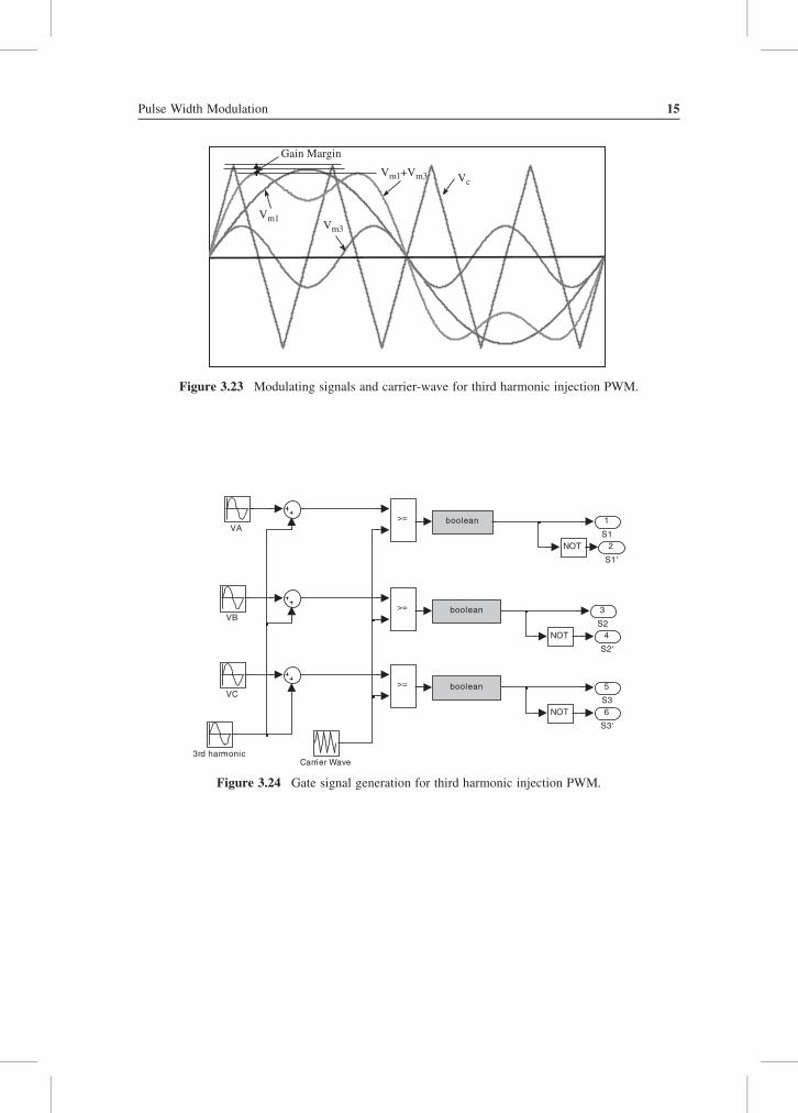
Vm1Vm3
VcVm1+Vm3
Gain Margin
Figure 3.23 Modulating signals and carrier-wave for third harmonic injection PWM.
6
S3'
5
S3
4
S2'
3
S2
2
S1'
1
S1
VC
VB
VA
>=
>=
>=
boolean
boolean
boolean
Carrier Wave
NOT
NOT
NOT
3rd harmonic
Figure 3.24 Gate signal generation for third harmonic injection PWM.
Pulse Width Modulation 15

3. Carrier-based PWM with Offset Addition
vAm ¼ Vm1 sin vtð Þþ offset
vBm ¼ Vm sin vt� 2p
3
� �þ offset
vCm ¼ Vm sin vtþ 2p
3
� �þ offset
Where offset is given as;
Offset ¼ � Vmax þVmin
2; Vmax ¼ Max vAm; vBm; vCmf g; Vmin ¼ Min vAm; vBm; vCmf g
0.04 0.05 0.06 0.07 0.08 0.09 0.1–1
0
1
Va
[p.u
.]Sp
ectr
um V
a [p
.u.]
Time [s]
0 500 1000 1500 2000 2500 3000 3500 4000 45000
0.1
0.2
Fundamental = 0.57965
Frequency [Hz]
Figure 3.25 Spectrum of phase ‘a’ voltage for third-harmonic injection.
Gain Margin Vm1
+ Offset
Vm1
Offset
Figure 3.26 Modulating signals and carrier-wave for offset addition PWM.
16 High Performance Control of AC Drives

0.04 0.05 0.06 0.07 0.08 0.09 0.1–1
0
1
Time [s]
0 500 1000 1500 2000 2500 3000 3500 4000 45000
0.1
0.2Fundamental = 0.57758
Spec
turm
Va
[p.u
.]V
a [p
.u.]
Frequency [Hz]
Figure 3.28 Output voltage and voltage spectrum for offset addition PWM.
6S3'
5S3
4S2'
3S2
2S1'
1S1
VC
VB
VA
>=
>=
>=
min
MinMax1
max
MinMax –0.5
Gain
boolean
boolean
boolean
Carrier Wave
NOT
NOT
NOT
Figure 3.27 Matlab/Simulink for offset addition PWM (File name: PWM_3_phase_CB_offset.mdl).
Pulse Width Modulation 17
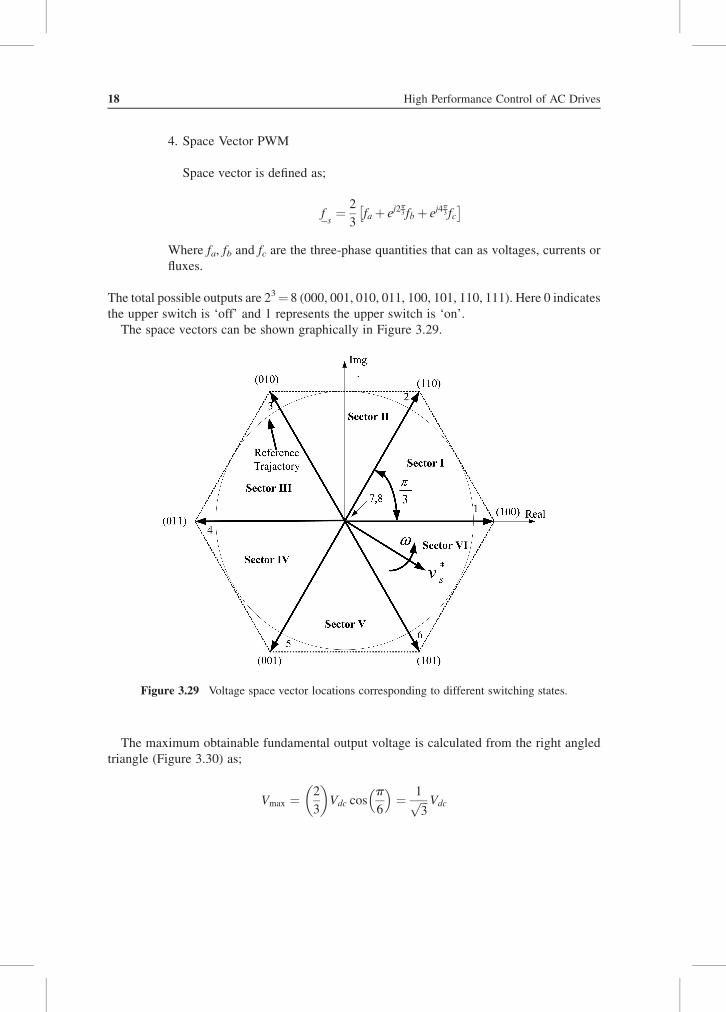
4. Space Vector PWM
Space vector is defined as;
fs¼ 2
3fa þ ej2
p3 fb þ ej4
p3 fc
� �
Where fa, fb and fc are the three-phase quantities that can as voltages, currents or
fluxes.
The total possible outputs are 23¼ 8 (000, 001, 010, 011, 100, 101, 110, 111). Here 0 indicates
the upper switch is ‘off’ and 1 represents the upper switch is ‘on’.
The space vectors can be shown graphically in Figure 3.29.
The maximum obtainable fundamental output voltage is calculated from the right angled
triangle (Figure 3.30) as;
Vmax ¼ 2
3
Vdc cos
p
6
� �¼ 1ffiffiffi
3p Vdc
Figure 3.29 Voltage space vector locations corresponding to different switching states.
18 High Performance Control of AC Drives

Discontinuous Space Vector PWM
Discontinuous space vector PWM results when one of the two zero vectors is not used in the
implementation of the space vector PWM. One of the leg of the inverter do not switch in
the whole switching period and remains tied to either the positive or negative dc bus. The nine
different discontinuous space vector PWM techniques are;
. t7¼ 0 for all sectors, known as DPWMMAX
. t8¼ 0 for all sectors, known as DPWMMIN
. Discontinuous modulation DPWM 0
. Discontinuous modulation DPWM1
. Discontinuous modulation DPWM 2
. Discontinuous modulation DPWM 3
. Discontinuous modulation DPWM 4
. Discontinuous modulation DPWM 5
. Discontinuous modulation DPWM 6
V max Vdc32
α = π/6
Figure 3.30 Determining the maximum possible output using space vector PWM.
SECTOR I
0
4/ot 2/at 2/bt 2/ot 2/bt 2/at 4/ot
ASdcV5.
dcV5.0
BS
dc.
B
SCS
7V 1V 2V 8V 2V 1V 7V2 1 7
Ts
−
Figure 3.31 Switching pattern for space vector PWM for sector I.
Pulse Width Modulation 19

V2V3 (1 1 0 )(0 1 0 )
0.4
0.6
va DPWMMAX
V1V4 (1 0 0 )t7 = 0
t7 = 0
t7 = 0
0
0.2 Vavg
V5
(0 1 1 )t7 = 0
t7 = 0
t7 = 0
-0.4
-0.2Vo
ltag
eg (
volt
s)
V NV5V6(0 0 1 ) (1 0 1 )
0.02 0.022 0.024 0.026 0.028 0.03 0.032 0.034 0.036 0.038 0.04Time (sec)
VnN
(b)(a)
DPWMMAX
Figure 3.33 (a) Zero voltage distributions (b) associated voltage waveforms for discontinuous space
vector PWM.
Figure 3.32 Leg voltage (switching pattern) for discontinuous space vector PWM.
20 High Performance Control of AC Drives

. Matlab/Simulink Model for space vector PWM:
VaSa
mag
3-Ph
VSIVbSb
Voltage
Acquisition
Low pass
Filter
reference
voltage
generator MATLAB
Function
Zero-OrderHold
VeSe
Bankangle MATLAB Fcn
RepeatingSequence
. Simulation Results for space vector PWM:
Figure 3.35 Sub-blocks of Matlab/Simulink model, a. Reference voltage generation, b. VSI, c. Filters.
Pulse Width Modulation 21

. Space Vector PWM in Over-modulation Region
Figure 3.37 a. Filtered leg voltages for continu-
ous SVPWM.
Figure 3.37 b. Filtered phase voltages for DSVPWM.
Figure 3.39 Linear and over-modulation range.
Figure 3.38 Zero vector time of application in linear modulation range in sector I.
22 High Performance Control of AC Drives

Locus of Modified Reference Vector
Desired Reference
Vector
α
*sv
*'sv
av
bv
O A
γB
C
x
y
p
q
π/3–
γFigure 3.40 Over-modulation I in space vector PWM-Case 1.
Area = A2
Area = A3
Area = A1
Locus of Modified Reference Vector
Desired Reference
Vector
α
*sv
*'sv
av
bv
AOγ
B
C
x
y
p
q
r
s
π /3
–y
Figure 3.41 Over-modulation I in SVPWM-Case 2.
Pulse Width Modulation 23

. Matlab/Simulink Model to implement space vector PWM in Over-modulation Regions
. Harmonic Analysis
Harmonic component of the output voltage is given using the Fourier series expression as:
FnðuÞ ¼ 4
p
ðp=20
f ðuÞsinðnuÞdu
264
375
0
0.2
0.4
0.6
0
0.2
0.4
0.6
0.02 0.03 0.04 0.05 0.06 0.07 0.08 0.09 0.1
-0.6
-0.4
-0.2
volta
ge(v
olts
)
0.02 0.03 0.04 0.05 0.06 0.07 0.08 0.09 0.1
-0.6
-0.4
-0.2
volt
age(
volt
s)
time (sec)time(sec)
0.6
0.4
0.6
(b) MI = 0.952(a) MI = 0.907
-0.2
0
0.2
0.4
volt
age(
volt
s)
-0.2
0
0.2
volt
age(
volt
s)
0.02 0.03 0.04 0.05 0.06 0.07 0.08 0.09 0.1
-0.6
-0.4
time (sec)0.02 0.03 0.04 0.05 0.06 0.07 0.08 0.09 0.1
-0.6
-0.4
time(sec)
(d) MI = 1.000(c) MI = 0.980
Figure 3.43 Inverter Phase ‘a’ voltage waveform at different modulation indices.
Locus of Modified Reference Vector
Desired Reference
Vector
α
*sv
*'sv
Oγ x
y
pq
mα
π/3
–y
Figure 3.42 Over-modulation II in space vector PWM.
24 High Performance Control of AC Drives

. Total Harmonic Distortion (THD)
The Total Harmonic Distortion (THD) factor is defined as
THD ¼ffiffiffiffiffiffiffiffiffiffiffiffiffiffiffiffiffiffiffiffiffiV2r �V2
1
� �qV21
Total Harmonic Distortion
35
20
25
30
10
15TH
D [
%]
0
5
10.990.980.970.960.950.940.930.920.910.9
MI
Figure 3.45 Total Harmonic Distortion in over-modulation region.
Figure 3.44 Harmonic spectra by FFT, normalized to fundamental component.
Pulse Width Modulation 25

5. Artificial Neural Network Based PWM
0 0.004 0.01 0.016 0.02–1.5
–1
–0.5
g A(α
*), g
B(α
*), g
C(α
*)
0
0.5
1
1.5
Time (s)
Figure 3.47 Turn –on pulse width function of phase A, B, C as a function of Angle a in different sector.
Norm
alization
De-no
rmalization
V*
α* Ts/4
UP/Down
Counter
Sa
Sb
Sc
( )*Vf
( )*αg
Neural Network
Figure 3.46 Functional Block diagram of ANN based Space Vector PWM for a three-phase VSI.
26 High Performance Control of AC Drives

. Matlab/Simulink Model of Implementing ANN based Space Vector PWM
3Sc
2Sb
1Sa
comparatorblock
Subsystem1
RepeatingSequence
Product2
Product1
Product
x{1}
g{a}
g{b}
g{c}
Neural Network
-K-
Gain
T/4
Constant1
Cartesian toPolar
2Vq
1Vd
3
g{c}
2
g{b}
1
g{a}a{3}
a{2}
a{1}
ya
Process Output 1
px
Process Input 1
a{4}a{3}
Layer 4
a{3}a{2}
Layer 3
a{2}a{1}
Layer 2
a{1}p{1}
Layer 1
a{3}
a{2}
a{1}
1
x{1}
Figure 3.48 Matlab/Simulink model of ANN based space vector PWM.
0.02 0.022 0.024 0.026 0.028 0.03 0.032 0.034 0.036 0.038 0.04–1
0
1
0.02 0.022 0.024 0.026 0.028 0.03 0.032 0.034 0.036 0.038 0.040
0.5
1
0.02 0.022 0.024 0.026 0.028 0.03 0.032 0.034 0.036 0.038 0.04–1
0
1
Time (s)
VA
-fil
tere
d (p
.u.)
Leg
vol
tage
(p.
u.)
VA
(p.
u.)
Figure 3.49 ANN based Space vector PWM waveforms.
Pulse Width Modulation 27

Table 3.5 Relationship between the space vector and modulating signal
Sector No. UA UB UC
I ðta þ tb þ t8 þ t7Þ=Ts ð� ta þ tb þ t8 � t7Þ=Ts ð� ta � tb þ t8 � t7Þ=TsII ðta � tb þ t8 � t7Þ=Ts ðta þ tb þ t8 � t7Þ=Ts ð� ta � tb þ t8 � t7Þ=TsIII ð� ta � tb þ t8 � t7Þ=Ts ðta þ tb þ t8 � t7Þ=Ts ð� ta þ tb þ t8 � t7Þ=TsIV ð� ta � tb þ t8 � t7Þ=Ts ðta � tb þ t8 � t7Þ=Ts ðta þ tb þ t8 � t7Þ=TsV ð� ta þ tb þ t8 � t7Þ=Ts ð� ta � tb þ t8 � t7Þ=Ts ðta þ tb þ t8 � t7Þ=TsIV ðta þ tb þ t8 � t7Þ=Ts ð� ta � tb þ t8 � t7Þ=Ts ðta � tb þ t8 � t7Þ=Ts
Figure 3.50 Relationship between carrier-based and space vector PWM in sector I.
Figure 3.51 Relationship between modulating signal and space vector sectors.
28 High Performance Control of AC Drives

Multi-level Inverters
The most popular configurations are;
1. Diode Clamped or Neutral point clamped multi-level inverters
2. Capacitor clamped or flying capacitor multi-level inverters
3. Cascaded H-bridge multi-level inverters
1. Diode Clamped Multi-level Inverters
The leg voltages can then be written as
VAN ¼ SA1 � SA2ð ÞVdc
VBN ¼ SB1 � SB2ð ÞVdc
VCN ¼ SC1 � SC2ð ÞVdc
Figure 3.52 Neutral Point Clamped 3-level inverter topology.
Pulse Width Modulation 29

Time [s](a)
Car
rier
and
Mod
ulat
ing
wav
e [p
.u.]
Car
rier
and
Mod
ulat
ing
wav
e [p
.u]
Car
rier
and
Mod
ulat
ing
wav
e [p
.u.]
0 Time [s](b)
Time [s](c)
Figure 3.53 Principle of SPWM for a five-level diode clamped inverter: (a) IPD; (b) POD;
and (c) APOD.
30 High Performance Control of AC Drives

. Matlab/Simulink Model of Carrier-based PWM scheme for three-level NPC
1
dc
ia
ib
ic
Sa
Sb
Sc
Vdc
Vc1
Vc2
Double click here to plotthe Valeg FFT
Sa
Sb
Sc
S-PWM
van
vbn
vcn
ia
ib
ic
R-L Load
Vc1
Vc2
Sabc
Van
Vbn
Vcn
Figure 3.54 Matlab/Simulink model of Carrier-based PWM for a 3-level NPC.
–1
–1.5
–0.5
0
0.5
Phas
e 'a
' vol
tage
[p.
u.]
Lin
e vo
ltage
Vab
[p.
u.]
Phas
e 'a
' vol
tage
[p.
u.]
Spec
trum
vol
tage
[p.
u.]
Phas
e cu
rren
ts [
p.u.
]
1
1.5
0 0.005 0.01 0.015 0.02 0.025 0.03 0.035 0.04
–2
–1
0
1
1.5
0.5
–0.5
–1.5
–2.5
2
2.5
Time [s]
0 0.005 0.01 0.015 0.02 0.025 0.03 0.035 0.04–0.06
–0.04
–0.02
0
0.02
0.04
0.06
Time [s]
0 0.005 0.01 0.015 0.02 0.025 0.03 0.035 0.04–2
0
2
Time [s]
0 1000 2000 3000 4000 5000 6000 7000 80000
0.05
0.1Fundamental = 0.89287
Frequency [Hz]
0 0.005 0.01 0.015 0.02 0.025 0.03 0.035 0.04Time [s]
Figure 3.55 Response of a three-level NPC.
Pulse Width Modulation 31

2. Flying Capacitor Type Multi-level Inverter
Figure 3.56 Power Circuit of a 3-level three-phase flying capacitor type inverter.
32 High Performance Control of AC Drives

0.5V
dc
C
va
Sa1
Sa1
Da1
Da1
Da2
Da2
Da3
Da3
Da4
Da4
Da1
Da2
Da3
Da4
Da1
Da2
Da3
Da4
Da1
Da2
Da3
Da4
Da1
Da2
Da3
Da4
Da1
Da2
Da3
Da4
Sa2
Sa2
S’a2
S’a2
Sa1
Sa2
S’a2
S’a1S’a1
S’a1
Sa1
Sa2
S’a2
S’a1
Sa1
Sa2
S’a2
S’a1
Sa1
Sa2
S’a2
S’a1
Sa1
Sa2
S’a2
S’a1
Sa1
Sa2
S’a2
S’a1
Cf
(a)va
Cf
Da1
Da2
Da3
Da4
C1
C2
(b)
0.5V
dc
0.5V
dc0.
5Vdc
va
Cf
0.5V
dc0.
5Vdc
C1
C2
(c)va
Cf
0.5V
dc0.
5Vdc
C1
C2
(d)
va
Cf
0.5V
dc0.
5Vdc
C1
C2
(e)va
Cf
0.5V
dc0.
5Vdc
C1
C2
(f)
va
Cf
0.5V
dc0.
5Vdc
C1
C2
(g) va
Cf
0.5V
dc0.
5Vdc
C1
C2
(h)
Figure 3.57 (a) Switch State 1100with positive current flow; (b) Switch state 1100with negative current
flow; (c) Switch state 1010 with positive current flow (Flying capacitor charges); (d) Switch state 1010
with negative current flow (Flying capacitor discharges); (e) Switch state 0101 with positive current flow
(Flying capacitor discharges); (f) Switch state 0101with negative current flow (Flying capacitor charges);
(g) Switch state 0011 with positive current flow; (h) Switch state 0011 with negative current flow.
Pulse Width Modulation 33

Vdc
0Ts 2Ts 3Ts 4Ts
Vdc/2
Vdc/2
Figure 3.59 Carrier wave for Sn2 and Sn20 in FLC inverter.
Vdc /2
Ts 2Ts 3Ts 4Ts
0
Sn1
Sn2
Figure 3.61 Gate signal generation when 0 � vref � Vdc=2.
Vdc
Ts 2Ts 3Ts 4Ts
Vdc /2
S n1
Sn2
Figure 3.60 Gate signal generation when Vdc=2 � vref � Vdc.
Vdc
0Ts 2Ts 3Ts 4Ts
Vdc/2
Vdc/2
Figure 3.58 Carrier wave for Sn1 and Sn10 in FLC inverter.
34 High Performance Control of AC Drives

.Matlab/SimulinkModel
of3-level
CapacitorClamped
orFLCinverter
Dis
cre
te,
Ts
= 1
e-0
05
s.
po
we
rgu
i
v+ -
Vo
ltage
Me
asu
rem
ent
4
v+ -
Vo
ltage
Me
asu
rem
ent
1
Sco
pe
5S
cop
e3
Sco
pe
2
C5
Vo
ltage
Me
asu
rem
ent
4
v+ -
Vol
tage
Me
asu
rem
ent
2
g
CE
Sa
5
g
CE
Sa
3
g
CE
Sa
1
C7
C6
C1
Vdc
g
CE
Sa
6
g
CE
Sa
4
g
CE
Sa
2
C4
C3
C1
Sco
pe
1
g
C
g
C
g
C
g
CE
Sa
1'2
g
CE
Sa
1'1
g
CE
Sa
1'i
+-
Cur
rent
Me
asu
rem
ent
Out
1
Out
2O
ut1
Out
2
Out
1
Out
2
v+ -
Vol
tage
Me
asu
rem
ent
5S
cop
e6
E
Sa
2'2
E
Sa
2'1
E
Sa
2'
Out
3
Out
4
swu
tch
sta
te2
Out
2
Out
3
Out
4
swu
tch
sta
te1
Out
2
Out
3
Out
4
swu
tch
sta
te
Pulse Width Modulation 35

3. Cascaded H-Bridge Multi-level Inverter
va vb vc
Sa11 Sa22 Sb11 Sb22 Sc11 Sc22
S’a11 S’
a22
dcV
S’b11 S’
b22
dcV
S’c11 S’
c22
dcV1Nv
Sa12 Sa21
dcV
Sb12 Sb21
dcV
Sc12 Sc21
dcV2Nv
S’a12 S’
a21 S’b12 S’
b21 S’c12 S’
c21
Figure 3.64 Power circuit topology of a five-level Cascaded H-bridge inverter.
0 0.01 0.02 0.03 0.04 0.05 0.06 0.07 0.08 0.09 0.1–1000
0
1000
Vab
(V)
Van
(V)
0 0.01 0.02 0.03 0.04 0.05 0.06 0.07 0.08 0.09 0.1
–500
0
500
Time [s]
Figure 3.63 Output line and phase voltages from 3-level FLC inverter.
36 High Performance Control of AC Drives

.Matlab/SimulinkModel
of5-level
CHBinverter
OU
PU
T-1
O
UT
PU
T -
3
OU
TP
UT
-2
Con
tinuo
us
pow
ergu
i
Vdc
8
Vdc
7
Vdc
5
Vdc
4
Vdc
2
Vdc
1
v+ - V
8
v+ - V
7
v+ - V
3
v+ -
V1
Sco
pe3
Sco
pe1
Sco
pe
In2
Out
1
Out
2
INV
ER
TE
R P
WM
LO
GIC
2
In2
Out
1
Out
2
INV
ER
TE
R P
WM
LO
GIC
1
In2
Out
1
Out
2
INV
ER
TE
R P
WM
LO
GIC
gC
E
IGB
T2_
9
gC
E
IGB
T2_
8
gC
E
IGB
T2_
7
gC
E
IGB
T2_
3
gC
E
IGB
T2_
27
gC
E
IGB
T2_
26
gC
E
IGB
T2_
25
gC
E
IGB
T2_
21
gC
E
IGB
T2_
20g
C
E
IGB
T2_
2
gC
E
IGB
T2_
19
gC
E
IGB
T2_
18
gC
E
IGB
T2_
17
gC
E
IGB
T2_
16
gC
E
IGB
T2_
12
gC
E
IGB
T2_
11
gC
E
IGB
T2_
10g
C
E
IGB
T2_
1
gC
E
IGB
T1_
9
gC
E
IGB
T1_
7
gC
E
IGB
T1_
6
gC
E
IGB
T1_
4
gC
E
IGB
T1_
3
gC
E
IGB
T1_
1
[aaG
1_2]
[aG
1_2]
-T-
[aG
1_2A
]
[aG
4_2A
]
[aG
4_2]
[aG
3_2A
]
-T-
-T-
-T-
[aG
2_2A
]
-T-
[aG
3_2]
[aG
1_2K
]
[aG
4_2K
]
[aG
3_2K
]
-T-
-T-
-T-
[aG
2_2K
]
[aaG
4_2]
[aaG
3_2]
[aaG
2_2]
[aG
2_2]
-T-
[aG
1_2]
-T-
-T-
-T-
[aG
4_2]
-T--T
--T-
-T-
-T-
-T-
[aG
3_2]
-T-
-T--T-
-T--T-
-T-
-T-
-T--T-
-T-
[aG
2_2]
0.9
Con
stan
t
1 oh
31
oh2
1 oh
1
Figure
3.65
Matlab/Sim
ulinkof5-level
3-phaseCHB.
Pulse Width Modulation 37

1. Impedance Source or Z-Source Inverter
Circuit Analysis
Figure 3.68 Equivalent circuit of a Z-source inverter; (a). non-shoot-through mode, (b). shoot through
mode.
0.01 0.02 0.03 0.04 0.05 0.06 0.07 0.08 0.09 0.1–5
0
5
0 0.01 0.02 0.03 0.04 0.05 0.06 0.07 0.08 0.09 0.1–2
0
Vab
( p.
u)V
ab(
p.u)
2
Time [s]
Figure 3.66 Output line and phase voltages from 5-level CHB inverter.
Figure 3.67 Power circuit topology of a Z-source inverter.
38 High Performance Control of AC Drives

. Carrier-based Simple Boost PWM control of a Z-source Inverter
. Carrier-based Maximum Boost PWM control of a Z-source Inverter
v*a
v*b
v*c
V*N
V*P
S1
S2
S3
S’3S’2S’1
1
1
1
1
1
0
1
0
0
0
0
0
1
0
0
1
1
0
1
1
1
0
0
0
Carrier Modulating signals
Shoot-through zero states
Figure 3.69 Principle of Carrier-based simple boost PWM for a Z-source inverter.
0 0.80.60.40.2
10
4
2
Modulation Index (M)
Vol
tage
Gai
n (G
)
10
8
6
Maximum constant boost
Simple boost
Figure 3.71 Voltage gain versus modulation index for Z-source inverter.
v*a
v*b
v*c
V*N
V*P
S1
S2
S3
S’3S’2
S’1
1
1
0
1
0
0
1
0
0
1
1
0
CarrierModulating signals
Shoot-through zero states
1
1
1
0
0
0
0
0
0
1
1
1
Figure 3.70 Principle of Carrier-based Maximum boost PWM for a Z-source inverter.
Pulse Width Modulation 39

.Matlab/Sim
ulinkmodel
ofZ-sourceinverter
ZS
I
Dis
cre
te,
Ts
= 1
e-0
06
s.
ZS
IO
UT
PU
T
VA
RIA
BL
E L
OA
D
Iso
late
d L
oa
d
INP
UT
Va
b
Vc1
Vc2
Iab
c
Va
bc
Iin
Vin
D
Va
b_
filt
ere
dV
pn
DC
-so
urc
e
ZS
I C
AR
RIE
R B
AS
ED
CO
NT
RO
L
Co
mm
an
de
d V
olt
ag
e
Figure
3.72
Matlab/Sim
ulinkmodel
ofZ-sourceinverter(Filenam
e:ZSI_SPWM_RL_load.mdl).
40 High Performance Control of AC Drives

0 0.1 0.2 0.3 0.4 0.5 0.6 0.7 0.8 0.9 1-200
0
200
Vab
c Filt
ered
(V
)
0 0.1 0.2 0.3 0.4 0.5 0.6 0.7 0.8 0.9 1-20
0
20
I abc (
A)
0 0.1 0.2 0.3 0.4 0.5 0.6 0.7 0.8 0.9 1-1000
0
1000
Vab
(V
)
Figure 3.74 Outputs from Z-Source inverter, a. Filtered three-phase voltages, b. Three-phase load
current, c. Line voltage.
0 0.1 0.2 0.3 0.4 0.5 0.6 0.7 0.8 0.9 1–1000
0
1000
Vin
v (V
)V
c1 a
nd V
c2 (
V)
VL
1 an
d V
L2
(V)
0 0.1 0.2 0.3 0.4 0.5 0.6 0.7 0.8 0.9 10
500
0 0.1 0.2 0.3 0.4 0.5 0.6 0.7 0.8 0.9 1–500
0
500
Time (s)
Figure 3.73 Voltages at the source side, a. at the input of the bridge inverter, b. across two capacitors, c.
across two inductors.
Pulse Width Modulation 41

2. Quasi Impedance Source or qZSI Inverter
Circuit Analysis
Figure 3.76 Equivalent circuit of the qZSI; (a) non-shoot-through state, (b) shoot-through state.
Impedance Network, qZSI
2cv
S SS
DC Source
L1 C2
1Li 2Li
1Lv
L2
2Lv
VCVB
S2 S3 Dc1Db2
VA
S1Da1
2dcV
o C1 1cv invv
S’2 S’
3Db2 Dc2S’
1 Da22dcV
Figure 3.75 Power Circuit topology of the voltage fed qZSI.
42 High Performance Control of AC Drives

.Matlab/Simulinkmodel
ofqZ-sourceinverter
QZ
SI
Disc
rete
,Ts
= 1
e-00
6 s.
Vab
1
OU
TP
UT
VA
RIA
BL
E L
OA
D
Isol
ated
Loa
d
INP
UT
Va
b
Vc1
Vc2
Iab
c
Va
bc
Iin
Vin
DV
ab_f
ilter
ed
Vp
n
Fo20
H
DC
-sou
rceQZS
I CAR
RIE
R B
ASED
CO
NTR
OL
Con
trol
Co
mm
an
de
dV
olt
ag
e
Figure
3.77
Matlab/Sim
ulinkmodel
ofZ-sourceinverter.
Pulse Width Modulation 43

0 0.1 0.2 0.3 0.4 0.5 0.6 0.7 0.8 0.9 1-200
0
200
Vab
c Filt
ered
(V
)
0 0.1 0.2 0.3 0.4 0.5 0.6 0.7 0.8 0.9 1-20
0
20
I abc (
A)
0 0.1 0.2 0.3 0.4 0.5 0.6 0.7 0.8 0.9 1-1000
0
1000
Time (s)
Vab
(V
)
Figure 3.79 Outputs from qZ-Source inverter, a. Filtered three-phase voltages, b. Three-phase load
current, c. Line voltage.
0 0.1 0.2 0.3 0.4 0.5 0.6 0.7 0.8 0.9 1-1000
0
1000
Vin
v (V
)
0 0.1 0.2 0.3 0.4 0.5 0.6 0.7 0.8 0.9 10
200
400
Vc1
and
Vc2
(V
)
0 0.1 0.2 0.3 0.4 0.5 0.6 0.7 0.8 0.9 1-500
0
500
Time (s)
VL
1 and
VL
2 (V
)
Figure 3.78 Voltages at the source side: upper - at the input of the bridge inverter; middle - across two
capacitors; lower - across two inductors.
44 High Performance Control of AC Drives