(LDO Papers Useful) ASICON 20 2009 8th IEEE International Conference on ASIC
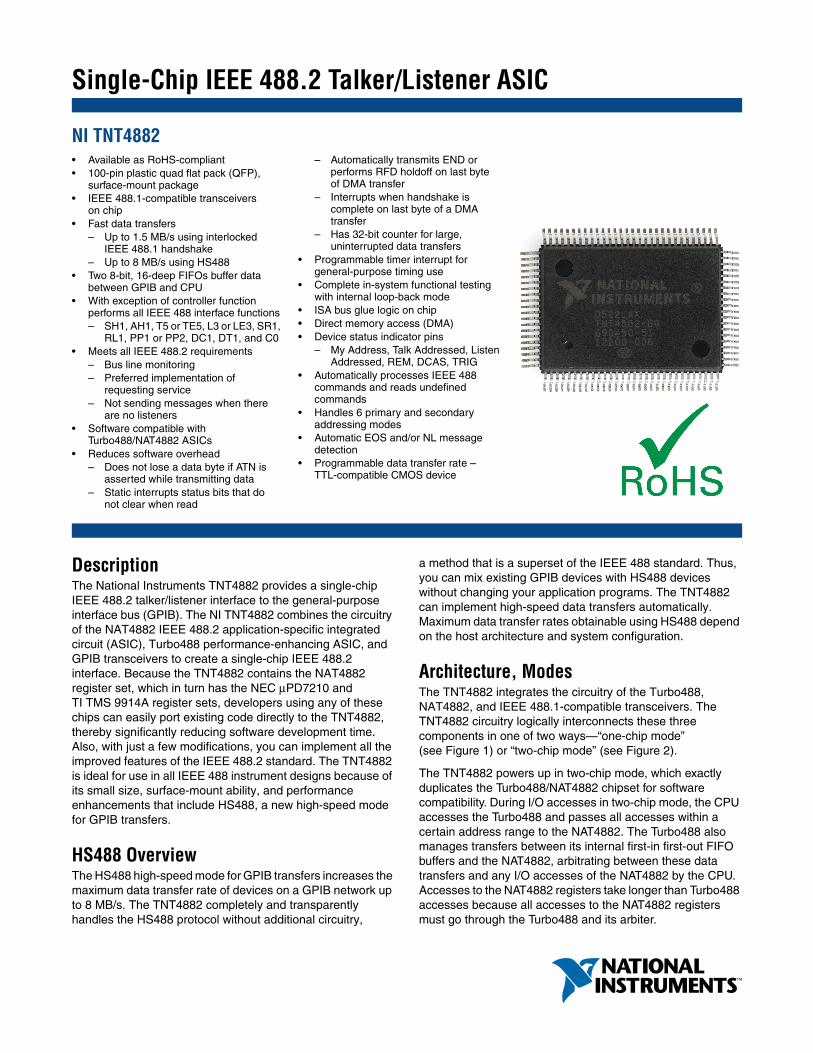
Single-Chip IEEE 488.2 Talker/Listener ASIC
NI TNT4882
DescriptionThe National Instruments TNT4882 provides a single-chip IEEE 488.2 talker/listener interface to the general-purpose interface bus (GPIB). The NI TNT4882 combines the circuitry of the NAT4882 IEEE 488.2 application-specific integrated circuit (ASIC), Turbo488 performance-enhancing ASIC, and GPIB transceivers to create a single-chip IEEE 488.2 interface. Because the TNT4882 contains the NAT4882 register set, which in turn has the NEC μPD7210 and TI TMS 9914A register sets, developers using any of these chips can easily port existing code directly to the TNT4882, thereby significantly reducing software development time. Also, with just a few modifications, you can implement all the improved features of the IEEE 488.2 standard. The TNT4882 is ideal for use in all IEEE 488 instrument designs because of its small size, surface-mount ability, and performance enhancements that include HS488, a new high-speed mode for GPIB transfers.
HS488 OverviewThe HS488 high-speed mode for GPIB transfers increases the maximum data transfer rate of devices on a GPIB network up to 8 MB/s. The TNT4882 completely and transparently handles the HS488 protocol without additional circuitry,
a method that is a superset of the IEEE 488 standard. Thus, you can mix existing GPIB devices with HS488 devices without changing your application programs. The TNT4882 can implement high-speed data transfers automatically. Maximum data transfer rates obtainable using HS488 depend on the host architecture and system configuration.
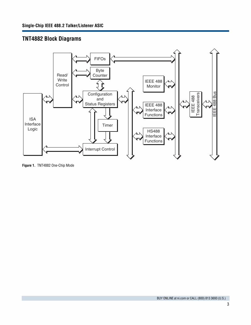
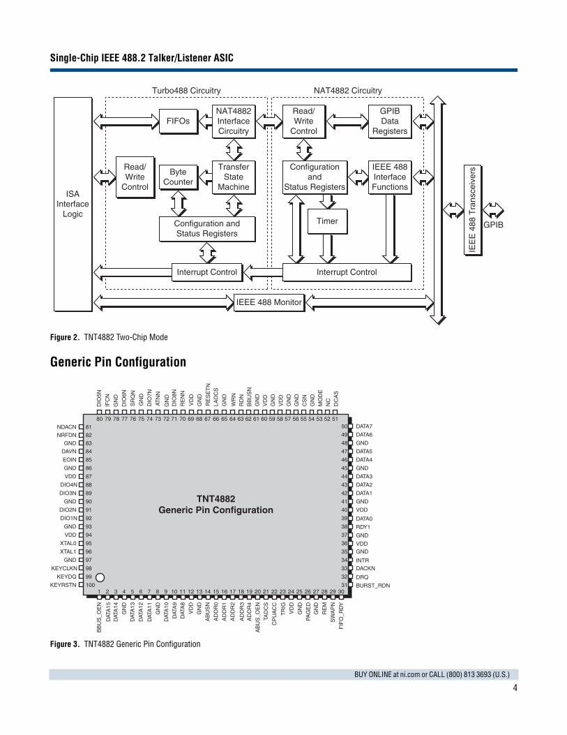
Architecture, ModesThe TNT4882 integrates the circuitry of the Turbo488, NAT4882, and IEEE 488.1-compatible transceivers. The TNT4882 circuitry logically interconnects these three components in one of two ways—“one-chip mode” (see Figure 1) or “two-chip mode” (see Figure 2).
The TNT4882 powers up in two-chip mode, which exactly duplicates the Turbo488/NAT4882 chipset for software compatibility. During I/O accesses in two-chip mode, the CPU accesses the Turbo488 and passes all accesses within a certain address range to the NAT4882. The Turbo488 also manages transfers between its internal first-in first-out FIFO buffers and the NAT4882, arbitrating between these data transfers and any I/O accesses of the NAT4882 by the CPU. Accesses to the NAT4882 registers take longer than Turbo488 accesses because all accesses to the NAT4882 registers must go through the Turbo488 and its arbiter.
• Available as RoHS-compliant• 100-pin plastic quad flat pack (QFP),
surface-mount package • IEEE 488.1-compatible transceivers
on chip • Fast data transfers
– Up to 1.5 MB/s using interlocked IEEE 488.1 handshake
– Up to 8 MB/s using HS488 • Two 8-bit, 16-deep FIFOs buffer data
between GPIB and CPU• With exception of controller function
performs all IEEE 488 interface functions – SH1, AH1, T5 or TE5, L3 or LE3, SR1,
RL1, PP1 or PP2, DC1, DT1, and C0 • Meets all IEEE 488.2 requirements
– Bus line monitoring – Preferred implementation of
requesting service– Not sending messages when there
are no listeners• Software compatible with
Turbo488/NAT4882 ASICs • Reduces software overhead
– Does not lose a data byte if ATN is asserted while transmitting data
– Static interrupts status bits that do not clear when read
– Automatically transmits END or performs RFD holdoff on last byte of DMA transfer
– Interrupts when handshake is complete on last byte of a DMA transfer
– Has 32-bit counter for large, uninterrupted data transfers
• Programmable timer interrupt for general-purpose timing use
• Complete in-system functional testing with internal loop-back mode
• ISA bus glue logic on chip • Direct memory access (DMA) • Device status indicator pins
– My Address, Talk Addressed, Listen Addressed, REM, DCAS, TRIG
• Automatically processes IEEE 488 commands and reads undefined commands
• Handles 6 primary and secondary addressing modes
• Automatic EOS and/or NL message detection
• Programmable data transfer rate – TTL-compatible CMOS device
Single-Chip IEEE 488.2 Talker/Listener ASIC
2BUY ONLINE at ni.com or CALL (800) 813 3693 (U.S.)
To achieve higher data transfer rates, you can switch the TNT4882 to one-chip mode in software. In one-chip mode, the FIFO buffer connects directly to the GPIB transceivers and the CPU accesses all registers directly. You can access NAT4882 registers in the same amount of time as Turbo488 registers because accesses to these registers do not go through the Turbo488.
The NAT4882 portion of the TNT4882 can emulate either the NEC μPD7210 or the TI TMS9914A GPIB controller chips. The state of one of the TNT4882 input pins determines the chip emulation mode on power up, but you can switch the chip emulation mode back and forth between 7210 and 9914 modes through software.
The register map of the NAT4882 portion of the TNT4882 changes to emulate either the 7210 or the 9914, but the Turbo488 registers are identical in both chip emulation modes. You cannot use one-chip mode with the 9914 emulation mode. Because the Turbo488 was designed to interface to the 7210 and not the 9914, the software can rearrange the register map of the 9914 mode NAT4882 registers so that the 9914 mode Command/Data Out Register and Data In Register and the Auxiliary Command Register appear at the same addresses as the corresponding 7210 mode registers. The Turbo488 can then perform DMA transfers with the NAT4882 in 9914 mode.
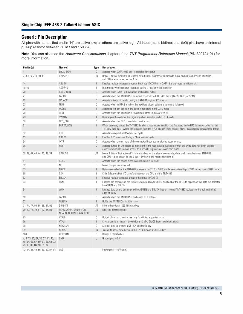
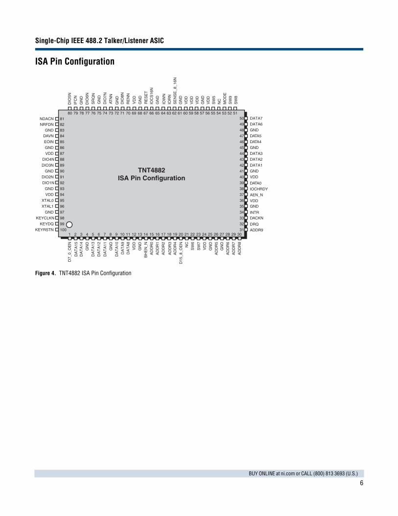
The TNT4882 has two different pin configurations – Generic (see Figure 3) and ISA (see Figure 4). The TNT4882 determines which configuration to use by the location of the power (VDD) and ground pins. The Generic pin configuration provides a simple interface to any CPU. Using the ISA pin configuration, you can connect the TNT4882 directly to an ISA (IBM PC AT) bus without any external glue logic or data transceivers. You can also use the ISA pin configuration TNT4882 with an 8-bit (PC/XT) bus. You may want to use the ISA version for interfaces other than an ISA bus to take advantage of the built-in 5-bit address decoder. You can use two-chip mode, one-chip mode, 7210 mode, and 9914 mode identically with either pin configuration.
RoHS ComplianceThe TNT4882 is currently available from NI both in a standard package and as a RoHS-compliant chip. The chips can be ordered using the part numbers shown in the Ordering Information box below. The RoHS-compliant parts are identified through the added “F” at the end of the part number and the chip itself is marked with an e3 inside an ellipse to indicate a matte pure tin finish on the leads, in accordance with the marking recommendations defined in JEDEC JESD97.
The RoHS-compliant TNT4882 meets industry requirements for baking and maximum solder reflow temperature. The baking requirements are outlined in JEDEC J-STD-033, and NI recommends using the solder reflow profile as shown in IPC/JEDEC J-STD-020C with a peak temperature of 260 °C, the maximum temperature they can withstand. The Moisture Sensitivity Level (MSL) for the RoHS-compliant surface mount TNT4882 ASIC is 3.
Ordering Information
NI TNT4882-BQ (100-pin QFP package)
RoHS-compliant..............................................TNT4882-BQF66
Non RoHS-compliant ........................................ TNT4882-BQ66
Developer kit (RoHS-compliant................................. 776866-01
Sample kit (RoHS-compliant, 5 ASICs) .................... 778609-01
Visit ni.com for a detailed reference manual & specifications.
BUY NOW!For complete product specifications, pricing, and accessory information, call (800) 813 3693 (U.S.) or go to ni.com/gpib.
Single-Chip IEEE 488.2 Talker/Listener ASIC
3BUY ONLINE at ni.com or CALL (800) 813 3693 (U.S.)
TNT4882 Block Diagrams
Figure 1. TNT4882 One-Chip Mode
FIFOs
ByteCounter
Configurationand
Status Registers
Interrupt Control
Timer
Read/Write
Control
ISAInterface
Logic
IEEE 488InterfaceFunctions
HS488InterfaceFunctions
IEEE 488Monitor
IEE
E 4
88T
rans
ceiv
ers
IEE
E 4
88 B
us
Single-Chip IEEE 488.2 Talker/Listener ASIC
4BUY ONLINE at ni.com or CALL (800) 813 3693 (U.S.)
Figure 2. TNT4882 Two-Chip Mode
Generic Pin Configuration
Figure 3. TNT4882 Generic Pin Configuration
Interrupt Control
ISAInterface
Logic
NAT4882InterfaceCircuitry
ByteCounter
TransferState
Machine
Configuration andStatus Registers
IEEE 488InterfaceFunctions
GPIBData
Registers
Configurationand
Status Registers
Timer
Read/Write
Control
FIFOs
Interrupt Control
Read/Write
Control
IEEE 488 Monitor
Turbo488 Circuitry NAT4882 Circuitry
IEE
E 4
88 T
rans
ceiv
ers
GPIB
DIO
6N
GN
D
LAD
CS
DIO
8N
GN
D
IFC
N
DIO
5N
SR
QN
GN
D
DIO
7N
ATN
N
RE
NN
GN
D
RE
SE
TN
80 79 78 77 76 75 74 73 72
84
85
86
87
88
89
90
91
92
93
94
95
96
97
98
99
1001 2 3 4 5 6 7 8 9 10 11 12 13 14 15 16 17
71 70 69 68 67 66 65 64
31
32
33
34
35
36
37
38
39
40
41
42
43
44
45
46
47
GN
D
DATA5
DATA4
GND
GND
VDDGND
DATA0
INTRDACKN
DRQ
BURST_RDN
DAVN
GND
VDD
GND
DIO2N
DIO1N
DIO3N
VDD
XTAL1
EOIN
WR
N
GN
D
VD
D
TR
IG
CP
UA
CC
TAD
CS
AB
US
_OE
N
AD
DR
4A
DD
R3
AD
DR
2
AD
DR
1
AD
DR
0
AB
US
N
PAG
ED
GN
D
RE
M
SW
AP
N
FIF
O_R
DY
TNT4882Generic Pin Configuration
DIO4N
GND
XTAL0
GND
KEYCLKN
KEYDQ
KEYRSTN
DATA3
DATA2
DATA1
GND
VDD
RDY1
VD
D
18 19 20 21 22 23 24 25 26 27 28 29 30
DAT
A10
GN
D
DAT
A11
DAT
A12
DAT
A13
GN
D
DAT
A14
DAT
A15
BB
US
_OE
N
DAT
A9
DAT
A8
VD
D
GN
D
48 GND
49 DATA6
50 DATA763
RD
N
62
BB
US
N
61
GN
D
60
VD
D
59
GN
D
58
VD
D
57
GN
D
56
GN
D
55
CS
N
54
GN
D
53
MO
DE
52
NC
51
DC
AS
83GND
82NRFDN
81NDACN
Single-Chip IEEE 488.2 Talker/Listener ASIC
5BUY ONLINE at ni.com or CALL (800) 813 3693 (U.S.)
Generic Pin DescriptionAll pins with names that end in “N” are active low; all others are active high. All input (I) and bidirectional (I/O) pins have an internal pull-up resistor between 50 kΩ and 150 kΩ.
Note: You can also see the Hardware Considerations chapter of the TNT Programmer Reference Manual (P/N 320724-01) for more information.
Pin No.(s) Name(s) Type Description1 BBUS_OEN O Asserts when DATA7-0 (B bus) is enabled for output
2, 3, 5, 6, 7, 9, 10, 11 DATA15-8 I/O Upper 8 bits of bidirectional 3-state data bus for transfer of commands, data, and status between TNT4882 and CPU – also known as the A bus
14 ABUSN I Enables register accesses through the A bus (DATA15-8) – DATA15 is the most significant bit
19-15 ADDR4-0 I Determines which register to access during a read or write operation
20 ABUS_OEN O Asserts when DATA15-8 (A bus) is enabled for output
21 TADCS O Asserts when the TNT4882 is an active or addressed IEEE 488 talker (TADS, TACS, or SPAS)
22 CPUACC O Asserts in two-chip mode during a NAT4882 register I/O access
23 TRIG O Asserts when in DTAS or when the auxiliary trigger software command is issued
26 PAGED I Asserting this pin pages in the page-in registers in the 7210 mode
28 REM O Asserts when the TNT4882 is in a remote state (REMS or RWLS)
29 SWAPN I Rearranges the order of the registers when asserted and in 9914 mode
30 FIFO_RDY O Asserts when the FIFO is ready for burst access
31 BURST_RDN I When asserted, places the TNT4882 in a burst read mode, in which the first word in the FIFO is always driven on theTNT4882 data bus – words are removed from the FIFOs at each rising edge of RDN – see reference manual for details
32 DRQ O Asserts to request a DMA transfer cycle
33 DACKN I Enables FIFO accesses during a DMA transfer cycle
34 INTR O Asserts when one or more of the unmasked interrupt conditions becomes true
38 RDY1 O Asserts during an I/O access to indicate that the read data is available or that the write data has been latched –asserts immediately on an access to Turbo488 registers or in one-chip mode
50, 49, 47, 46, 44, 43, 42, 39 DATA7-0 I/O Lower 8 bits of bidirectional 3-state data bus for transfer of commands, data, and status between TNT4882 and CPU – also known as the B bus – DATA7 is the most significant bit
51 DCAS O Asserts when the device clear state machine is in DCAS
52 NC O Leave this pin unconnected
53 MODE I Determines whether the TNT4882 powers up in 7210 or 9914 emulation mode – High = 7210 mode, Low = 9914 mode
55 CSN I Chip Select enables I/O transfers between the CPU and the TNT4882
62 BBUSN I Enables register accesses through the B bus (DATA7-0)
63 RDN I Enables the contents of the registers selected by ADDR 4:0 and CSN or the FIFOs to appear on the data bus selectedby ABUSN and BBUSN
64 WRN I Latches data on the bus selected by ABUSN and BBUSN into an internal TNT4882 register on the trailing (rising) edge of WRN
66 LADCS O Asserts when the TNT4882 is addressed as a listener
67 RESETN I Holds the TNT4882 in its idle state
71, 74, 77, 80, 88, 89, 91, 92 DIO8-1N I/O 8-bit bidirectional IEEE 488 data bus
70, 73, 76, 79, 81, 82, 84, 85 RENN, ATNN, SRQN, IFCN,NDACN, NRFDN, DAVN, EOIN
I/O IEEE 488 control signals
95 XTAL0 O Output of crystal circuit – use only for driving a quartz crystal
96 XTAL1 I Crystal oscillator input – drive with a 40 MHz CMOS input level clock signal
98 KEYCLKN O Strobes data to or from a DS1204 electronic key
99 KEYDQ I/O Transmits serial data between the TNT4882 and a DS1204 key
100 KEYRSTN O Resets a DS1204 key
4, 8, 13, 25, 27, 35, 37, 41, 45,48, 54, 56, 57, 59, 61, 65, 68, 72,75, 78, 83, 86, 90, 93, 97
GND _ Ground pins – 0 V
12, 24, 36, 40, 58, 60, 69, 87, 94 VDD _ Power pins – +5 V (±5%)
Single-Chip IEEE 488.2 Talker/Listener ASIC
6BUY ONLINE at ni.com or CALL (800) 813 3693 (U.S.)
ISA Pin Configuration
Figure 4. TNT4882 ISA Pin Configuration
DIO
6N
GN
D
IOC
S16
N
DIO
8N
GN
D
IFC
N
DIO
5N
SR
QN
GN
D
DIO
7N
ATN
N
RE
NN
GN
D
RE
SE
T
80 79 78 77 76 75 74 73 72
84
85
86
87
88
89
90
91
92
93
94
95
96
97
98
99
1001 2 3 4 5 6 7 8 9 10 11 12 13 14 15 16 17
71 70 69 68 67 66 65 64
31
32
33
34
35
36
37
38
39
40
41
42
43
44
45
46
47
GN
D
DATA5
DATA4
GND
AEN_N
VDDGND
DATA0
INTRDACKN
DRQ
ADDR9
DAVN
GND
VDD
GND
DIO2N
DIO1N
DIO3N
VDD
XTAL1
EOIN
IOW
N
GN
D
VD
D
SW
7
SW
6
NC
D15
_8_O
EN
AD
DR
4A
DD
R3
AD
DR
2
AD
DR
1
AD
DR
0
BH
EN
_N
AD
DR
5G
ND
AD
DR
6
AD
DR
7
AD
DR
8
TNT4882ISA Pin Configuration
DIO4N
GND
XTAL0
GND
KEYCLKN
KEYDQ
KEYRSTN
DATA3
DATA2
DATA1
GND
VDD
IOCHRDY
VD
D
18 19 20 21 22 23 24 25 26 27 28 29 30
DA
TA
10
GN
D
DA
TA
11
DA
TA
12
DA
TA
13
GN
D
DA
TA
14D
AT
A15
D7_
0_O
EN
DA
TA
9D
AT
A8
VD
D
GN
D
48 GND
49 DATA6
50 DATA763
IOR
N
62
SE
NS
E_8
_16N
61
GN
D
60
VD
D
59
VD
D
58
VD
D
57
GN
D
56
VD
D
55
SW
5
54
NC
53
MO
DE
52
SW
9
51
SW
8
83GND
82NRFDN
81NDACN
Single-Chip IEEE 488.2 Talker/Listener ASIC
7BUY ONLINE at ni.com or CALL (800) 813 3693 (U.S.)
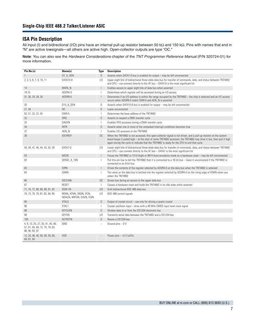
ISA Pin DescriptionAll input (I) and bidirectional (I/O) pins have an internal pull-up resistor between 50 kΩ and 150 kΩ. Pins with names that end in “N” are active lowsignals—all others are active high. Open-collector outputs are type “OC.”
Note: You can also see the Hardware Considerations chapter of the TNT Programmer Reference Manual (P/N 320724-01) for more information.
Pin No.(s) Name(s) Type Description1 D7_0_OEN O Asserts when DATA7-0 bus is enabled for output – may be left unconnected
2, 3, 5, 6, 7, 9, 10, 11 DATA15-8 I/O Upper eight bits of bidirectional three-state data bus for transfer of commands, data, and status between TNT4882and CPU – can connect directly to the AT bus – DATA15 is the most significant bit
14 BHEN_N I Enables access to upper eight bits of data bus when asserted
19-15 ADDR4-0 I Determines which register will be accessed during an I/O access
31, 30, 29, 28, 26 ADDR9-5 I Determines if an I/O address is within the range occupied by the TNT4882 – the chip is selected and an I/O accessoccurs when ADDR9-5 match SW9-5 and AEN_N is asserted
20 D15_8_OEN O Asserts when DATA15:8 bus is enabled for output – may be left unconnected
21, 54 NC O Leave unconnected
52, 51, 23, 22, 55 SW9-5 I Determines the base address of the TNT4882
32 DRQ O Asserts to request a DMA transfer cycle
33 DACKN I Enables FIFO accesses during a DMA transfer cycle
34 INTR O Asserts when one or more of the unmasked interrupt conditions becomes true
37 AEN_N I Enables I/O accesses to the TNT4882
38 IOCHRDY OC When the TNT4882 is not accessed, this open-collector signal is not driven, and a pull-up resistor on the systemboard keeps it pulled high – at the start of some TNT4882 accesses, the TNT4882 may drive it low, then pull it highagain during the cycle to indicate that the TNT4882 is ready for the CPU to end that cycle
50, 49, 47, 46, 44, 43, 42, 39 DATA7-0 I/O Lower eight bits of bidirectional three-state data bus for transfer of commands, data, and status between TNT4882and CPU – can connect directly to the AT bus – DATA7 is the most significant bit
53 MODE I Forces the TNT4882 to 7210 (high) or 9914 (low) emulation mode on a hardware reset – may be left unconnected
62 SENSE_8_16N I Pull this pin low to tell the TNT4882 that it is connected to a 16-bit bus – leave it unconnected if the TNT4882 isconnected to an 8-bit bus
63 IORN I Drives the contents of the register selected by ADDR4-0 on the data bus when the TNT4882 is selected
64 IOWN I The value on the data bus is latched into the register selected by ADDR4-0 on the rising edge of IOWN when youselect the TNT4882
66 IOCS16N OC Driven low during an access to the upper data bus
67 RESET I Causes a hardware reset and holds the TNT4882 in its idle state while asserted
71, 74, 77, 80, 88, 89, 91, 92 DIO8-1N I/O 8-bit bidirectional IEEE 488 data bus
70, 73, 76, 79, 81, 82, 84, 85 RENN, ATNN, SRQN, IFCN,NDACN, NRFDN, DAVN, EOIN
I/O IEEE 488 control signals
95 XTAL0 O Output of crystal circuit – use only for driving a quartz crystal
96 XTAL1 I Crystal oscillator input – drive with a 40 MHz CMOS input level clock signal
98 KEYCLKN O Strobes data to or from the DS1204 electronic key
99 KEYDQ I/O Transmits serial data between the TNT4882 and a DS1204 key
100 KEYRSTN O Resets a DS1204 key
4, 8, 13, 25, 27, 35, 41, 45, 48,57, 61, 65, 68, 72, 75, 78, 83, 86, 90, 93, 97
GND – Ground pins – 0 V
12, 24, 36, 40, 56, 58, 59, 60, 69, 87, 94
VDD – Power pins – +5 V (±5%)
Single-Chip IEEE 488.2 Talker/Listener ASIC
8BUY ONLINE at ni.com or CALL (800) 813 3693 (U.S.)
ISA Pin Description
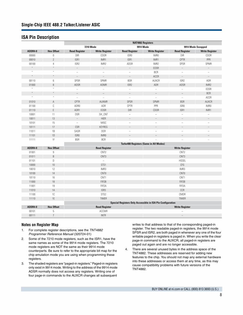
Notes on Register Map1. For complete register descriptions, see the TNT4882
Programmer Reference Manual (320724-01)
2. Some of the 7210 mode registers, such as the ISR1, have the same names as some of the 9914 mode registers. The 7210 mode registers are NOT the same as their 9914 mode counterparts. Be sure to refer to the appropriate bit map for the chip emulation mode you are using when programming these registers.
3. The shaded registers are “paged-in registers.” Paged-in registers only exist in 9914 mode. Writing to the address of the 9914 mode ADSR normally does not access any registers. Writing one of four page-in commands to the AUXCR changes all subsequent
writes to that address to that of the corresponding paged-in register. The two readable paged-in registers, the 9914 mode SPSR and ISR2, are both paged in whenever any one of the four writable paged-in registers is paged in. When you write the clear page-in command to the AUXCR, all paged-in registers are paged out again and are no longer accessible.
4. There are several unused bytes in the address space of the TNT4882. These addresses are reserved for adding new features to the chip. You should not map any external hardware into these addresses or access them at any time, as this may cause compatibility problems with future versions of the TNT4882.
NAT4882 Registers7210 Mode 9914 Mode 9914 Mode Swapped
ADDR4-0 Hex Offset Read Register Write Register Read Register Write Register Read Register Write Register00000 0 DIR CDOR ISR0 IMR0 DIR CDOR
00010 2 ISR1 IMR1 ISR1 IMR1 CPTR PPR
00100 4 ISR2 IMR2 ADSR IMR2 SPSR SPMR
“ “ – – – EOSR – –
“ “ – – – BCR – –
“ “ – – – ACCR – –
00110 6 SPSR SPMR BSR AUXCR ISR2 ADR
01000 8 ADSR ADMR ISR2 ADR ADSR IMR2
“ “ – – – – – EOSR
“ “ – – – – – BCR
“ “ – – – – – ACCR
01010 A CPTR AUXMR SPSR SPMR BSR AUXCR
01100 C ADR0 ADR CPTR PPR ISR0 IMR0
01110 E ADR1 EOSR DIR CDOR ISR1 IMR1
10001 11 DSR SH_CNT – – – –
10011 13 – HIER – – – –
10101 15 – MISC – – – –
10111 17 CSR KEYREG – – – –
11011 1B SASR DCR – – – –
11101 1D ISR0 IMR0 – – – –
11111 1F BSR BCR – – – –
Turbo488 Registers (Same in All Modes)ADDR4-0 Hex Offset Read Register Write Register
01001 9 CNT2 CNT2
01011 B CNT3 CNT3
01101 D – HSSEL
10000 10 STS1 CFG
10010 12 IMR3 IMR3
10100 14 CNT0 CNT0
10110 16 CNT1 CNT1
11000 18 FIFOB FIFOB
11001 19 FIFOA FIFOA
11010 1A ISR3 CCR
11100 1C STS2 CMDR
11110 1E TIMER TIMER
Special Registers Only Accessible in ISA Pin ConfigurationADDR4-0 Hex Offset Read Register Write Register
00101 5 ACCWR –
00111 7 INTR –
Single-Chip IEEE 488.2 Talker/Listener ASIC
9BUY ONLINE at ni.com or CALL (800) 813 3693 (U.S.)
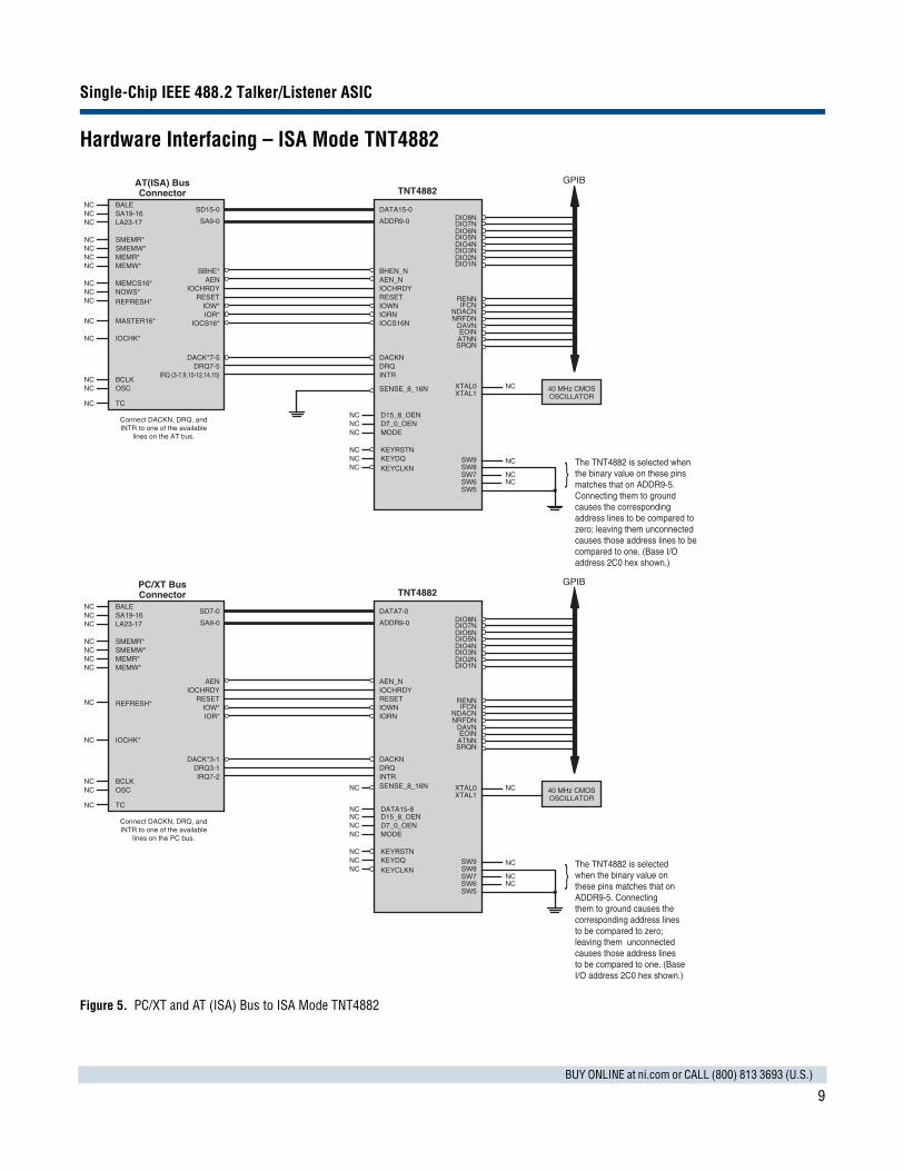
Hardware Interfacing – ISA Mode TNT4882
Figure 5. PC/XT and AT (ISA) Bus to ISA Mode TNT4882
NC
AT(ISA) BusConnector TNT4882
DIO7N
DIO1N
GPIB
NDACNIFCN
NCNC
NCNCNCNC
NCNCNC
NC
NC
NCNC
NC
BALESA19-16LA23-17
SMEMR*SMEMW*MEMR*MEMW*
MEMCS16*NOWS*REFRESH*
MASTER16*
IOCHK*
BCLKOSC
TC
Connect DACKN, DRQ, andINTR to one of the available
lines on the AT bus.
SD15-0
SA9-0
SBHE*AEN
IOCHRDYRESET
IOW*IOR*
IOCS16*
DACK*7-5DRQ7-5
IRQ (3-7,9,10-12,14,15)
DATA15-0
ADDR9-0
BHEN_NAEN_NIOCHRDYRESETIOWNIORNIOCS16N
DACKNDRQINTR
SENSE_8_16N
NCNCNC
NCNCNC
D15_8_OEND7_0_OENMODE
KEYRSTNKEYDQKEYCLKN
DIO8N
DIO2NDIO3NDIO4NDIO5NDIO6N
RENN
NRFDNDAVNEOINATNNSRQN
40 MHz CMOSOSCILLATOR
XTAL0XTAL1
SW9SW8SW7SW6SW5
NC
NC
NCNC }
The TNT4882 is selected when the binary value on these pins matches that on ADDR9-5. Connecting them to ground causes the corresponding address lines to be compared to zero; leaving them unconnected causes those address lines to becompared to one. (Base I/O address 2C0 hex shown.)
NC
PC/XT BusConnector TNT4882
DIO7N
DIO1N
GPIB
NDACNIFCN
NCNC
NCNCNCNC
NC
NC
NCNC
NC
BALESA19-16LA23-17
SMEMR*SMEMW*MEMR*MEMW*
REFRESH*
IOCHK*
BCLKOSC
TC
Connect DACKN, DRQ, andINTR to one of the available
lines on the PC bus.
SD7-0
SA9-0
AENIOCHRDY
RESETIOW*IOR*
DACK*3-1DRQ3-1IRQ7-2
DATA7-0
ADDR9-0
AEN_NIOCHRDYRESETIOWNIORN
DACKNDRQINTRSENSE_8_16N
NCNCNC
NCNCNC
D15_8_OEND7_0_OENMODE
KEYRSTNKEYDQKEYCLKN
DIO8N
DIO2NDIO3NDIO4NDIO5NDIO6N
RENN
NRFDNDAVNEOINATNNSRQN
40 MHz CMOSOSCILLATOR
XTAL0XTAL1
SW9SW8SW7SW6SW5
NC
NC
NCNC }
The TNT4882 is selected when the binary value on these pins matches that onADDR9-5. Connectingthem to ground causes the corresponding address lines to be compared to zero; leaving them unconnected causes those address lines to be compared to one. (BaseI/O address 2C0 hex shown.)
NC
NC DATA15-8
Single-Chip IEEE 488.2 Talker/Listener ASIC
10BUY ONLINE at ni.com or CALL (800) 813 3693 (U.S.)
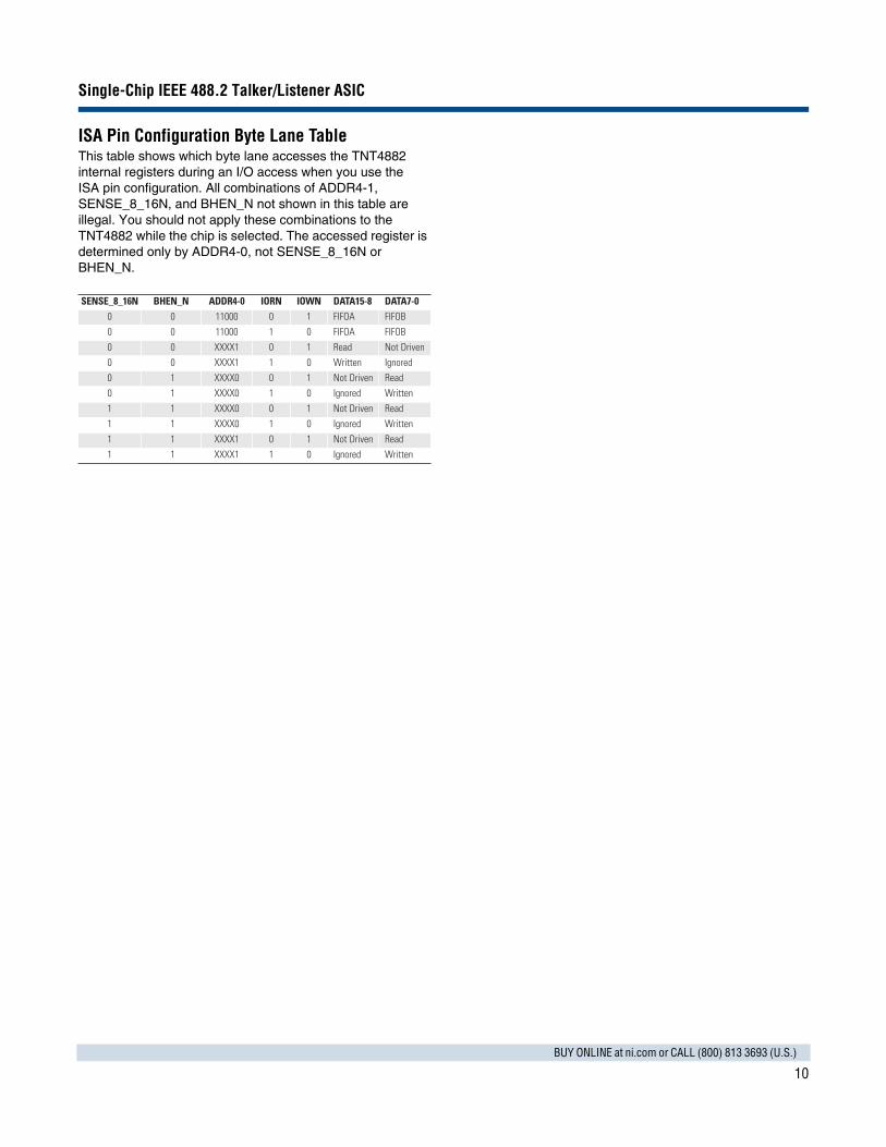
ISA Pin Configuration Byte Lane TableThis table shows which byte lane accesses the TNT4882 internal registers during an I/O access when you use the ISA pin configuration. All combinations of ADDR4-1, SENSE_8_16N, and BHEN_N not shown in this table are illegal. You should not apply these combinations to the TNT4882 while the chip is selected. The accessed register is determined only by ADDR4-0, not SENSE_8_16N or BHEN_N.
SENSE_8_16N BHEN_N ADDR4-0 IORN IOWN DATA15-8 DATA7-00 0 11000 0 1 FIFOA FIFOB
0 0 11000 1 0 FIFOA FIFOB
0 0 XXXX1 0 1 Read Not Driven
0 0 XXXX1 1 0 Written Ignored
0 1 XXXX0 0 1 Not Driven Read
0 1 XXXX0 1 0 Ignored Written
1 1 XXXX0 0 1 Not Driven Read
1 1 XXXX0 1 0 Ignored Written
1 1 XXXX1 0 1 Not Driven Read
1 1 XXXX1 1 0 Ignored Written
Single-Chip IEEE 488.2 Talker/Listener ASIC
11BUY ONLINE at ni.com or CALL (800) 813 3693 (U.S.)
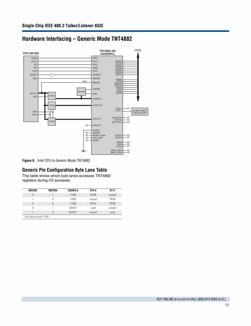
Hardware Interfacing – Generic Mode TNT4882
Figure 6. Intel CPU to Generic Mode TNT4882
Generic Pin Configuration Byte Lane TableThis table shows which byte lanes accesses TNT4882 registers during I/O accesses.
74245
CPU (80186)TNT4882-AQ(GENERIC)
GPIB
74573
NC
NCNCNCNC
NC
40 MHz CMOSOSCILLATOR
NC
NCNCNC
DIO8NDIO7NDIO6NDIO5NDIO4NDIO3NDIO2NDIO1N
RENN
NDACNNRFDN
DAVNEOINATNNSRQN
IFCN
XTAL0XTAL1
KEYRSTNKEYDQ
KEYCLKN
TADCSLADCS
REMTRIG
DCAS
ABUS_OENBBUS_OEN
NC
NCNC
NCNCNC
AD0
DRQ
WRN
DACKN
DATA7-0
RESETN
BBUSN
ADDR4-0
ABUSN
INTR
CSN
CPUACC
PAGEDSWAPNBURST_RDNFIFO_RDYMODE
RDN
RDY1
DATA15-8
DRQ0
ARDY
RD
BHE
INT0
ALE
DEN
AD15-0
WR
RESET
DT/R
73245
Decode
ABUSN BBUSN ADDR4-0 D15-8 D7-00 1 11000 FIFOB unused
1 0 11000 unused FIFOB
0 0 11000 FIFOA FIFOB
0 1 XXXXX1 used unused
1 0 XXXXX1 unused used1Any address except 11000
Single-Chip IEEE 488.2 Talker/Listener ASIC
12BUY ONLINE at ni.com or CALL (800) 813 3693 (U.S.)
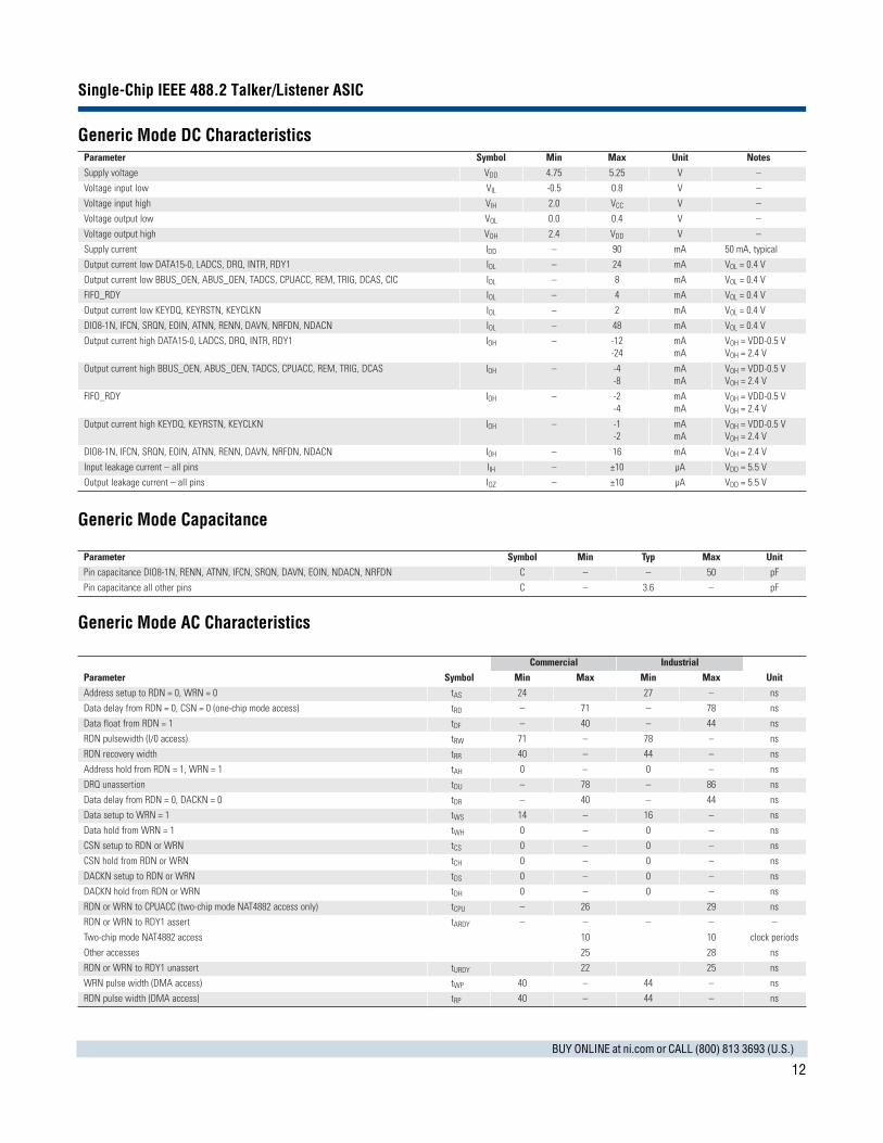
Generic Mode DC Characteristics
Generic Mode Capacitance
Generic Mode AC Characteristics
Parameter Symbol Min Max Unit NotesSupply voltage VDD 4.75 5.25 V –
Voltage input low VIL -0.5 0.8 V –
Voltage input high VIH 2.0 VCC V –
Voltage output low VOL 0.0 0.4 V –
Voltage output high VOH 2.4 VDD V –
Supply current IDD – 90 mA 50 mA, typical
Output current low DATA15-0, LADCS, DRQ, INTR, RDY1 IOL – 24 mA VOL = 0.4 V
Output current low BBUS_OEN, ABUS_OEN, TADCS, CPUACC, REM, TRIG, DCAS, CIC IOL – 8 mA VOL = 0.4 V
FIFO_RDY IOL – 4 mA VOL = 0.4 V
Output current low KEYDQ, KEYRSTN, KEYCLKN IOL – 2 mA VOL = 0.4 V
DIO8-1N, IFCN, SRQN, EOIN, ATNN, RENN, DAVN, NRFDN, NDACN IOL – 48 mA VOL = 0.4 V
Output current high DATA15-0, LADCS, DRQ, INTR, RDY1 IOH – -12-24
mAmA
VOH = VDD-0.5 VVOH = 2.4 V
Output current high BBUS_OEN, ABUS_OEN, TADCS, CPUACC, REM, TRIG, DCAS IOH – -4-8
mAmA
VOH = VDD-0.5 VVOH = 2.4 V
FIFO_RDY IOH – -2-4
mAmA
VOH = VDD-0.5 VVOH = 2.4 V
Output current high KEYDQ, KEYRSTN, KEYCLKN IOH – -1-2
mAmA
VOH = VDD-0.5 VVOH = 2.4 V
DIO8-1N, IFCN, SRQN, EOIN, ATNN, RENN, DAVN, NRFDN, NDACN IOH – 16 mA VOH = 2.4 V
Input leakage current – all pins IIH – ±10 µA VDD = 5.5 V
Output leakage current – all pins IOZ – ±10 µA VDD = 5.5 V
Parameter Symbol Min Typ Max UnitPin capacitance DIO8-1N, RENN, ATNN, IFCN, SRQN, DAVN, EOIN, NDACN, NRFDN C – – 50 pF
Pin capacitance all other pins C – 3.6 – pF
Commercial IndustrialParameter Symbol Min Max Min Max UnitAddress setup to RDN = 0, WRN = 0 tAS 24 27 – ns
Data delay from RDN = 0, CSN = 0 (one-chip mode access) tRD – 71 – 78 ns
Data float from RDN = 1 tDF – 40 – 44 ns
RDN pulsewidth (I/0 access) tRW 71 – 78 – ns
RDN recovery width tRR 40 – 44 – ns
Address hold from RDN = 1, WRN = 1 tAH 0 – 0 – ns
DRQ unassertion tDU – 78 – 86 ns
Data delay from RDN = 0, DACKN = 0 tDR – 40 – 44 ns
Data setup to WRN = 1 tWS 14 – 16 – ns
Data hold from WRN = 1 tWH 0 – 0 – ns
CSN setup to RDN or WRN tCS 0 – 0 – ns
CSN hold from RDN or WRN tCH 0 – 0 – ns
DACKN setup to RDN or WRN tDS 0 – 0 – ns
DACKN hold from RDN or WRN tDH 0 – 0 – ns
RDN or WRN to CPUACC (two-chip mode NAT4882 access only) tCPU – 26 29 ns
RDN or WRN to RDY1 assert tARDY – – – – –
Two-chip mode NAT4882 access 10 10 clock periods
Other accesses 25 28 ns
RDN or WRN to RDY1 unassert tURDY 22 25 ns
WRN pulse width (DMA access) tWP 40 – 44 – ns
RDN pulse width (DMA access) tRP 40 – 44 – ns
Single-Chip IEEE 488.2 Talker/Listener ASIC
13BUY ONLINE at ni.com or CALL (800) 813 3693 (U.S.)
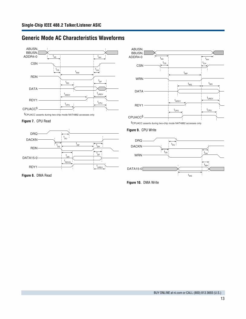
Generic Mode AC Characteristics Waveforms
Figure 7. CPU Read
Figure 8. DMA Read
Figure 9. CPU Write
Figure 10. DMA Write
ABUSN, BBUSN,ADDR4-0 t
AS tAH
CSN
tCS
tCH
RDN
DATA
tDFt
RD
tURDY
tCPU
tARDY
tRW
tCPU
RDY1
CPUACC§
§CPUACC asserts during two-chip mode NAT4882 accesses only
DRQ
DACKN
RDN
DATA15-0
tDU
tDR
tDS
tDH
tDF
RDY1
tRDYQ
tURDY
tRP
DATA
WRN
CSN
ABUSN,BBUSN,
ADDR4-0 tAS
tCS
tWH
tCH
tAH
tWS
tWP
tCPU
tURDYtARDY
tCPU
RDY1
CPUACC§
§CPUACC asserts during two-chip mode NAT4882 accesses only
WRN
DRQ
DACKN
DATA15-0
tWS
tWH
tDU
tDS tDH
Single-Chip IEEE 488.2 Talker/Listener ASIC
14BUY ONLINE at ni.com or CALL (800) 813 3693 (U.S.)
ISA Mode DC Characteristics
ISA Mode Capacitance
Parameter Symbol Min Max Unit NotesSupply voltage VDD 4.75 5.25 V –
Voltage input low VIL -0.5 0.8 V –
Voltage input high VIH 2.0 VCC V –
Voltage output low VOL 0.0 0.4 V –
Voltage output high VOH 2.4 VDD V –
Supply current IDD – 90 mA 50 mA, typical
Output current low DATA15-0, DRQ, INTR, IOCS16, IOCHRDY IOL – 24 mA VOL = 0.4 V
Output current low D7_0_OEN IOL – 16 mA VOL = 0.4 V
Output current low D15_8_OEN, TP_INTWTN IOL – 8 mA VOL = 0.4 V
Output current low KEYDQ, KEYRSTN, KEYCLKN IOL – 2 mA VOL = 0.4 V
Output current low DIO8-1N, RENN, ATNN, IFCN, SRQN, DAVN, EOIN, NDACN, NRFDN IOL – 48 mA VOL = 0.4 V
Output current highDATA15-0, DRQ, INTR
IOH – -12-24
mAmA
VOH = VDD-0.5 VVOH = 2.4 V
Output current highD7_0_OEN
IOH – -8-16
mAmA
VOH = VDD-0.5 VVOH = 2.4 V
Output current highD15_8_OEN, TP_INTWTN
IOH – -4-8
mAmA
VOH = VDD-0.5 VVOH = 2.4 V
Output current highKEYDQ, KEYRSTN, KEYCLKN
IOH – -1-2
mAmA
VOH = VDD-0.5 VVOH = 2.4 V
Output current high DIO8-1N, RENN, ATNN, IFCN, SRQN, DAVN, EOIN, NDACN, NRFDN IOH – -16 mA VOH = 2.4 V
Input leakage current – all pins IIH – ±10 mA VDD = 5.5 V
Output leakage current – all pins IOZ – ±10 mA VDD = 5.5 V
Parameter Symbol Min Typ Max UnitPin capacitance DATA15-0, DRQ, INTR, IOCS16N, IOCHRDY, ADDR6 C – 3.6 – pF
Pin capacitance D7_0_OEN, D15_8_OEN, TP_INTWTN, KEYDQ, KEYRSTN, KEYCLKN, ADDR4, ADDR8, ADDR9 C – 3.0 – pF
Pin capacitance BHEN_N, ADDR3-0, ADDR5, ADDR7, DACKN, AEN_N, MODE, TESTMODE, PWBSEL2-0, SW9,SENSE_8_16N, IORN, IOWN, RESET
C – 3.5 – pF
Pin capacitance DIO8-1N, RENN, ATNN, IFCN, SRQN, DAVN, EOIN, NDACN, NRFDN C – – 50 pF
Single-Chip IEEE 488.2 Talker/Listener ASIC
15BUY ONLINE at ni.com or CALL (800) 813 3693 (U.S.)
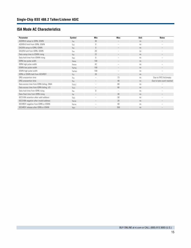
ISA Mode AC Characteristics
Parameter Symbol Min Max Unit NotesADDR9-0 setup to IORN, IOWN tAS 30 – ns –
ADDR9-0 hold from IORN, IOWN tAH 0 – ns –
DACKN setup to IORN, IOWN tDS 0 – ns –
DACKN hold from IORN, IOWN tDH 20 – ns –
Data setup time to IOWN rising tSU 22 – ns –
Data hold time from IOWN rising tWH 0 – ns –
IORN low pulse width tRPWL 100 – ns –
IORN high pulse width tRPWH 42 – ns –
IOWN low pulse width tWPWL 100 – ns –
IOWN high pulse width tWPWH 100 – ns –
IORN or IOWN held from IOCHRDY tTD 20 – ns –
DRQ unassertion time tDU – 73 ns Due to FIFO full/empty
DRQ unassertion time tDU – 48 ns Due to byte count reached
Data access time from IORN falling, DMA tDACC – 80 ns –
Data access time from IORN falling, I/O tACC – 80 ns –
Data hold time from IORN rising tRH 0 – ns –
Data float time from IORN rising tDF – 30 ns –
IOCS16N assertion after valid address tDEC – 30 ns –
IOCS16N negation after invalid address tDECN – 20 ns –
IOCHRDY negation from IORN or IOWN tRDYN – 40 ns –
IOCHRDY release after IORN or IOWN tRDY – 350 ns –
Single-Chip IEEE 488.2 Talker/Listener ASIC
16BUY ONLINE at ni.com or CALL (800) 813 3693 (U.S.)
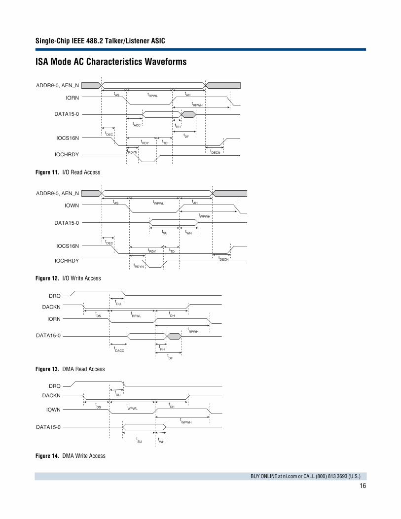
ISA Mode AC Characteristics Waveforms
Figure 11. I/O Read Access
Figure 12. I/O Write Access
Figure 13. DMA Read Access
Figure 14. DMA Write Access
ADDR9-0, AEN_N
IORN
DATA15-0
IOCS16N
IOCHRDY
tAH
tRH
tDF
tDECN
tTDtRDY
tRDYN
tACC
tDEC
tAS tRPWL
tRPWH
ADDR9-0, AEN_N
IOWN
DATA15-0
IOCS16N
IOCHRDY
tAH
tDECN
tTDtRDY
tRDYN
tDEC
tAS tWPWL
tWPWH
tWHtSU
IORN
DRQ
DACKN
DATA15-0
tDF
tRH
tDU
tDS
tDH
tRPWH
tDACC
tRPWL
IOWN
DRQ
DACKN
DATA15-0
tWH
tDU
tDS
tDH
tWPWH
tWPWL
tSU
Single-Chip IEEE 488.2 Talker/Listener ASIC
17BUY ONLINE at ni.com or CALL (800) 813 3693 (U.S.)
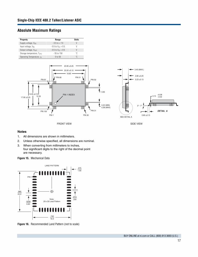
Absolute Maximum Ratings
Notes1. All dimensions are shown in millimeters.
2. Unless otherwise specified, all dimensions are nominal.
3. When converting from millimeters to inches, four significant digits to the right of the decimal point are necessary.
Figure 15. Mechanical Data
Figure 16. Recommended Land Pattern (not to scale)
18.85
PIN 1 INDEX
WEIVEDISWEIVTNORF
PIN 1 PIN 30
PIN 31
PIN 51PIN 50
PIN 80PIN 81
PIN 100
20.00 ±0.10
23.90 ±0.25
0.65
0.22 (MIN)0.38 (MAX)
12.3514.00 ±0.10
17.90 ±0.25
3.40 (MAX.)
2.80 ±0.25
0.23 ±0.13
SEE DETAIL A
DETAIL A
0.15 +0.08–0.02
0° –7°
0.80 ±0.15
Property Range UnitsSupply voltage, VDD - 0.5 to + 7.0 V
Input voltage, VIN - 0.5 to VCC + 0.5 V
Output voltage, VOUT - 0.5 to VCC + 0.5 V
Storage temperature, TSTG - 55 to 150 ˚C
Operating Temperature, TA 0 to 50 ˚C
Note:20 x 30 Lead Pattern
LAND PATTERN.0751.90
.013
.330
.74518.9
.02560.65
.98024.9
PIN 1
National Instruments, NI, ni.com, and LabVIEW are trademarks of National Instruments Corporation. Refer to the Terms of Use section on ni.com/legal for more information about National Instruments trademarks. Other product and company names mentioned herein are trademarks or trade names of their respective companies. A National Instruments Alliance Partner is a business entity independent from NI and has no agency, partnership, or joint-venture relationship with NI.
© 1999–2006 National Instruments Corporation. All rights reserved. 372014B-01 Sep06
NI Services and Support
NI has the services and support to meet your needs around the globe and through the application life cycle – from planning and development through deployment and ongoing maintenance. We offer services and service levels to meet customer requirements in research, design, validation, and manufacturing. Visit ni.com/services.
Training and CertificationNI training is the fastest, most certain route to productivity with our products. NI training can shorten your learning curve, save development time, and reduce maintenance costs over the application life cycle. We schedule instructor-led courses in cities worldwide, or we can hold a course at your facility. We also offer a professional certification program that identifies individuals who have high levels of skill and knowledge on using NI products. Visit ni.com/training.
Professional ServicesOur Professional Services Team is comprised of NI applications engineers, NI Consulting Services, and a worldwide National Instruments Alliance Partner program of more than 600 independent consultants and integrators.
Services range from start-up assistance to turnkey system integration. Visit ni.com/alliance.
OEM SupportWe offer design-in consulting and product integration assistance if you want to use our products for OEM applications. For information about special pricing and services for OEM customers, visit ni.com/oem.
Local Sales and Technical SupportIn offices worldwide, our staff is local to the country, giving you access to engineers who speak your language. NI delivers industry-leading technical support through online knowledge bases, our applications engineers, and access to 14,000 measurement and automation professionals within NI Developer Exchange forums. Find immediate answers to your questions at ni.com/support.
We also offer service programs that provide automatic upgrades to your application development environment and higher levels of technical support. Visit ni.com/ssp.
Hardware ServicesNI Factory Installation ServicesNI Factory Installation Services (FIS) is the fastest and easiest way to use your PXI or PXI/SCXI combination systems right out of the box. Trained NI technicians install the software and hardware and configure the system to your specifications. NI extends the standard warranty by one year on hardware components (controllers, chassis, modules) purchased with FIS. To use FIS, simply configure your system online with ni.com/pxiadvisor.
Calibration ServicesNI recognizes the need to maintain properly calibrated devices for high-accuracy measurements. We provide manual calibration procedures, services to recalibrate your products, and automated calibration software specifically designed for use by metrology laboratories. Visit ni.com/calibration.
Repair and Extended WarrantyNI provides complete repair services for our products. Express repair and advance replacement services are also available. We offer extended warranties to help you meet project life-cycle requirements. Visit ni.com/services.
CUSTOMER NEEDS