
Re-programming the Simon Says with Arduino Linz Craig, Brian Huang.

Simon SaysFinal Project ReportDecember 9, 1999
E157
David Honeycutt and Jerry Kurtze
Abstract:
Simon Says is a simple game in which three lights are lit up in a random pattern beginning with one entryand a player is asked to repeat the pattern. Upon successful repetition of the pattern, the pattern length isincreased by one and the player is again asked to repeat the pattern. This project prototypes animplementation of the game Simon Says consisting of a keypad, microcontroller, FPGA and seven-segmentdisplay. When the game begins, the player chooses one of three speeds at which to play. Themicrocontroller accepts this input and generates one random entry for the pattern. It then sends a signal tothe FPGA to light up the corresponding LED, and waits for input from the FPGA, which decodes keypresses on the keypad. Upon successful repetition, the microcontroller generates another random entry forthe pattern and again sends signals to the FPGA to light up the LEDs. The game continues in this fashionuntil the player incorrectly repeats the pattern. When the game ends, a high score is output on a seven-segment display.

2
IntroductionAt the beginning of the final project, we knew that we wanted to make a game. After thinking
about some possibilities for games, we remembered playing Simon Says as kids. We thought about how
the design would work, and decided that Simons Says would be a fun, and manageable project.
The Simon Says game functions as follows. Upon power up, the game waits for the user to press a
speed key before play begins. The three speed keys (discussed below) are labeled on the keypad. Upon
starting, the game turns on one of the LEDs for two seconds (assuming slowest speed), turns it back off,
and wait for the user to repeat this pattern by pushing one of the colored buttons on the keypad. If the
player does this successfully, the game continues. The same first LED turns on for two seconds, then turns
off. Next, a second LED turns on for two seconds, then turns off, and again the game waits for the player
to repeat the pattern of LEDs lit by pushing buttons on the keypad. The game continues, adding one more
LED to the pattern, until the player incorrectly repeats the pattern of LEDs lit. The pattern of LEDs lit is
random and unique for each game.
When the game ends, the seven-segment display outputs the high score, which is updated if the
game that just ended had the largest sequence of LEDs since the game was turned on. The seven-segment
display maintains its output until a new game is started. There are also be three speed keys on the keypad.
The user selects the speed of game play by pushing one of the speed keys. Once a speed key is pressed, the
game automatically begins. The player can begin another game by pushing one of the speed buttons after
the game ends.
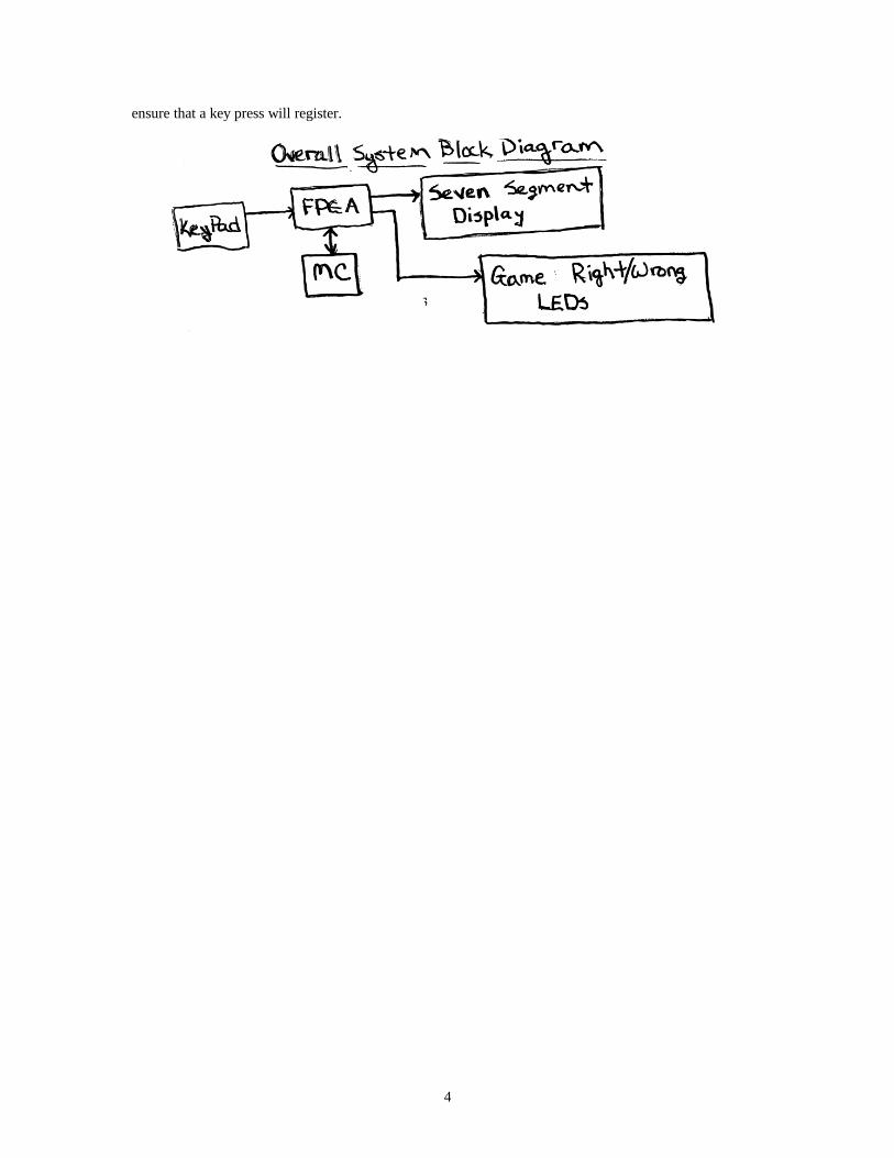
Main Subsystems & Division between FPGA and Microprocessor:
The FPGA is used for glue logic and driving both the seven-segment display and the LEDs. The
microcontroller is used to control the flow of the program and to make calculations. A block diagram of
the overall system is included on page 4. The following is a breakdown of the functions for the FPGA and
the microcontroller:
FPGA• Debounce and Interpret Key pad presses & Send decoded signal to the MC• Send signals to 3 game LEDs (controlled by microcontroller)• Output high score to seven segment display (high score sent from microcontroller)• Create clock signal for speed of game (sent to microcontroller)• Generate random sequence of three numbers to be sent to microcontroller
3
• Drives correct and incorrect answer LEDs
Microcontroller• Controls overall flow of game play• Generates new LED to add to pattern based on random number polled from the FPGA• Check keypad inputs sent from FPGA against table in stack• Keeps track of high score• Controls game LED light-up and associated timing• Controls correct/incorrect LEDs
In addition to the logic included in the FPGA and microcontroller, there is some use of logic on the
breadboard to drive the seven-segment display and the keyboard. The seven-segment display is
multiplexed using two transistors. By using a clock and a not of the same clock, it is possible to use the
transistors and seven outputs from the FPGA to drive both of the seven-segment displays (each of the seven
outputs from the FPGA drives a single part of the seven segment display). When one clock is high, the
other is low, and thus one transistor is on while the other is off. Therefore, even though both of the seven-
segment displays are receiving the same signal, only one outputs the signal. By alternating the output from
the FPGA at the same speed that the transistors are turned on and off, two signals can be sent out through
the same seven outputs from the FPGA and are displayed separately on each of the seven-segment displays.
The clock used to control this system runs at 2MHz, thus the time that the LEDs are off is undetectable by
the naked eye.
The keypad functions by using the concept of polling. Four pins are sequentially polled, one pin
receiving a low signal while the other three pins receive a high signal. The low signal continuously
switches from one input pin to the next. When a key is pressed, one of the output pins from the keypad will
be pulled low when the corresponding input pin receiving a low is connected to this output pin. By locking
the polling when this happens, you can determine exactly which button was pressed by knowing which
input pin is low and which output pin is pulled low. There are resistors connected to the output pins and
Vcc, which pull the output pins high in all other cases. It is important to be sure the polling is fast enough to
4
ensure that a key press will register.
5
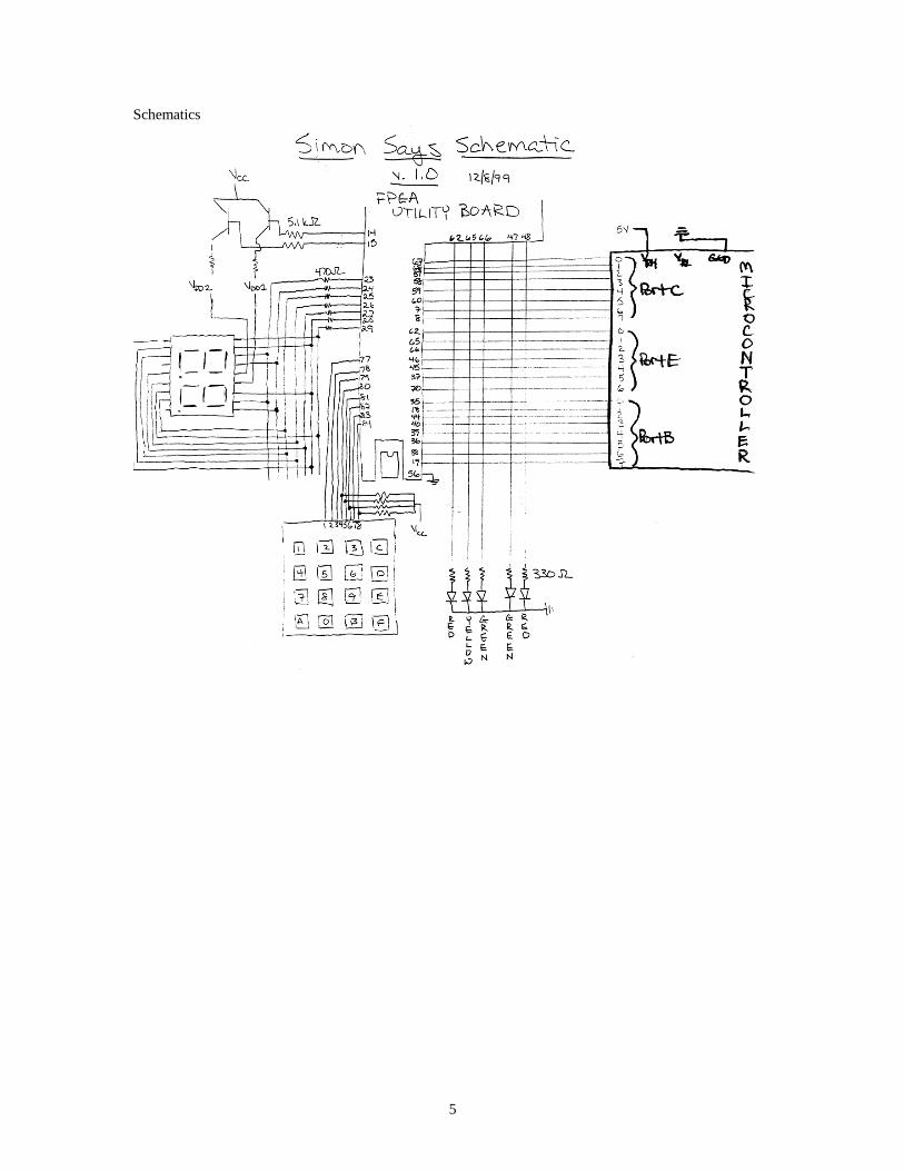
Schematics
6
Microcontroller DesignThe following is a description of the major software modules in the microcontroller. A detailed
description of the inputs and outputs of the microcontroller are included in a table below. Ourmicrocontroller code is included in the appendix. The major modules of the microcontroller are as follows:
Modules for Microcontroller:• Set speed• Create new LED for sequence• Check user’s input sequence against stack• Output high score
The following is a description of how the microcontroller functions:
Function of Microcontroller:
1) Initialize Port C and Declare Variable Names for Memory Locations
2) Clear Memory Locations
3) Loop to Monitor Port C and wait for a speed key to be pressed. Based on signal received, themicrocontroller sends a signal to Port B to a MUX in the FPGA and beings to receive the appropriateclock signal.
4) Initialize stack by setting stack pointer, clear registers and Port E5) Poll input from FPGA to acquire random number for new LED, add new LED to stack, and update
level6) Output sequence to FPGA using the timer input from the FPGA and the stack values stored7) Loop to monitor Port E waiting for input from the player. Check each key press against stack. If
incorrect goto Step 8. If whole sequence is repeated correctly, goto Step 58) Compare high score with last correctly completed level and change high score if necessary. Goto step
3.
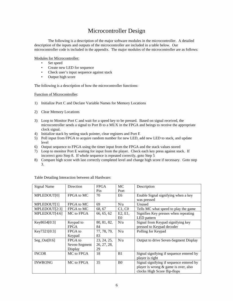
Table Detailing Interaction between all Hardware:
Signal Name Direction FPGAPin
MCPort
Description
MPLEDOUT[0] FPGA to MC 70 E6 Enable Signal signifying when a keywas pressed
MPLEDOUT[1] FPGA to MC 69 N/a UnusedMPLEDOUT[2:3] FPGA to MC 68, 67 C1, C0 Tells MC what speed to play the gameMPLEDOUT[4:6] MC to FPGA 66, 65, 62 E2, E1,
E0Signifies Key presses when repeatingLED pattern
Key8654[0:3] Keypad toFPGA
80, 81, 82,84
N/a Signal from Keypad signifying keypressed to Keypad decoder
Key7321[0:3] FPGA toKeypad
77, 78, 79,83
N/a Polling for Keypad
Seg_Out[0:6] FPGA toSeven-SegmentDisplay
23, 24, 25,26, 27, 28,29
N/a Output to drive Seven-Segment Display
INCOR MC to FPGA 18 B1 Signal signifying if sequence entered byplayer is right
INWRONG MC to FPGA 35 B0 Signal signifying if sequence entered byplayer is wrong & game is over, alsoclocks High Score flip-flops

7
OUTCOR FPGA to GreenLED
47 N/a Signal to drive LED (FPGA used asbuffer)
OUTWRONG FPGA to RedLED
48 N/a Signal to drive LED (FPGA used asbuffer)
Rand_Out[0:1] FPGA to MC 45, 46 E4, E3 Microcontroller polls this signal toproduce new LED for pattern
SEL_LED MC to FPGA38
B6 Select bit for Mux controlling if LEDsare driven by User Key Presses or MCpattern output
NEWPAT[0:2] MC to FPGA 39, 40, 44 B4, B3,B2
Signal to LEDs to output sequence
LEDOUTCLK FPGA to MC 37 E5 Clock sent to MC to control game speedLEDCLKSEL[0:1] MC to FPGA 19, 36 B7, B5 Tells the FPGA which clock to send to
MC for game speed (select of MUX)HISCORE[0:5] MC to FPGA 57, 58, 59,
60, 7, 8C2, C3,C4, C5,C6, C7
Outputs high score to FPGA

8
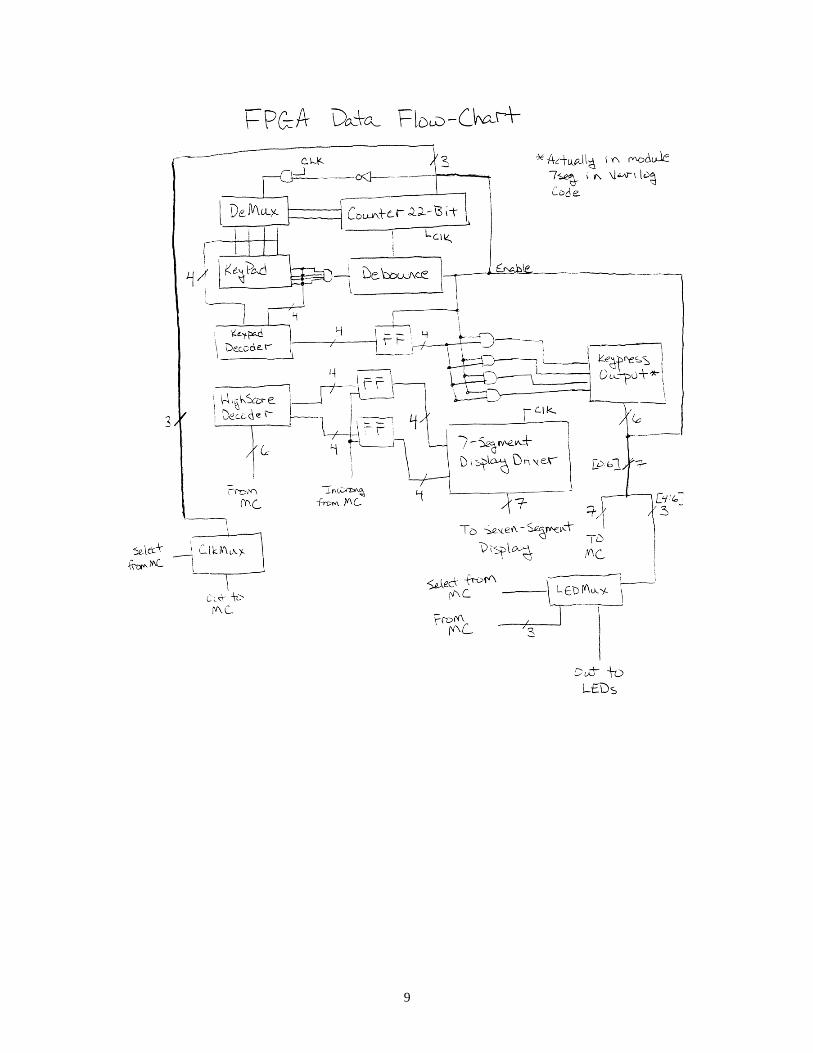
FPGA DesignAs stated in the introduction, the FPGA is used for glue logic and driving both the seven-segment
display and the LEDs. The table included in the Microcontroller Design section details the inputs andoutputs of the FPGA. The following is a description of all the modules used in the FPGA. A data flowchart for the FPGA is included on the next page .
Description of Modules in FPGA:
Top Level:The top level module wires all the other modules together as seen on page X.22 Bit Counter:This module provides a delayed clock to the MC for game play speed, as well as a delayed clock for thedebouncer and the MUX used for polling the keypad.1x4 DeMux:MUX used for polling the keypad.Debouncer:The debouncer is used to debounce the signal from the keypad to ensure that each key press is onlyinterpreted once.Keyboard Decoder:This decodes the signal sent from the key pad to determine which key was pressed.High Score Decoder:This decodes the high score sent from the MC and sends output to the seven-segment display driver.Flip Flops:We used flip flops in different parts of the overall FPGA hardware design, as seen in the FPGA datapathdiagram below.Seven Segment Display:This module can effectively be divided into two modules: The seven segment display driver and the Keypress Output module.
• The seven segment display module takes input from the High Score Decoder and outputs this tothe seven-segment display.
• The Key Press Output module takes input from the Keypad Decoder and outputs to a MUXcontrolling the game LEDs.
2x3 MUX:This module selects if the microcontroller or key presses on the keypad are displayed on the game LEDs.The select is controlled by the microcontroller.3x1 MUX:This module outputs one of three clocks coming from the 22 bit counter. The select is controlled by themicrocontroller.2 Bit Counter:This module counts the numbers 0, 1 and 2 sequentially, looping back to 0 after 2. This signal is sent to theMC for generating the random pattern of LEDs.
9

10
ResultsWe were able to complete the design and produced a functional version of Simon Says. The only
change we made to our specification is that the available game play speeds are 2s, 1s and 0.5s instead of
1.5s, 1s and 0.5s. We made this change because it reduced the number of output pins necessary on the
FPGA and input pins necessary on the MC.
Microcontroller Problems:
We had to write the software to run the microprocessor (MC) from scratch. Our first step was to
attempt to read signals from the FPGA telling the MC what key had been pressed. The problems we had
with this dealt with the key press signal sent from the FPGA. Our first problem was that, by sending a
control signal that went high when a key was pressed, we could not tell if a colored key was pressed after
the first colored key was pressed. This was because the signal was programmed to be high even after the
key was no longer being pressed. To fix this problem, we used the enable signal from the Debouncer
section of Lab 4. This solved the problem since the enable signal is high for a certain amount of time after
the key is pressed. During our testing with this signal we found that on one key press, our stack would
become full. The MC program was running fast enough, that it could detect one key press as many key
presses. To fix this problem, we created code to only detect a key press on the positive edge of enable, thus
recording the key press only once. Later, we eliminated using the enable signal, since the microcontroller
is running fast enough to detect a key press without the enable signal. By simply looking for a positive
edge on any of the three LED signals from the FGPA, we could detect a key press, and this design was
simpler.
Once we were able to read in key presses, we modified our code to check each key press against a
known pattern that was stored in the stack. In our first attempt to implement the stack, we found that you
cannot use the C### section of the MC memory, and eventually moved the stack to section D### of the
MC memory.
We initially decided to use the interrupt system to control the speed of the game. After
implementing this design, we realized that the interrupt system could run, at its slowest, at a speed of
approximately 16ms. Therefore, we decided to implement a 22-bit counter in the FPGA and output the
three highest bits as clocks to the microcontroller. These bits represent a 2s, 1s and 0.5s clocks. In order to
11
get this implementation to work, we had to MUX the three clocks and send a control signal from the MC to
the FPGA to select the appropriate clock. Using code in the MC to detect positive edges of these clocks,
we were able to control the timing for outputs to the LEDs.
Once we had the system fully implemented, the MC was incorrectly checking key presses against
the stack about 15% of the time. We realized that, in our MC code, we polled Port E twice in a row, using
the first value to know what button was pressed, and the second value to check if a button had been pressed
at all. The problem was that sometimes the button was pressed in-between these two polls of Port E, and
we were detecting a key press without knowing what key had been pressed. By switching the order of
these polls to Port E, we were able to fix the problem.
FPGA Problems:
Originally we had planned to use a Finite State Machine in the FPGA to control the flow of the
game. After considering this decision, we realized it was much easier to have the MC code control of the
game.
In our original implementation of using the signals from the key pad to control the game LEDs,
the LEDs stayed on after the key had been pressed. This was not a good implementation since pressing a
button twice in a row was not visible to the player. We needed to change the implementation so the LED
was on only during the time that the key was held down. In order to achieve this, we AND’ed the enable
signal produced by the debouncer with the output from the Keypad Decoder after it had passed through a
flip-flop. This produced the desired effect.
In our initial design for producing a random number to generate the LED pattern, we used a two
bit counter (the first two bits of the 22-bit counter) to count between 0 and 3. However, this
implementation was not optimal since it required us to find a way to deal with transferring four possible
inputs (0-3) to the three LEDs (red, yellow, green). We decided that it was easier to create a counter that
only counts between 0 and 2, and output this to the MC instead. This made the MC code to convert the
number to a LED press much simpler.
We had the INWRONG signal locked to Pin 50 during all of the early design. However, when we
implemented the High Score input in the FPGA, this created a problem concerning the internal layout of
the FPGA and what pins could and could not be provided a clock signal. After trying many other pins and
12
finding no success, we decided to speak to Professor Harris about the problem. He explained that the
FPGA can provide a clock signal to only some of the pins when the FPGA begins to be full, and it was
necessary for us to find out what pins could support a clock signal. We did this by looking at the .UCF file
produced by Xilinx after locking the device pins and leaving that one pin unlocked so the program would
correctly lock it. Then we opened up the .ucf file to see where the program locked the signal.

13
References[1] Honeycutt & Kurtze, Lab 3: Multiplexed Display, Havey Mudd College, CA: 1999.[2] Honeycutt & Kurtze, Lab 4: Keyboard Encoding, Havey Mudd College, CA: 1999.[3] M68HC11 Reference Manual, USA: Motorola, 1991

14
Appendix A0001 ****************************************0002 *0003 * FINAL PROJECT0004 *0005 ****************************************00060007 ***** Variable Declarations0008 1007 DDRC EQU $10070009 1003 PORTC EQU $10030010 100a PORTE EQU $100A0011 1004 PORTB EQU $10040012 d004 LEVEL EQU $D0040013 d003 NUMBPRESS EQU $D0030014 d007 Z EQU $D0070015 d008 CHECKA EQU $D0080016 d009 CHECKB EQU $D0090017 d00a SPEEDREG EQU $D00A0018 d00b HIGHSCORE EQU $D00B00190020 * Specifies to start writing memory
location $D1000021 d100 ORG $D1000022 0023 * SETS HIGH SCORE TO ZERO0024 d100 86 00 LDAA #$000025 d102 b7 d0 0b STAA HIGHSCORE00260027 *SET PORT C TO RECIEVE INPUT0028 d105 86 fc SPEED LDAA #$FC0029 d107 b7 10 07 STAA DDRC
* Keep only neccessay bits0030 d10a 86 03 LDAA #$030031 d10c b4 10 03 ANDA PORTC
* Branch if speed is not selected0032 d10f 27 f4 BEQ SPEED********************************************************************
* Checks to see what speed is selected********************************************************************00330034 d111 81 01 CMPA #$010035 d113 27 08 BEQ ONE00360037 d115 81 02 CMPA #$020038 d117 27 08 BEQ HALF0039 d119 86 a0 LDAA #$A00040 d11b 20 06 BRA ENDSPD00410042 d11d 86 80 ONE LDAA #$800043 d11f 20 02 BRA ENDSPD00440045 d121 86 20 HALF LDAA #$20004600470048 d123 b7 d0 0a ENDSPD STAA SPEEDREG0049 d126 b7 10 04 STAA PORTB

15
005000510052 *SET UP THE STACK AT D4000053 d129 ce d3 00 LDX #$D3000054 d12c 35 TXS005500560057 d12d 86 00 LDAA #$000058 *INITIALIZE LOCATION FOR BUTTON PRESSED0059 d12f b7 d0 03 STAA NUMBPRESS0060 *INITIALIZE LOCATION FOR NUMBERS OFCURRENT LEVEL0061 d132 b7 d0 04 STAA LEVEL00620063 *CLEARING PORTe0064 d135 c6 00 LDAB #$000065 d137 f7 10 0a STAB PORTE0066 *INITIALIZE MEMORY FOR DUPLICATE KEYPRESS
CHECKING0067 d13a f7 d0 01 STAB $D0010068 d13d f7 d0 02 STAB $D00200690070 * Clear CHECK REGISTERS0071 d140 f7 d0 08 STAB CHECKA0072 d143 f7 d0 09 STAB CHECKB00730074 *REGISTER FOR CREATING RANDOM NUMBER WHEN
INPUT OF $00 IS RECIEVED0075 d146 c6 01 LDAB #$010076 d148 f7 d0 05 STAB $D0050077 0078 00790080 *BRACH TO NEWLED TO CREATE FIRST LED INPUT
FOR THE GAME0081 d14b 20 3b BRA NEWLED00820083 *SECTION TO DECREMENT X UNTIL B IS ZERO0084 d14d 09 DECR DEX0085 d14e 5a DECB0086 d14f 7e d1 72 JMP AGAIN00870088********************************************************0089 * WAITING FOR INPUTS FROM FPGA0090 d152 f6 d0 02 LOOP LDAB $D0020091 *COPY NUMBER IN $D002 to $D0010092 d155 f7 d0 01 STAB $D0010093 *LOAD REG A AND B WITH CONTENTS OF PORTE0094 d158 f6 10 0a LDAB PORTE0095 d15b b6 10 0a LDAA PORTE0096 *GET RID OF ALL BITS BUT 6TH IN B0097 d15e c4 07 ANDB #$070098 *STORE THIS CONTROL BIT FOR KEPRESS
CHECKING LATER0099 d160 f7 d0 02 STAB $D002

16
0100 *BRANCH TO LOOP IF CONTROL BIT LOW SINCE MEANS NOT KEY PRESSED
0101 d163 27 ed BEQ LOOP01020103 *LOAD LAST CONTROL BIT0104 d165 f6 d0 01 LDAB $D0010105 *IF LAST CONTROL BIT IS 0 THEN MEANS THERE
WAS KEYPRESS SO THEN CONTINUE ELSE BRANCH LOOP
0106 d168 26 e8 BNE LOOP010701080109**********************************************************0110 * ONCE WE GET AN INPUT, WE NEED TO DEAL
WITH IT01110112 *KEEP ONLY BITS [0:2]0113 d16a 84 07 ANDA #$070114 d16c ce d2 ff LDX #$D2FF0115 *LOAD BUTTONS PRESSED INTO B0116 d16f f6 d0 03 LDAB NUMBPRESS0117 *GOTO DECREMENT IF BUTTON PRESSED HAS NOT
BEEN FULLY SUBTRACTED FROM X, TO FINISH DECREMENTING
0118 d172 26 d9 AGAIN BNE DECR0119 *SUBTRACT WHAT IS IN X FROM A AND PUT IN A0120 d174 b7 d0 10 STAA $D0100121 d177 a0 00 SUBA 0,X0122 *IF THE NUMBER IN X AND A ARE NOT THE SAME
GO TO INCOR SINCE THE USERS PATTERN WAS WRONG
0123 d179 26 67 BNE INCOR01240125 *LOAD IN THE NUMBER KEYPRESS TO INCREMENT
SINCE A NEW CORRECT KEY WAS INPUTED0126 d17b f6 d0 03 LDAB NUMBPRESS0127 d17e 5c INCB0128 d17f f7 d0 03 STAB NUMBPRESS0129 *LOAD THE CURRENT LEVEL INTO0130 d182 b6 d0 04 LDAA LEVEL0131 d185 10 SBA0132 *IF THE CURRENT LEVEL AND THE NUMBER OF
BUTTONS PRESSED ARE DIFFERENT GOTO LOOP, ELSE CONTINUE
0133 d186 26 ca BNE LOOP013401350136**************************************************************************0137 *NOW SEND OUT SIGNAL TO PORT B TO SIGNIFY
THAT THE CORRECT PATTERN WAS ENTERED0138 *CLEAR NON-IMPORTANT BITS************************************************************************************************** Section for generating next LED for pattern***********************************************************************

17
0139 d188 86 18 NEWLED LDAA #$180140 d18a b4 10 0a ANDA PORTE
* Turns on Green LED cause correct answer
0141 d18d c6 02 LDAB #$02* Keeps the right speed select output to the
FPGA0142 d18f fa d0 0a ORAB SPEEDREG0143 d192 f7 10 04 STAB PORTB01440145 *SHIFT BITS 3 & 4 TO BITS 0 AND 10146 *MUST CLEAR CARRY BIT SO IT DOES NOT GET
SHIFTED IN0147 d195 44 LSRA0148 d196 44 LSRA0149 d197 44 LSRA0150 d198 4c INCA0151 d199 81 03 CMPA #$030152 d19b 26 02 BNE STACK0153 d19d 86 04 LDAA #$04
* Load Number on Stack0154 d19f 36 STACK PSHA
* Increase Level value by one0155 d1a0 b6 d0 04 LDAA LEVEL0156 d1a3 4c INCA0157 d1a4 b7 d0 04 STAA LEVEL0158 d1a7 86 00 LDAA #$000159 *INITIALIZE LOCATION FOR BUTTON PRESSED0160 d1a9 b7 d0 03 STAA NUMBPRESS0161 d1ac b7 d0 06 STAA $D0060162 d1af b7 d0 07 STAA Z0163 d1b2 18 ce d2 ff LDY #$D2FF0164
* Check to see if the user has entered the full sequence yet, if they have
then get newled0165 d1b6 b6 d0 07 CHECK LDAA Z0166 d1b9 4a DECA0167 d1ba b1 d0 04 CMPA LEVEL0168 d1bd 27 18 BEQ OFF0169 ** Check to find posedge clock0170 d1bf f6 d0 08 LOOP2 LDAB CHECKA0171 d1c2 f7 d0 09 STAB CHECKB0172 d1c5 86 20 LDAA #$200173 d1c7 b4 10 0a ANDA PORTE0174 d1ca b7 d0 08 STAA CHECKA0175 d1cd 27 f0 BEQ LOOP20176 d1cf b0 d0 09 SUBA CHECKB0177 d1d2 27 eb BEQ LOOP201780179 **JUMP INTO Output Routine0180 d1d4 7e d2 01 JMP OUT0181
* Turns off all LED Lights0182 d1d7 86 00 OFF LDAA #$00
* Keeps the right speed select output to the FPGA

18
0183 d1d9 ba d0 0a ORAA SPEEDREG0184 d1dc b7 10 04 STAA PORTB0185 d1df 7e d1 52 JMP LOOP01860187*************************************************************************0188 *SEND OUT SIGNAL TO PORT B TO SIGNIFY THAT
THE INCORRECT PATTERN WAS ENTERED0189 d1e2 b6 d0 04 INCOR LDAA LEVEL0190 d1e5 4a DECA
* Check to see if new score is high score if it is write it over old high
score in memory location0191 d1e6 b1 d0 0b CMPA HIGHSCORE0192 d1e9 2d 03 BLT OUTSCRE0193 d1eb b7 d0 0b STAA HIGHSCORE0194 d1ee b6 d0 0b OUTSCRE LDAA HIGHSCORE0195 d1f1 48 LSLA0196 d1f2 48 LSLA
* Write high score to portc0197 d1f3 b7 10 03 STAA PORTC0198
* Turns on Red LED since game over0199 d1f6 c6 01 LDAB #$01
* Keeps the right speed select output to the FPGA
0200 d1f8 fa d0 0a ORAB SPEEDREG0201 d1fb f7 10 04 STAB PORTB
* Go to speed to wait to start game again0202 d1fe 7e d1 05 JMP SPEED020302040205 * OUT ROUTINE***********************************************************************
* This Routine controls the right LEDs being on and off at the right time
***********************************************************************0206 d201 b6 d0 06 OUT LDAA $D0060207 d204 27 17 BEQ LEDOFF
* If last time the LED was off then need to turn one on
0208 d206 18 a6 00 LDAA 0,Y0209 d209 48 LSLA0210 d20a 48 LSLA0211 d20b c6 40 LDAB #$400212 d20d 1b ABA
* Keeps the right speed select output to the FPGA
0213 d20e ba d0 0a ORAA SPEEDREG0214 d211 b7 10 04 STAA PORTB
* Turn off LED0215 d214 86 00 LDAA #$000216 d216 b7 d0 06 STAA $D006
* Now need to point to next place in stack which has the next LED to light up
0217 d219 18 09 DEY

19
0218 d21b 20 14 BRA OUTEND* if last time and LED was on we need to turn
it off0219 d21d 86 40 LEDOFF LDAA #$400220 d21f ba d0 0a ORAA SPEEDREG0221 d222 b7 10 04 STAA PORTB0222 d225 86 01 LDAA #$010223 d227 b7 d0 06 STAA $D0060224 d22a b6 d0 07 LDAA Z0225 d22d 4c INCA0226 d22e b7 d0 07 STAA Z0227 d231 7e d1 b6 OUTEND JMP CHECK0228 END D JMP CHECK
20
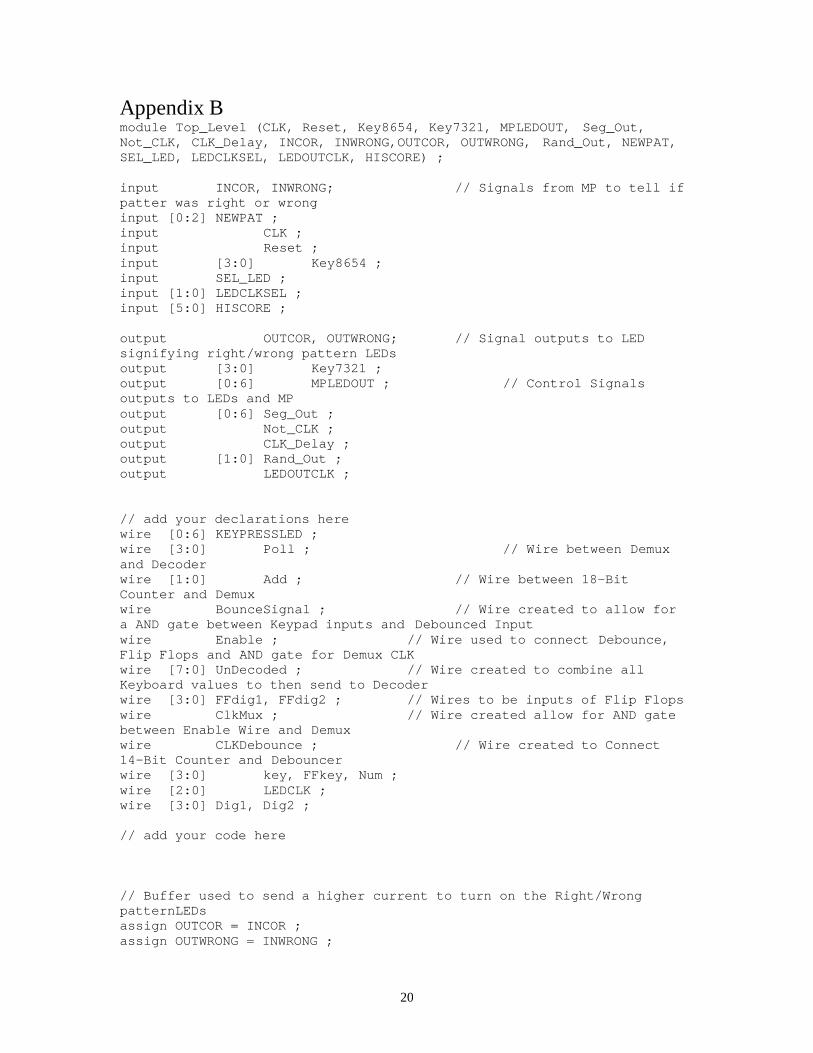
Appendix Bmodule Top_Level (CLK, Reset, Key8654, Key7321, MPLEDOUT, Seg_Out,Not_CLK, CLK_Delay, INCOR, INWRONG,OUTCOR, OUTWRONG, Rand_Out, NEWPAT,SEL_LED, LEDCLKSEL, LEDOUTCLK, HISCORE) ;
input INCOR, INWRONG; // Signals from MP to tell ifpatter was right or wronginput [0:2] NEWPAT ;input CLK ;input Reset ;input [3:0] Key8654 ;input SEL_LED ;input [1:0] LEDCLKSEL ;input [5:0] HISCORE ;
output OUTCOR, OUTWRONG; // Signal outputs to LEDsignifying right/wrong pattern LEDsoutput [3:0] Key7321 ;output [0:6] MPLEDOUT ; // Control Signalsoutputs to LEDs and MPoutput [0:6] Seg_Out ;output Not_CLK ;output CLK_Delay ;output [1:0] Rand_Out ;output LEDOUTCLK ;
// add your declarations herewire [0:6] KEYPRESSLED ;wire [3:0] Poll ; // Wire between Demuxand Decoderwire [1:0] Add ; // Wire between 18-BitCounter and Demuxwire BounceSignal ; // Wire created to allow fora AND gate between Keypad inputs and Debounced Inputwire Enable ; // Wire used to connect Debounce,Flip Flops and AND gate for Demux CLKwire [7:0] UnDecoded ; // Wire created to combine allKeyboard values to then send to Decoderwire [3:0] FFdig1, FFdig2 ; // Wires to be inputs of Flip Flopswire ClkMux ; // Wire created allow for AND gatebetween Enable Wire and Demuxwire CLKDebounce ; // Wire created to Connect14-Bit Counter and Debouncerwire [3:0] key, FFkey, Num ;wire [2:0] LEDCLK ;wire [3:0] Dig1, Dig2 ;
// add your code here
// Buffer used to send a higher current to turn on the Right/WrongpatternLEDsassign OUTCOR = INCOR ;assign OUTWRONG = INWRONG ;

21
// Create AND gate for to pause Demux when keypress foundassign ClkMux = (CLK && ~Enable) ;
// Connect Wire to output for outputing from Demux to Keypadassign Key7321 = Poll ;
// Create AND gate of Keypad inputassign BounceSignal = (Key8654[0] && Key8654[1] && Key8654[2] &&Key8654[3]) ;
// Combine Keypad Signals to one busassign UnDecoded[7] = Key8654[3] ;assign UnDecoded[5] = Key8654[2] ;assign UnDecoded[4] = Key8654[1] ;assign UnDecoded[3] = Key8654[0] ;assign UnDecoded[6] = Poll[3] ;assign UnDecoded[2] = Poll[2] ;assign UnDecoded[1] = Poll[1] ;assign UnDecoded[0] = Poll[0] ;
// Control signal to let MP know a new key was pressedassign MPLEDOUT[0] = Enable ;
assign MPLEDOUT[1:3] = KEYPRESSLED[1:3] ;
// 22 Bit Counter with last two bits outputingCounter_22_Bit Counter_22 (CLK, Reset, Add, LEDCLK, CLKDebounce) ;
// 14 Bit Counter with last bit outputing//Counter_14_Bit Counter_14 (CLK, Reset, CLKDebounce) ;
// DemuxDemux1x4 demux (ClkMux, Add, Poll, Reset) ;
// DebouncerDebounce debouceA (BounceSignal, Enable, CLKDebounce, Reset) ;
// Keyboard DecoderKeyboard_Decoder DecodeKey (UnDecoded, key) ;
//High Score DecoderHSDECODER HighDecoder (HISCORE, Dig1, Dig2) ;
// Flip FlopCFlip_Flop FF3c (key, FFkey, Reset, Enable) ;
// Flip FlopAFlip_Flop FF1a (Dig1, FFdig1, Reset, INWRONG) ;
// Flip FlopBFlip_Flop FF2a (Dig2, FFdig2, Reset, INWRONG) ;
assign Num[3]= FFkey[3] && Enable ;assign Num[2]= FFkey[2] && Enable ;assign Num[1]= FFkey[1] && Enable ;
22
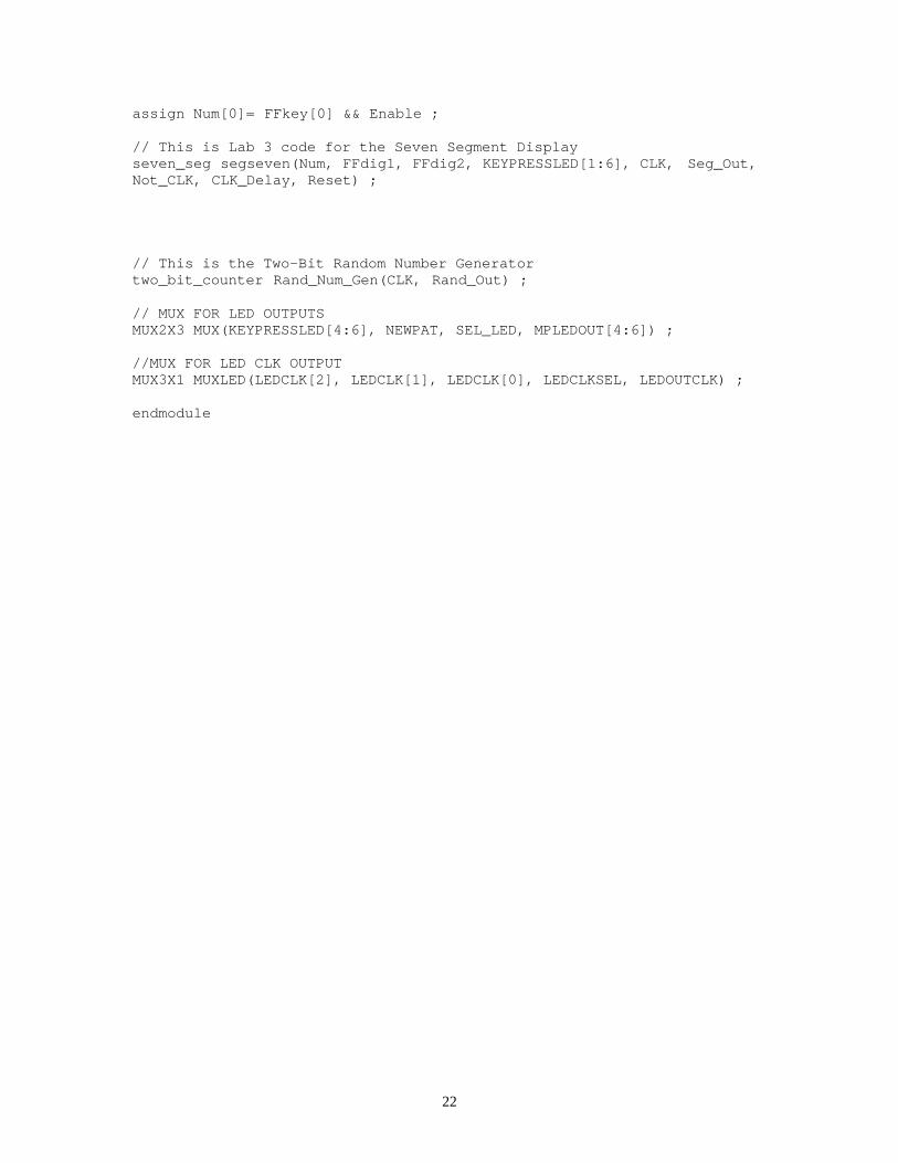
assign Num[0]= FFkey[0] && Enable ;
// This is Lab 3 code for the Seven Segment Displayseven_seg segseven(Num, FFdig1, FFdig2, KEYPRESSLED[1:6], CLK, Seg_Out,Not_CLK, CLK_Delay, Reset) ;
// This is the Two-Bit Random Number Generatortwo_bit_counter Rand_Num_Gen(CLK, Rand_Out) ;
// MUX FOR LED OUTPUTSMUX2X3 MUX(KEYPRESSLED[4:6], NEWPAT, SEL_LED, MPLEDOUT[4:6]) ;
//MUX FOR LED CLK OUTPUTMUX3X1 MUXLED(LEDCLK[2], LEDCLK[1], LEDCLK[0], LEDCLKSEL, LEDOUTCLK) ;
endmodule

23
module seven_seg (SW, FFdig1, FFdig2, MPLEDOUT, CLK, Seg_Out, Not_CLK,CLK_Delay, RESET) ;
input [3:0] SW, FFdig1, FFdig2 ;input CLK ;input RESET ;
output [1:6] MPLEDOUT ; // This is the LED Output andthe info signals to MPreg [1:6] MPLEDOUT ;
output [0:6] Seg_Out ;reg [0:6] Seg_Out ;
output Not_CLK ;output CLK_Delay ;
reg [6:0] state ;
// add all declarations here
// abc_defgparameter BLNK = 7'b111_1111;parameter ZERO = 7'b000_0001;parameter ONE = 7'b100_1111;parameter TWO = 7'b001_0010;parameter THREE = 7'b000_0110;parameter FOUR = 7'b100_1100;parameter FIVE = 7'b010_0100;parameter SIX = 7'b010_0000;parameter SEVEN = 7'b000_1111;parameter EIGHT = 7'b000_0000;parameter NINE = 7'b000_1100;parameter A = 7'b000_1000;parameter B = 7'b110_0000;parameter C = 7'b011_0001;parameter D = 7'b100_0010;parameter E = 7'b011_0000;parameter F = 7'b011_1000;
// wire from Mux to 7-seg decoderwire [3:0] W1 ;
// This is the not of the clock for the one of the two transistorsassign Not_CLK = ~CLK_Delay ;
// This is the Muxassign W1 = CLK_Delay ? FFdig1 : FFdig2;
// add your code here
//Adderalways @(posedge CLK or posedge RESET)
if (RESET) state = 0 ;else state = state + 1;

24
// Output Logicassign CLK_Delay = state[3] ;
// This is the LED Output and the info signals to MPalways @ (SW)
case (SW)1: MPLEDOUT[1:6] <= 6'b000001 ;2: MPLEDOUT[1:6] <= 6'b000010 ;3: MPLEDOUT[1:6] <= 6'b000100 ;4: MPLEDOUT[1:6] <= 6'b011000 ;5: MPLEDOUT[1:6] <= 6'b001000 ;6: MPLEDOUT[1:6] <= 6'b010000 ;default: MPLEDOUT[1:6] <= 6'b000000 ;
endcase
// This is the 7-Seg Displayalways @ (W1)
case (W1)0: Seg_Out <= ZERO;1: Seg_Out <= ONE;2: Seg_Out <= TWO;3: Seg_Out <= THREE;4: Seg_Out <= FOUR;5: Seg_Out <= FIVE;6: Seg_Out <= SIX;7: Seg_Out <= SEVEN;8: Seg_Out <= EIGHT;9: Seg_Out <= NINE;10: Seg_Out <= A;11: Seg_Out <= B;12: Seg_Out <= C;13: Seg_Out <= D;14: Seg_Out <= E;15: Seg_Out <= F;default: Seg_Out <= BLNK;
endcase
endmodule
25
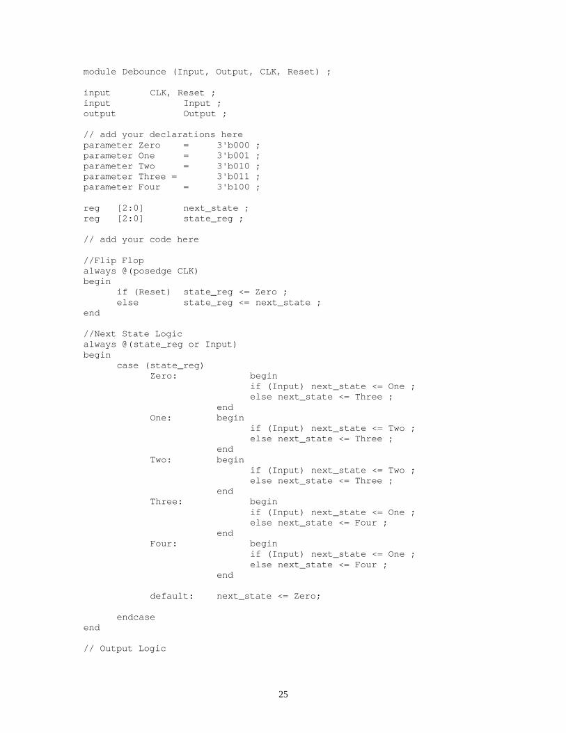
module Debounce (Input, Output, CLK, Reset) ;
input CLK, Reset ;input Input ;output Output ;
// add your declarations hereparameter Zero = 3'b000 ;parameter One = 3'b001 ;parameter Two = 3'b010 ;parameter Three = 3'b011 ;parameter Four = 3'b100 ;
reg [2:0] next_state ;reg [2:0] state_reg ;
// add your code here
//Flip Flopalways @(posedge CLK)begin
if (Reset) state_reg <= Zero ;else state_reg <= next_state ;
end
//Next State Logicalways @(state_reg or Input)begin
case (state_reg)Zero: begin
if (Input) next_state <= One ;else next_state <= Three ;
endOne: begin
if (Input) next_state <= Two ;else next_state <= Three ;
endTwo: begin
if (Input) next_state <= Two ;else next_state <= Three ;
endThree: begin
if (Input) next_state <= One ;else next_state <= Four ;
endFour: begin
if (Input) next_state <= One ;else next_state <= Four ;
end
default: next_state <= Zero;
endcaseend
// Output Logic

26
assign Output = ((state_reg == Four) || (Output && ~(state_reg == Two)&& ~(state_reg == Zero))) ;
endmodule
27
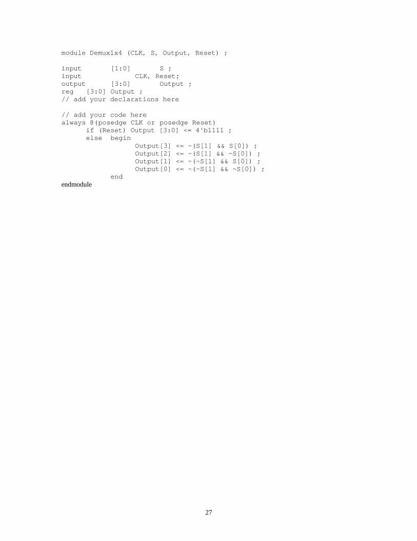
module Demux1x4 (CLK, S, Output, Reset) ;
input [1:0] S ;input CLK, Reset;output [3:0] Output ;reg [3:0] Output ;// add your declarations here
// add your code herealways @(posedge CLK or posedge Reset)
if (Reset) Output [3:0] <= 4'b1111 ;else begin
Output[3] <= ~(S[1] && S[0]) ;Output[2] <= ~(S[1] && ~S[0]) ;Output[1] <= ~(~S[1] && S[0]) ;Output[0] <= ~(~S[1] && ~S[0]) ;
endendmodule
28
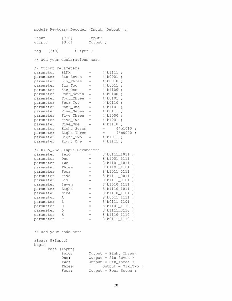
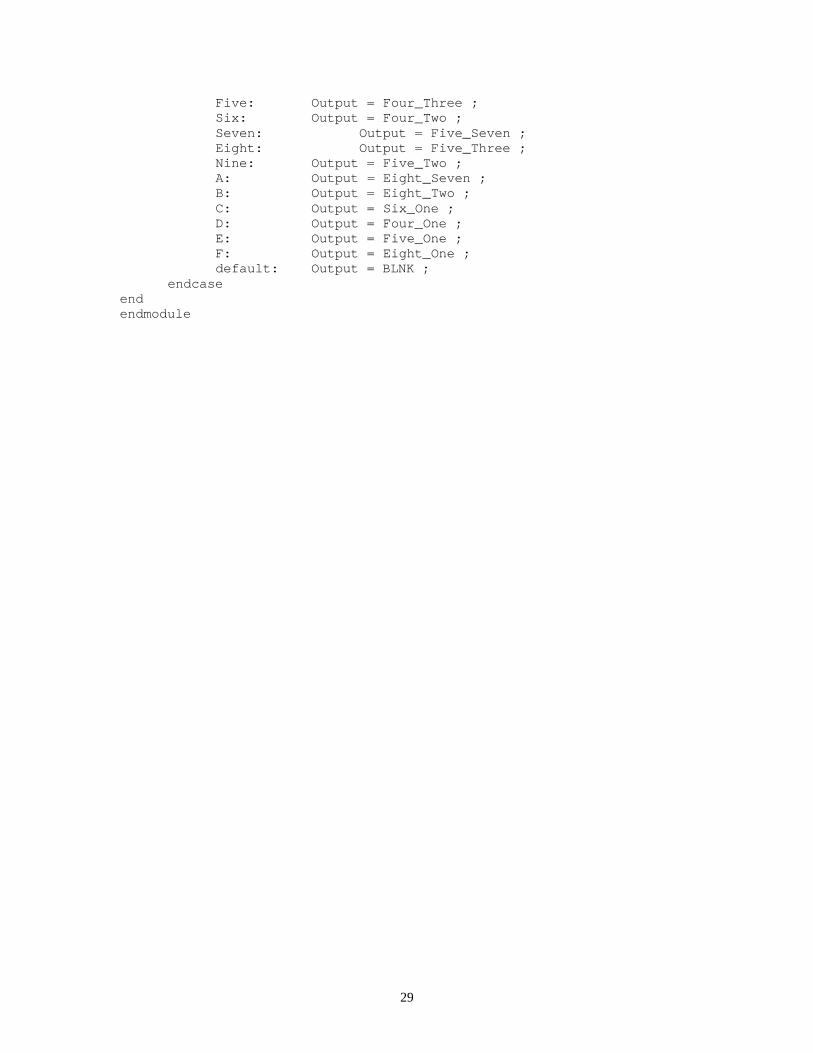
module Keyboard_Decoder (Input, Output) ;
input [7:0] Input;output [3:0] Output ;
reg [3:0] Output ;
// add your declarations here
// Output Parametersparameter BLNK = 4'b1111 ;parameter Six_Seven = 4'b0001 ;parameter Six_Three = 4'b0010 ;parameter Six_Two = 4'b0011 ;parameter Six_One = 4'b1100 ;parameter Four_Seven = 4'b0100 ;parameter Four_Three = 4'b0101 ;parameter Four_Two = 4'b0110 ;parameter Four_One = 4'b1101 ;parameter Five_Seven = 4'b0111 ;parameter Five_Three = 4'b1000 ;parameter Five_Two = 4'b1001 ;parameter Five_One = 4'b1110 ;parameter Eight_Seven = 4'b1010 ;parameter Eight_Three = 4'b0000 ;parameter Eight_Two = 4'b1011 ;parameter Eight_One = 4'b1111 ;
// 8765_4321 Input Parametersparameter Zero = 8'b0111_1011 ;parameter One = 8'b1001_1111 ;parameter Two = 8'b1101_1011 ;parameter Three = 8'b1101_1101 ;parameter Four = 8'b1011_0111 ;parameter Five = 8'b1111_0011 ;parameter Six = 8'b1111_0101 ;parameter Seven = 8'b1010_1111 ;parameter Eight = 8'b1110_1011 ;parameter Nine = 8'b1110_1101 ;parameter A = 8'b0011_1111 ;parameter B = 8'b0111_1101 ;parameter C = 8'b1101_1110 ;parameter D = 8'b1111_0110 ;parameter E = 8'b1110_1110 ;parameter F = 8'b0111_1110 ;
// add your code here
always @(Input)begin
case (Input)Zero: Output = Eight_Three;One: Output = Six_Seven ;Two: Output = Six_Three ;Three: Output = Six_Two ;Four: Output = Four_Seven ;
29
Five: Output = Four_Three ;Six: Output = Four_Two ;Seven: Output = Five_Seven ;Eight: Output = Five_Three ;Nine: Output = Five_Two ;A: Output = Eight_Seven ;B: Output = Eight_Two ;C: Output = Six_One ;D: Output = Four_One ;E: Output = Five_One ;F: Output = Eight_One ;default: Output = BLNK ;
endcaseendendmodule

30
module Flip_Flop (Input, Output, Reset, CLK) ;
input [3:0] Input ;input CLK, Reset ;output [3:0] Output ;reg [3:0] Output ;// add your declarations here
// add your code here
// D Flip Flop with Asynchronous Resetalways @(posedge CLK or posedge Reset)begin if (Reset) //asynchronous RESET active High Output = 4'b0000; else //use CLK rising edge Output = Input;end
endmodule
31
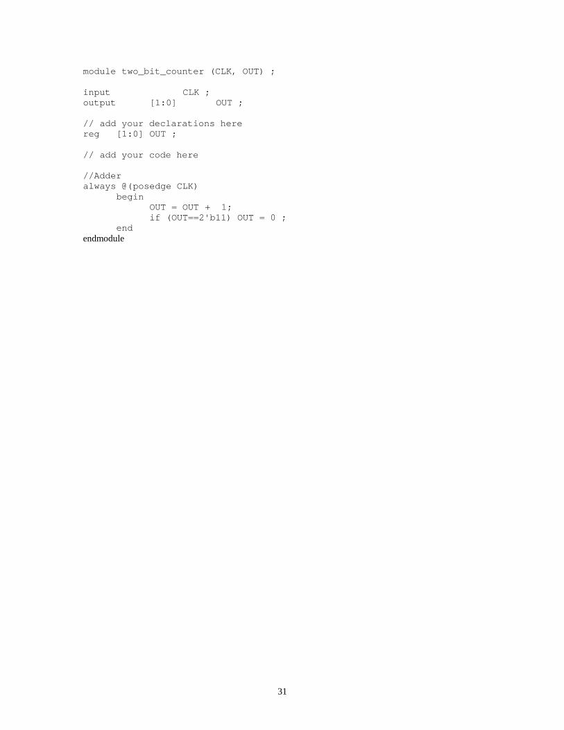
module two_bit_counter (CLK, OUT) ;
input CLK ;output [1:0] OUT ;
// add your declarations herereg [1:0] OUT ;
// add your code here
//Adderalways @(posedge CLK)
beginOUT = OUT + 1;if (OUT==2'b11) OUT = 0 ;
endendmodule

32
module MUX2X3 (IN1, IN2, SEL, OUT) ;
input [0:2] IN1 ;input [0:2] IN2 ;input SEL ;
output [0:2] OUT ;reg [0:2] OUT ;// add your declarations here
// add your code here
always @(SEL or IN1 or IN2)begin case (SEL) 0 : OUT = IN1 ; 1 : OUT = IN2 ;
default : OUT = 0 ; endcaseend
endmodule

33
module Counter_22_Bit (CLK, Reset, Output, CLKOutputs, DebounceOut) ;
input CLK, Reset;output [1:0] Output ;output [2:0] CLKOutputs ;output DebounceOut ;
// add your declarations herereg [21:0] state ;
// add your code here
// Output Logicassign Output[1] = state[16] ;assign Output[0] = state[15] ;assign DebounceOut = state[13] ;
assign CLKOutputs[0] = state[19] ;assign CLKOutputs[1] = state[20] ;assign CLKOutputs[2] = state[21] ;
//Adderalways @(posedge CLK or posedge Reset)begin
if (Reset) state <= 0 ;else state <= state + 1;
end
endmodule

34
module MUX3X1 (IN1, IN2, IN3, SEL, OUT) ;
input IN1 ;input IN2 ;input IN3 ;input [1:0] SEL ;
output OUT ;reg OUT ;// add your declarations here
// add your code here
always @(SEL or IN1 or IN2 or IN3)begin case (SEL) 3 : OUT = IN1 ; 1 : OUT = IN2 ; 2 : OUT = IN3 ;
default : OUT = 0 ; endcaseend
endmodule
35
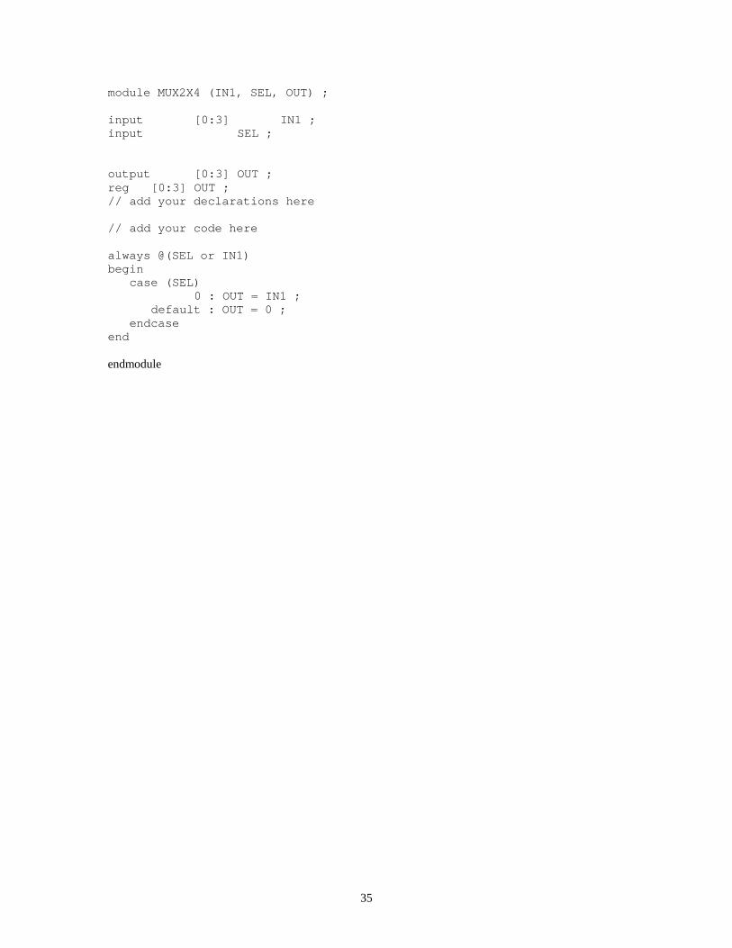
module MUX2X4 (IN1, SEL, OUT) ;
input [0:3] IN1 ;input SEL ;
output [0:3] OUT ;reg [0:3] OUT ;// add your declarations here
// add your code here
always @(SEL or IN1)begin case (SEL) 0 : OUT = IN1 ;
default : OUT = 0 ; endcaseend
endmodule

36
module HSDECODER (Input, Output1, Output2) ;
input [5:0] Input;output [3:0] Output1, Output2 ;
reg [3:0] Output1, Output2 ;
// add your declarations here
// add your code here// This is the decoding for the "ones" digit of the seven segmentdisplayalways @(Input)begin
case (Input)0: Output1 = 4'b0000 ;1: Output1 = 4'b0001 ;2: Output1 = 4'b0010 ;3: Output1 = 4'b0011 ;4: Output1 = 4'b0100 ;5: Output1 = 4'b0101 ;6: Output1 = 4'b0110 ;7: Output1 = 4'b0111 ;8: Output1 = 4'b1000 ;9: Output1 = 4'b1001 ;10: Output1 = 4'b0000 ;11: Output1 = 4'b0001 ;12: Output1 = 4'b0010 ;13: Output1 = 4'b0011 ;14: Output1 = 4'b0100 ;15: Output1 = 4'b0101 ;16: Output1 = 4'b0110 ;17: Output1 = 4'b0111 ;18: Output1 = 4'b1000 ;19: Output1 = 4'b1001 ;20: Output1 = 4'b0000 ;21: Output1 = 4'b0001 ;22: Output1 = 4'b0010 ;23: Output1 = 4'b0011 ;24: Output1 = 4'b0100 ;25: Output1 = 4'b0101 ;26: Output1 = 4'b0110 ;27: Output1 = 4'b0111 ;28: Output1 = 4'b1000 ;29: Output1 = 4'b1001 ;30: Output1 = 4'b0000 ;31: Output1 = 4'b0001 ;32: Output1 = 4'b0010 ;33: Output1 = 4'b0011 ;34: Output1 = 4'b0100 ;35: Output1 = 4'b0101 ;36: Output1 = 4'b0110 ;37: Output1 = 4'b0111 ;38: Output1 = 4'b1000 ;39: Output1 = 4'b1001 ;40: Output1 = 4'b0000 ;

37
41: Output1 = 4'b0001 ;42: Output1 = 4'b0010 ;43: Output1 = 4'b0011 ;44: Output1 = 4'b0100 ;45: Output1 = 4'b0101 ;46: Output1 = 4'b0110 ;47: Output1 = 4'b0111 ;48: Output1 = 4'b1000 ;49: Output1 = 4'b1001 ;50: Output1 = 4'b0000 ;51: Output1 = 4'b0001 ;52: Output1 = 4'b0010 ;53: Output1 = 4'b0011 ;54: Output1 = 4'b0100 ;55: Output1 = 4'b0101 ;56: Output1 = 4'b0110 ;57: Output1 = 4'b0111 ;58: Output1 = 4'b1000 ;59: Output1 = 4'b1001 ;60: Output1 = 4'b0000 ;61: Output1 = 4'b0001 ;62: Output1 = 4'b0010 ;63: Output1 = 4'b0011 ;default: Output1 = 4'b1110 ;
endcaseend// This is the decoding for the "tens" digit of the seven segmentdisplayalways @(Input)begin
case (Input)0: Output2 = 4'b0000 ;1: Output2 = 4'b0000 ;2: Output2 = 4'b0000 ;3: Output2 = 4'b0000 ;4: Output2 = 4'b0000 ;5: Output2 = 4'b0000 ;6: Output2 = 4'b0000 ;7: Output2 = 4'b0000 ;8: Output2 = 4'b0000 ;9: Output2 = 4'b0000 ;10: Output2 = 4'b0001 ;11: Output2 = 4'b0001 ;12: Output2 = 4'b0001 ;13: Output2 = 4'b0001 ;14: Output2 = 4'b0001 ;15: Output2 = 4'b0001 ;16: Output2 = 4'b0001 ;17: Output2 = 4'b0001 ;18: Output2 = 4'b0001 ;19: Output2 = 4'b0001 ;20: Output2 = 4'b0010 ;21: Output2 = 4'b0010 ;22: Output2 = 4'b0010 ;23: Output2 = 4'b0010 ;24: Output2 = 4'b0010 ;25: Output2 = 4'b0010 ;
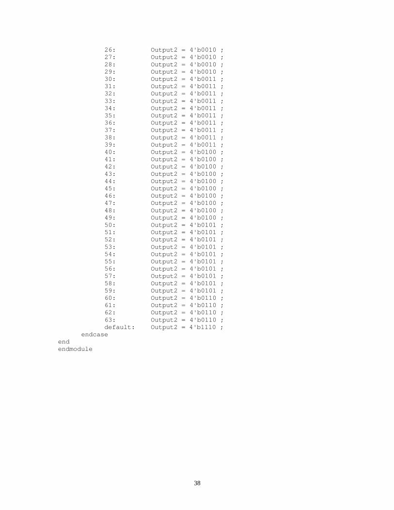
38
26: Output2 = 4'b0010 ;27: Output2 = 4'b0010 ;28: Output2 = 4'b0010 ;29: Output2 = 4'b0010 ;30: Output2 = 4'b0011 ;31: Output2 = 4'b0011 ;32: Output2 = 4'b0011 ;33: Output2 = 4'b0011 ;34: Output2 = 4'b0011 ;35: Output2 = 4'b0011 ;36: Output2 = 4'b0011 ;37: Output2 = 4'b0011 ;38: Output2 = 4'b0011 ;39: Output2 = 4'b0011 ;40: Output2 = 4'b0100 ;41: Output2 = 4'b0100 ;42: Output2 = 4'b0100 ;43: Output2 = 4'b0100 ;44: Output2 = 4'b0100 ;45: Output2 = 4'b0100 ;46: Output2 = 4'b0100 ;47: Output2 = 4'b0100 ;48: Output2 = 4'b0100 ;49: Output2 = 4'b0100 ;50: Output2 = 4'b0101 ;51: Output2 = 4'b0101 ;52: Output2 = 4'b0101 ;53: Output2 = 4'b0101 ;54: Output2 = 4'b0101 ;55: Output2 = 4'b0101 ;56: Output2 = 4'b0101 ;57: Output2 = 4'b0101 ;58: Output2 = 4'b0101 ;59: Output2 = 4'b0101 ;60: Output2 = 4'b0110 ;61: Output2 = 4'b0110 ;62: Output2 = 4'b0110 ;63: Output2 = 4'b0110 ;default: Output2 = 4'b1110 ;
endcaseendendmodule


